Analog Devices AD603SQ-883B, AD603AR-REEL7, AD603AR-REEL, AD603AR, AD603AQ Datasheet
...
Low Noise, 90 MHz
a
FEATURES
“Linear in dB” Gain Control
Pin Programmable Gain Ranges
–11 dB to +31 dB with 90 MHz Bandwidth
9 dB to 51 dB with 9 MHz Bandwidth
Any Intermediate Range, e.g., –1 dB to +41 dB with
30 MHz Bandwidth
Bandwidth Independent of Variable Gain
1.3 nV/√Hz Input Noise Spectral Density
0.5 dB Typical Gain Accuracy
MIL-STD-883 Compliant and DESC Versions Available
APPLICATIONS
RF/IF AGC Amplifier
Video Gain Control
A/D Range Extension
Signal Measurement
PRODUCT DESCRIPTION
The AD603 is a low noise, voltage-controlled amplifier for use
in RF and IF AGC systems. It provides accurate, pin selectable
gains of –11 dB to +31 dB with a bandwidth of 90 MHz or 9 dB
to 51 dB with a bandwidth of 9 MHz. Any intermediate gain
range may be arranged using one external resistor. The input
referred noise spectral density is only 1.3 nV/√Hz and power con-
sumption is 125 mW at the recommended ± 5 V supplies.
The decibel gain is “linear in dB,” accurately calibrated, and
stable over temperature and supply. The gain is controlled at a
high impedance (50 MΩ), low bias (200 nA) differential input;
the scaling is 25 mV/dB, requiring a gain-control voltage of only
Variable-Gain Amplifier
AD603*
1 V to span the central 40 dB of the gain range. An over- and
underrange of 1 dB is provided whatever the selected range. The
gain-control response time is less than 1 µs for a 40 dB change.
The differential gain-control interface allows the use of either
differential or single-ended positive or negative control voltages.
Several of these amplifiers may be cascaded and their gaincontrol gains offset to optimize the system S/N ratio.
The AD603 can drive a load impedance as low as 100 Ω with
low distortion. For a 500 Ω load in shunt with 5 pF, the total
harmonic distortion for a ±1 V sinusoidal output at 10 MHz is
typically –60 dBc. The peak specified output is ±2.5 V minimum into a 500 Ω load, or ±1 V into a 100 Ω load.
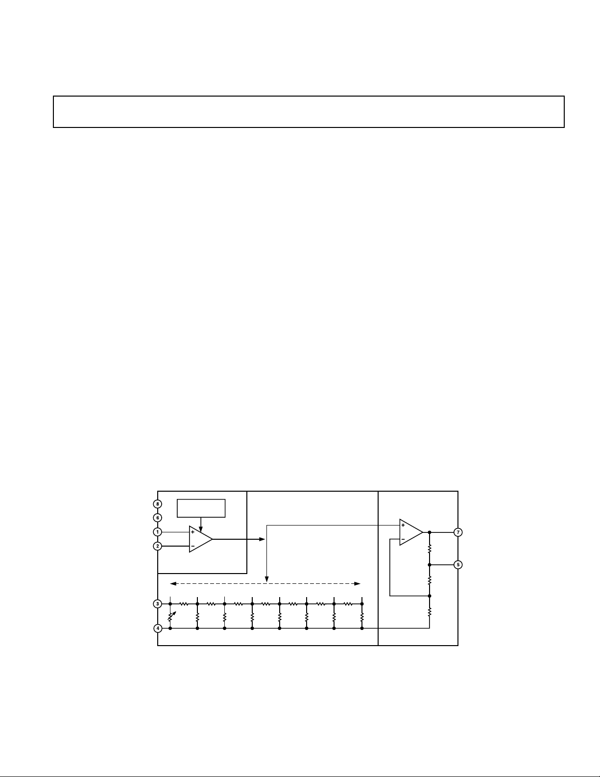
The AD603 uses a proprietary circuit topology—the X-AMP™.
The X-AMP comprises a variable attenuator of 0 dB to –42.14 dB
followed by a fixed-gain amplifier. Because of the attenuator,
the amplifier never has to cope with large inputs and can use
negative feedback to define its (fixed) gain and dynamic performance. The attenuator has an input resistance of 100 Ω, laser
trimmed to ±3%, and comprises a seven-stage R-2R ladder network, resulting in an attenuation between tap points of 6.021 dB.
A proprietary interpolation technique provides a continuous
gain-control function which is linear in dB.
The AD603A is specified for operation from –40°C to +85°C
and is available in both 8-lead SOIC (R) and 8-lead ceramic
DIP (Q). The AD603S is specified for operation from –55°C to
+125°C and is available in an 8-lead ceramic DIP (Q). The
AD603 is also available under DESC SMD 5962-94572.
FUNCTIONAL BLOCK DIAGRAM
VPOS
VNEG
GPOS
GNEG
VINP
COMM
*Patented.
X-AMP is a trademark of Analog Devices, Inc.
SCALING
REFERENCE
V
G
GAIN
CONTROL
INTERFACE
0dB –6.02dB –12.04dB –18.06dB –24.08dB –30.1dB –36.12dB –42.14dB
RRRRR RR
2R 2R 2R 2R 2R 2R R
R = 2R LADDER NETWORK
PRECISION PASSIVE
INPUT ATTENUATOR
REV. D
Information furnished by Analog Devices is believed to be accurate and
reliable. However, no responsibility is assumed by Analog Devices for its
use, nor for any infringements of patents or other rights of third parties
which may result from its use. No license is granted by implication or
otherwise under any patent or patent rights of Analog Devices.
FIXED GAIN
AMPLIFIER
V
OUT
AD603
*NORMAL VALUES
One Technology Way, P.O. Box 9106, Norwood, MA 02062-9106, U.S.A.
Tel: 781/329-4700 World Wide Web Site: http://www.analog.com
Fax: 781/326-8703 © Analog Devices, Inc., 2000
6.44k*
FDBK
694*
20*

(@ TA = 25C, VS = 5 V, –500 mV ≤ VG ≤ +500 mV, GNEG = 0 V, –10 dB to +30 dB Gain
AD603–SPECIFICATIONS
Range, RL = 500 , and CL = 5 pF, unless otherwise noted.)
Model AD603
Parameter Conditions Min Typ Max Unit
INPUT CHARACTERISTICS
Input Resistance Pins 3 to 4 97 100 103 Ω
Input Capacitance 2pF
Input Noise Spectral Density
Noise Figure f = 10 MHz, Gain = max, R
1 dB Compression Point f = 10 MHz, Gain = max, R
1
Input Short Circuited 1.3 nV/√Hz
= 10 Ω 8.8 dB
S
= 10 Ω –11 dBm
S
Peak Input Voltage ±1.4 ±2V
OUTPUT CHARACTERISTICS
–3 dB Bandwidth V
Slew Rate R
Peak Output
2
= 100 mV rms 90 MHz
OUT
≥ 500 Ω 275 V/µs
L
RL ≥ 500 Ω±2.5 ±3.0 V
Output Impedance f ≤ 10 MHz 2 Ω
Output Short-Circuit Current 50 mA
Group Delay Change vs. Gain f = 3 MHz; Full Gain Range ±2ns
Group Delay Change vs. Frequency VG = 0 V; f = 1 MHz to 10 MHz ±2ns
Differential Gain 0.2 %
Differential Phase 0.2 Degree
Total Harmonic Distortion f = 10 MHz, V
= 1 V rms –60 dBc
OUT
3rd Order Intercept f = 40 MHz, Gain = max, RS = 50 Ω 15 dBm
ACCURACY
Gain Accuracy –500 mV ≤ V
T
to T
MIN
Output Offset Voltage
T
MIN
Output Offset Variation vs. V
T
MIN
to T
to T
MAX
MAX
MAX
3
G
VG = 0 V 20 mV
–500 mV ≤ VG ≤ +500 mV 20 mV
≤ +500 mV ±0.5
G
1 dB
±1.5 dB
30 mV
30 mV
GAIN CONTROL INTERFACE
Gain Scaling Factor 39.4 40 40.6 dB/V
to T
T
MIN
GNEG, GPOS Voltage Range
MAX
4
38 42 dB/V
–1.2 +2.0 V
Input Bias Current 200 nA
Input Offset Current 10 nA
Differential Input Resistance Pins 1 to 2 50 MΩ
Response Rate Full 40 dB Gain Change 40 dB/µs
POWER SUPPLY
Specified Operating Range ± 4.75 ±6.3 V
Quiescent Current 12.5 17 mA
T
to T
MIN
NOTES
1
Typical open or short-circuited input; noise is lower when system is set to maximum gain and input is short-circuited. This figure includes the effects of both voltage
and current noise sources.
2
Using resistive loads of 500 Ω or greater, or with the addition of a 1 kΩ pull-down resistor when driving lower loads.
3
The dc gain of the main amplifier in the AD603 is ×35.7; thus, an input offset of 100 µV becomes a 3.57 mV output offset.
4
GNEG and GPOS, gain control, voltage range is guaranteed to be within the range of – VS + 4.2 V to +VS – 3.4 V over the full temperature range of –40°C to +85°C.
Specifications shown in boldface are tested on all production units at final electrical test. Results from those tests are used to calculate outgoing quality levels. All min
and max specifications are guaranteed, although only those shown in boldface are tested on all production units.
Specifications subject to change without notice.
MAX
20 mA
–2–
REV. D

AD603
WARNING!
ESD SENSITIVE DEVICE
ABSOLUTE MAXIMUM RATINGS
1
Supply Voltage ±VS . . . . . . . . . . . . . . . . . . . . . . . . . . . . ± 7.5 V
Internal Voltage VINP (Pin 3) . . . . . . . . . . . ±2 V Continuous
. . . . . . . . . . . . . . . . . . . . . . . . . . . . . . . . . . . . ±V
GPOS, GNEG (Pins 1, 2) . . . . . . . . . . . . . . . . . . . . . . . ± V
for 10 ms
S
S
Internal Power Dissipation2 . . . . . . . . . . . . . . . . . . . . 400 mW
Operating Temperature Range
AD603A . . . . . . . . . . . . . . . . . . . . . . . . . . . – 40°C to +85°C
AD603S . . . . . . . . . . . . . . . . . . . . . . . . . . – 55°C to +125°C
Storage Temperature Range . . . . . . . . . . . . –65°C to +150°C
Lead Temperature Range (Soldering 60 sec) . . . . . . . . . 300°C
NOTES
1
Stresses above those listed under Absolute Maximum Ratings may cause perma-
nent damage to the device. This is a stress rating only; functional operation of the
device at these or any other conditions above those indicated in the operational
section of this specification is not implied. Exposure to absolute maximum rating
conditions for extended periods may affect device reliability.
2
Thermal Characteristics:
8-Lead SOIC Package: θJA = 155°C/W, θJC = 33°C/W
8-Lead Ceramic Package: θJA = 140°C/W, θJC = 15°C/W
ORDERING GUIDE
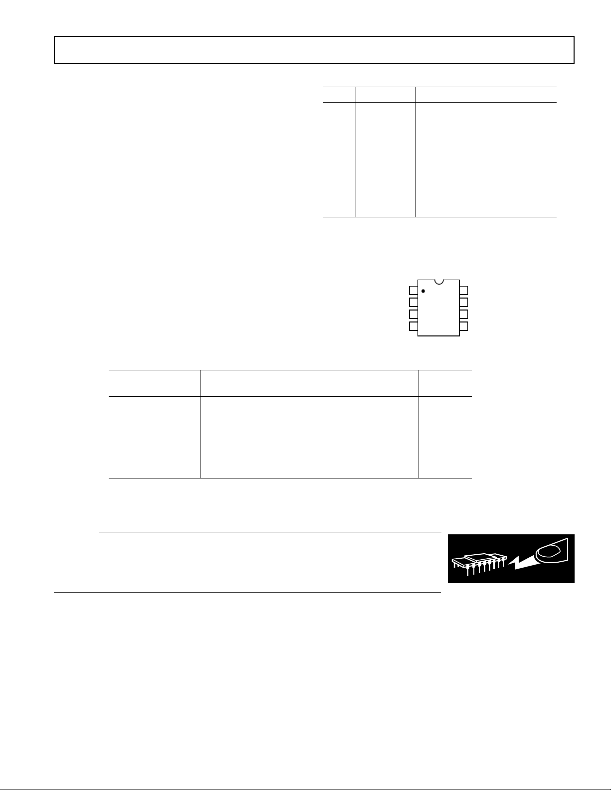
PIN FUNCTION DESCRIPTIONS
Pin Mnemonic Description
1 GPOS Gain-Control Input “HI”
(Positive Voltage Increases Gain)
2 GNEG Gain-Control Input “LO”
(Negative Voltage Increases Gain)
3 VINP Amplifier Input
4 COMM Amplifier Ground
5 FDBK Connection to Feedback Network
6 VNEG Negative Supply Input
7 VOUT Amplifier Output
8 VPOS Positive Supply Input
CONNECTION DIAGRAMS
8-Lead Plastic SOIC (R) Package
8-Lead Ceramic DIP (Q) Package
GPOS
GNEG
VINP
1
2
AD603
TOP VIEW
3
(Not to Scale)
4
8
7
6
5
VPOS
VOUT
VNEG
FDBKCOMM
Temperature Package Package
Part Number Range Description Option
AD603AR –40°C to +85°C 8-Lead SOIC SO-8
AD603AQ –40°C to +85°C 8-Lead Ceramic DIP Q-8
AD603SQ/883B* –55°C to +125°C 8-Lead Ceramic DIP Q-8
AD603-EB Evaluation Board
AD603ACHIPS –40°C to +85°C Die
AD603AR-REEL –40°C to +85°C 13" Reel SO-8
AD603AR-REEL7 –40°C to +85°C 7" Reel SO-8
*Refer to AD603 Military data sheet. Also available as 5962-9457203MPA.
CAUTION
ESD (electrostatic discharge) sensitive device. Electrostatic charges as high as 4000 V readily
accumulate on the human body and test equipment and can discharge without detection. Although
the AD603 features proprietary ESD protection circuitry, permanent damage may occur on devices
subjected to high-energy electrostatic discharges. Therefore, proper ESD precautions are recommended to avoid performance degradation or loss of functionality.
REV. D –3–

AD603
THEORY OF OPERATION
The AD603 comprises a fixed-gain amplifier, preceded by a
broadband passive attenuator of 0 dB to 42.14 dB, having a
gain-control scaling factor of 40 dB per volt. The fixed gain is
laser-trimmed in two ranges, to either 31.07 dB (×35.8) or
50 dB (×358), or may be set to any range in between using one
external resistor between Pins 5 and 7. Somewhat higher gain can
be obtained by connecting the resistor from Pin 5 to common,
but the increase in output offset voltage limits the maximum
gain to about 60 dB. For any given range, the bandwidth is
independent of the voltage-controlled gain. This system provides
an under- and overrange of 1.07 dB in all cases; for example,
the overall gain is –11.07 dB to 31.07 dB in the maximumbandwidth mode (Pin 5 and Pin 7 strapped).
This X-AMP structure has many advantages over former methods
of gain-control based on nonlinear elements. Most importantly,
the fixed-gain amplifier can use negative feedback to increase its
accuracy. Since large inputs are first attenuated, the amplifier
input is always small. For example, to deliver a ±1 V output in
the –1 dB/+41 dB mode (that is, using a fixed amplifier gain of
41.07 dB) its input is only 8.84 mV; thus the distortion can be
very low. Equally important, the small-signal gain and phase
response, and thus the pulse response, are essentially independent of gain.
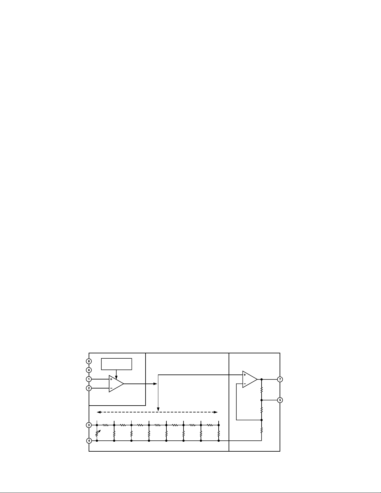
Figure 1 is a simplified schematic. The input attenuator is a
seven-section R-2R ladder network, using untrimmed resistors
of nominally R = 62.5 Ω, which results in a characteristic resistance of 125 Ω ± 20%. A shunt resistor is included at the input
and laser trimmed to establish a more exact input resistance of
100 Ω ± 3%, which ensures accurate operation (gain and HP
corner frequency) when used in conjunction with external resistors
or capacitors.
The nominal maximum signal at input VINP is 1 V rms (±1.4 V
peak) when using the recommended ±5 V supplies, although
operation to ±2 V peak is permissible with some increase in HF
distortion and feedthrough. Pin 4 (SIGNAL COMMON) must
be connected directly to the input ground; significant impedance in
this connection will reduce the gain accuracy.
The signal applied at the input of the ladder network is attenuated by 6.02 dB by each section; thus, the attenuation to each of
the taps is progressively 0 dB, 6.02 dB, 12.04 dB, 18.06 dB,
24.08 dB, 30.1 dB, 36.12 dB and 42.14 dB. A unique circuit
technique is employed to interpolate between these tap-points,
indicated by the “slider” in Figure 1, thus providing continuous
attenuation from 0 dB to 42.14 dB. It will help, in understanding
the AD603, to think in terms of a mechanical means for moving
this slider from left to right; in fact, its “position” is controlled
by the voltage between Pins 1 and 2. The details of the gaincontrol interface are discussed later.
The gain is at all times very exactly determined, and a linear-in-dB
relationship is automatically guaranteed by the exponential
nature of the attenuation in the ladder network (the X-AMP
principle). In practice, the gain deviates slightly from the ideal
law, by about ±0.2 dB peak (see, for example, Figure 16).
Noise Performance
An important advantage of the X-AMP is its superior noise performance. The nominal resistance seen at inner tap points is
41.7 Ω (one third of 125 Ω), which exhibits a Johnson noisespectral density (NSD) of 0.83 nV/√Hz (that is, √4kTR ) at 27°C,
which is a large fraction of the total input noise. The first stage
of the amplifier contributes a further 1 nV/√Hz, for a total input
noise of 1.3 nV/√Hz. It will be apparent that it is essential to use
a low resistance in the ladder network to achieve the very low
specified noise level. The signal’s source impedance forms a
voltage divider with the AD603’s 100 Ω input resistance. In
some applications, the resulting attenuation may be unacceptable, requiring the use of an external buffer or preamplifier to
match a high impedance source to the low impedance AD603.
The noise at maximum gain (that is, at the 0 dB tap) depends
on whether the input is short-circuited or open-circuited: when
shorted, the minimum NSD of slightly over 1 nV/√Hz is achieved;
when open, the resistance of 100 Ω looking into the first tap
generates 1.29 nV/√Hz, so the noise increases to a total of
1.63 nV/√Hz. (This last calculation would be important if the
AD603 were preceded by, for example, a 900 Ω resistor to allow
operation from inputs up to 10 V rms.) As the selected tap
moves away from the input, the dependence of the noise on
source impedance quickly diminishes.
Apart from the small variations just discussed, the signal-tonoise (S/N) ratio at the output is essentially independent of the
attenuator setting. For example, on the –11 dB/+31 dB range
the fixed gain of ×35.8 raises the output NSD to 46.5 nV/√Hz.
Thus, for the maximum undistorted output of 1 V rms and a
1 MHz bandwidth, the output S/N ratio would be 86.6 dB, that
is, 20 log (1 V/46.5 µV).
VPOS
VNEG
GPOS
GNEG
VINP
COMM
SCALING
REFERENCE
V
G
GAIN
CONTROL
INTERFACE
0dB –6.02dB –12.04dB –18.06dB –24.08dB –30.1dB –36.12dB –42.14dB
RRRRR RR
2R 2R 2R 2R 2R 2R R
R = 2R LADDER NETWORK
Figure 1. Simplified Block Diagram of the AD603
*Patented. X-AMP is a trademark of Analog Devices, Inc.
PRECISION PASSIVE
INPUT ATTENUATOR
AD603
–4–
FIXED GAIN
AMPLIFIER
6.44k*
694*
20*
*NORMAL VALUES
V
OUT
FDBK
REV. D

AD603
The Gain-Control Interface
The attenuation is controlled through a differential, highimpedance (50 MΩ) input, with a scaling factor which is
laser-trimmed to 40 dB per volt, that is, 25 mV/dB. An internal
bandgap reference ensures stability of the scaling with respect to
supply and temperature variations.
When the differential input voltage V
= 0 V, the attenuator
G
“slider” is centered, providing an attenuation of 21.07 dB. For
the maximum bandwidth range, this results in an overall gain of
10 dB (= –21.07 dB + 31.07 dB). When the control input is
–500 mV, the gain is lowered by 20 dB (= 0.500 V × 40 dB/V),
to –10 dB; when set to +500 mV, the gain is increased by 20 dB, to
30 dB. When this interface is overdriven in either direction, the
gain approaches either –11.07 dB (= –42.14 dB + 31.07 dB) or
31.07 dB (= 0 + 31.07 dB), respectively. The only constraint on
the gain-control voltage is that it be kept within the common-mode
range (–1.2 V to +2.0 V assuming +5 V supplies) of the gain
control interface.
The basic gain of the AD603 can thus be calculated using the
following simple expression:
Gain (dB) = 40 V
where V
is in volts. When Pins 5 and 7 are strapped (see next
G
+ 10 (1)
G
section) the gain becomes
Gain (dB) = 40 V
+ 20 for 0 to +40 dB
G
and
Gain (dB) = 40 V
+ 30 for +10 to +50 dB (2)
G
The high impedance gain-control input ensures minimal loading
when driving many amplifiers in multiple channel or cascaded
applications. The differential capability provides flexibility in
choosing the appropriate signal levels and polarities for various
control schemes.
For example, if the gain is to be controlled by a DAC providing
a positive only ground-referenced output, the “Gain Control
LO” (GNEG) pin should be biased to a fixed offset of 500 mV, to
set the gain to –10 dB when “Gain Control HI” (GPOS) is at
zero, and to 30 dB when at 1.00 V.
It is a simple matter to include a voltage divider to achieve other
scaling factors. When using an 8-bit DAC having an FS output
of 2.55 V (10 mV/bit), a divider ratio of 2 (generating 5 mV/bit)
would result in a gain-setting resolution of 0.2 dB/bit. The use
of such offsets is valuable when two AD603s are cascaded, when
various options exist for optimizing the S/N profile, as will be
shown later.
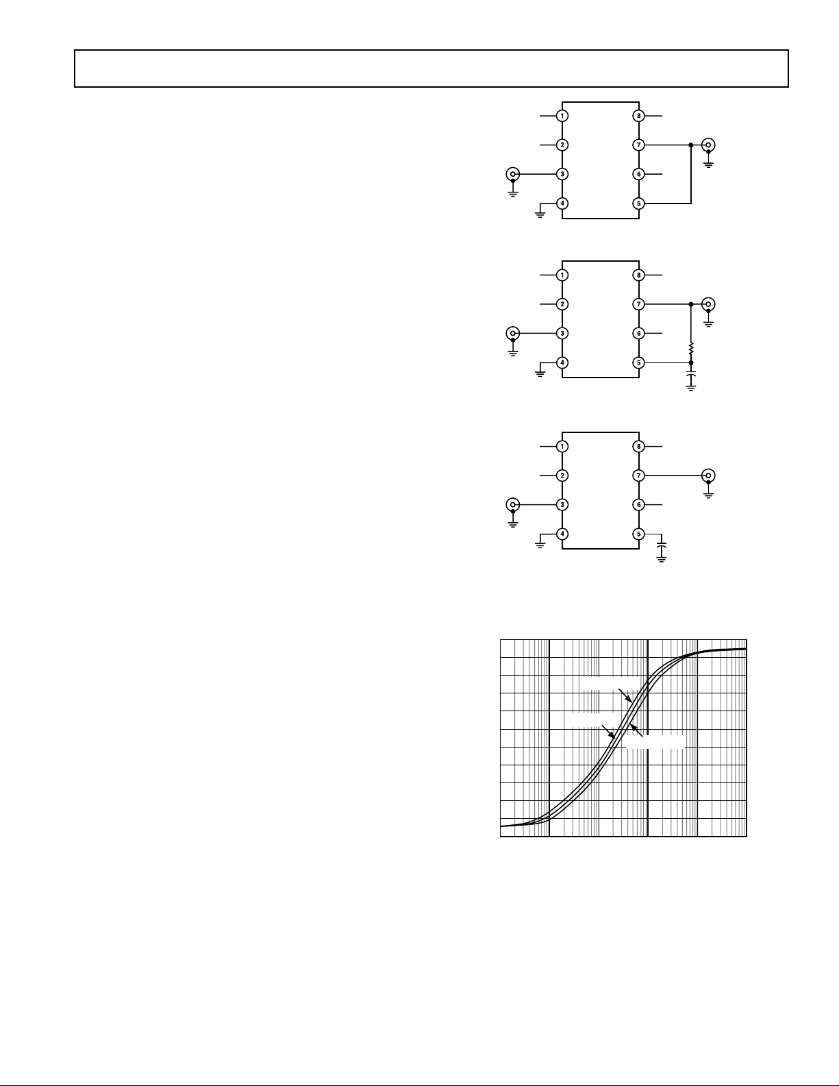
Programming the Fixed-Gain Amplifier Using Pin Strapping
Access to the feedback network is provided at Pin 5 (FDBK).
The user may program the gain of the AD603’s output amplifier
using this pin, as shown in Figure 2. There are three modes: in
the default mode, FDBK is unconnected, providing the range
+9 dB/+51 dB; when V
and FDBK are shorted, the gain is
OUT
lowered to –11 dB/+31 dB; when an external resistor is placed
between V
and FDBK any intermediate gain can be achieved,
OUT
for example, –1 dB/+41 dB. Figure 3 shows the nominal maximum gain versus external resistor for this mode.
VC1
VPOS
VPOS
GPOS
AD603
GNEG
VINP
COMM
V
OUT
VNEG
FDBK
VNEG
V
OUT
VC2
V
IN
a. –10 dB to +30 dB; 90 MHz Bandwidth
VC1
VPOS
VPOS
GPOS
AD603
VC2
V
IN
GNEG
VINP
COMM
V
OUT
VNEG
FDBK
VNEG
2.15k
5.6pF
V
OUT
b. 0 dB to +40 dB; 30 MHz Bandwidth
VC1
VPOS
VPOS
GPOS
AD603
VC2
V
IN
GNEG
VINP
COMM
V
OUT
VNEG
FDBK
VNEG
18pF
V
OUT
c. 10 dB to 50 dB; 9 MHz Bandwidth
Figure 2. Pin Strapping to Set Gain
52
50
48
46
44
42
40
DECIBELS
38
36
34
32
30
10 1M
Figure 3. Gain vs. R
–1:VdB (OUT)
VdB (OUT)
–2:VdB (OUT)
100 1k 10k 100k
EXT
R
EXT
, Showing Worst-Case Limits
Assuming Internal Resistors Have a Maximum Tolerance
of 20%
REV. D –5–
 Loading...