A
查询AD602 供应商查询AD602 供应商
Dual, Low Noise, Wideband
FEATURES
2 channels with independent gain control
Linear in dB gain response
2 gain ranges
AD600: 0 dB to 40 dB
AD602: –10 dB to +30 dB
Accurate absolute gain: ±0.3 dB
Low input noise: 1.4 nV/√Hz
Low distortion: −60 dBc THD at ±1 V output
High bandwidth: dc to 35 MHz (−3 dB)
Stable group delay: ±2 ns
Low power: 125 mW (maximum) per amplifier
Signal gating function for each amplifier
Drives high speed ADCs
MIL-STD-883-compliant and DESC versions available
APPLICATIONS
Ultrasound and sonar time-gain controls
High performance audio and RF AGC systems
Signal measurement
GENERAL DESCRIPTION
The AD600/AD6021 dual channel, low noise, variable gain
amplifiers are optimized for use in ultrasound imaging systems
but are applicable to any application requiring precise gain, low
noise and distortion, and wide bandwidth. Each independent
channel provides a gain of 0 dB to +40 dB in the AD600 and
−10 dB to +30 dB in the AD602. The lower gain of the AD602
results in an improved signal-to-noise ratio (SNR) at the output.
However, both products have the same 1.4 nV/√Hz input noise
spectral density. The decibel gain is directly proportional to the
control voltage, accurately calibrated, and supply and
temperature stable.
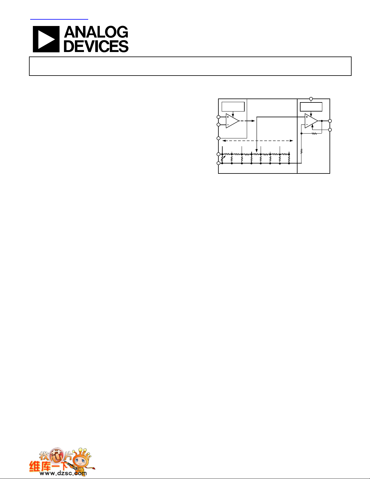
To achieve the difficult performance objectives, a proprietary
circuit form, the X-AMP®, was developed. Each channel of the
X-AMP comprises a variable attenuator of 0 dB to −42.14 dB
followed by a high speed fixed gain amplifier. In this way, the
amplifier never has to cope with large inputs and can benefit
from the use of negative feedback to precisely define the gain
and dynamics. The attenuator is realized as a 7-stage R-2R
ladder network having an input resistance of 100 , laser
trimmed to ±2%. The attenuation between tap points is 6.02 dB;
the gain-control circuit provides continuous interpolation between
these taps. The resulting control function is linear in dB.
Rev. E
Information furnished by Analog Devices is believed to be accurate and reliable. However, no
responsibility is assumed by Anal og Devices for its use, nor for any infringements of patents or ot her
rights of third parties that may result from its use. Specifications subject to change without notice. No
license is granted by implication or otherwise under any patent or patent rights of Analog Devices.
Trademarks and registered trademarks are the property of their respective owners.
Variable Gain Amplifiers
AD600/AD602
FUNCTIONAL BLOCK DIAGRAM
G
T1
–18.06dB
PRECISION PASSIVE
INPUT ATTENUATOR
–22.08dB
–36.12dB
–30.1dB
–42.14dB
Figure 1.
62.5Ω
GATING
INTERFACE
RF2
2.24kΩ (AD600)
694Ω (AD602)
RF1
20Ω
FIXED-GAIN
AMPLIFIER
41.07dB (AD600)
31.07dB (AD602)
SCALING
REFERENCE
C1HI
V
G
C1LO
GAIN CONT ROL
INTERFACE
0dB
–12.04dB
–6.02dB
A1HI
A1LO
500Ω
R-2R LADDER NET WORK
The gain-control interfaces are fully differential, providing an
input resistance of ~15 M and a scale factor of 32 dB/V (that
is, 31.25 mV/dB) defined by an internal voltage reference. The
response time of this interface is less than 1 µs. Each channel
also has an independent gating facility that optionally blocks
signal transmission and sets the dc output level to within a few
millivolts of the output ground. The gating control input is
TTL- and CMOS-compatible.
The maximum gain of the AD600 is 41.07 dB, and the
maximum gain of the AD602 is 31.07 dB; the −3 dB bandwidth
of both models is nominally 35 MHz, essentially independent of
the gain. The SNR for a 1 V rms output and a 1 MHz noise
bandwidth is typically 76 dB for the AD600 and 86 dB for the
AD602. The amplitude response is flat within ±0.5 dB from
100 kHz to 10 MHz; over this frequency range, the group delay
varies by less than ±2 ns at all gain settings.
Each amplifier channel can drive 100 load impedances with
low distortion. For example, the peak specified output is ±2.5 V
minimum into a 500 load or ±1 V into a 100 load. For a
200 load in shunt with 5 pF, the total harmonic distortion for
a ±1 V sinusoidal output at 10 MHz is typically −60 dBc.
The AD600J/AD602J are specified for operation from 0°C to 70°C
and are available in 16-lead PDIP (N) and 16-lead SOIC_W
packages. The AD600A/AD602A are specified for operation from
−40°C to +85°C and are available in 16-lead CERDIP (Q) and
16-lead SOIC_W packages. The AD600S/ AD602S are specified
for operation from −55°C to +125°C, are available in a 16-lead
CERDIP (Q) package, and are MIL-STD-883-compliant. The
AD600S/AD602S are also available under DESC SMD 5962-94572.
1
Patented.
One Technology Way, P.O. Box 9106, Norwood, MA 02062-9106, U.S.A.
Tel: 781.329.4700 www.analog.com
Fax: 781.461.3113 ©2006 Analog Devices, Inc. All rights reserved.
A1OP
A1CM
00538-001

AD600/AD602
TABLE OF CONTENTS
Features .............................................................................................. 1
Applications..................................................................................... 15
Applications....................................................................................... 1
General Description......................................................................... 1
Functional Block Diagram .............................................................. 1
Revision History ............................................................................... 2
Specifications..................................................................................... 3
Absolute Maximum Ratings............................................................ 5
ESD Caution.................................................................................. 5
Pin Configuration and Function Descriptions............................. 6
Typical Performance Characteristics............................................. 7
Theory of Operation ...................................................................... 10
Noise Performance .....................................................................10
The Gain-Control Interface ......................................................11
Signal-Gating Inputs.................................................................. 11
Common-Mode Rejection........................................................ 11
Achieving 80 dB Gain Range.................................................... 12
Time-Gain Control (TGC) and Time-Variable
Gain (TVG)................................................................................. 15
Increasing Output Drive............................................................ 15
Driving Capacitive Loads.......................................................... 15
Realizing Other Gain Ranges ................................................... 16
An Ultralow Noise VCA............................................................ 16
A Low Noise, 6 dB Preamplifier............................................... 16
A Low Noise AGC Amplifier with 80 dB Gain Range.......... 17
A Wide Range, RMS-Linear dB Measurement System (2 MHz
AGC Amplifier with RMS Detector)....................................... 19
100 dB to 120 dB RMS Responding Constant Bandwidth
AGC Systems with High Accuracy dB Outputs..................... 21
A 100 dB RMS/AGC System with Minimal Gain Error
(Parallel Gain with Offset)........................................................ 22
A 120 dB RMS/AGC System with Optimal SNR
(Sequential Gain) ....................................................................... 23
Outline Dimensions .......................................................................27
Sequential Mode (Maximum SNR) .........................................12
Parallel Mode (Simplest Gain-Control Interface).................. 13
Low Ripple Mode (Minimum Gain Error)............................. 13
REVISION HISTORY
1/06—Rev. D to Rev. E
Updated Format..................................................................Universal
Changes to Table 2............................................................................ 5
Changes to The Gain-Control Interface Section........................ 11
Updated Outline Dimensions....................................................... 27
Changes to Ordering Guide.......................................................... 28
3/04—Rev. C to Rev. D
Changes to Specifications................................................................ 2
Changes to Ordering Guide............................................................ 3
Changes to Figure 3.......................................................................... 8
Changes to Figure 29...................................................................... 18
Updated Outline Dimensions....................................................... 20
Ordering Guide .......................................................................... 28
5/02—Rev. B to Rev. C
Changes to Specifications.................................................................2
Renumber Tables and TPCs...................................................Global
8/01—Rev. A to Rev. B
Changes to Accuracy Section of AD600A/AD602A column......2
Rev. E | Page 2 of 28

AD600/AD602
SPECIFICATIONS
Each amplifier section at TA = 25°C, VS = ±5 V, −625 mV ≤ VG ≤ +625 mV, RL = 500 Ω, and CL = 5 pF, unless otherwise noted.
Specifications for the AD600/AD602 are identical, unless otherwise noted.
Table 1.
AD600J/AD602J
Parameter Conditions Min Typ Max Min Typ Max Unit
INPUT CHARACTERISTICS
Input Resistance Pin 2 to Pin 3; Pin 6 to Pin 7
98
100
Input Capacitance 2 2 pF
Input Noise Spectral Density
2
1.4 1.4 nV/√Hz
Noise Figure RS = 50 Ω, maximum gain 5.3 5.3 dB
R
= 200 Ω, maximum gain 2 2 dB
S
Common-Mode Rejection Ratio f = 100 kHz 30 30 dB
OUTPUT CHARACTERISTICS
−3 dB Bandwidth V
= 100 mV rms 35 35 MHz
OUT
Slew Rate 275 275 V/µs
Peak Output
3
RL ≥ 500 Ω ±2.5 ±3 ±2.5 ±3 V
Output Impedance f ≤ 10 MHz 2 2 Ω
Output Short-Circuit Current 50 50 mA
Group Delay Change vs. Gain f = 3 MHz; full gain range ±2 ±2 ns
Group Delay Change vs. Frequency VG = 0 V, f = 1 MHz to 10 MHz ±2 ±2 ns
Total Harmonic Distortion RL= 200 Ω, V
= ±1 V peak, RPD = 1 kΩ −60 −60 dBc
OUT
ACCURACY
AD600
Gain Error 0 dB to 3 dB gain
3 dB to 37 dB gain
37 dB to 40 dB gain
0
−0.5
−1
+0.5
±0.2
−0.5
Maximum Output Offset Voltage4VG = –625 mV to +625 mV 10
Output Offset Variation VG = –625 mV to +625 mV 10
AD602
Gain Error –10 dB to –7 dB gain
–7 dB to +27 dB gain
27 dB to 30 dB gain
0
−0.5
−1
+0.5
±0.2
−0.5
Maximum Output Offset Voltage4VG = −625 mV to +625 mV 5
Output Offset Variation VG = −625 mV to +625 mV 5
GAIN CONTROL INTERFACE
Gain Scaling Factor
+3 dB to +37 dB (AD600);
31.7
32
−7 dB to +27 dB (AD602)
Common-Mode Range −0.75 +2.5 −0.75 +2.5 V
Input Bias Current 0.35 1 0.35 1 A
Input Offset Current 10 50 10 50 nA
Differential Input Resistance Pin 1 to Pin 16; Pin 8 to Pin 9 15 15 MΩ
Response Rate Full 40 dB gain change 40 40 dB/s
Rev. E | Page 3 of 28
1
AD600A/AD602A1
102 95
+1 −0.5
+0.5 −1.0
0 −1.5
50
50
10
10
+1 –0.5
+0.5 −1.0
0 −1.5
30
30
10
10
32.3 30.5
100
+0.5
±0.2
−0.5
+0.5
±0.2
−0.5
32
105
+1.5
+1.0
+0.5
65
65
+1.5
+1.0
+0.5
45
45
33.5
Ω
dB
dB
dB
mV
mV
dB
dB
dB
mV
mV
dB/V

AD600/AD602
AD600J/AD602J
1
AD600A/AD602A1
Parameter Conditions Min Typ Max Min Typ Max Unit
SIGNAL GATING INTERFACE
Logic Input LO (Output On) 0.8 0.8 V
Logic Input HI (Output Off) 2.4 2.4 V
Response Time On to off, off to on 0.3 0.3 µs
Input Resistance Pin 4 to Pin 3; Pin 5 to Pin 6 30 30 kΩ
Output Gated Off
Output Offset Voltage ±10
±100
±10
±400
mV
Output Noise Spectral Density 65 65 nV/√Hz
Signal Feedthrough @ 1 MHz
AD600 −80 −80 dB
AD602 −70 −70 dB
POWER SUPPLY
Specified Operating Range ±4.75 ±5.25 ±4.75 ±5.25 V
Quiescent Current 11
1
Specifications shown in boldface are tested on all production units at final electrical test. Results from those tests are used to calculate outgoing quality levels. All
minimum and maximum specifications guaranteed, although only those shown in boldface are tested on all production units.
2
Typical open- or short-circuited input; noise is lower when the system is set to maximum gain and the input is short-circuited. This figure includes the effects of both
voltage and current noise sources.
3
With an additional 1 kΩ pull-down resistor, if RL < 500 Ω.
4
The dc gain of the main amplifier in the AD600 is × 113; therefore, an input offset of only 100 V becomes an 11.3 mV output offset. In the AD602, the amplifier’s gain
is × 35.7; therefore, an input offset of 100 V becomes a 3.57 mV output offset.
12.5
11
14
mA
Rev. E | Page 4 of 28
AD600/AD602
ABSOLUTE MAXIMUM RATINGS
Table 2.
Parameter Rating
Supply Voltage ±V
Input Voltages
Pin 1, Pin 8, Pin 9, Pin 16 ±V
Pin 2, Pin 3, Pin 6, Pin 7 ±2 V continuous
±VS for 10 ms
Pin 4, Pin 5 ±V
Internal Power Dissipation 600 mW
Operating Temperature Range
J Grade 0°C to 70°C
A Grade −40°C to +85°C
S Grade −55°C to +125°C
Storage Temperature Range −65°C to +150°C
Lead Temperature (Soldering 60 sec) 300°C
θ
JA
16-Lead PDIP 85°C/W
16-Lead SOIC_W 100°C/W
16-Lead CERDIP 120°C/W
S
±7.5 V
S
S
Stresses above those listed under Absolute Maximum Ratings
may cause permanent damage to the device. This is a stress
rating only; functional operation of the device at these or any
other conditions above those indicated in the operational
section of this specification is not implied. Exposure to absolute
maximum rating conditions for extended periods may affect
device reliability.
ESD CAUTION
ESD (electrostatic discharge) sensitive device. Electrostatic charges as high as 4000 V readily accumulate on
the human body and test equipment and can discharge without detection. Although this product features
proprietary ESD protection circuitry, permanent damage may occur on devices subjected to high energy
electrostatic discharges. Therefore, proper ESD precautions are recommended to avoid performance
degradation or loss of functionality.
Rev. E | Page 5 of 28
AD600/AD602
A
A
PIN CONFIGURATION AND FUNCTION DESCRIPTIONS
C1LO
A1HI
1LO
GAT1
GAT2
2LO
A2HI
C2LO
1
2
3
4
5
6
7
8
+
–
–
+
AD600 /
AD602
A1
REF
A2
C1HI
16
A1CM
15
A1OP
14
VPOS
13
VNEG
12
11
A2OP
10
A2CM
9
C2HI
00538-002
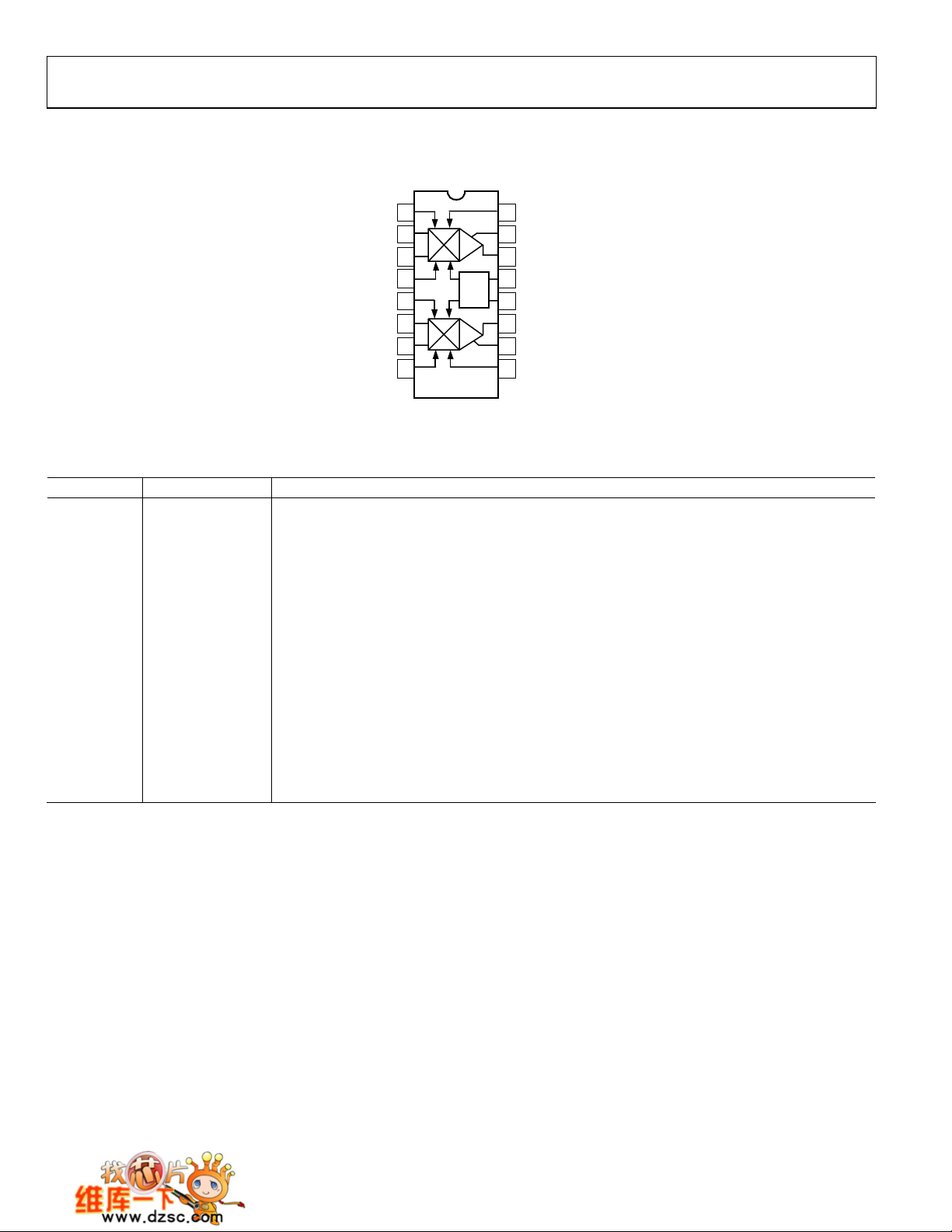
Figure 2. Pin Configuration
Table 3. Pin Function Descriptions
Pin No. Mnemonic Description
1 C1LO CH1 Gain-Control Input LO (Positive Voltage Reduces CH1 Gain)
2 A1HI CH1 Signal Input HI (Positive Voltage Increases CH1 Output)
3 A1LO CH1 Signal Input LO (Usually Connected to CH1 Input Ground)
4 GAT1 CH1 Gating Input (A Logic HI Shuts Off CH1 Signal Path)
5 GAT2 CH2 Gating Input (A Logic HI Shuts Off CH2 Signal Path)
6 A2LO CH2 Signal Input LO (Usually Connected to CH2 Input Ground)
7 A2HI CH2 Signal Input HI (Positive Voltage Increases CH2 Output)
8 C2LO CH2 Gain-Control Input LO (Positive Voltage Reduces CH2 Gain)
9 C2HI CH2 Gain-Control Input HI (Positive Voltage Increases CH2 Gain)
10 A2CM CH2 Common (Usually Connected to CH2 Output Ground)
11 A2OP CH2 Output
12 VNEG Negative Supply for Both Amplifiers
13 VPOS Positive Supply for Both Amplifiers
14 A1OP CH1 Output
15 A1CM CH1 Common (Usually Connected to CH1 Output Ground)
16 C1HI CH1 Gain-Control Input HI (Positive Voltage Increases CH1 Gain)
Rev. E | Page 6 of 28
AD600/AD602
–
TYPICAL PERFORMANCE CHARACTERISTICS
10.0
9.8
9.6
9.4
9.2
9.0
8.8
GROUP DELAY (ns)
8.6
8.4
8.2
8.0
–0.7 0.5
GAIN CONTROL VOLTAGE (V)
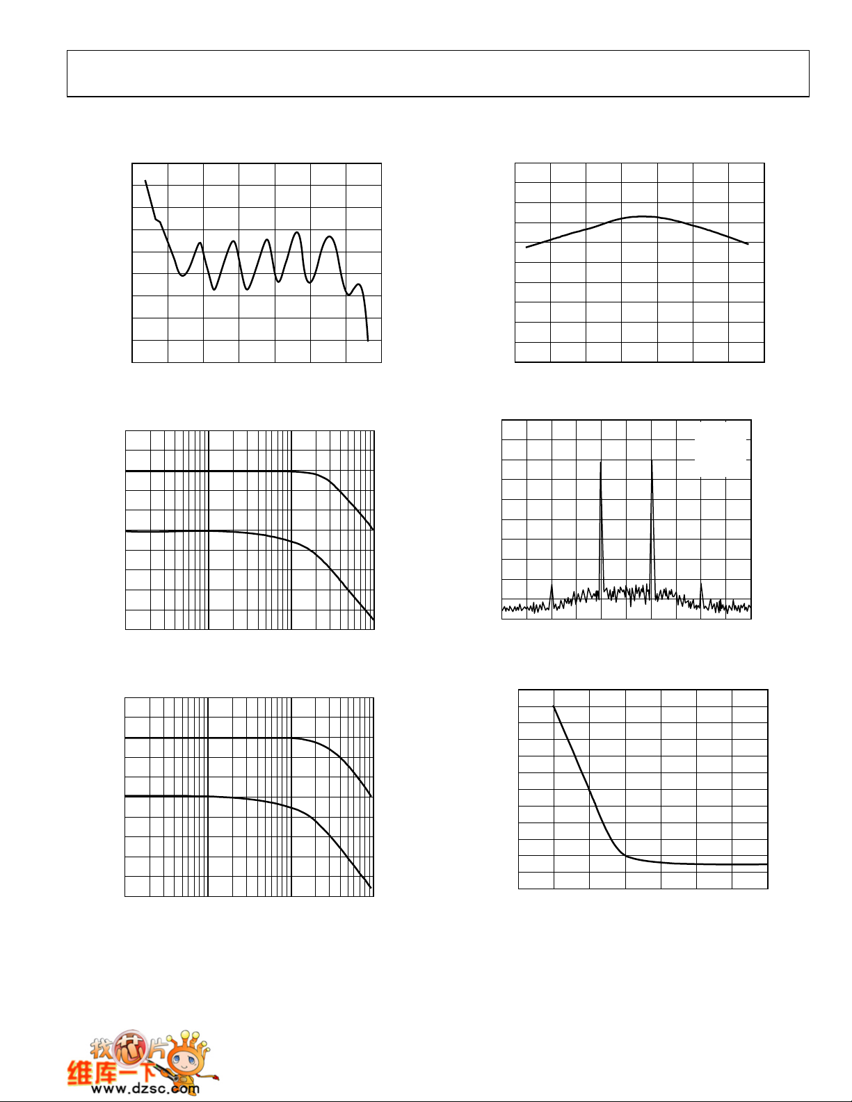
Figure 6. AD600 and AD602 Typical Group Delay vs. V
VG=0V
10dB/DIV
CENTER
FREQ 1MHz
10kHz/DIV
00538-006
0.7–0.5 0.30.1–0.1–0.3
C
–0.05
–0.15
GAIN ERROR (dB)
–0.25
–0.35
–0.45
20dB
17dB
0.45
0.35
0.25
0.15
0.05
–0.5–0.7
GAIN CONTROL VOLTAGE (V)
Figure 3. Gain Error vs. Gain Control Voltage
00538-003
0.7
0.50.30.1–0.1–0.3
0°
–45°
–90°
FREQUENCY (Hz)
Figure 4. AD600 Frequency and Phase Response vs. Gain
10dB
7dB
0°
–45°
–90°
100k 1M 10M 100M
FREQUENCY (Hz)
Figure 5. AD602 Frequency and Phase Response vs. Gain
0538-007
00538-004
100M1M100k 10M
Figure 7. Third-Order Intermodulation Distortion, V
= 2 V p-p, RL = 500 Ω
OUT
1.0
–1.2
–1.4
–1.6
–1.8
–2.0
–2.2
–2.4
–2.6
–2.8
–3.0
NEGATIVE OUTPUT VOLTAGE LIMIT (V)
–3.2
00538-005
–3.4
50
0
LOAD RESISTANCE (Ω)
Figure 8. Typical Output Voltage vs. Load Resistance
20001000500200100
00538-008
(Negative Output Swing Limits First)
Rev. E | Page 7 of 28
AD600/AD602
102
101
100
99
98
97
96
95
INPUT IMPEDANCE (Ω)
94
93
92
100k 1M 10M 100M
GAIN = 40dB
GAIN = 20dB
GAIN = 0dB
FREQUENCY (Hz)
Figure 9. Input Impedance vs. Frequency
6
5
4
3
2
1
0
–1
–2
OUTPUT OFFSETVOLTAGE (mV)
–3
–4
–0.7
–0.3 –0.1 0.1 0.3
–0.5
GAIN CONTROL VO LTAGE (V)
AD600
AD602
0.5
Figure 10. Output Offset Voltage vs. Gain Control Voltage
(Control Channel Feedthrough)
0.7
100
90
OUTPUTINPUT
10
0%
00538-009
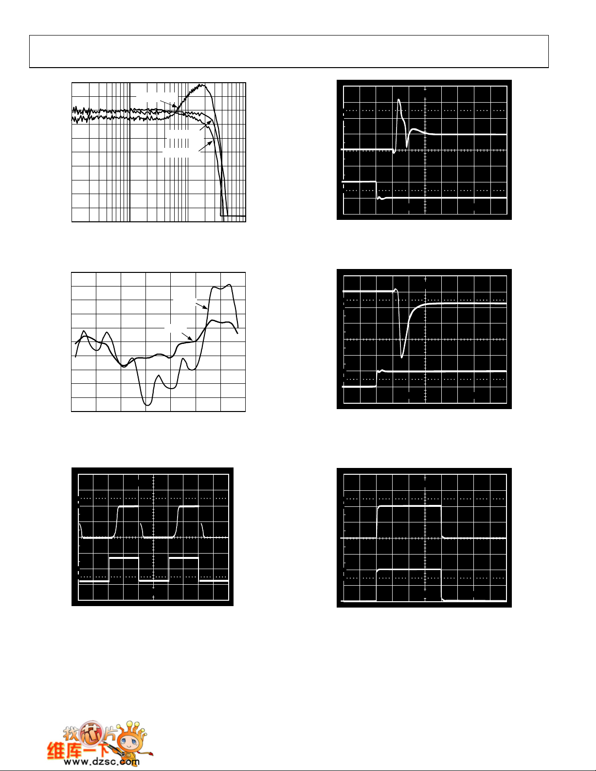
Figure 12. Gating Feedthrough to Output, Gating Off to On
100
90
OUTPUTINPUT
10
0%
00538-010
Figure 13. Gating Feedthrough to Output, Gating On to Off
50mV
5V 100ns
50mV
5V 100ns
00538-012
00538-013
1V VOUT
100
90
OUTPUT
10
INPUT
0%
1V VC
1µs
0538-011
Figure 11. Gain Control Channel Response Time. Top: Output Voltage, 2 V
max, Bottom: Gain Control Voltage V
= ±625 mV
C
Rev. E | Page 8 of 28
1V
100
90
OUTPUTINPUT
10
0%
100mV
500ns
Figure 14. Transient Response, Medium and High Gain
00538-014
AD600/AD602
T
R
T
10
500mV
100
90
OUTPUTINPU
10
0%
1V 200ns
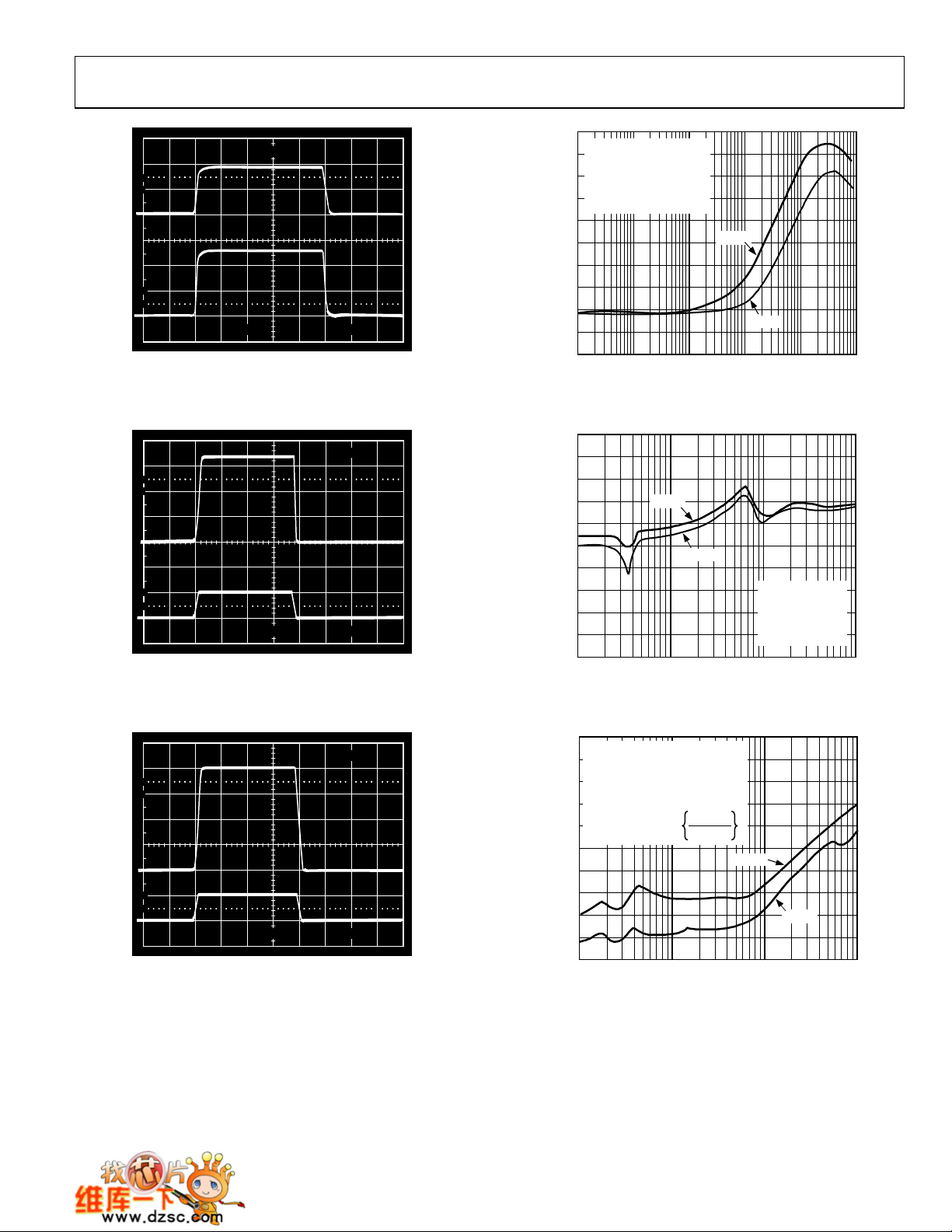
Figure 15. Input Stage Overload Recovery Time
100
90
OUTPUTINPUT
10
0%
200mV 500ns
Figure 16. Output Stage Overload Recovery Time
100
90
OUTPUTINPUT
10
0%
1V 500n s
Figure 17. Transient Response Minimum Gain
1V
500mV
00538-015
00538-016
00538-017
AD600: G = 20dB
5
AD602: G = 10dB
BOTH: V
0
–5
–10
–15
CMRR (dB)
–20
–25
–30
–35
–40
1k 10k 100k 1M 10M 100M
= 100mV rms
CM
V
=±5V
S
R
= 500Ω
L
T
= 25°C
A
AD600
AD602
FREQUENCY (Hz)
Figure 18. CMRR vs. Frequency
20
10
0
–10
–20
–30
PSRR (dB)
–40
–50
–60
–70
–80
100k 1M 10M 100M
AD600
AD602
FREQUENCY (Hz)
AD600: G = 40dB
AD602: G = 30dB
BOTH: R
= 500Ω
L
VIN=0V
R
=50Ω
S
Figure 19. PSRR vs. Frequency
10
AD600: CH1 G = 40dB, VIN = 0
0
–10
–20
–30
ALK (dB)
–40
OSS
–50
C
–60
–70
–80
–90
100k 1M 10M 100M
CH2 G = 20dB, V
AD602: CH1 G = 30dB, V
CH2 G = 0dB, V
BOTH: V
CROSSTALK = 20log
= 1V rms1, RS = 50Ω
OUT
= 500Ω
R
L
= 100mV
IN
= 0
IN
= 316mV
IN
CH1 V
OUT
CH2 V
IN
AD600
FREQUENCY (Hz)
AD602
Figure 20. Crosstalk Between A1 and A2 vs. Frequency
00538-018
00538-019
00538-020
Rev. E | Page 9 of 28
 Loading...