现货库存、技术资料、百科信息、热点资讯,精彩尽在鼎好!
SDA
250 kSPS, 12-Bit Impedance Converter,
FEATURES
Programmable output peak-to-peak excitation voltage
to a max frequency of 100 kHz
Programmable frequency sweep capability with
Frequency resolution of 27 bits (<0.1 Hz)
Impedance measurement range from 100 Ω to 10 MΩ
Phase measurement capability
System accuracy of 0.5%
2.7 V to 5.5 V power supply operation
Temperature range −40°C to +125°C
16-lead SSOP package
APPLICATIONS
Electrochemical analysis
Bioelectrical impedance analysis
Impedance spectroscopy
Complex impedance measurement
Corrosion monitoring and protection equipment
Biomedical and automotive sensors
Proximity sensing
Nondestructive testing
Material property analysis
Fuel/battery cell condition monitoring
serial I
2
C® interface
Network Analyzer
AD5934
GENERAL DESCRIPTION
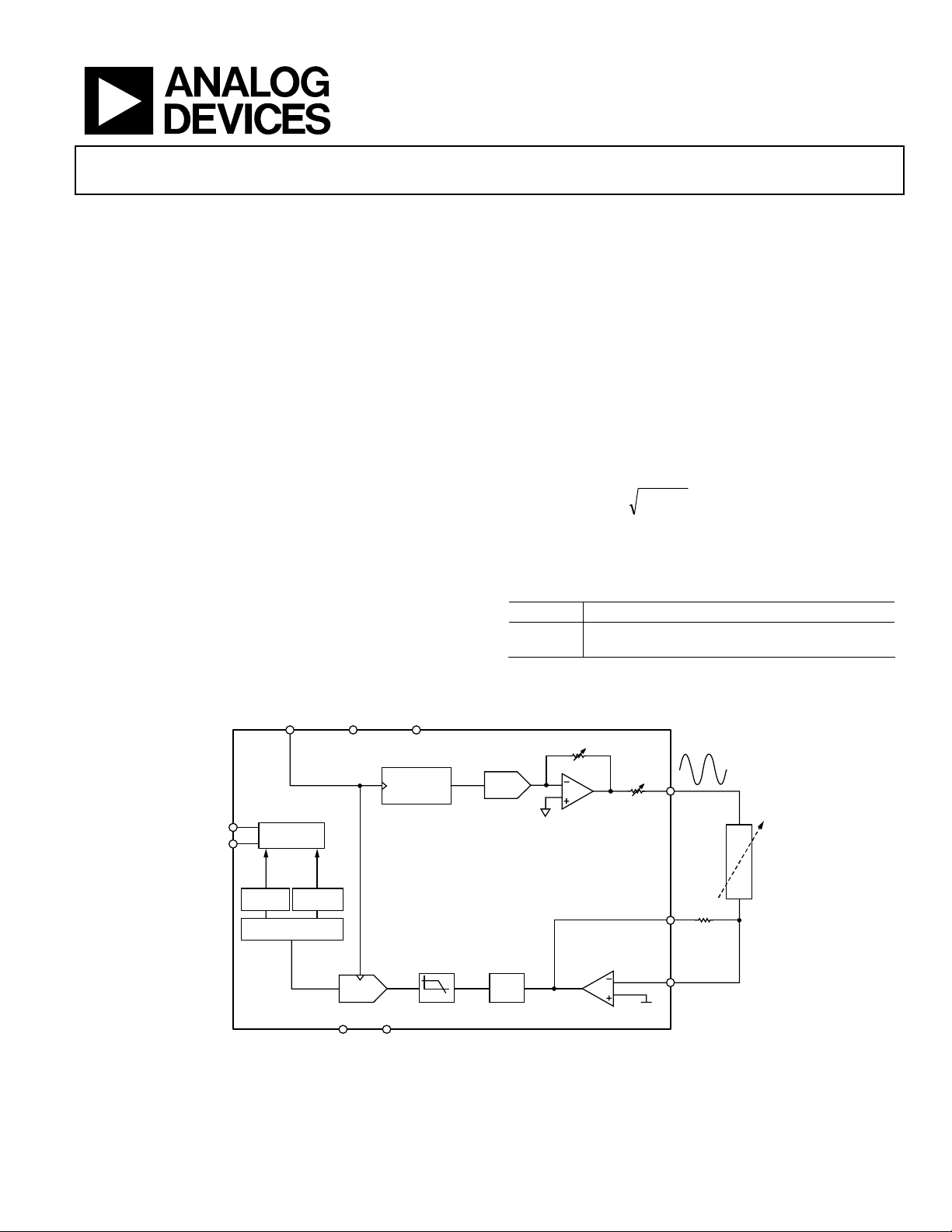
The AD5934 is a high precision impedance converter system
solution which combines an on-board frequency generator with
a 12-bit, 250 kSPS, analog-to-digital converter (ADC). The
frequency generator allows an external complex impedance to
be excited with a known frequency. The response signal from
the impedance is sampled by the on-board ADC and a discrete
Fourier transform (DFT) is processed by an on-board DSP
engine. The DFT algorithm returns a real (R) and imaginary (I)
data-word at each output frequency.
The magnitude of the impedance and relative phase of the
impedance at each frequency point along the sweep is easily
calculated using the following two equations:
22
IRMagnitude +=
)/(1RITanPhase−=
Table 1. Related Devices
Part No. Description
AD5933
2.7 V to 5.5 V. 1 MSPS, 12-bit impedance, with
internal temperature sensor, 16-lead SSOP.
FUNCTIONAL BLOCK DIAGRAM
DVDDAVDDMCLK
DDS
CORE
(27 BITS)
SCL
Rev. 0
Information furnished by Analog Devices is believed to be accurate and reliable.
However, no responsibility is assumed by Analog Devices for its use, nor for any
infringements of patents or other rights of third parties that may result from its use.
Specifications subject to change without notice. No license is granted by implication
or otherwise under any patent or patent rights of Analog Devices. Trademarks and
registered trademarks are the property of their respective owners.
INTERFACE
REAL
REGISTER
1024-POINT DFT
I2C
IMAGINARY
REGISTER
ADC
(12 BITS)
AGND DGND
AD5934
LPF
DAC
GAIN
Figure 1.
R
One Technology Way, P.O. Box 9106, Norwood, MA 02062-9106, U.S.A.
Tel: 781.329.4700 www.analog.com
Fax: 781.461.3113 © 2005 Analog Devices, Inc. All rights reserved.
OUT
VDD/2
VOUT
RFB
VIN
Z(ω)
05325-001

AD5934
TABLE OF CONTENTS
Features .............................................................................................. 1
Applications....................................................................................... 1
General Description ......................................................................... 1
Functional Block Diagram .............................................................. 1
Specifications..................................................................................... 3
2
I
C Serial Interface Timing Characteristics .................................. 5
Absolute Maximum Ratings............................................................ 6
ESD Caution.................................................................................. 6
Pin Configuration and Descriptions.............................................. 7
Typical Performance Characteristics ............................................. 8
Te r mi n ol o g y .................................................................................... 10
System Description......................................................................... 11
Transmit Stage............................................................................. 12
Frequency Sweep Command Sequence................................... 13
Receive Stage ............................................................................... 13
DFT Operation ........................................................................... 13
Impedance Calculation .................................................................. 14
Magnitude Calculation.............................................................. 14
Gain Factor Calculation ............................................................ 14
Impedance Calculation Using Gain Factor............................. 14
Gain Factor Variation with Frequency .................................... 14
Two-Point Calibration............................................................... 15
Two-Point Gain Factor Calculation......................................... 15
Gain Factor Setup Configuration............................................. 15
Gain Factor Recalculation......................................................... 15
Gain Factor Temperature Variation......................................... 16
Impedance Error ........................................................................ 16
Performing a Frequency Sweep .................................................... 18
Register Map ................................................................................... 19
Control Register ......................................................................... 19
Start Frequency Register ........................................................... 20
Frequency Increment Register.................................................. 20
Number of Increments Register ............................................... 21
Number of Settling Time Cycles Register............................... 21
Status Register............................................................................. 22
Real and Imaginary Data Registers (16 Bits).......................... 22
Serial Bus Interface......................................................................... 23
General I
Writing/Reading to the AD5934 .............................................. 24
Block Write.................................................................................. 24
AD5934 Read Operations ......................................................... 25
Typical Applications ....................................................................... 26
Biomedical: Noninvasive Blood impedance Measurement .. 26
Sensor/Complex Impedance Measurement............................ 26
Electro-Impedance Spectroscopy............................................. 27
Choosing a Reference for the AD5934........................................ 28
Layout and Configuration............................................................. 29
Power Supply Bypassing and Grounding................................ 29
Outline Dimensions....................................................................... 30
Ordering Guide .......................................................................... 30
2
C Timing.................................................................... 23
REVISION HISTORY
6/05—Revision 0: Initial Version
Rev. 0 | Page 2 of 32

AD5934
SPECIFICATIONS
Test conditions unless otherwise stated: VDD = 3.3 V, MCLK = 16.776 MHz, 2 V p-p output excitation voltage @ 30 kHz, 200 kΩ
connected between Pin 5 and Pin 6. Feedback resistor = 200 kΩ connected between Pin 4 and Pin 5. PGA gain = ×1.
Table 2.
Y Version
Parameter Min Typ Max Unit Test Conditions/Comments
SYSTEM
Impedance Range 0.001 10 MΩ
Total System Accuracy 0.5 %
System Impedance Error Drift 30 ppm/°C
TRANSMIT STAGE
Output Frequency Range
2
1
100 kHz
Output Frequency Resolution 0.1 Hz
MCLK Frequency 16.776 MHz Maximum system clock frequency.
TRANSMIT OUTPUT VOLTAGE
Range 1
AC Output Excitation Voltage
4
DC Bias
3
1.98 V p-p
1.48 V
DC Output Impedance 200 Ω TA = 25°C.
Short-Circuit Current to Ground
±5.8 mA T
at VOUT
Range 2
AC Output Excitation Voltage
4
DC Bias
3
0.97 V p-p See Figure 6.
0.76 V
DC Output Impedance 2.4 kΩ
Short-Circuit Current to Ground
±0.25 mA
at VOUT
Range 3
AC Output Excitation Voltage
4
DC Bias
3
0.383 V p-p See Figure 8.
0.31 V
DC Output Impedance 1 kΩ
Short-Circuit Current to Ground
±0.20 mA
at VOUT
Range 4
AC Output Excitation Voltage
4
DC Bias
3
0.198 V p-p See Figure 10.
0.173 V
DC Output Impedance 600 Ω
Short-Circuit Current to Ground
±0.15 mA
at VOUT
Short-Circuit Current to Ground ±0.15 mA
SYSTEM AC CHARACTERISTICS
Signal-to-Noise Ratio 60 dB
Total Harmonic Distortion −52 dB
Spurious-Free Dynamic Range
Wide Band (0 MHz to 1 MHz) −56 dB
Narrowband (±5 kHz) −85 dB
1
<0.1 Hz resolution achievable using
DDS techniques.
Refer to
Figure 4 for output voltage
distribution.
DC bias of the AC excitation signal.
Figure 5.
See
= 25°C.
A
DC bias of output excitation signal.
Figure 7.
See
DC bias of output excitation signal.
See
Figure 9.
DC bias of output excitation signal.
Figure 11.
See
Rev. 0 | Page 3 of 32

AD5934
Y Version
1
Parameter Min Typ Max Unit Test Conditions/Comments
RECEIVE STAGE
Input Leakage Current 1 nA To VIN pin.
Input Capacitance
5
0.01 fF
Pin capacitance between VOUT and
GND.
Feedback Capacitance C
FB
3 pF
Feedback capacitance around currentto-voltage amplifier; appears in parallel
with feedback resistor.
ANALOG-TO-DIGITAL CONVERTER
Resolution
Sampling Rate
5
12 bits
250 kSPS ADC throughput rate.
LOGIC INPUTS
Input High Voltage (VIH) 0.7 × VDD
Input Low Voltage (VIL) 0.3 × VDD
Input Current
6
1 μA TA =25°C.
Input Capacitance 7 pF TA = 25°C.
POWER REQUIREMENTS
VDD 2.7 5.5 V
IDD (Normal Mode ) 10 15 mA VDD = 3.3 V.
17 25 mA VDD = 5.5 V.
IDD (Standby Mode) 7 mA
VDD = 3.3 V; see the
Control Register
section.
9 mA VDD = 5.5 V.
IDD (Power-Down Mode) 0.7 5 μA VDD = 3.3 V.
1 8 μA VDD = 5.5 V.
1
Temperature range for Y version = −40°C to +125°C, typical at 25°C.
2
The lower limit of the output excitation frequency can be lowered by scaling the clock supplied to the AD5934.
3
The peak-to-peak value of the AC output excitation voltage scales with supply voltage according to the formula given below. VDD is the supply voltage.
4
The DC bias value of the Output excitation voltage scales with supply voltage according to the formula given below. VDD is the supply voltage.
5
Guaranteed by design or characterization, not production tested. Input capacitance at the VOUT pin is equal to pin capacitance divided by open-loop gain of current-
to-voltage amplifier.
6
The accumulation of the currents into Pin 8, Pin 15, and Pin 16.
2
3.3
3.3
VDDVoltageitationOutput Exc ×=
2
VDDVoltage Biasn ExcitatioOutput ×=
p)-p(V
(V)
Rev. 0 | Page 4 of 32
AD5934
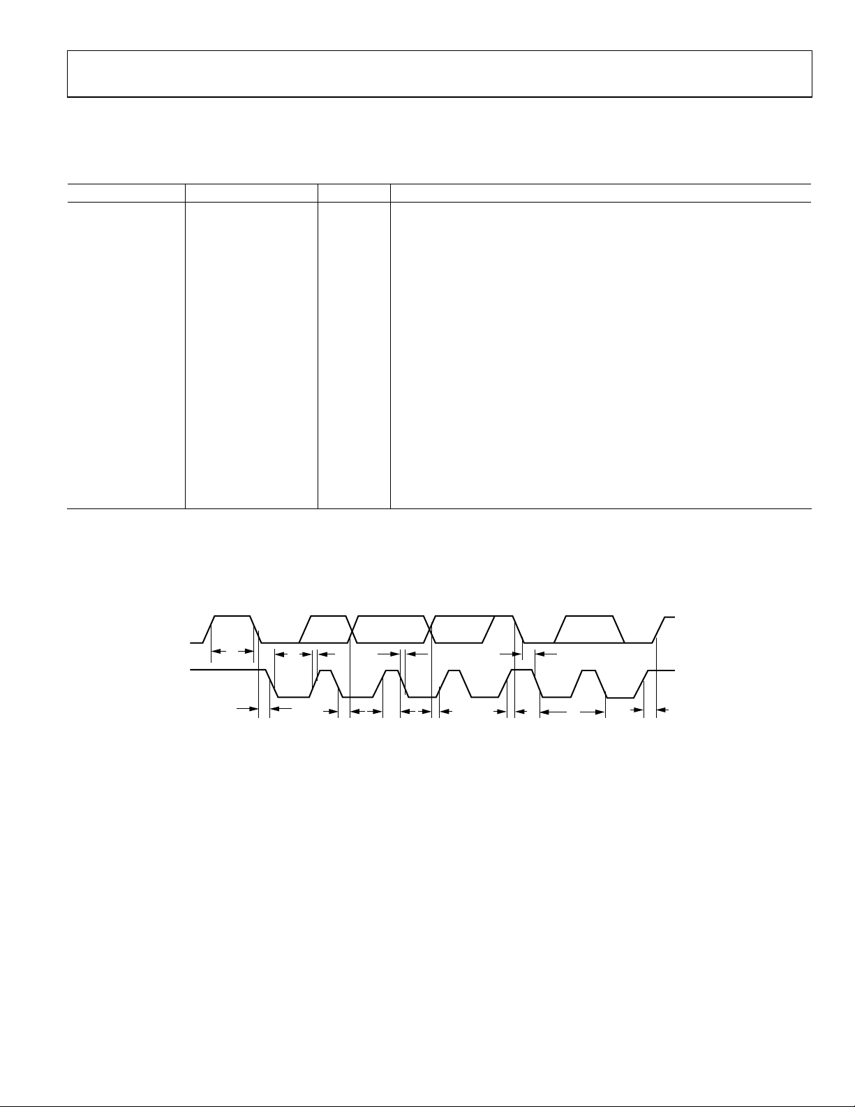
I2C SERIAL INTERFACE TIMING CHARACTERISTICS
VDD = 2.7 V to 5.5 V. All specifications T
Table 3.
Parameter
F
SCL
t
1
t
2
t
3
t
4
t
5
3
t
6
2
Limit at T
MIN
, T
MAX
400 kHz max SCL clock frequency
2. 5 μs min SCL cycle time
0. 6 μs min t
1. 3 μs min t
0. 6 μs min tHD,
100 ns min tSU,
0. 9 μs max tHD,
0 μs min tHD,
t
7
t
8
t
9
t
10
0. 6 μs min tSU,
0. 6 μs min tSU,
1. 3 μs min t
300 ns max tF, rise time of SDA when transmitting
0 ns min tR, rise time of SCL and SDA when receiving (CMOS compatible)
t
11
300 ns max tF, fall time of SCL and SDA when transmitting
0 ns min tF, fall time of SDA when receiving (CMOS compatible)
250 ns max tF, fall time of SDA when receiving
20 + 0.1 C
C
B
1
See Figure 2.
2
Guaranteed by design and characterization, not production tested.
3
A master device must provide a hold time of at least 300 ns for the SDA signal (referred to V
4
CB is the total capacitance of one bus line in pF. Note that tR and tF are measured between 0.3 VDD and 0.7 VDD.
400 pF max Capacitive load for each bus line
4
B
MIN
to T
, unless otherwise noted.
MAX
Unit Description
, SCL high time
HIGH
, SCL low time
LOW
, start/repeated start condition hold time
STA
, data setup time
DAT
, data hold time
DAT
, data hold time
DAT
, setup time for repeated start
STA
, stop condition setup time
STO
, bus free time between a stop and a start condition
BUF
ns min tF, fall time of SCL and SDA when transmitting
1
of the SCL signal) in order to bridge the undefined SCL’s falling edge.
IH MIN
SDA
t
SCL
9
START
CONDITION
t
3
t
4
t
10
t
6
t
11
Figure 2. I
t
2
2
C Interface Timing Diagram
t
t
5
7
REPEATED
START
CONDITION
t
4
t
1
t
8
STOP
CONDITION
05325-002
Rev. 0 | Page 5 of 32
AD5934
ABSOLUTE MAXIMUM RATINGS
TA = 25°C, unless otherwise note
Table 4.
Parameter Rating
DVDD to GND −0.3 V to + 7. 0 V
AVDD1 to GND −0.3 V to + 7. 0 V
AVDD2 to GND −0.3 V to + 7. 0 V
SDA/SCL to GND −0.3 V to VDD + 0.3 V
VOUT to GND −0.3 V to VDD + 0.3 V
VIN to GND −0.3 V to VDD + 0.3 V
MCLK to GND −0.3 V to VDD + 0.3 V
Operating Temperature Range
Extended Industrial (Y Grade) −40°C to +125°C
Storage Temperature Range −65°C to +160°C
Maximum Junction Temperature 150°C
SSOP Package
θJA Thermal Impedance 139°C/W
θJC Thermal Impedance 136°C/W
Reflow Soldering (Pb-Free)
Peak Temperature 260°C
Time at Peak Temperature 10 sec to 40 sec
Stresses above those listed under Absolute Maximum Ratings
may cause permanent damage to the device. This is a stress
rating only; functional operation of the device at these or any
other conditions above those listed in the operational sections
of this specification is not implied. Exposure to absolute
maximum rating conditions for extended periods may affect
device reliability.
ESD CAUTION
ESD (electrostatic discharge) sensitive device. Electrostatic charges as high as 4000 V readily accumulate on
the human body and test equipment and can discharge without detection. Although this product features
proprietary ESD protection circuitry, permanent damage may occur on devices subjected to high energy
electrostatic discharges. Therefore, proper ESD precautions are recommended to avoid performance
degradation or loss of functionality.
Rev. 0 | Page 6 of 32

AD5934
K
PIN CONFIGURATION AND DESCRIPTIONS
NC
1
NC
2
3
NC
RFB
VIN
VOUT
NC
MCL
AD5934
4
TOP VIEW
(Not to Scale)
5
6
7
8
NC = NO CONNECT
Figure 3. Pin Configuration
It is recommended to tie all supply connections (Pin 9, Pin 10, and Pin 11) and run from a single supply between 2.7 V and 5.5 V. It is also
recommended to connect all ground signals together (Pin 12, Pin 13, and Pin 14).
Table 5. Pin Function Descriptions
Pin No. Mnemonic Description/comment
1, 2, 3, 7 NC No Connect.
4 RFB
External Feedback Resistor. Connected from Pin 4 to Pin 5 and used to set the gain of the current-to-voltage
amplifier on the receive side.
5 VIN Input to Receive Transimpedance Amplifier. Presents a virtual earth voltage of VDD/2.
6 VOUT Excitation Voltage Signal Output.
8 MCLK Master Clock for the System. Supplied by user.
9 DVDD Digital Supply Voltage.
10 AVDD1 Analog Supply Voltage 1.
11 AVDD2 Analog Supply Voltage 2.
12 DGND Digital Ground.
13 AGND1 Analog Ground 1.
14 AGND2 Analog Ground 2.
15 SDA I2C Data Input.
16 SCL I2C Clock Input.
16
15
14
13
12
11
10
9
SCL
SDA
AGND2
AGND1
DGND
AVDD2
AVDD1
DVDD
05325-003
Rev. 0 | Page 7 of 32
AD5934
TYPICAL PERFORMANCE CHARACTERISTICS
35
MEAN = 1.9824
SIGMA = 0.0072
30
30
MEAN = 0.7543
SIGMA = 0.0099
25
25
20
15
NUMBER OF DEVICES
10
5
0
1.92 1.94 1.96 1.98 2.00 2.02 2.04
VOLTAGE (V)
2.06
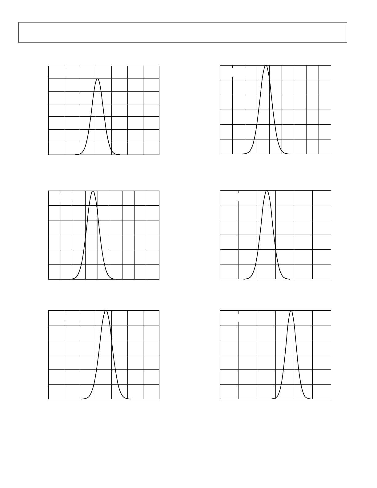
Figure 4. Range 1: Output Excitation Voltage Distribution VDD = 3.3 V
30
MEAN = 1.4807
SIGMA = 0.0252
25
20
15
10
NUMBER OF DEVICES
5
05325-064
20
15
10
NUMBER OF DEVICES
5
0
0.68
0.70 0.72 0.74 0.76 0.78 0.80 0.82 0.84
VOLTAGE (V)
Figure 7. Range 2: DC Bias Distribution VDD = 3.3 V
30
MEAN = 0.3827
SIGMA = 0.00167
25
20
15
10
NUMBER OF DEVICES
5
0.86
05325-073
0
1.30
1.35 1.40 1.45 1.50 1.55 1.60 1.65 1.70
VOLTAGE (V)
1.75
Figure 5. Range 1: DC Bias Distribution VDD = 3.3 V
30
MEAN = 0.9862
SIGMA = 0.0041
25
20
15
10
NUMBER OF DEVICES
5
0
0.95 0.96 0.97 0.98 0.99 1.00 1.01 1.02
VOLTAGE (V)
Figure 6. Range 2: Output Excitation Voltage Distribution VDD = 3.3 V
05325-072
05325-066
0
0.370
0.375 0.380 0.385 0.390 0.395
VOLTAGE (V)
0.400
Figure 8. Range 3: Output Excitation Voltage Distribution VDD = 3.3 V
30
MEAN = 0.3092
SIGMA = 0.0014
25
20
15
10
NUMBER OF DEVICES
5
0
0.290
0.295 0.300 0.305 0.310 0.315
VOLTAGE (V)
0.320
Figure 9. Range 3: DC Bias Distribution VDD = 3.3 V
05325-077
05325-074
Rev. 0 | Page 8 of 32
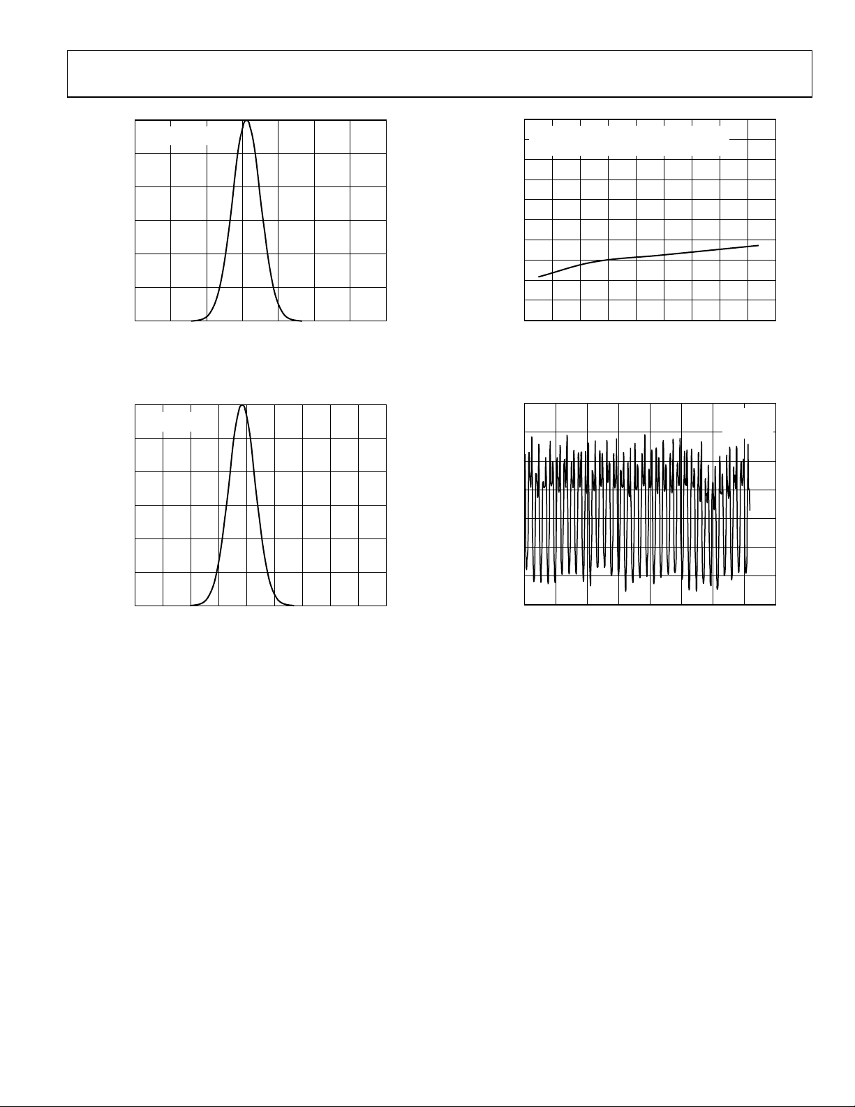
AD5934
30
MEAN = 0.1982
SIGMA = 0.0008
25
20
15
10
NUMBER OF DEVICES
5
0
0.192 0.194 0.196 0.198 0.200 0.202 0.204 0.206
VOLTAGE (V)
Figure 10. Range 4: Output Excitation Voltage Distribution VDD = 3.3 V
30
MEAN = 0.1792
SIGMA = 0.0024
25
20
15
10
NUMBER OF DEVICES
5
05325-070
15.8
AVDD1, AVDD2, DVDD CONNECTED TOGETHER.
15.3
14.8
14.3
13.8
13.3
IDD (mA)
12.8
12.3
11.8
11.3
10.8
OUTPUT EXCITATION FREQUENCY = 30kHz
RFB, Z
CALIBRATION
0
246810121416
= 100kΩ
MCLK FREQUENCY (MHz)
Figure 12. Typical Supply Current vs. AD5934 Clock Frequency
PHASE ERROR (Degrees)
0.4
0.2
0
–0.2
–0.4
–0.6
–0.8
VDD = 3.3V
T
A
f = 32kHz
= 25°C
18
05325-088
0
0.160
0.165 0.170 0.175 0.180 0.185 0.190 0.195 0.200
VOLTAGE (V)
Figure 11. Range 4: DC Bias Distribution VDD = 3.3 V
0.205
05325-075
–1.0
0
50 100 150 200 250 300 350
PHASE (Degrees)
Figure 13. Typical AD5934 Phase Error
400
05325-028
Rev. 0 | Page 9 of 32

AD5934
TERMINOLOGY
Tot a l S ys t em A cc ur ac y
The AD5934 can accurately measure a range of impedance
values to less than 0.5% of the correct impedance value for
supply voltages between 2.7 V to 5.5 V.
Signal-to-Noise Ratio (SNR)
SNR is the ratio of the rms value of the measured output signal
to the rms sum of all other spectral components below the
Nyquist frequency. The value for SNR is expressed in decibels.
Spurious-Free Dynamic Range
(SFDR)
Along with the frequency of interest, harmonics of the
fundamental frequency and images of these frequencies are
present at the output of a DDS device. The spurious-free
dynamic range refers to the largest spur or harmonic present in
the band of interest. The wideband SFDR gives the magnitude
of the largest harmonic or spur relative to the magnitude of the
fundamental frequency in the 0 to Nyquist bandwidth. The
narrow-band SFDR gives the attenuation of the largest spur
or harmonic in a bandwidth of ±200 kHz, about the
fundamental frequency.
Total Harmonic Distortion (THD)
THD is the ratio of the rms sum of harmonics to the
fundamental, where V1 is the rms amplitude of the
fundamental and V2, V3, V4, V5, and V6 are the rms
amplitudes of the second through the sixth harmonics.
For the AD5934, THD is defined as
2
2222
++++
VVVVV
6
THD
=
log20)db(
32
54
V
1
Rev. 0 | Page 10 of 32
 Loading...