

Serial Input 16-Bit
V
FEATURES
4 mA–20 mA, 0 mA–20 mA or 0 mA–24 mA
current output
16-bit resolution and monotonicity
±0.012% max integral nonlinearity
±0.05% max offset (trimmable)
±0.15% max total output error (trimmable)
Flexible serial digital interface (3.3 MBPS)
On-Chip loop fault detection
On-chip 5 V reference (25 ppm/°C max)
Asynchronous CLEAR function
Maximum power supply range of 32 V
Output loop compliance of 0 V to V
24-Lead SOIC and PDIP packages
GENERAL DESCRIPTION
The AD420 is a complete digital to current loop output
converter, designed to meet the needs of the industrial control
market. It provides a high precision, fully integrated, low cost
single-chip solution for generating current loop signals in a
compact 24-lead SOIC or PDIP package.
The output current range can be programmed to 4 mA to
20 mA, 0 mA to 20 mA or to an overrange function of 0 mA to
24 mA. The AD420 can alternatively provide a voltage output from
a separate pin that can be configured to provide 0 V to 5 V, 0 V
to 10 V, ±5 V, or ±10 V with the addition of a single external
buffer amplifier.
The 3.3 M Baud serial input logic design minimizes the cost of
galvanic isolation and allows for simple connection to commonly
used microprocessors. It can be used in 3-wire or asynchronous
mode and a serial-out pin is provided to allow daisy chaining of
multiple DACs on the current loop side of the isolation barrier.
The AD420 uses sigma-delta (Σ-Δ) DAC technology to achieve
16-bit monotonicity at very low cost. Full-scale settling to 0.1%
occurs within 3 ms. The only external components that are
required (in addition to normal transient protection circuitry)
are two low cost capacitors which are used in the DAC output filter.
If the AD420 is used at extreme temperatures and supply
voltages, an external output transistor can be used to minimize
power dissipation on the chip via the BOOST pin. The FAULT
DETECT pin signals when an open circuit occurs in the loop.
The on-chip voltage reference can be used to supply a precision
+5 V to external components in addition to the AD420 or, if the
Rev. H
Information furnished by Analog Devices is believed to be accurate and reliable. However, no
responsibility is assumed by Anal og Devices for its use, nor for any infringements of patents or ot her
rights of third parties that may result from its use. Specifications subject to change without notice. No
license is granted by implication or otherwise under any patent or patent rights of Analog Devices.
Trademarks and registered trademarks are the property of their respective owners.
− 2.75 V
CC
4 mA–20 mA, 0 mA–20 mA DAC
AD420
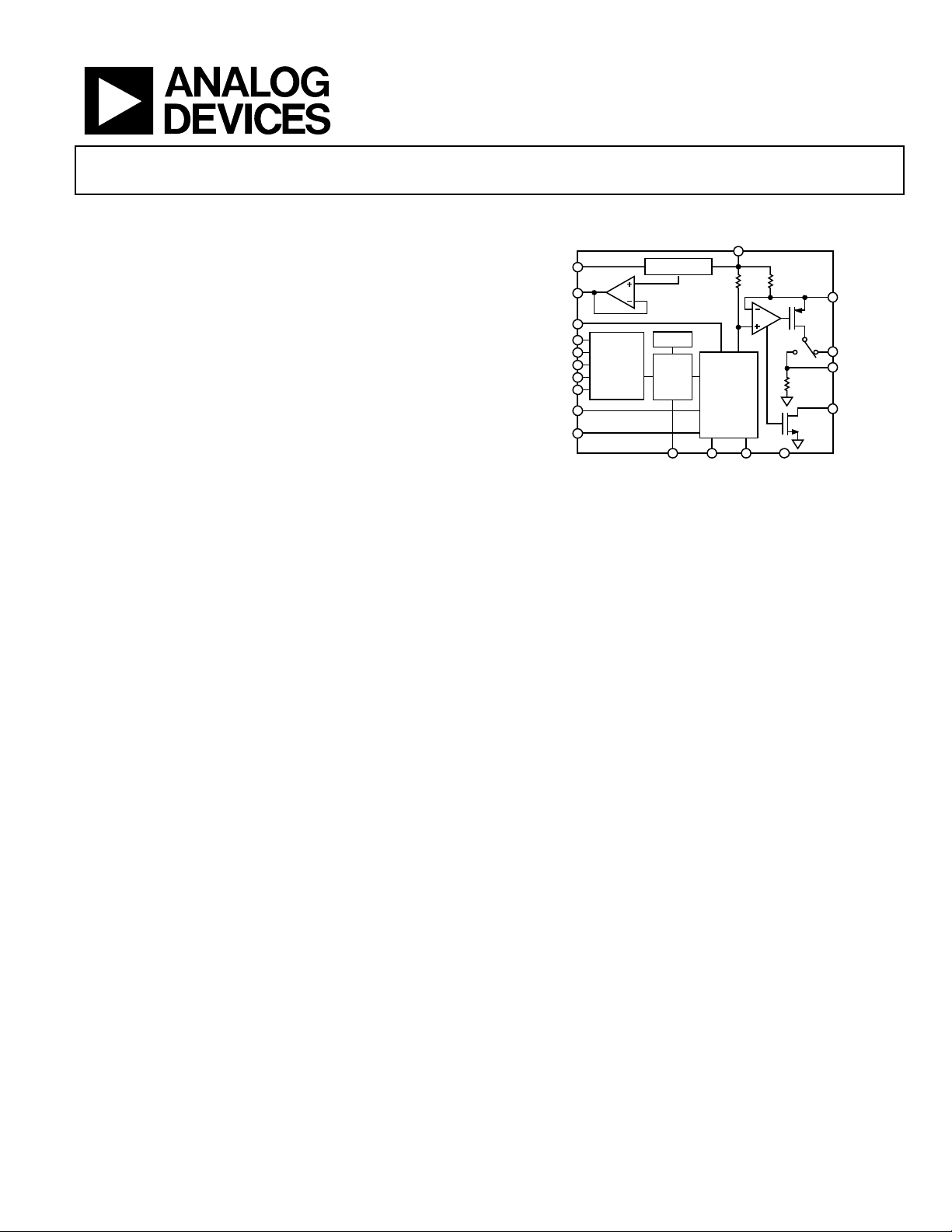
FUNCTIONAL BLOCK DIAGRAM
CC
V
LL
REF OUT
REF IN
DATA OUT
CLEAR
LATCH
CLOCK
DATA IN
RANGE
SELECT 1
RANGE
SELECT 2
DATA I/P
REGISTER
user desires temperature stability exceeding 25 ppm/°C, an
external precision reference such as the AD586 can be used as
the reference. The AD420 is available in a 24-lead SOIC and
PDIP over the industrial temperature range of −40°C to +85°C.
PRODUCT HIGHLIGHTS
1. The AD420 is a single chip solution for generating 4 mA to
20 mA or 0 mA to 20 mA signals at the controller end of
the current loop.
2. The AD420 is specified with a power supply range from
12 V to 32 V. Output loop compliance is 0 V to V
3. The flexible serial input can be used in 3-wire mode
with SPI® or MICROWIRE® microcontrollers, or in
asynchronous mode, which minimizes the number of
control signals required.
4. The serial data out pin can be used to daisy chain any
number of AD420s together in 3-wire mode.
5. At power-up, the AD420 initializes its output to the low
end of the selected range.
6. The AD420 has an asynchronous CLEAR pin, which sends
the output to the low end of the selected range (0 mA, 4 mA,
or 0 V).
7. The AD420 BOOST pin accommodates an external
transistor to off-load power dissipation from the chip.
8. The offset of ±0.05% and total output error of ±0.15% can
be trimmed if desired, using two external potentiometers.
One Technology Way, P.O. Box 9106, Norwood, MA 02062-9106, U.S.A.
Tel: 781.329.4700 www.analog.com
Fax: 781.461.3113 ©1999–2011 Analog Devices, Inc. All rights reserved.
REFERENCE
AD420
CLOCK
16-BIT
DAC
OFFSET
TRIM
Figure 1.
4kΩ
SWITCHED
CURRENT
SOURCES
AND
FILTERING
CAP 1 CAP 2 GND
40Ω
1.25kΩ
− 2.75 V.
CC
BOOST
I
OUT
V
OUT
FAULT
DETECT
00494-001

AD420
TABLE OF CONTENTS
Features.............................................................................................. 1
Functional Block Diagram .............................................................. 1
General Description ......................................................................... 1
Product Highlights ........................................................................... 1
Revision History ............................................................................... 2
Specifications..................................................................................... 3
Absolute Maximum Ratings............................................................ 5
ESD Caution.................................................................................. 5
Pin Configuration and Function Descriptions............................. 6
Timing Requirements ...................................................................... 7
Three-Wire Interface ................................................................... 7
Three-Wire Interface Fast Edges on Digital Input................... 7
Asynchronous Interface............................................................... 7
Terminology ...................................................................................... 8
Theory of Operation ........................................................................ 9
Applications Information .............................................................. 10
Current Output........................................................................... 10
Driving Inductive Loads............................................................ 10
Voltage-Mode Output................................................................ 10
Optional Span and Zero Trim .................................................. 10
Three-Wire Interface ................................................................. 11
Using Multiple DACS with Fault Detect ................................. 11
Asynchronous Interface Using Optocouplers ........................ 11
Microprocessor Interface............................................................... 12
AD420-To-MC68HC11 (SPI Bus) Interface........................... 12
AD420 to Microwire Interface ................................................. 12
External Boost Function ........................................................... 13
AD420 Protection........................................................................... 14
Transient Voltage Protection .................................................... 14
Board Layout And Grounding ................................................. 14
Power Supplies and Decoupling............................................... 14
Outline Dimensions....................................................................... 15
Ordering Guide .......................................................................... 15
REVISION HISTORY
1/11—Rev. G to Rev. H
Changes to Figure 13...................................................................... 13
Changes to Ordering Guide.......................................................... 15
11/09—Rev. F to Rev. G
Updated Format..................................................................Universal
Changes to Table 2............................................................................ 5
Updated Outline Dimensions....................................................... 15
Changes to Ordering Guide.......................................................... 15
9/99—Rev. E to Rev. F
Rev. H | Page 2 of 16

AD420
SPECIFICATIONS
TA = T
Table 1.
AD420-32 Version
Parameter Min Typ Max Units Comments
RESOLUTION 16 Bits
I
OUT
V
OUT
VOLTAGE REFERENCE
DIGITAL INPUTS
DIGITAL OUTPUTS
− T
MIN
CHARACTERISTICS RL = 500 Ω
Operating Current Ranges 4 20 mA
0 20 mA
0 24 mA
Current Loop Voltage Compliance 0 VCC − 2.75 V V
Settling Time (to 0.1% of FS)1 2.5 3 ms
Output Impedance (Current Mode) 25 MΩ
Accuracy2
Monotonicity 16 Bits
Integral Nonlinearity ±0.002 ±0.012 %
Offset (0 mA or 4 mA) (TA = +25°C) ±0.05 %
Offset Drift 20 50 ppm/° C
Total Output Error (20 mA or 24 mA) (TA = +25°C) ±0.15 %
Total Output Error Drift 20 50 ppm/° C
PSRR3 5 10 μA/V
CHARACTERISTICS
FS Output Voltage Range (Pin 17) 0 5 V
REF OUT
Output Voltage (TA = +25° C) 4.995 5.0 5.005 V
Drift ±25 ppm/° C
Externally Available Current 5 mA
Short Circuit Current 7 mA
REF IN
Resistance 30 kΩ
VLL
Output Voltage 4.5 V
Externally Available Current 5 mA
Short Circuit Current 20 mA
VIH (Logic 1) 2.4 V
VIL (Logic 0) 0.8 V
IIH (VIN = 5.0 V) ±10 μA
IIL (VIN = 0 V) ±10 μA
Data Input Rate (3-Wire Mode) No Minimum 3.3 MBPS
Data Input Rate (Asynchronous Mode) No Minimum 150 kBPS
FAU LT D EFEC T
VOH (10 kΩ Pull-Up Resistor to VLL) 3.6 4.5 V
VOL (10 kΩ Pull-Up Resistor to VLL) 0.2 0.4 V
VOL @ 2.5 mA 0.6 V
DATA OUT
VOH (IOH = −0.8 mA) 3.6 4.3 V
VOL (IOL = 1.6 mA) 0.3 0.4 V
, VCC = +24 V, unless otherwise noted.
MAX
Rev. H | Page 3 of 16

AD420
AD420-32 Version
Parameter Min Typ Max Units Comments
POWER SUPPLY
Operating Range VCC 12 32 V
Quiescent Current 4.2 5.5 mA
Quiescent Current (External VLL) 3 mA
TEMPERATURE RANGE
Specified Performance −40 +85 °C
1
External capacitor selection must be as described in Figure 6.
2
Total Output Error includes Offset and Gain Error. Total Output Error and Offset Error are with respect to the Full-Scale Output and are measured with an ideal +5 V
reference. If the internal reference is used, the reference errors must be added to the Offset and Total Output Errors.
3
PSRR is measured by varying VCC from 12 V to its maximum 32 V.
Rev. H | Page 4 of 16
AD420
ABSOLUTE MAXIMUM RATINGS
Table 2.
Parameter Rating
VCC to GND 32 V
I
to GND VCC
OUT
Digital Inputs to GND −0.5 V to +7 V
Digital Output to GND −0.5 V to VLL + 0.3 V
VLL and REF OUT: Outputs Safe for
Indefinite Short to Ground
Storage Temperature −65°C to +150°C
Lead Temperature (Soldering, 10 sec) +300°C
Lead Temperature, Soldering Reflow +260°C
Thermal Impedance:
SOIC (R) Package θJA = 75°C/W
PDIP (N) Package θJA = 50°C/W
Stresses above those listed under Absolute Maximum Ratings
may cause permanent damage to the device. This is a stress
rating only; functional operation of the device at these or any
other conditions above those indicated in the operational
section of this specification is not implied. Exposure to absolute
maximum rating conditions for extended periods may affect
device reliability.
Table 3. Truth Table
Inputs
Range
CLEAR
0 X X Normal operation
1 X X
X 0 0 0 V–5 V range
X 0 1 4 mA–20 mA range
X 1 0 0 mA–20 mA range
X 1 1 0 mA–24 mA range
Select 2
Range
Select 1 Operation
Output at bottom of
span
ESD CAUTION
Rev. H | Page 5 of 16
 Loading...