High Definition Audio
ADC0
ADC1
DAC0
DM_CLK
DM_1/2
DM_2
DIGITAL
MICROPHONE
MONO OUT
PORT A
PORT D
PORT F
AD1984A
H
D
A
U
D
I
O
I
N
T
E
R
F
A
C
E
PORT B
PORT E
PORT C
DAC1
⌺
⌺
⌺
⌺
⌺
PCBEEP
HP
HP
⌺
DIGITAL
PCBEEP
S/PDIF
www.BDTIC.com/ADI
SoundMAX Codec
AD1984A
FEATURES
Microsoft Vista Premium Logo for desktop
96+ dB audio outputs, 90 dB audio inputs
WLP 3.0 and 4.0
Security feature prevents unauthorized recording
2 stereo headphone amplifiers
Internal 32-bit arithmetic for greater accuracy
Impedance and presence detection on all jacks
Full analog mixer with DAC inputs
3 independent microphone bias pins
Digital and analog PCBeep
3 general-purpose digital I/O (GPIO) pins
3.3 V analog supply voltage
1.7 V to 1.9 V or 3.3 V digital supply voltages
1.5 V or 3.3 V HD Audio link signaling voltage
Advanced power management modes
48-lead, RoHS compliant LFCSP_VQ package
192 kHz DACs/ADCs
2 independent stereo DAC/ADC pairs
Simultaneous record of 2 stereo channels
Simultaneous playback of 2 stereo channels
Independent 8 kHz, 11.025 kHz, 16 kHz, 22.05 kHz, 32 kHz,
44.1 kHz, 48 kHz, 88.2 kHz, 96 kHz, 176.4 kHz, and 192 kHz
sample rates
16-, 20-, and 24-bit resolution
Selectable stereo mixer on outputs
STEREO DIGITAL MICROPHONE INTERFACE
Two 192 kHz digital microphone channels
Supports 1 or 2 microphones per pin
Selectable bit clock rates of 1.5 MHz, 2.0 MHz, and 3.0 MHz
Mono and stereo array support
8 kHz, 11.025 kHz, 16 kHz, 22.05 kHz, 32 kHz, 44.1 kHz,
48 kHz, 88.2 kHz, 96 kHz, 176.4 kHz, and 192 kHz
sample rates
16-, 20-, and 24-bit resolution
S/PDIF OUTPUT
Supports 44.1 kHz, 48 kHz, 88.2 kHz, 96 kHz, 176.4 kHz, and
192 kHz sample rates
16-, 20-, and 24-bit data; PCM and AC3 formats
Digital PCM gain control
AUXILIARY PINS
Stereo CD/auxiliary I/O port with ground sense
Stereo auxiliary/dock I/O port
Mono out pin for internal speakers or telephony
Rev. 0
Information furnished by Analog Devices is believed to be accurate and reliable.
However, no responsibility is assumed by Analog Devices for its use, nor for any
infringements of patents or other rights of third parties that may result from its use.
Specifications subject to change without notice. No license is granted by implication
or otherwise under any patent or patent rights of Analog Devices. Trademarks and
registered trademarks are the property of their respective owners.
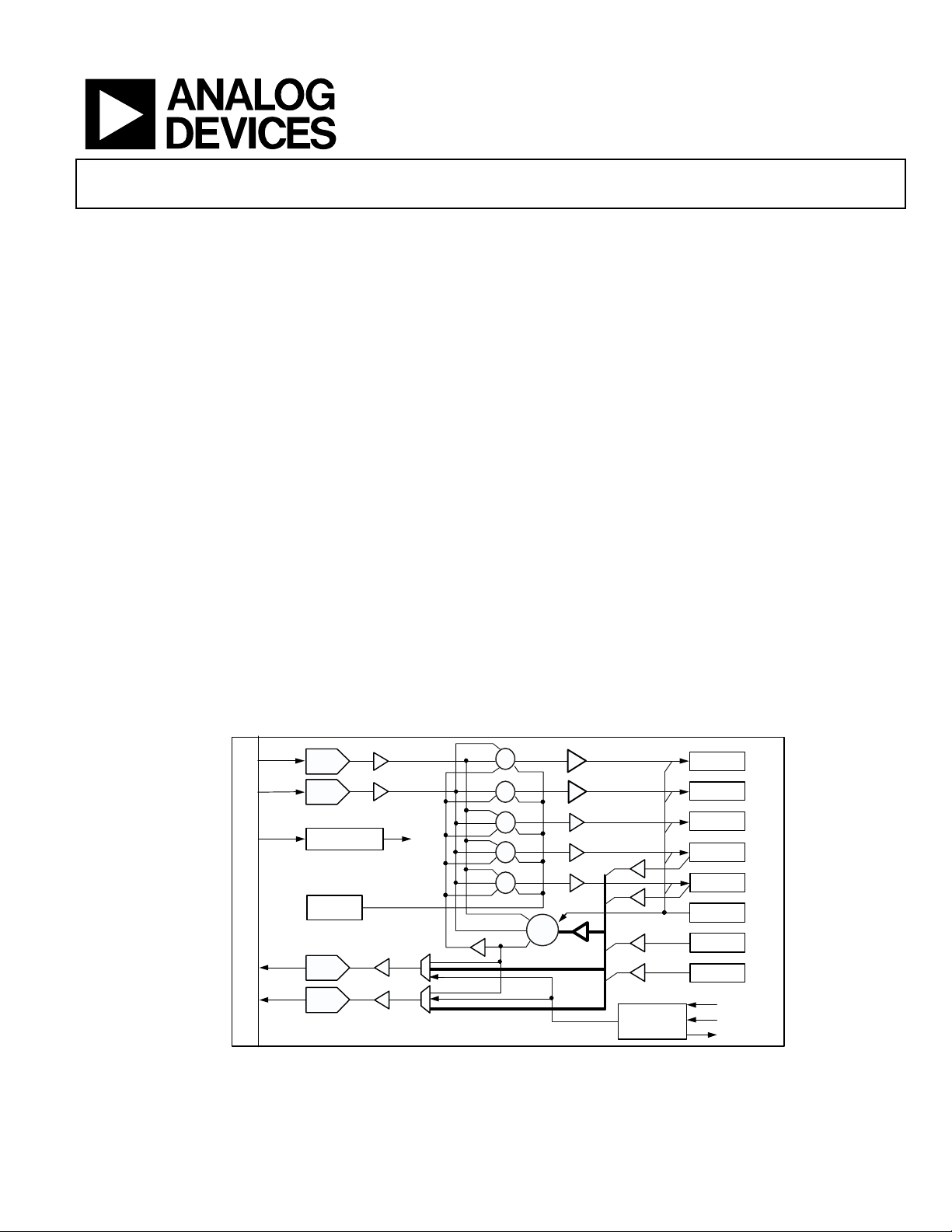
Figure 1. Functional Block Diagram
One Technology Way, P.O. Box 9106, Norwood, MA 02062-9106 U.S.A.
Tel: 781.329.4700 www.analog.com
Fax: 781.461.3113 ©2008 Analog Devices, Inc. All rights reserved.

AD1984A
www.BDTIC.com/ADI
TABLE OF CONTENTS
Features ................................................................. 1
Revision History ...................................................... 2
General Description ................................................. 3
Additional Information .......................................... 3
Jack Configuration ................................................ 3
AD1984A Specifications ............................................ 4
Test Conditions .................................................... 4
Performance ........................................................ 4
General Specifications ............................................ 4
HD Audio Link Specification ................................... 7
Power-Down States ............................................... 7
Absolute Maximum Ratings .................................... 8
ESD Caution ........................................................ 8
Environmental Conditions ...................................... 8
Pin Configuration and Function Descriptions ................. 9
Digital Microphone Interface Timing Specifications ....... 12
HD Audio Widgets ................................................ 14
HD Audio Parameters ............................................. 15
Widget Parameters ................................................. 16
Connection List ..................................................... 17
Default Configuration Bytes ..................................... 18
Outline Dimensions ............................................... 19
Ordering Guide ..................................................... 19
REVISION HISTORY
4/08—Rev 0. Initial version
Rev. 0 | Page 2 of 20 | April 2008

GENERAL DESCRIPTION
www.BDTIC.com/ADI
AD1984A
The AD1984A audio codec and SoundMAX® software provide
superior high definition audio quality that exceeds Vista Premium performance. The AD1984A has two 192 kHz DAC pairs,
two 192 kHz ADC pairs, an S/PDIF output, a 2-channel digital
microphone interface, and digital and analog PCBeep. These
features make the AD1984A the right choice for desktop and
notebook PCs where performance is key.
The AD1984A is available in a 48-lead, RoHS compliant lead
frame chip scale package in both reels and trays. See Ordering
Guide on Page 19.
ADDITIONAL INFORMATION
This data sheet provides a general overview of the AD1984A
SoundMAX codec’s architecture and functionality. Detailed
widget information is available in the AD1984A Programmers
Reference Manual. Please contact your local Analog Devices,
Inc., sales representative for more information.
JACK CONFIGURATION
The guidelines shown in Table 1 through Table 3 should be
used when selecting ports for particular functions.
Table 1. Typical Desktop Configuration
Port Function
Port A Front Panel Headphone
Port B Front Panel Microphone
Port C Rear Panel Line-In/Microphone
Port D Rear Panel Line-Out/Headphone
S/PDIF Optical/RCA S/PDIF Output
Table 3. Typical Notebook Configuration with Dock
Interface
Port Function
Port A Headphone
Port B Microphone
Port C Internal Microphone
Port D Dock Line-Out/Headphone
Port E Dock Line-In/Microphone
Port F Internal Stereo Speakers
S/PDIF Optical/RCA S/PDIF Output
Table 2. Typical Notebook Configuration
Port Function
Port A Headphone
Port B Microphone
Port C Internal Microphone
Port F Internal Stereo Speakers
S/PDIF Optical/RCA S/PDIF Output
Rev. 0 | Page 3 of 20 | April 2008

AD1984A
www.BDTIC.com/ADI
AD1984A SPECIFICATIONS
TEST CONDITIONS
Parameter Test Condition
Tem pe ra tu re
Digital Supply
Analog Supply
MIC_BIAS_IN (via Low-Pass Filter)
Sample Rate F
S
Input Signal (Frequency Sine Wave)
Amplitude for THD + N
Analog Output Pass Band
1
DAC
ADC 0 dB Gain
1
DAC/ADC tests are performed with AES-17 filter enabled.
PERFORMANCE
Parameter Min Typ Max Unit
Line-Out Drive (10 kΩ loads—DAC to Pin)
Total Harmonic Distortion (THD + N)
Dynamic Range (–60 dB in ref to fS A-Weighted)
Signal-to-Noise Ratio
Headphone Drive (32 Ω loads—DAC to Pin)
Total Harmonic Distortion (THD + N)
Dynamic Range (–60 dB in ref to f
Signal-to-Noise Ratio
Microphone/Line-In (Pin to ADC, Mic Boost = 0 dB)
Total Harmonic Distortion (THD + N)
Dynamic Range (–60 dB in ref to f
Signal-to-Noise Ratio
A-Weighted)
S
A-Weighted)
S
25°C
3.3 V
3.3 V
5.0 V
48 kHz
1008 Hz
–3.0 dB Full Scale
20 Hz to 20 kHz
10 kΩ Output Load: Line-Out Tests
32 Ω Output Load: Headphone Tests
–86
96
96
–80
96
96
–81
90
90
dB
dB
dB
dB
dB
dB
dB
dB
dB
GENERAL SPECIFICATIONS
Parameter Min Typ Max Unit
DIGITAL DECIMATION AND INTERPOLATION FILTERS—f
= 8 kHz to 192 kHz
S
Pass Band 0 0.4 f
Pass-Band Ripple ±0.005 dB
Stop Band 0.6 f
Stop-Band Rejection –100 dB
Group Delay 20 1/f
Group Delay Variation over Pass Band 0 μs
ANALOG-TO-DIGITAL CONVERTERS
Resolution 24 Bits
Gain Error (Full-Scale Span Relative to Nominal Input Voltage) ±10 %
Interchannel Gain Mismatch (Difference of Gain Errors) ±0.2 ±0.5 dB
ADC Offset Error
ADC Crosstalk
1
1
Line Inputs (Input L, Ground R, Read R; Input R, Ground L, Read L) –85 dB
Line Inputs to Other –100 –80 dB
Rev. 0 | Page 4 of 20 | April 2008
1
S
S
Hz
Hz
±5mV
S

AD1984A
www.BDTIC.com/ADI
Parameter Min Typ Max Unit
DIGITAL-TO-ANALOG CONVERTERS
Resolution 24 Bits
Gain Error (Full-Scale Span Relative to Nominal Input Voltage)
Interchannel Gain Mismatch (Difference of Gain Errors) ±0.5 dB
Total Audible Out-of-Band Energy (Measured from 0.6 × fS to 20 kHz)
DAC Crosstalk (Input L, Zero R, Measure R_OUT; Input R, Zero L, Measure L_OUT)
DAC VOLUMES
Step Size 1.5 dB
Output Gain/Attenuation Range –58.5 0 dB
Mute Attenuation of 0 dB Fundamental
1
ADC VOLUMES
Step Size 1.5 dB
PGA Gain/Attenuation Range –58.5 +22.5 dB
ANALOG MIXER
Signal-to-Noise Ratio Input to Output—Ports B, C, E, or F to Port D Output 95 dB
Step Size: All Mixer Inputs –1.5 dB
Input Gain/Attenuation Range: All Mixer Inputs –34.5 +12.0 dB
ANALOG LINE LEVEL OUTPUTS
Full-Scale Output Voltage 1.0
Ports A, D, E, F, and Mono Out
Output Impedance
External Load Impedance
Output Capacitance
External Load Capacitance 1000 pF
ANALOG HP DRIVE OUTPUTS
Full-Scale Output Voltage 1.0
Ports A and D
Output Impedance
External Load Impedance
Output Capacitance
External Load Capacitance
ANALOG INPUTS
Input Voltages—Ports B, C, E, or F
Mic Boost = 0 dB 1
Input Voltages—Microphone Boost
Mic Boost = 10 dB 0.316
Amplifier, Ports B, C, or E
Mic Boost = 20 dB 0.1
Mic Boost = 30 dB 0.032
Input Impedance
PCBeep
Ports B, C, E (Mic Boost = 0 dB)
Port F
Input Capacitance
1
1
1
1
–85 dB
–95 dB
±10 %
–80 dB
V rms
2.83
1
1
1
10 kΩ
190 Ω
15 pF
V p-p
V rms
2.83
1
1
1
1
32 Ω
15 pF
0.5 Ω
1000 pF
V p-p
V rms
2.83
V p-p
V rms
0.894
V p-p
V rms
0.283
V p-p
V rms
0.089
23
150
45
V p-p
kΩ
kΩ
kΩ
57.5pF
Rev. 0 | Page 5 of 20 | April 2008

AD1984A
www.BDTIC.com/ADI
Parameter Min Typ Max Unit
MICROPHONE BIAS
MIC_BIAS-B, MIC_BIAS-C
MIC_BIAS_IN (Pin 33) = 5 V or 3.3 V V
V
MIC_BIAS_IN (Pin 33) = 5 V V
V
MIC_BIAS_IN (Pin 33) = 3.3 V V
Setting = High-Z High-Z
REF
V
Setting = 0 V 0 V dc
REF
Setting = 50% 1.65 V dc
REF
Setting = 80% 3.7 V dc
REF
Setting = 100% 3.9 V dc
REF
Setting = 80% 2.86 V dc
REF
V
Setting = 100% 3.0 V dc
REF
MIC_BIAS-E (When Enabled as BIAS) V
Output Drive Current V
Setting = High-Z High-Z
REF
Setting = 0 V 0 V dc
V
REF
V
Setting = 50% 1.65 V dc
REF
Setting = 80% 2.86 V dc
V
REF
V
Setting = 100% 3.0 V dc
REF
Setting = 50%, 80%, or 100% 1.6 mA
REF
GPIO 0
Input Signal High (VIH)DV
Input Signal Low (V
Output Signal High ( V
Output Signal Low (V
Input Leakage Current (Signal High) (I
Input Leakage Current (Signal Low) (I
)0DV
IL
) I
OH
)I
OL
IH
)–50μA
IL
= –500 μADV
OUT
= +1500 μA0DV
OUT
) 150 nA
× 0.60 DV
IO
× 0.72 DV
IO
IO
× 0.24 V
IO
IO
× 0.10 V
IO
V
V
GPIO 1 and GPIO 2
Input Signal High (VIH)AV
Input Signal Low (V
Output Signal High ( V
Output Signal Low (V
Input Leakage Current (Signal High) (I
Input Leakage Current (Signal Low) (I
)0AV
IL
)I
OH
)I
OL
IH
)–50μA
IL
= –500 μAAV
OUT
= +1500 μA0AV
OUT
) 150 nA
× 0.60 AV
DD
× 0.72 AV
DD
DD
× 0.24 V
DD
DD
× 0.10 V
DD
V
V
DM Clock
Output Signal High ( VOH)I
Output Signal Low (V
)I
OL
= –500 μAAV
OUT
= +1500 μA0AV
OUT
× 0.72 AV
DD
DD
× 0.10 V
DD
V
DM_1/2 and DM_2
Input Signal High (V
Input Signal Low (V
)AV
IH
)0AV
IL
Input Leakage Current (Signal High) (I
Input Leakage Current (Signal Low) (I
) –150 nA
IH
)–50nA
IL
× 0.60 AV
DD
DD
× 0.24 V
DD
V
S/PDIF
Input Signal High (V
Input Signal Low (V
Output Signal High ( V
Output Signal Low (V
)DV
IH
)0DV
IL
) I
OH
)I
OL
Input Leakage Current (Signal High) (I
Input Leakage Current (Signal Low) (I
= –500 μADV
OUT
= +1500 μA0DV
OUT
) 150 nA
IH
)–50μA
IL
× 0.60 DV
IO
× 0.72 DV
IO
IO
× 0.24 V
IO
IO
× 0.10 V
IO
V
V
Rev. 0 | Page 6 of 20 | April 2008
 Loading...