

PRELIMINARY TECHNICAL DATA
r
I
C I
C
r
a High Performance Multibit Σ∆
Σ∆ DAC
Σ∆Σ∆
with SACD Playback
Preliminary Technical Data AD1955
FEATURES
5V Power Supply Stereo Audio DAC System.
Accepts 16/18/20/24-Bit Data
Supports 24-Bits, 192kHz Sample Rate PCM Audio Data
Supports SACD bit-stream and External Digital Filter Interface
Accepts a Wide Range of PCM Sample Rates Including:
32kHz, 44.1kHz. 48kHz, 88.2kHz, 96kHz, and 192kHz
Multibit Sigma Delta Modulator with “Perfect Differential
Linearity Restoration” for Reduced Idle Tones and Noise Floor
Data Directed Scrambling DAC - Least Sensitive to Jitter
Supports SACD playback with “Bit Expansion” filter
Differential Current Output for Optimum Performance
8.64 mA p-p Output Current with +3dB headroom in SACD mode
120 dB SNR/DNR (not muted) at 48KHz Sample Rate
(A-Weighted Stereo)
123 dB SNR/DNR (Mono)
-110 dB THD+N
110 dB Stopband Attenuation with +/-0.0002dB Passband Ripple
8 Times Oversampling Digital Filter
On-chip Clickless Volume Control
Supports SACD-Mute pattern detection
Supports 64fs/128fs DSD SACD with phase modulation
Internal Digital Filter pass-through for External Filter
Master clock: 256fs,384fs,512fs,768fs
Hardware and Software Controllable Clickless Mute
Serial (SPI) Control for: Serial Mode, Number of Bits,
Sample Rate, Volume, Mute, De-emphasis, Mono Mode
Digital De-emphasis for 32, 44.1, 48 KHz Sample Rates
Flexible Serial Data Port with Right-Justified, Left-Justified,
2
I
S-Compatible and DSP Serial Port
28 Lead SSOP Plastic Package
APPLICATIONS
High-End DVD-Audio, SACD, CD, Home Theatre Systems, Automotive
Audio Systems, Sampling Musical Keyboards, Digital Mixing
Consoles, Digital Audio Effects Processors
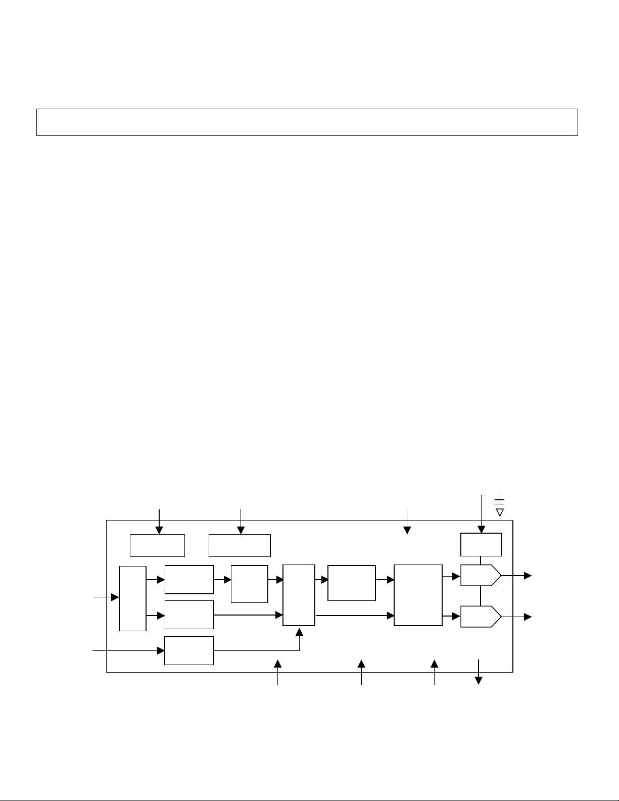
PRODUCT OVERVIEW
The AD1955 is a complete high performance single-chip stereo digital
audio playback system. It is comprised of a multibit sigma-delta
modulator, high performance digital interpolation filters, and continuoustime differential current output DAC section. Other features include an
on-chip clickless stereo attenuator, mute capability, programmed through
an SPI-compatible serial control port. The AD1955 is fully compatible
with all known DVD audio formats including 192kHz as well as 96kHz
sample frequencies and 24-bits. It also is backwards compatible by
supporting 50/15µs digital de-emphasis intended for “redbook” Compact
Discs, as well as de-emphasis at 32kHz and 48kHz sample rate.
The AD1955 has a very flexible serial data input port that allows for
glueless interconnection to a variety of ADCs, DSPs, SACD decoder,
external digital filter, AES/EBU receivers and sample rate converters.
The AD1955 can be configured in Left-justified, I
2
S, Right-Justified, or
DSP serial port compatible modes. It can support MSB first, twoscompliment format, 16, 18, 20 and 24 bits in all standard PCM modes.
Also the AD1955 has an interface for SACD playback and an external
digital filter interface for use with an external digital interpolation filter
or HDCD decoder. The AD1955 uses a +5 V power supply. It is
fabricated on a single monolithic integrated circuit and is housed in a 28pin SSOP package for operation over the temperature range -40
0
+105
C.
0
C to
FUNCTIONAL BLOCK DIAGRAM
16/20/24Bit
Audio Data /
External Digital
Filter Input
Bitstream
DSD
Input
3 / 4
4
Master Clock
Input
Auto-Clock
Divider
M
U
X
Serial Data
Interface
External
Filter I/F
DSD
Filte
Control Data
Input
SPI
Control
Digital
Filter
Engine
3
S/H
Multibit
Sigma-Delta
Modulato
Rev. PrF 3/18/2002
Information furnished by Analog Devices is believed to be accurate and
reliable. However, no responsibility is assumed by Analog Devices for its use;
nor for any infringements of patents or other rights of third parties which may
result from its use. No license is granted by implication or otherwise under
any patent or patent rights of Analog Devices.
One Technology Way, P.O. Box 9106, Norwood, MA 02062-9106 U.S.A.
Tel: 781/329-4700 www.analog.com
Fax: 781/326-8703 ©Analog Devices, Inc., 2002
Digital
Supply
Noise-
Shaped
Scrambling
Analog
Supply
Voltage
Reference
-DA
-DA
ZERO FlagsMUTERESET
L-ch
Differential
Current Output
R-ch

PRELIMINARY TECHNICAL DATA
AD1955
TEST CONDITIONS UNLESS OTHERWISE NOTED
Analog Supply Voltages (AVDD) +5.0V
Digital Supply Voltages (DV
Reference Current (Iref) .960 mA
Ambient Temperature 25
Input Clock 12.288 MHz
Input Signal 996.11 Hz
0 dB Full Scale
Input Sample Rate 48 kHz
Measurement Bandwidth 20 Hz to 20KHz
Word Width 24 Bits
Load Capacitance 100 pF
Load Impedance 47 k ohms
Input Voltage HI 2.4 V
Input Voltage LO .8 V
ANALOG PERFORMANCE (See Figures ) Iref = .960 mA
Min Typ Max Units
Resolution
Signal-to-noise Ratio (20 Hz to 20kHz)
Differential Output (A-weighted, RMS) (Stereo) 120 dB
Differential Output (A-weighted, RMS) (Mono) 123 dB
Single-ended (Stereo) 119 dB
Dynamic Range (20 Hz to 20 kHz, -60 dB Input)
Differential Output (A-weighted, RMS) (Stereo) 120 dB
Differential Output (A-weighted, RMS) (Mono) 123 dB
Single-ended (Stereo) 119 dB
Total Harmonic Distortion + Noise (Stereo) at 0 dBFS -108 dB
Analog Outputs
Differential Output range (Full Scale) 8.64 mA p-p
Output Capacitance at Each Output Pin 100 pF
Output bias current, Each Output -3.24 mA
Out-of-Band Energy (0.5XFs to 100 kHz) -90 dB
Reference Voltage 2.39 V
DC Accuracy
Gain Error +/-3 %
Interchannel Gain Mismatch 0.01 dB
Gain Drift 25 ppm/OC
Interchannel Crosstalk (EIAJ method) -125 dB
Interchannel Phase Deviation +/- 0.1 Degrees
Mute Attenuation -100 dB
De-emphasis Gain Error +/- 0.1 dB
NOTES:
Performance of right and left channels are identical (exclusive of the Interchannel Gain Mismatch and Interchannel Phase Deviation specifications).
DIGITAL I/O (-40oC to 105oC)
Min
Input Voltage HI (VIH) 2.0 V
Input Voltage LO (VIL) 0.8 V
Input Leakage (IIH@VIH=2.4 V) 10 uA
Input Leakage (IIL@VIL=0.8 V) 10 uA
High Level Output Voltage (VOH) IOH = 1 mA 2.4 V
Low Level Output Voltage (VOL) IOL = 1 mA 0.4 V
Input Capacitance 20 pF
Specifications subject to change without notice
) +5.0V
DD
O
C
Specifications subject to change without notice.
24
Typ
Max Units
Bits
-2- Rev. PrF

PRELIMINARY TECHNICAL DATA
AD1955
TEMPERATURE RANGE
Specifications Guaranteed 25
Functionality Guaranteed -40 105
Storage -55 125
Specifications subject to change without notice
POWER
Supplies
Voltage, Digital 4.50 5 5.50 V
Voltage, Analog 4.50 5 5.50 V
Analog Current 17 mA
Analog Current - Reset 17 mA
Digital Current 22 mA
Digital Current - Reset 2 mA
Dissipation
Operation - Both Supplies 195 mW
Operation - Analog Supply 85 mW
Operation - Digital Supply 110 mW
Power Supply Rejection Ratio
1kHz 300 mV p-p Signal at Analog Supply Pins -77 dB
20kHz 300 mV p-p Signal at Analog Supply Pins -72 dB
Specifications subject to change without notice
DIGITAL FILTER CHARACTERISTICS
Sample Rate (kHz) Passband (kHz) Stopband (kHz) Stopband Attenuation (dB) Passband Ripple (dB)
44.1 DC-20 24.1-328.7 110 +/- 0.0002
48 DC-21.8 26.23-358.28 110 +/- 0.0002
96 DC-39.95 56.9-327.65 115 +/- 0.0005
192 DC-87.2 117-327.65 95 +0/-0.04 (DC-21.8 kHz)
+0/-0.5 (DC-65.4 kHz)
+0/-1.5 (DC-87.2 kHz)
Specifications subject to change without notice
GROUP DELAY
Chip Mode
Group Delay Calculation Fs Group Delay Units
INT8x Mode 5553/(128 × FS) 48kHz 903.8
INT4x Mode 5601/(64 × FS) 96kHz 911.6
INT2x Mode 5659/(32 × FS) 192kHz 921
Specifications subject to change without notice
DIGITAL TIMING (Guaranteed over -40°C to 85°C, AVDD = DVDD = +5.0 V +/- 10%)
t
MCLK Period (FMCLK = 256*FLRCLK) 54 ns
DMP
t
MCLK LO Pulse Width (all modes) 0.4 X t
DML
t
MCLK HI Pulse Width (all modes) 0.4 X t
DMH
t
BCLK HI Pulse Width 20 ns
DBH
t
BCLK LO Pulse Width 20 ns
DBL
t
BCLK Period 60 ns
DBP
t
LRCLK Setup 20 ns
DLS
t
LRCLK Hold (DSP Serial Port mode only) 5 ns
DLH
t
SDATA Setup 5 ns
DDS
t
SDATA Hold 10 ns
DDH
t
CCLK Period 50 ns
DMP
t
CCLK LO Pulse Width 15 ns
DML
t
CCLK HI Pulse Width 15 ns
DMH
t
CLATCH Setup 10 ns
CLS
t
CLATCH Hold 10 ns
CLH
t
CDATA Setup 10 ns
CDS
t
CDATA Hold 10 ns
CDH
t
RST LO Pulse Width 15 ns
RSTL
Specifications subject to change without notice.
Min Typ Max Units
O
C
O
C
O
C
Min Typ Max Units
µs
µs
µs
Min
ns
DMP
ns
DMP
Units
Rev. PrF -3-

PRELIMINARY TECHNICAL DATA
K
K
A
A
K
A
R
A
AD1955
ABSOLUTE MAXIMUM RATINGS* PACKAGE CHARACTERISTICS
Min Max Units Min Typ Max Units
DVDD to DGND -0.3 6 V OJA (Thermal Resistance
[Junction-to-Ambient])
AVDD to AGND -0.3 6 V OJC (Thermal Resistance
[Junction-to-Case])
Digital Inputs DGND - 0.3 DVDD + 0.3 V
Analog Outputs AGND - 0.3 AVDD + 0.3 V
AGND to DGND -0.3 0.3 V
Reference Voltage (AVDD + 0.3)/2
Soldering +300 OC
10 sec
* Stresses greater than those listed under Absolute Maximum Ratings may cause
permanent damage to the device. This is a stress rating only; functional operation
of the device at these or any other conditions above those indicated in the
operational section of this specification is not implied. Exposure to absolute
maximum rating conditions for extended periods may affect device reliability.
ORDERING GUIDE
Model Temperature Package
AD1955YRS
AD1955YRSRL
*RS = Shrink Small Outline
-40
-40
O
C to +105
O
C to +105
O
C
O
C
Description
28-Lead SSOP
28-Lead SSOP
PIN CONFIGURATION
1
Package Option*
RS-28
RS-28 on 13”
Reels
28DVDD
DGND
109.0 OC/W
39.0 OC/W
EF_WCLK/LRCL
EF_BCLK/BCL
EF_LDATA/SDAT
EF_RDAT
DSD_SCL
DSD_LDAT
DSD_RDAT
DSD_PHAS E
AGND
IOUTR+
IOUTR-
FILT
IREF AVDD
2
3
4
5
6
7
8
9
10
11
12
13
14 15
27
26
25
24
23
22
21
20
19
18
17
16
MCLK
CCLK
CLATCH
CDATA
PD/RST
MUTE
ZEROL
ZEROR
AGND
IOUTL+
IOUTL-
FILTB
CAUTION
ESD (Electrostatic discharge) sensitive device. Electrostatic charges as high as 400 V readily
accumulate on the human body and Test equipment and can discharge without detection.
Although the AD1959 features proprietary ESD protection circuitry, permanent Damage may
occur on devices subjected to high energy electrostatic discharges. Therefore, proper ESD
precautions are recommended to avoid performance degradation or loss of functionality.
-4- Rev. PrF

PRELIMINARY TECHNICAL DATA
AD1955
PIN FUNCTION DESCRIPTIONS
Pin I/O Pin Name Description
1 DVDD Digital Power Supply Connected to Digital 5V supply.
2 Input EF_WCLK/LRCLK Word Clock in External Filter mode.
Left/Right Clock input for input data in PCM mode.
3 Input EF_BCLK/BCLK Bit Clock input in External Filter mode. Bit Clock input for input data in PCM mode.
4 Input EF_LDATA/SDATA 8fs or 4fs L-ch Data input in External filter mode. Data should be MSB first two’s
complement format. In the PCM mode, serial input, MSB first, containing two
channels(left and right) of 16 to 24bit two’s complement 1fs data.
5 Input EF_RDATA 8fs or 4fs R-ch Data input in External filter mode. Data should be MSB first two’s
complement format. Not used in PCM mode
6 I/O DSD_SCLK Shift clock input for DSD data. This clock should be 64x44.1kHz, 2.8224MHz or
128x44.1kHz, 5.6448MHz in normal mode or 128x44.1kHz, 5.6448MHz or
256x44.1kHz, 11.2896MHz in phase mode.
7 Input DSD_LDATA DSD Left channel data input
8 Input DSD_RDATA DSD Right channel data input
9 I/O DSD_PHASE DSD phase reference signal. This clock should be 64x44.1kHz, 2.8224MHz. If not
used this pin should be connected Low.
10 AGND Analog Ground
11 Output IOUTR+ Right Channel Positive analog output.
12 Output IOUTR- Right Channel Negative analog output.
13 Output FILTR Voltage Reference Filter Capacitor Connection. Bypass and decouple the voltage
reference with parallel 10uF and 0.1uF capacitors to AGND
14 IREF Connection point for external bias resistor.
15 AVDD Analog power supply Connected to Analog 5V supply
16 Output FILTB Filter Capacitor Connection with parallel 10uF and 0.1uF capacitors to AGND
17 Output IOUTL- Left Channel Negative analog output.
18 Output IOUTL+ Left Channel Positive analog output.
19 AGND Analog Ground
20 Output ZEROR Right Channel Zero Flag Output. This pin goes high when the right channel has no
signal input or the DSD mute pattern is detected.
21 Output ZEROL Left Channel Zero Flag Output. This pin goes high when the left channel has no signal
input or the DSD mute pattern is detected.
22 Input MUTE Mute. Assert HI to mute both stereo analog outputs. Deassert LO for normal
operation.
23 Input PD/RST Power down/Reset. The AD1955 is placed in a reset state and the digital circuitry is
powered down when this pin is held LO. The AD1955 is reset on the rising edge of
this signal. The serial control port registers are reset to the default values. Connect HI
for normal operation.
24 Input CDATA Serial control input, MSB first, containing 16 bits of unsigned data. Used for
specifying control information and channel-specific attenuation.
25 Input CLATCH Latch Input for control data.
26 Input CCLK Control Clock input for control data. Control input data must be valid on the rising
edge of CCLK. CCLK may be continuous or gated.
27 Input MCLK Master Clock Input. Connect to an external clock source.
28 DGND Digital Ground
Rev. PrF -5-

PRELIMINARY TECHNICAL DATA
AD1955
OPERATING FEATURES
Serial Data Input Port
The AD1955’s flexible serial data input port accepts standard PCM audio data and external digital filter output data in twoscomplement, MSB-first format in PCM/External digital filter mode and a dedicated SACD serial port accepts DSD bit-stream data in
SACD mode. If the PCM mode is selected by control register 0 bit12 and 13, the left channel data field always precedes the right
channel data field. The serial data format and word length in PCM mode are set by the mode select bits (bits 4 and 5 and bits 2 and 3,
respectively) in the SPI control register.
In all data formats except for the right-justified mode, the serial port will accept an arbitrary number of bits up to a limit of 24 (extra
bits will not cause an error, but they will be truncated internally). In Right-justified mode, control register 0, bits 2 and 3 are used to
set the word length to 16, 18, 20, or 24 bits. The default on power up is 24-bit, I2S.
In the external digital filter mode, selected by control register 0 bit 12 and 13, bits 2 and 3 are used to set the word length to 16, 18, 20
or 24 bits and the format is set with bits 4 and 5. For a burst-mode clock, the format should be set to Left-justified. DSP mode is not
used. The LRCLK is always falling-edge active. The default on power-up is 24-bit mode in PCM and external digital filter mode.
In SACD mode, selected by control register 0, bit 12 and 13, the SACD port will accept a DSD bit-stream.
When the SPI Control Port is not being used, the SPI pins (24, 25 and 26) should be tied to DGND or DVDD.
Serial Data Format in PCM mode
The supported formats are shown in Figure 1. For detailed timing, see Figure 2.
In Left-justified mode, LRCLK is HIGH for the left channel, and LOW for the right channel. Data should valid on the rising edge of
BCLK. The MSB is left-justified to an LRCLK transition, with no MSB delay.
2
In I
S mode, LRCLK is LOW for the left channel, and HIGH for the right channel. Data should be valid on the rising edge of BCLK.
The MSB is left-justified to an LRCLK transition but with a single BCLK period delay.
In DSP serial port mode, LRCLK must pulse HIGH for at least one bit clock period before the MSB of the left channel is valid, and
LRCLK must pulse HI again for at least one bit clock period before the MSB of the right channel is valid. Data should be valid on the
falling edge of BCLK. The DSP serial port mode can be used with any wordlength up to 24 bits.
In this mode, it is the responsibility of the DSP to ensure that the left data is transmitted with the first LRCLK pulse after RESET, and
that synchronism is maintained from that point forward.
In Right-justified mode (16 bits shown), LRCLK is HIGH for the left channel, LOW for the right channel. Data is valid on the rising
edge of BCLK.
In normal operation, there are 64 bit clocks per frame (or 32 per half-frame). When the SPI wordlength control bits (bits 2 and 3 in
control register 0) are set to 24 bits (0:0), the serial port will begin to accept data starting at the 8
transition. When the word length control bits are set to 20-bit mode, data is accepted starting at the 12
mode, data is accepted starting at the 14
These delays are independent of the number of bit clocks per frame, and therefore other data formats are possible using the delay
values described above.
Note that the AD1955 is capable of a 32 X Fs BCLK frequency “packed mode” where the MSB is left-justified to an LRCLK
transition, and the LSB is right-justified to the opposite LRCLK transition. LRCLK is HIGH for the left channel, and LOW for the
right channel. Data is valid on the rising edge of BLCK. Packed mode can be used when the AD1955 is programmed in left or rightjustified mode.
Serial Data Format in External Digital Filter mode
In the external digital filter mode, the AD1955 will accept up to 24 bits serial, twos compliment, MSB first data from an external
digital filter, an HDCD decoder or a general purpose DSP. If the external digital filter mode is selected by control register 0, bits 12
and 13, pins 2 to 5 are assigned as the word clock input (EF_WCLK, Pin 2) , bit clock input (EF_BCLK, Pin 3), left channel data input
(EF_LDATA, Pin 4) and right channel data input (EF_RDATA, Pin 5) respectively to accept 8fs (48 kHz), 4fs (96kHz) or 2fs (196
kHz) over-sampled data.
th
bit clock position. In 16-bit mode, data is accepted starting at the 16th bit clock position.
th
bit clock pulse after the LRCLK
th
bit clock position. In 18-bit
-6- Rev. PrF

PRELIMINARY TECHNICAL DATA
AD1955
Left and Right channel data are valid on rising edge of EF_BCLK. After LSB data is clocked in the AD1955, the falling edge of
EF_WCLK signal loads all of data and starts conversion. The mode can be set to Left or Right-justified. A burst mode BCLK is also
acceptable in Left-justified mode.
LRCLK
BCLK
SDATA
LRCLK
BCLK
SDATA
LRCLK
BCLK
SDATA
LRCLK
BCLK
SDATA
NOTES: 1. DSP MODE DOESN'T IDENTIFY CHANNEL
2. LRCLK NORMALLY OPERATES AT Fs EXCEPT FOR DSP MODE W HICH IS 2xFs
3. BCLK FREQUENCY IS NORMALLY 64xLRCLK BUT MAY BE OPERATED IN BURST MODE
MSB MSBLSB LSB
MSB MSBLSB LSB
MSB MSBLSB LSB
LEFT C HANN EL RIGHT CHANNEL
I2S MODE - 16 TO 24-BITS PER CHANNEL
LEFT C HANN EL RIGHT CHANNEL
MSB MSBLSB LSB
RIGHT JUSTIFIED MODE - SELECT NUMBER OF BITS PER CHANNEL
DSP MODE - 16 TO 24-BITS PER CHANNEL
LEFT C HANN EL RIGHT CHANNEL
LE FT JUS TIFIE D M O D E - 16 T O 24 -BITS PER CHA NN EL
Figure 1. Supported Serial Data Formats
1/Fs
Figure 2. Serial Data Port Timing
Rev. PrF -7-

PRELIMINARY TECHNICAL DATA
AD1955
Serial Data Format in SACD mode
In the SACD mode, the AD1955 supports both normal mode or phase modulation mode, which are selected by Control register 1, bit 6.
If normal mode is selected, DSD_SCLK, DSD_LDATA and DSD_RDATA are used to interface with DSD decoder chip. In this mode,
the DSD data is clocked in the AD1955 using rising edge of DSD_SCLK with 64fs rate, 2.8224MHz. DSD_PHASE pin should be
connected LOW.
If phase modulation mode is selected, DSD_PHASE pin is also used to interface with the DSD decoder. In this mode, a 64fs
DSD_PHASE signal is used as a reference signal to receive the data from the decoder. The DSD data is clocked into the AD1955 with
a 128fs DSD_SCLK.
The AD1955 can operate as a master or slave device. In master mode, the AD1955 will output DSD_SCLK and DSD_PHASE (if in
the phase modulation mode) to a DSD decoder and will support normal mode and Phase modulation mode 0. In slave mode, the
AD1955 will accept DSD_SCLK and DSD_PHASE (if in the phase modulation mode) from a DSD decoder and supports all of the
normal and phase modulation modes.
When the SACD Port is not being used, the SACD pins (6, 7, 8 and 9) should be tied LOW.
Master Clock
The AD1955 must be set to the proper sample rate and master clock rate using Control Registers 0 and 1. The allowable master clock
frequencies for each interpolation mode are as shown:
Interpolation
Mode
48kHz (INT8X)
Mode
96kHz (INT4X)
Mode
192kHz (INT2X)
Mode
In the External Filter mode, the AD1955 accepts the following master clock frequenies depending on input sample
rate:
Input Data
rate
8fs 256*Fs, 384*fs, 512*Fs,768*Fs 32 kHz, 44.1 kHz, 48 KHz
4fs 128*Fs, 192*fs, 256*Fs, 384*Fs 88.2 kHz, 96 KHz
2fs 64*Fs, 96*fs, 128*Fs, 192*Fs 176.4 kHz, 192 KHz
In the SACD mode, the AD1955 accepts a 256fs, 512fs and 768fs Master Clock, where fs is nominally 44.1kHz.
Zero Detection
When the AD1955 detects that the audio input data is continuously zero during 1024 LRCLK periods in PCM mode or 8192 LRCLK
periods in 8fs External Digital Filter mode, ZEROL (Pin 21 ) or ZEROR (Pin 20) is set to active.
When the AD1955 is in SACD Mode, it will detect an SACD mute pattern. If the input bit-stream shows a mute pattern for about 22ms,
the AD1955 will set ZEROL(Pin 21 ) or ZEROR(Pin 20) to active. The outputs can be set to active high or low using Control Register
1, bit 8.
Reset/Power Down
The AD1955 will be reset when the RESET pin is set low. The part may be powered down using bit 15, Control Register 0.
Allowable master clock
frequencies
256*Fs, 384*Fs, 512*Fs,768*Fs 32 kHz, 44.1 kHz, 48 KHz
128*Fs, 192*Fs, 256*Fs, 384*Fs 88.2 kHz, 96 KHz
64*Fs, 96*Fs, 128*Fs, 192*Fs 176.4 kHz, 192 KHz
Allowable master clock
frequencies
Nominal Input Sample
Rate
Nominal Input Sample
Rate (to External Filter)
-8- Rev. PrF

PRELIMINARY TECHNICAL DATA
AD1955
Audio Outputs
The AD1955 audio outputs sink a current proportional to the input signal, superimposed on a steady state current. The current-tovoltage (I/V) converters used need to be able to supply this steady state current as well as the signal current or a resistor or current
source can be used to a positive voltage to null this current to center the range of the I/V converters. Active I/V converters should be
used, referenced to FILTR, and should hold the DAC outputs at this voltage level. Passive I/V conversion should not be used as the
DAC performance will be seriously degraded.
Serial Control Port
The AD1955 has an SPI compatible control port to permit programming the internal control registers. The SPI control port is a three
wire serial port. Its format is similar to the Motorola SPI format except that the input data word is 16-bits wide. The serial bit clock
may be completely asynchronous to the sample rate of the DAC. The following figure shows the format of the SPI signal. Note that
the CCLK may be continuous or a 16-clock burst.
CLATCH
CCLK
CDATA
SPI REGISTER DEFINITIONS
Table 1: DAC Control Register 0
Bit 13: 12 Bit 11: 10 Bit 9:8 Bit 7:6 Bit 5: 4 Bit 3: 2 Bit 1: 0
Data format Output Format PCM Sample Rate De-Emphasis
Curve Select
00 : PCM
01 : Ext. DF
10 : SACD Slave
11 : SACD
Master
Bit 15 Bit 14
Power Down Mute
0 : Operation
1 : Powered
Down
Note: 0 = Default Setting
Table 2: DAC Control Register 1
Bits 10:9 Bit 8 Bit 7 Bit 6 Bit 5:4 Bit 3 Bit 2 Bit 1: 0
MCLK
Mode
00 : 256fs
01 : 512fs
10 : 768fs
11 : 384fs
Note: 0 = Default Setting
Table 3: DAC Volume Registers
Bit 15: 2 Bit 1: 0
Volume SPI Register Address
14bit, Unsigned 10 = Left Volume
14bit, Unsigned 11 = Right Volume
Note: Default = full volume
00 : Stereo
01 : Not
Allowed
10 : Mono Left
11 : Mono Right
0 : Not Muted
1 : Muted
Zero Flag
Polarity
0 : Active high
1: Active low
SACD Bit Rate SACD Mode SACD Phase
0 : 8fs / 64fs
1 : 4fs / 128fs
00 : 48kHz
01 : 96kHz
10 : 192kHz
11 : Rsvd
0 : Normal
1 : Phase Mode
00 : None
01 : 44.1kHz
10 : 32kHz
11 : 48kHz
Select
00 : Phase 0
01 : Phase 1
10 : Phase 2
11 : Phase 3
PCM/ EF Serial
Data Format
00 : I2S
01 : Right-Just
10 : DSP
11 : LEFT-Just
SACD Bit
Inversion
0 : Normal
1 : Inverted
PCM/ EF Serial
Data Width
00 : 24Bits
01 : 20Bits
10 : 18Bits
11 : 16Bits
SACD BCLK to
MCLK Phase
0 : Rising edge
1 : Falling edge
D0D15 D14
SPI Register
Address
00
SPI Register
Address
01
Rev. PrF -9-

AD1955
PRELIMINARY TECHNICAL DATA
OUTLINE DIMENSIONS
Dimensions shown in inches and (mm)
28-Lead Shrink Small Outline Package (SSOP)
(RS-28)
-10- Rev. PrF
 Loading...