Analog Devices AD1866R-REEL, AD1866R, AD1866N Datasheet

Single Supply
a
FEATURES
Dual Serial Input, Voltage Output DACs
Single +5 Volt Supply
0.005% THD+N
Low Power –50 mW
115 dB Channel Separation
Operates at 83 Oversampling
16-Pin Plastic DIP or SOIC Package
APPLICATIONS
Multimedia Workstations
PC Audio Add-In Boards
Portable CD and DAT Players
Automotive CD and DAT Players
Noise Cancellation
PRODUCT DESCRIPTION
The AD1866 is a complete dual 16-bit DAC offering excellent
performance while requiring a single +5 V power supply. It is
fabricated on Analog Devices’ ABCMOS wafer fabrication
process. The monolithic chip includes CMOS logic elements,
bipolar and MOS linear elements and laser trimmed, thinfilm resistor elements. Careful design and layout techniques
have resulted in low distortion, low noise, high channel separation and low power dissipation.
The DACs on the AD1866 chip employ a partially segmented
architecture. The first three MSBs of each DAC are segmented
into 7 elements. The 13 LSBs are produced using standard
R-2R techniques. The segments and R-2R resistors are laser
trimmed to provide extremely low total harmonic distortion.
The AD1866 requires no deglitcher or trimming circuitry.
Each DAC is equipped with a high performance output amplifier. These amplifiers achieve fast settling and high slew rate,
producing ±1 V signals at load currents up to ±1 mA. The buffered output signal range is 1.5 V to 3.5 V. The 2.5 V reference
voltages eliminate the need for “false ground” networks.
A versatile digital interface allows the AD1866 to be directly
connected to all digital filter chips. Fast CMOS logic elements
allow for an input clock rate of up to 16 MHz. This allows for
operation at 2×, 4×, 8×, or 16× the sampling frequency (where
F
= 44.1 kHz) for each channel. The digital input pins of the
S
AD1866 are TTL and +5 V CMOS compatible.
Dual 16-Bit Audio DAC
AD1866*
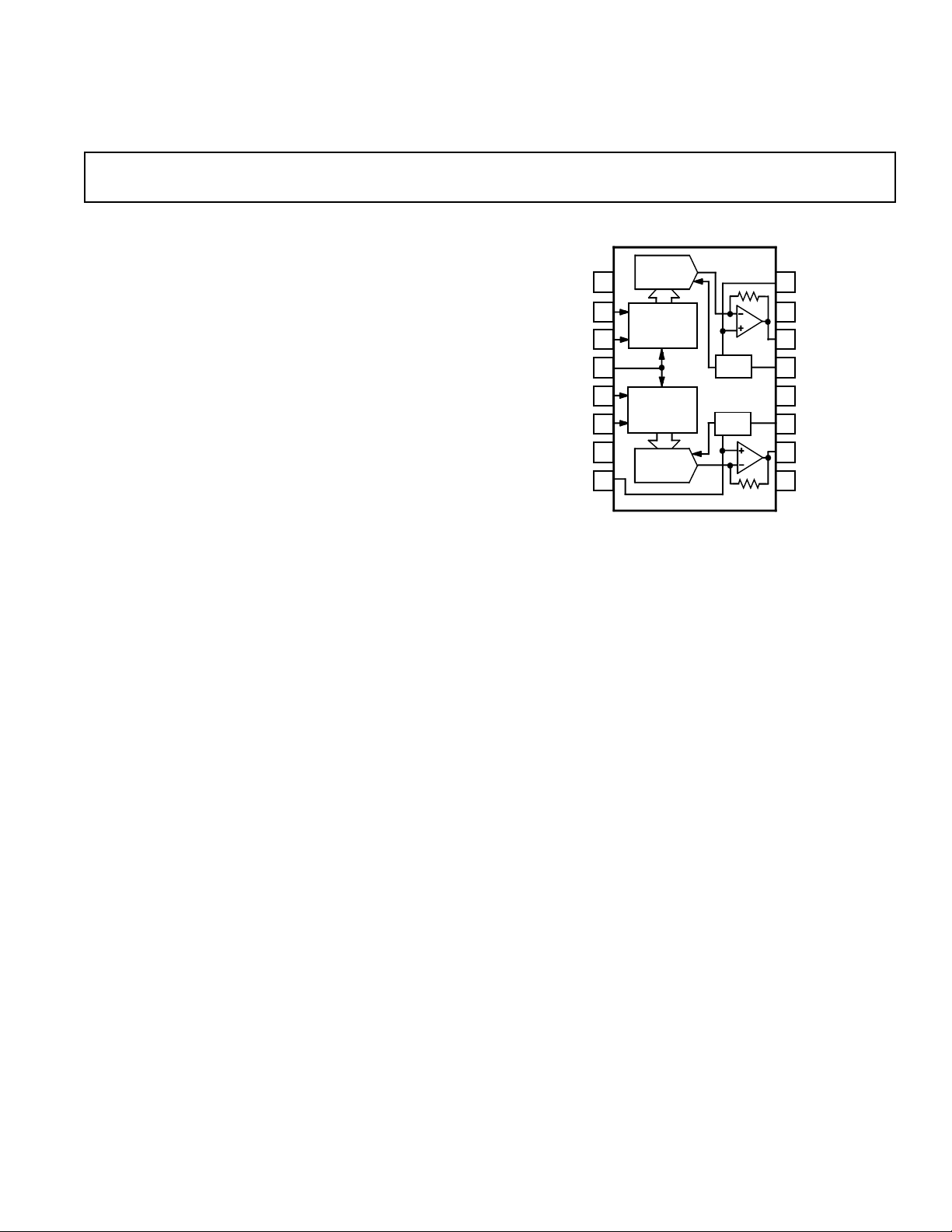
FUNCTIONAL BLOCK DIAGRAM
16-BIT
DAC
16-BIT
SERIAL
REGISTER
16-BIT
SERIAL
REGISTER
16-BIT
DAC
CLK
DGND
VBR
V
DL
DR
LR
1
L
2
LL
3
4
5
6
7
8
The AD1866 operates on +5 V power supplies. The digital
supply, V
, can be separated from the analog supply, VS, for re-
L
duced digital feedthrough. Separate analog and digital ground
pins are also provided. In systems employing a single +5 volt
power supply, V
and VS should be connected together. In bat-
L
tery operated systems, operation will continue even with reduced supply voltage. Typically, the AD1866 dissipates 50 mW.
The AD1866 is packaged in either a 16-pin plastic DIP or a
16-pin plastic SOIC package. Operation is guaranteed over the
temperature range of –35°C to +85°C and over the voltage
supply range of 4.75 V to 5.25 V.
PRODUCT HIGHLIGHTS
1. Single supply operation @ +5 V.
2. 50 mW power dissipation.
3. THD+N is 0.005% (typical).
4. Signal-to-Noise Ratio is 95 dB (typical).
5. 115 dB channel separation (typical).
6. Compatible with all digital filter chips.
7. 16-pin DIP and 16-pin SOIC packages.
8. No deglitcher required.
9. No external adjustments required.
AD1866
V
REF
V
REF
L
V
16
B
V
15
S
L
V
14
O
NRL
13
AGND
12
11
NRR
10
V
R
O
V
9
S
*Protected by U.S. Patent Nos: 3,961,326; 4,141,004; 4,349,811; 4,857,862;
and patents pending.
REV. 0
Information furnished by Analog Devices is believed to be accurate and
reliable. However, no responsibility is assumed by Analog Devices for its
use, nor for any infringements of patents or other rights of third parties
which may result from its use. No license is granted by implication or
otherwise under any patent or patent rights of Analog Devices.
One Technology Way, P.O. Box 9106, Norwood, MA 02062-9106, U.S.A.
Tel: 617/329-4700 Fax: 617/326-8703

AD1866–SPECIFICA TIONS
(TA = +258C and +5 V supplies unless otherwise noted)
Min Typ Max Unit
RESOLUTION 16 Bits
DIGITAL INPUTS V
IH
V
IL
I
, VIH = V
IH
I
, VIL = DGND –10.0 µA
IL
L
2.4 V
0.8 V
1.0 µA
Maximum Clock Input Frequency 13.5 MHz
ACCURACY
Gain Error ±3 % of FSR
Gain Matching ±3 % of FSR
Midscale Error ±30 mV
Midscale Error Matching ±10 mV
Gain Linearity Error ±3dB
DRIFT (0°C to +70°C)
Gain Drift ±100 ppm/°C
Midscale Drift –130 µV/°C
TOTAL HARMONIC DISTORTION + NOISE
0 dB, 990.5 Hz AD1866N 0.005 0.01 %
AD1866R 0.005 0.01 %
–20 dB, 990.5 Hz AD1866N 0.02 %
AD1866R 0.02 %
–60 dB, 990.5 Hz AD1866N 2.0 %
AD1866R 2.0 %
CHANNEL SEPARATION (1 kHz, 0 dB) 108 115 dB
SIGNAL-TO-NOISE RATIO (With A-Weight Filter) 95 dB
D-RANGE (With A-Weight Filter) 90 dB
OUTPUT
Voltage Output Pins (V
OL
, VOR)
Output Range (±3%) ±1V
Output Impedance 0.1 Ω
Load Current ±1mA
Bias Voltage Pins (V
BL
, VBR)
Output Range +2.5 V
Output Impedance 350 Ω
POWER SUPPLY
Specification, V
Operation, V
and V
L
and V
L
S
S
4.75 5 5.25 V
3.5 5.25 V
+I, VL and VS = 5 V 10 14 mA
POWER DISSIPATION 50 70 mW
TEMPERATURE RANGE
Operation –35 85 °C
Storage –60 100 °C
Specifications subject to change without notice.
Specifications in boldface are tested on all production units at final electrical
–2–
REV. 0

T ypical Performance–AD1866
–30
–40
–50
–60
–70
THD+N – dB
–80
–90
–100
FREQUENCY – Hz
–60dB
–20dB
0dB
10500
Figure 1. THD+N vs. Frequency
125
124
123
122
CHANNEL SEPARATION – dB
121
120
2
10
3
10
FREQUENCY – Hz
4
10
Figure 2. Channel Separation vs. Frequency
–30
6
–35°C
4
0°C
2
25°C
0
–2
70°C
–4
GAIN LINEARITY ERROR – dB
–6
125°C
–8
205005500500 15500
–100
–80
INPUT AMPLITUDE – dB
–20–40–60
20
0
Figure 4. Gain Linearity Error vs. Input Amplitude
–30
–40
–50
–60
–70
THD+N – dB
–80
–90
–100
5
10
–75
–50
–25
0
TEMPERATURE – °C
–60dB
–20dB
0dB
100755025
125
Figure 5. THD+N vs. Temperature
80
REV. 0
–40
–50
–60
–70
THD+N – dB
–80
–90
–100
4.4
4.6
SUPPLY VOLTAGE
Figure 3. THD+N vs. Supply Voltage
–60dB
–20dB
0dB
70
60
PSRR – dB
50
40
3
5.45.25.04.8
5.6
10
4
10
FREQUENCY – Hz
5
10
Figure 6. Power Supply Rejection Ratio vs. Frequency
(Supply Modulation Amplitude at 500 mV p-p)
–3–

AD1866
WARNING!
ESD SENSITIVE DEVICE
ABSOLUTE MAXIMUM RATINGS*
VL to DGND . . . . . . . . . . . . . . . . . . . . . . . . . . . . . .0 V to 6 V
V
to AGND . . . . . . . . . . . . . . . . . . . . . . . . . . . . . .0 V to 6 V
S
AGND to DGND . . . . . . . . . . . . . . . . . . . . . . . . . . . . ±0.3 V
Digital Inputs to DGND . . . . . . . . . . . . . . . . . . . –0.3 V to V
*Stresses greater than those listed under “Absolute Maximum Ratings” may cause
permanent damage to the device. This is a stress rating only and functional
operation of the device at these or any other conditions above those indicated in the
operational section of this specification is not implied. Exposure to absolute
maximum rating conditions for extended periods may affect device reliability.
L
Soldering (10 sec) . . . . . . . . . . . . . . . . . . . . . . . . . . . +300°C
CAUTION
ESD (electrostatic discharge) sensitive device. Electrostatic charges as high as 4000 V readily
accumulate on the human body and test equipment and can discharge without detection.
Although the AD1866 features proprietary ESD protection circuitry, permanent damage may
occur on devices subjected to high energy electrostatic discharges. Therefore, proper ESD
precautions are recommended to avoid performance degradation or loss of functionality.
PIN CONFIGURATION
16-BIT
DAC
1
2
16-BIT
SERIAL
REGISTER
3
4
5
16-BIT
SERIAL
REGISTER
6
7
16-BIT
DAC
8
CLK
DGND
VBR
V
L
LL
DL
DR
LR
AD1866
V
REF
V
REF
Pin Mnemonic Description
L
V
16
B
V
15
S
V
L
14
O
NRL
13
AGND
12
11
NRR
10
R
V
O
V
9
S
11V
L
12 LL Left Channel Latch Enable Pin
13 DL Left Channel Data Input Pin
14 CLK Clock Input Pin
15 DR Right Channel Data Input Pin
16 LR Right Channel Latch Enable Pin
17 DGND Digital Common Pin
18V
19V
10 V
R Right Channel Bias Pin
B
S
O
PIN DESIGNATIONS
Digital Supply (+5 V)
Analog Supply (+5 V)
R Right Channel Output Pin
11 NRR Right Channel Noise Reduction Pin
12 AGND Analog Common Pin
13 NRL Left Channel Noise Reduction Pin
14 V
15 V
L Left Channel Output Pin
O
S
Analog Supply (+5 V)
16 VBL Left Channel Bias Pin
ORDERING GUIDE
Temperature Package Package
Model Range Description Option
AD1866N –35°C to +85°C Plastic DIP N-16
AD1866R –35°C to +85°C SOIC R-16
AD1866R-REEL –35°C to +85°C SOIC R-16
–4–
REV. 0
 Loading...