


Complete Dual 18-Bit
a
FEATURES
Dual Serial Input, Voltage Output DACs
No External Components Required
110 dB SNR
0.003% THD+N
Operates at 16 ⴛ Oversampling per Channel
ⴞ5 Volt Operation
Cophased Outputs
116 dB Channel Separation
Pin Compatible with AD1864
DIP or SOIC Packaging
APPLICATIONS
Multichannel Audio Applications
Compact Disc Players
Multivoice Keyboard Instruments
DAT Players and Recorders
Digital Mixing Consoles
Multimedia Workstations
PRODUCT DESCRIPTION
The AD1865 is a complete, dual 18-bit DAC offering excellent
THD+N and SNR while requiring no external components. Two
complete signal channels are included. This results in cophased
voltage or current output signals and eliminates the need for
output demultiplexing circuitry. The monolithic AD1865 chip
includes CMOS logic elements, bipolar and MOS linear elements and laser-trimmed thin-film resistor elements, all fabricated on Analog Devices’ ABCMOS process.
The DACs on the AD1865 chip employ a partially segmented
architecture. The first four MSBs of each DAC are segmented
into 15 elements. The 14 LSBs are produced using standard R-2R
techniques. Segment and R-2R resistors are laser trimmed to provide extremely low total harmonic distortion. This architecture
minimizes errors at major code transitions resulting in low output glitch and eliminating the need for an external deglitcher.
When used in the current output mode, the AD1865 provides
two ±1 mA output signals.
Each channel is equipped with a high performance output amplifier. These amplifiers achieve fast settling and high slew rate,
producing ±3 V signals at load currents up to 8 mA. Each out-
put amplifier is short-circuit protected and can withstand indefinite short circuits to ground.
The AD1865 was designed to balance two sets of opposing requirements, channel separation and DAC matching. High channel separation is the result of careful layout. At the same time,
both channels of the AD1865 have been designed to ensure
matched gain and linearity as well as tracking over time and
temperature. This assures optimum performance when used in
stereo and multi-DAC per channel applications.
*Protected by U.S. Patents Nos.: RE 30,586; 3,961,326; 4,141,004;
4,349,811; 4,855,618; 4,857,862.
REV. 0
Information furnished by Analog Devices is believed to be accurate and
reliable. However, no responsibility is assumed by Analog Devices for its
use, nor for any infringements of patents or other rights of third parties
which may result from its use. No license is granted by implication or
otherwise under any patent or patent rights of Analog Devices.
16 ⴛ FS Audio DAC
AD1865*
FUNCTIONAL BLOCK DIAGRAM
(DIP Package)
–V
S
TRIM
MSB
I
OUT
AGND
SJ
R
V
OUT
+V
DR
LR
CLK
1
2
REFERENCE
3
4
5
6
7
F
8
9
L
10
18-BIT
LATCH
11
12
AD1865
REFERENCE
18-BIT
18-BIT
D/A
D/A
NC = NO CONNECT
LATCH
A versatile digital interface allows the AD1865 to be directly
connected to standard digital filter chips. This interface employs
five signals: Data Left (DL), Data Right (DR), Latch Left (LL),
Latch Right (LR) and Clock (CLK). DL and DR are the serial
input pins for the left and right DAC input registers. Input data
bits are clocked into the input register on the rising edge of
CLK. A low-going latch edge updates the respective DAC output. For systems using only a single latch signal, LL and LR
may be connected together. For systems using only one DATA
signal, DR and DL may be connected together.
The AD1865 operates with ±5 V power supplies. The digital
supply, V
–V
S
, can be separated from the analog supplies, VS and
L
, for reduced digital feedthrough. Separate analog and digital
ground pins are also provided. The AD1865 typically dissipates
only 225 mW, with a maximum power dissipation of 260 mW.
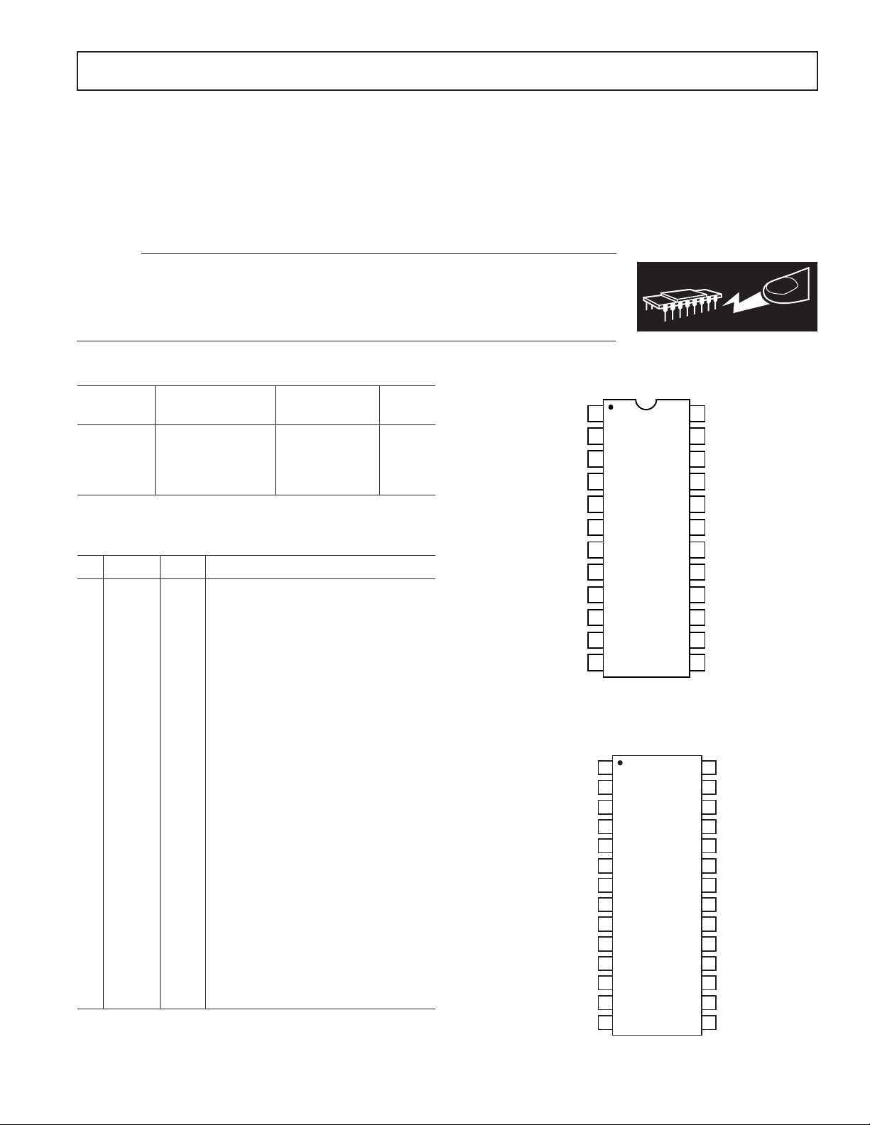
The AD1865 is packaged in both a 24-pin plastic DIP and a
28-pin SOIC package. Operation is guaranteed over the temper-
ature range of –25°C to +70°C and over the voltage supply
range of ±4.75 V to ±5.25 V.
PRODUCT HIGHLIGHTS
11. The AD1865 is a complete dual 18-bit audio DAC.
12. 110 dB signal-to-noise ratio for low noise operation.
13. THD+N is typically 0.003%.
14. Interchannel gain and midscale matching.
15. Output voltages and currents are cophased.
16. Low glitch for improved sound quality.
17. Both channels are 100% tested at 16 × F
18. Low Power—only 225 mW typ, 260 mW max.
19. Five-wire interface for individual DAC control.
10. 24-pin DIP or 28-pin SOIC packages available.
One Technology Way, P.O. Box 9106, Norwood, MA 02062-9106, U.S.A.
Tel: 617/329-4700 Fax: 617/326-8703
18-BIT
24
+V
S
TRIM
23
MSB
22
I
21
OUT
AGND
20
SJ
19
R
18
F
V
17
OUT
16
NC
DL
15
14
LL
13
DGND
.
S

(TA = +25ⴗC, +VL = +VS = +5 V and –VS = –5 V, FS = 705.6 kHz, no MSB adjustment
AD1865–SPECIFICATIONS
or deglitcher)
Parameter Min Typ Max Unit
RESOLUTION 18 Bits
DIGITAL INPUTS V
IH
V
IL
I
, VIH = +V
IH
I
, V
IL
L
= 0.4 V –10 µA
IL
2.0 +V
0.8 V
1.0 µA
L
V
Clock Input Frequency 13.5 MHz
ACCURACY
Gain Error 0.2 1.0 % of FSR
Interchannel Gain Matching 0.3 0.8 % of FSR
Midscale Error 4 mV
Interchannel Midscale Matching 5 mV
Gain Linearity (0 dB to –90 dB) <2 dB
DRIFT (0°C to +70°C)
Gain Drift ±25 ppm of FSR/°C
Midscale Drift ±4 ppm of FSR/°C
TOTAL HARMONIC DISTORTION + NOISE*
0 dB, 990.5 Hz AD1865N, R 0.004 0.006 %
AD1865N-J, R-J 0.003 0.004 %
20 dB, 990.5 Hz AD1865N, R 0.010 0.040 %
AD1865N-J, R-J 0.010 0.020 %
–60 dB, 990.5 Hz AD1865N, R 1.0 4.0 %
AD1865N-J, R-J 1.0 2.0 %
CHANNEL SEPARATION*
0 dB, 990.5 Hz 110 116 dB
SIGNAL-TO-NOISE RATIO* (20 Hz to 30 kHz) 107 110 dB
D-RANGE* (With A-Weight Filter)
–60 dB, 990.5 Hz AD1865N, R 88 100 dB
AD1865N-J, R-J 94 100 dB
OUTPUT
Voltage Output Configuration
Output Range (±1%) ⴞ2.94 ±3.0 ⴞ3.06 V
Output Impedance 0.1 Ω
Load Current ±8mA
Short Circuit Duration Indefinite to Common
Current Output Configuration
Bipolar Output Range (±30%) ±1mA
Output Impedance (±30%) 1.7 kΩ
POWER SUPPLY
and +V
+V
L
–V
S
+I, +V
S
and +VS = +5 V 22 26 mA
L
4.75 5.0 5.25 V
–5.25 –5.0 –4.75 V
–I, –VS = –5 V –23 –26 mA
POWER DISSIPATION, +VL = +VS = +5 V, –VS = –5 V 225 260 mW
TEMPERATURE RANGE
Specification 0 +25 +70 °C
Operation –25 +70 °C
Storage –60 +100 °C
WARMUP TIME 1 min
Specifications shown in boldface are tested on production units at final test without optional MSB adjustment.
*Tested in accordance with EIAJ Test Standard CP-307 with 18-bit data.
Specifications subject to change without notice.
–2–
REV. 0
AD1865
WARNING!
ESD SENSITIVE DEVICE
14
1
2
3
4
5
6
7
8
9
10
11
12
24
23
22
21
20
19
18
17
16
15
13
TOP VIEW
(Not to Scale)
AD1865
+V
S
NC
TRIM
MSB
SJ
DL
LL
DGND
AGND
V
OUT
I
OUT
R
F
–V
S
I
OUT
+V
L
V
OUT
TRIM
MSB
LR
CLK
DR
AGND
SJ
R
F
LEFT
CHANNEL
RIGHT
CHANNEL
NC = NO CONNECT
ABSOLUTE MAXIMUM RATINGS*
VL to DGND . . . . . . . . . . . . . . . . . . . . . . . . . . . . 0 V to 6.0 V
V
to AGND . . . . . . . . . . . . . . . . . . . . . . . . . . . . 0 V to 6.0 V
S
to AGND . . . . . . . . . . . . . . . . . . . . . . . . . . –6.0 V to 0 V
–V
S
AGND to DGND . . . . . . . . . . . . . . . . . . . . . . . . . . . . ±0.3 V
Digital Inputs to DGND . . . . . . . . . . . . . . . . . . . . . –0.3 to V
*Stresses greater than those listed under “Absolute Maximum Ratings” may cause
permanent damage to the device. This is a stress rating only and functional
operation of the device at these or any other conditions above those indicated in the
operational section of this specification is not implied. Exposure to absolute
maximum rating conditions for extended periods may affect device reliability.
L
Short Circuit Protection . . . . . . . . Indefinite Short to Ground
Soldering (10 sec) . . . . . . . . . . . . . . . . . . . . . . . . . . . +300°C
CAUTION
ESD (electrostatic discharge) sensitive device. Electrostatic charges as high as 4000 V readily
accumulate on the human body and test equipment and can discharge without detection.
Although the AD1865 features proprietary ESD protection circuitry, permanent damage may
occur on devices subjected to high energy electrostatic discharges. Therefore, proper ESD
precautions are recommended to avoid performance degradation or loss of functionality.
ORDERING GUIDE
PINOUT
(24-Pin DIP Package)
Temperature Package
Model Range THD+N @ FS Option*
AD1865N –25°C to +70°C 0.006% N-24A
AD1865N-J –25°C to +70°C 0.004% N-24A
AD1865R –25°C to +70°C 0.006% R-28
AD1865R-J –25°C to +70°C 0.004% R-28
*N = Plastic DIP, R = Small Outline IC Package.
DIP SOIC
1122 –V
12 23 TRIM Right Channel Trim Network Connection
13 24 MSB Right Channel Trim Potentiometer
1426 I
15 28 AGND Analog Common Pin
16 11 SJ Right Channel Amplifier Summing Junction
17 12R
18 13V
19 14+V
10 15 DR Right Channel Data Input Pin
11 16 LR Right Channel Latch Pin
12 17 CLK Clock Input Pin
13 18 DGND Digital Common Pin
14 19 LL Left Channel Latch Pin
15 10 DL Left Channel Data Input Pin
16 11, 16, 18 NC No Internal Connection*
17 12 V
18 13 R
19 14 SJ Left Channel Amplifier Summing Junction
20 15 AGND Analog Common Pin
21 17 I
22 19 MSB Left Channel Trim Potentiometer
23 20 TRIM Left Channel Trim Network Connection
24 21 +V
*Pin 16 has no internal connection; –VL from AD1864 DIP socket can be safely
applied.
REV. 0
25, 27
PIN DESIGNATIONS
Negative Analog Supply
S
Wiper Connection
Right Channel Output Current
OUT
Right Channel Feedback Resistor
F
Right Channel Output Voltage
OUT
Positive Digital Supply
L
Left Channel Output Voltage
OUT
Left Channel Feedback Resistor
F
OUT
S
Left Channel Output Current
Wiper Connection
Positive Analog Supply
–3–
(28-Pin SOIC Package)
V
OUT
+V
DR
CLK
DGND
NC
V
OUT
SJ
1
R
F
2
3
4
L
5
LR
6
7
8
LL
9
DL
10
11
12
R
13
F
SJ
14
AD1865
TOP VIEW
(Not to Scale)
NC = NO CONNECT
28
27
26
25
24
23
22
21
20
19
18
17
16
15
AGND
NC
I
OUT
NC
MSB
TRIM
–V
S
+V
S
TRIM
MSB
NC
I
OUT
NC
AGND
AD1865
TOTAL HARMONIC DISTORTION + NOISE
Total harmonic distortion plus noise (THD+N) is defined as
the ratio of the square root of the sum of the squares of the amplitudes of the harmonics and noise to the value of the fundamental input frequency. It is usually expressed in percent.
THD+N is a measure of the magnitude and distribution of linearity error, differential linearity error, quantization error and
noise. The distribution of these errors may be different, depending on the amplitude of the output signal. Therefore, to be most
useful, THD+N should be specified for both large (0 dB) and
small (–20 dB, –60 dB) signal amplitudes. THD+N measurements for the AD1865 are made using the first 19 harmonics
and noise out to 30 kHz.
SIGNAL-TO-NOISE RATIO
The signal-to-noise ratio is defined as the ratio of the amplitude
of the output when a full-scale code is entered to the amplitude
of the output when a midscale code is entered. It is measured
using a standard A-Weight filter. SNR for the AD1865 is measured for noise components out to 30 kHz.
CHANNEL SEPARATION
Channel separation is defined as the ratio of the amplitude of a
full-scale signal appearing on one channel to the amplitude of
that same signal which couples onto the adjacent channel. It is
usually expressed in dB. For the AD1865 channel separation is
measured in accordance with EIAJ Standard CP-307, Section
5.5.
D-RANGE DISTORTION
D-Range distortion is equal to the value of the total harmonic
distortion + noise (THD+N) plus 60 dB when a signal level of
–60 dB below full scale is reproduced. D-Range is tested with a
1 kHz input sine wave. This is measured with a standard A-Weight
filter as specified by EIAJ Standard CP-307.
INTERCHANNEL MIDSCALE MATCHING
The midscale matching specification indicates how closely the
amplitudes of the output signals of the two channels match
when the twos complement input code representing half scale is
loaded into the input register of both channels. It is expressed in
mV and is measured with half-scale output signals.
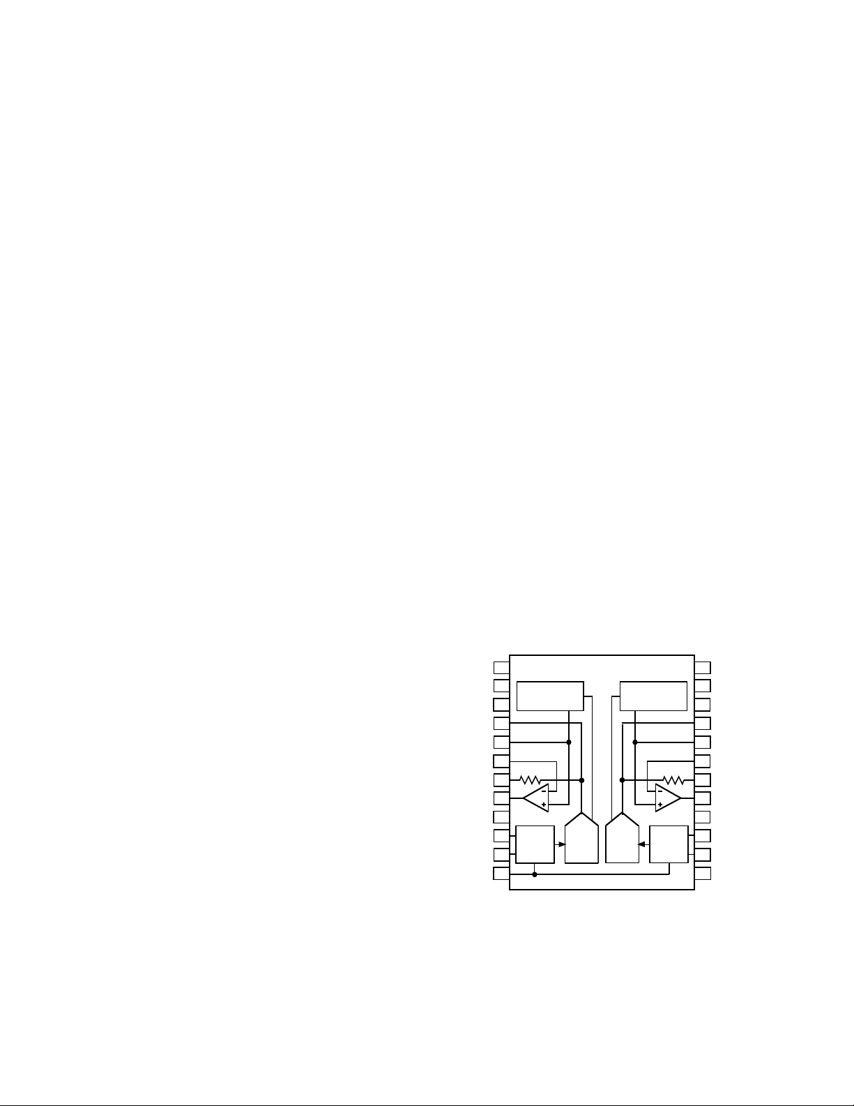
FUNCTIONAL DESCRIPTION
The AD1865 is a complete, monolithic, dual 18-bit audio DAC.
No external components are required for operation. As shown in
the block diagram, each chip contains two voltage references,
two output amplifiers, two 18-bit serial input registers and two
18-bit DACs.
The voltage reference section provides a reference voltage for
each DAC circuit. These voltages are produced by low-noise
bandgap circuits. Buffer amplifiers are also included. This combination of elements produces reference voltages that are unaffected by changes in temperature and age.
The output amplifiers use both MOS and bipolar devices and
incorporate an all NPN output stage. This design technique
produces higher slew rate and lower distortion than previous
techniques. Frequency response is also improved. When combined with the appropriate on-chip feedback resistor, the output
op amps convert the output current to output voltages.
The 18-bit D/A converters use a combination of segmented decoder and R-2R architecture to achieve consistent linearity and
differential linearity. The resistors which form the ladder structure are fabricated with silicon chromium thin film. Laser trimming of these resistors further reduces linearity errors resulting
in low output distortion.
The input registers are fabricated with CMOS logic gates.
These gates allow the achievement of fast switching speeds and
low power consumption, contributing to the low glitch and low
power dissipation of the AD1865.
GAIN ERROR
The gain error specification indicates how closely the output of
a given channel matches the ideal output for given input data. It
is expressed in % of FSR and is measured with a full-scale output signal.
INTERCHANNEL GAIN MATCHING
The gain matching specification indicates how closely the amplitudes of the output signals match when producing identical input data. It is expressed in % of FSR (Full-Scale Range = 6 V
for the AD1865) and is measured with full-scale output signals.
MIDSCALE ERROR
Midscale error is the deviation of the actual analog output of a
given channel from the ideal output (0 V) when the twos
complement input code representing half scale is loaded into the
input register of the DAC. It is expressed in mV and is measured with half-scale output signals.
–V
S
TRIM
MSB
I
OUT
AGND
SJ
R
V
OUT
+V
DR
LR
CLK
1
2
REFERENCE
3
4
5
6
7
F
8
9
L
10
18-BIT
LATCH
11
12
AD1865
REFERENCE
18-BIT
18-BIT
D/A
D/A
NC = NO CONNECT
AD1865 Block Diagram (DIP Package)
18-BIT
LATCH
24
+V
S
TRIM
23
MSB
22
I
21
OUT
AGND
20
SJ
19
R
18
F
V
17
OUT
16
NC
15
DL
14
LL
13
DGND
–4–
REV. 0
100
80
100
120
110
90
0
FREQUENCY – kHz
CHANNEL SEPARATION – dB
4
12 16
8
THD+N – dB
10
8
6
4
2
0
–2
–4
–6
–8
–10
–100 –60 –40 0–80 –20–50 –30 –10
–90
–70
INPUT AMPLITUDE – dB
90
THD+N – dB
80
Typical Performance Data–AD1865
0dB
70
048
FREQUENCY – kHz
12
16
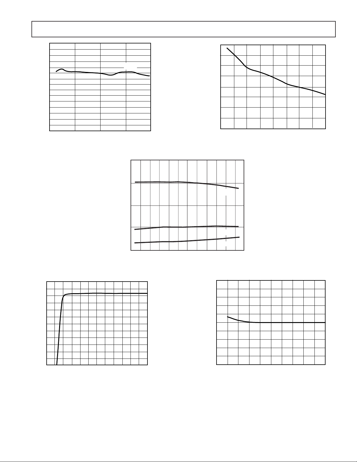
Figure 1. THD+N (dB) vs. Frequency (kHz) Figure 2. Channel Separation (dB) vs. Frequency (kHz)
10
1
–60dB
.1
THD+N – %
.01
.001
–30 –20
–10
0
20 30 40 50 60
10
TEMPERATURE – °C
–20dB
0dB
70 80
90
Figure 3. THD+N (%) vs. Temperature (°C)
100
90
80
70
THD+N – dB
60
50
40
0
500 1000
1500
LOAD RESISTANCE – Ω
Figure 4. THD+N (dB) vs. Load Resistance (Ω)
REV. 0
2000
2500 3000
Figure 5. Gain Linearity (dB) vs. Input Amplitude (dB)
–5–

AD1865–Analog Circuit Consideration
GROUNDING RECOMMENDATIONS
The AD1865 has three ground pins, two labeled AGND and
one labeled DGND. AGND, the analog ground pins, are the
“high quality” ground references for the device. To minimize
distortion and reduce crosstalk between channels, the analog
ground pins should be connected together only at the analog
common point in the system. As shown in Figure 6, the AGND
pins should not be connected at the chip.
–ANALOG
SUPPLY
V
OUT
DIGITAL
SUPPLY
AD1865
–V
S
TRIM
MSB
I
OUT
AGND
SJ
R
F
V
OUT
+V
DR
LR
CLK
+V
TRIM
MSB
I
OUT
AGND
SJ
R
V
OUT
NC
L
DL
LL
DGND
1
2
3
4
5
6
7
8
9
10
11
12
NC = NO CONNECT
24
S
23
22
21
20
19
18
F
17
16
15
14
13
ANALOG
SUPPLY
V
DIGITAL
COMMON
OUT
Figure 6. Recommended Circuit Schematic
The digital ground pin returns ground current from the digital
logic portions of the AD1865 circuitry. This pin should be connected to the digital common pin in the system. Other digital
logic chips should also be referred to that point. The analog and
digital grounds should be connected together at one point in the
system, preferably at the power supply.
POWER SUPPLIES AND DECOUPLING
The AD1865 has three power supply input pins. ±V
provides
S
the supply voltages which operate the analog portions of the
DAC including the voltage references, output amplifiers and
control amplifiers. The ±V
supplies are designed to operate
S
from ±5 V supplies. Each supply should be decoupled to analog
common using a 0.1 µF capacitor in parallel with a 10 µF
capacitor. Good engineering practice suggests that the bypass
capacitors be placed as close as possible to the package pins.
This minimizes the parasitic inductive effects of printed circuit
board traces.
The +V
supply operates the digital portions of the chip includ-
L
ing the input shift registers and the input latching circuitry.
This supply should be bypassed to digital common using a
0.1 µF capacitor in parallel with a 10 µF capacitor. +V
oper-
L
ates with a +5 V supply. In order to assure proper operation of
the AD1865, –V
must be the most negative power supply volt-
S
age at all times.
Though separate positive power supply pins are provided for
the analog and digital portions of the AD1865, it is also possible
to use the AD1865 in systems featuring a single +5 V power
supply. In this case, both the +V
and +VL input pins should be
S
connected to the single +5 V power supply. This feature allows
reduction of the cost and complexity of the system power
supply.
As with most linear circuits, changes in the power supplies will
affect the output of the DAC. Analog Devices recommends that
well regulated power supplies with less than 1% ripple be incorporated into the design of an audio system.
DISTORTION PERFORMANCE AND TESTING
The THD+N figure of an audio DAC represents the amount of
undesirable signal produced during reconstruction and playback
of an audio waveform. The THD+N specification, therefore,
provides a direct method to classify and choose an audio DAC
for a desired level of performance. Figure 1 illustrates the typical THD+N performance of the AD1865 versus frequency. A
load impedance of at least 1.5 kΩ is recommended for best
THD+N performance.
Analog Devices tests and grades all AD1865s on the basis of
THD+N performance. During the distortion test, a high-speed
digital pattern generator transmits digital data to each channel
of the device under test. Eighteen-bit data is transmitted at
705.6 kHz (16 × F
). The test waveform is a 990.5 Hz sine wave
S
with 0 dB, –20 dB and –60 dB amplitudes. A 4096 point FFT
calculates total harmonic distortion + noise, signal-to-noise ratio,
D-Range and channel separation. No deglitchers or MSB trims
are used in the testing of the AD1865.
OPTIONAL MSB ADJUSTMENT
Use of optional adjust circuitry allows residual distortion error
to be eliminated. This distortion is especially important when
low amplitude signals are being reproduced. The MSB adjust
circuitry is shown in Figure 7. The trim potentiometer should
be adjusted to produce the lowest distortion using an input signal with a –60 dB amplitude.
AD1865
+V
–V
200kΩ 100kΩ
470kΩ
10
11
12
1
S
2
TRIM
MSB
3
I
4
OUT
AGND
5
6
SJ
R
7
F
8
V
OUT
+V
9
L
DR
LR
CLK
NC = NO CONNECT
TRIM
MSB
I
OUT
AGND
V
OUT
NC
DL
DGND
24
S
23
22
21
20
SJ
19
R
18
F
17
16
15
14
LL
13
470kΩ 100kΩ
200kΩ
Figure 7. Optional THD+N Adjust Circuitry
REV. 0–6–
Digital Circuit Considerations–AD1865
CURRENT OUTPUT MODE
One or both channels of the AD1865 can be operated in current
output mode. I
can be used to directly drive an external
OUT
current-to-voltage (I-V) converter. The internal feedback resis-
, can still be used in the feedback path of the external I-V
tor, R
F
converter, thus assuring that R
tracks the DAC over time and
F
temperature.
Of course, the AD1865 can also be used in voltage output mode
in order to utilize the onboard I-V converter.
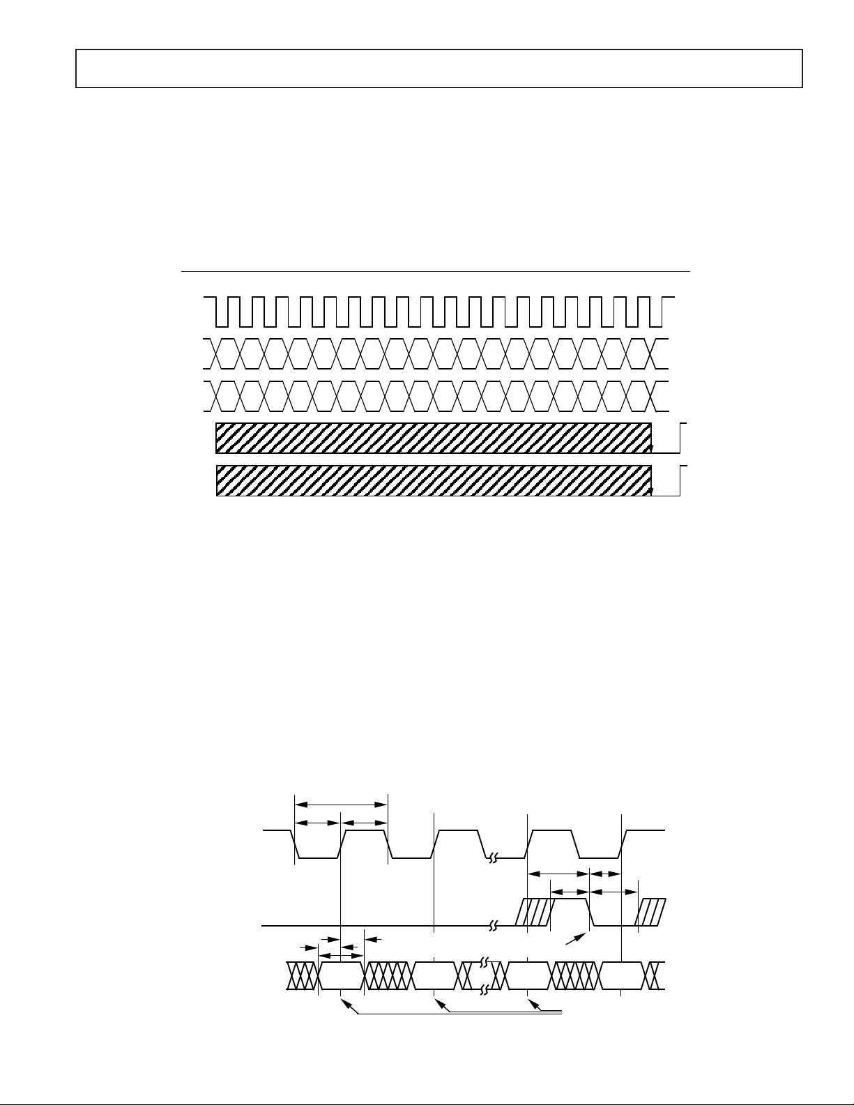
CLK
M
S
DL
B
M
DR
S
B
LL
LR
VOLTAGE OUTPUT MODES
As shown on the block diagram, each channel of the AD1865 is
complete with an I-V converter and a feedback resistor. These
can be connected externally to provide direct voltage output
from one or both AD1865 channels. Figure 6 shows these connections. I
is connected to the Summing Junction, SJ. V
OUT
OUT
is connected to the feedback resistor, RF. This implementation
results in the lowest possible component count and achieves the
specifications shown on the Specifications page while operating
at 16 × F
.
S
L
S
B
L
S
B
Figure 8. AD1865 Control Signals
INPUT DATA
Data is transmitted to the AD1865 in a bit stream composed of
18-bit words with a serial, twos complement, MSB first format.
Data Left (DL) and Data Right (DR) are the serial inputs for
the left and right DACs, respectively. Similarly, Latch Left (LL)
and Latch Right (LR) update the left and right DACs. The falling edge of LL and LR cause the last 18 bits which were clocked
into the Serial Registers to be shifted into the DACs, thereby
updating the DAC outputs. Left and Right channels share the
Clock (CLK) signal. Data is clocked into the input registers on
the rising edge of CLK.
Figure 8 illustrates the general signal requirements for data
transfer for the AD1865.
>74.1ns
>30ns
CLK
>30ns
TIMING
Figure 9 illustrates the specific timing requirements that must
be met in order for the data transfer to be accomplished properly. The input pins of the AD1865 are both TTL and 5 V
CMOS compatible.
The minimum clock rate of the AD1865 is at least 13.5 MHz.
This clock rate allows data transfer rates of 2×, 4×, 8× and
16 × F
(where FS equals 44.1 kHz).
S
>40ns
>15ns
>40ns >40ns
REV. 0
LL/LR
DL/DR
>15ns
>15ns
INTERNAL DAC INPUT REGISTER
UPDATED WITH 18 MOST RECENT BITS
>30ns
MSB
1st BIT
2nd BIT
18th BIT
Figure 9. AD1865 Timing Diagram
–7–
LSB
NEXT
WORD
BITS CLOCKED
TO SHIFT REGISTER

AD1865
SM5813AP/
1
2
3
4
5
6
7
8
VS
9
10
11
12
13
14
–5V ANALOG SUPPLY
+5V ANALOG SUPPLY
AD1865
–V
1
S
TRIM
2
3
MSB
I
OUT
4
AGND
5
6
SJ
7
R
F
8
V
OUT
9
+V
L
10
DR
LR
11
CLK
12
BCKO
WCKO
DOL
DOR
V
VSS2
DG
OW18
OW20
28
27
26
25
24
23
22
DD
21
20
19
18
17
16
15
+5V DIGITAL
C1
SUPPLY
APT
S1
+V
TRIM
MSB
I
OUT
AGND
V
OUT
DGND
NC
24
S
23
22
C2
21
20
SJ
19
R
18
F
17
16
15
DL
14
LL
13
1
2
3
4
–V
S
NE5532
+V
8
S
7
6
5
LEFT
CHANNEL
OUTPUT
RIGHT
CHANNEL
OUTPUT
Figure 10. Complete 8 × FS 18-Bit CD Player
18-BIT CD PLAYER DESIGN
Figure 10 illustrates an 18-bit CD player design incorporating
an AD1865 D/A converter, an NE5532 dual op amp and the
SM5813 digital filter chip manufactured by NPC. In this design, the SM5813 filter transmits left and right digital data to
both channels of the AD1865. The left and right latch signals,
LL and LR, are both provided by the word clock signal
(WCKO) of the digital filter. The digital filter supplies data at
an 8 × F
oversample rate to each channel.
S
The digital data is converted to analog output voltages by the
output amplifiers on the AD1865. Note that no external components are required by the AD1865. Also, no deglitching circuitry is required.
An NE5532 dual op amp is used to provide the output antialias
filters required for adequate image rejection. One 2-pole filter
section is provided for each channel. An additional pole is created from the combination of the internal feedback resistors
) and the external capacitors C1 and C2. For example, the
(R
F
nominal 3 kΩ R
with a 360 pF capacitor for C1 and C2 will
F
place a pole at approximately 147 kHz, effectively eliminating
all high frequency noise components.
Low distortion, superior channel separation, low power consumption and a low parts count are all realized by this simple
design.
–8–
REV. 0
AD1865
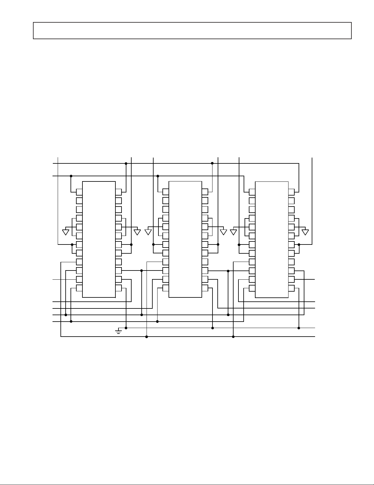
MULTICHANNEL DIGITAL KEYBOARD DESIGN
Figure 11 illustrates how to cascade AD1865’s to add multiple
voices to an electronic musical instrument. In this example, the
data and clock signals are shared between all six DACs. As the
data representing an output for a specific voice is loaded, the appropriate DAC is updated. For example, after the 18-bits representing the next output value for Voice 4 is clocked out on the
data line, then “Voice 4 Load” is pulled low. This produces a
new output for Voice 4. Furthermore, all voices can be returned
to the same output by pulling all six load signals low.
+5V ANALOG
SUPPLY
–5V ANALOG
SUPPLY
ANALOG
COMMON
VOICE 1 LOAD
VOICE 1
OUTPUT
10
11
12
1
2
3
4
5
6
7
8
9
AD1865
–V
S
TRIM
MSB
I
OUT
AGND
SJ
R
F
V
OUT
+V
L
DR
LR
CLK
+V
TRIM
MSB
I
OUT
AGND
SJ
R
V
OUT
NC
DL
LL
DGND
VOICE 2
OUTPUT
24
S
23
22
21
20
19
18
F
17
16
15
14
13
VOICE 3
OUTPUT
10
11
12
1
2
3
4
5
6
7
8
9
AD1865
–V
S
TRIM
MSB
I
OUT
AGND
SJ
R
F
V
OUT
+V
L
DR
LR
CLK
In this application, the advantages of choosing the AD1865 are
clear. Its flexible digital interface allows the clock and data to be
shared among all DACs. This reduces PC board area requirements and also simplifies the actual layout of the board. The low
power requirements of the AD1865 (approximately 225 mW) is
an advantage in a multiple DAC system where any power advantage is multiplied by the number of DACs used. The AD1865
requires no external components, simplifying the design, reducing the total number of components required and enhancing
reliability.
+V
TRIM
MSB
I
OUT
AGND
V
OUT
NC
DGND
VOICE 4
OUTPUT
24
S
23
22
21
20
19
SJ
R
18
F
17
16
15
DL
14
LL
13
VOICE 5
OUTPUT
10
12
1
2
3
4
5
6
7
8
9
11
AD1865
–V
S
TRIM
MSB
I
OUT
AGND
SJ
R
F
V
OUT
+V
L
DR
LR
CLK
+V
TRIM
MSB
I
OUT
AGND
V
OUT
NC
DGND
VOICE 6
OUTPUT
24
S
23
22
21
20
19
SJ
R
18
F
17
16
15
DL
14
LL
13
VOICE 6 LOAD
VOICE 2 LOAD
VOICE 3 LOAD
DATA
CLOCK
REV. 0
VOICE 5 LOAD
VOICE 4 LOAD
DIGITAL COMMON
+5V DIGITAL SUPPLY
Figure 11. Cascaded AD1865s in a Multichannel Keyboard Instrument
–9–

AD1865
ADDITIONAL APPLICATIONS
Figures 12 through 14 show connection diagrams for the AD1865
and standard digital filter chips from Yamaha, NPC and Sony.
Each figure is an example of cophase operation operating at 8 ×
for each channel. The 2-pole Rauch low-pass filters shown in
F
S
Figure 10 can be used with all of the applications shown in this
data sheet.
40
TEST
GND
TEST
TEST
TEST
TEST
CXD1244S
BCKO
DATAL
XIN
GND
V
DD
V
GND
DD
DATAR
LE/
OUT 16/18
LFS
DPOL
SONY/12S
TEST
TEST
TEST
WS
+V
TRIM
MSB
I
OUT
AGND
V
OUT
DGND
NC
DL
24
S
23
22
21
20
19
SJ
R
18
F
17
16
15
14
LL
13
+5V ANALOG
SUPPLY
LPF
LPF
RIGHT
CHANNEL
OUTPUT
LEFT
CHANNEL
OUTPUT
39
38
37
36
35
34
33
32
31
30
29
28
27
26
25
24
23
22
21
–5V ANALOG
SUPPLY
1
2
3
4
5
6
7
8
9
10
11
12
AD1865
–V
S
TRIM
MSB
I
OUT
AGND
SJ
R
F
V
OUT
+V
L
DR
LR
CLK
16.9344
MHz
1
2
3
4
5
6
7
8
9
10
11
12
13
14
15
16
17
18
19
20
1
2
3
4
5
6
7
8
YM3434
SHL
V
DD2
V
DD1
16
SHR
15
16/18
14
ST
13
V
SS
12
BCO
11
WCO
10
DRO
9
DLO
+5V DIGITAL SUPPLY
–5V ANALOG
SUPPLY
1
2
6
8
9
10
11
12
3
4
5
7
AD1865
–V
S
TRIM
MSB
I
OUT
AGND
SJ
R
F
V
OUT
+V
L
DR
LR
CLK
+V
TRIM
MSB
I
OUT
AGND
V
OUT
NC
DGND
24
S
23
22
21
20
19
SJ
R
18
F
17
16
15
DL
14
LL
13
+5V ANALOG
SUPPLY
LPF
LPF
RIGHT
CHANNEL
OUTPUT
LEFT
CHANNEL
OUTPUT
Figure 12. AD1865 with Yamaha YM3434 Digital Filter
–5V ANALOG
SUPPLY
+5V ANALOG
SUPPLY
+5V DIGITAL SUPPLY
Figure 13. AD1865 with Sony CXD1244s Digital Filter
–10–
1
2
3
4
5
6
7
8
V
SM5818
V
BCKO
WDCO
OMOD2
DOR
DOL
OMOD1
SS
AD1865
–V
1
S
2
TRIM
3
MSB
I
4
OUT
AGND
5
16
DD
15
14
13
12
11
10
6
SJ
R
7
F
V
8
OUT
9
+V
L
DR
10
11
LR
12
CLK
9
+V
TRIM
MSB
I
OUT
AGND
R
V
OUT
NC
DL
DGND
24
S
23
22
LPF
RIGHT
CHANNEL
OUTPUT
21
20
19
SJ
18
F
17
LPF
LEFT
CHANNEL
OUTPUT
16
15
14
LL
13
+5V DIGITAL SUPPLY
Figure 14. AD1865 with NPC SM5818AP Digital Filter
REV. 0
OTHER DIGITAL AUDIO COMPONENTS AVAILABLE
FROM ANALOG DEVICES
AD1865
–V
DGND
+V
NC
CLK
DATA
–V
DGND
CLK
DATA
1
S
2
3
L
4
5
6
LE
7
8
L
NC NO CONNECT
1
–V
S
2
3
+V
L
4
NC
5
6
LE
7
8
–V
L
NC NO CONNECT
16-BIT
LATCH
SERIAL
INPUT
REGISTER
CONTROL
LOGIC
AD1856
=
18-BIT
LATCH
SERIAL
INPUT
REGISTER
CONTROL
LOGIC
AD1860
=
16-BIT
DAC
I
OUT
REF
18-BIT
DAC
I
REF
OUT
16
15
14
13
12
11
10
9
16
15
14
13
12
11
10
9
+V
S
TRIM
MSB ADJ
I
OUT
AGND
SJ
R
F
V
OUT
+V
S
TRIM
MSB ADJ
I
OUT
AGND
SJ
R
F
V
OUT
AD1856 16-BIT AUDIO DAC
Complete, No External Components Required
0.0025% THD
Low Cost
16-Pin DIP or SOIC Package
Standard Pinout
AD1860 18-BIT AUDIO DAC
Complete, No External Components Required
0.0025% THD+N
108 dB Signal-to-Noise Ratio
16-Pin DIP or SOIC Package
Standard Pinout
DGND
V
BIAS
–V
–V
TRIM
+V
CLK
DATA
–V
V
LL
DL
CLK
DR
LR
R
1
S
2
S
3
4
L
5
6
LE
L
DIGITAL
OFFSET
7
8
L
1
2
REGISTER
3
4
5
REGISTER
6
7
8
INPUT
&
AD1862
18-BIT
DAC
18-BIT
SERIAL
18-BIT
SERIAL
18-BIT
DAC
VOLTAGE
REFERENCE
20-BIT
DAC
AD1868
V
REF
V
REF
+V
16
S
15
NR
2
14
ADJ
13
NR
1
12
AGND
11
I
OUT
10
R
F
9
DGND
L
V
16
BIAS
V
15
S
V
L
14
OUT
NRL
13
AGND
12
NRR
11
10
V
R
OUT
V
9
S
AD1862 20-BIT AUDIO DAC
119 dB Signal-to-Noise Ratio
0.0016% THD+N
102 dB D-Range Performance
±1 dB Gain Linearity
16-Pin DIP Package
AD1868 +5 V SINGLE SUPPLY DUAL 18-BIT
AUDIO DAC
No External Components Required
0.004% THD+N
92 dB D-Range Performance
±3 dB Gain Linearity
16-Pin DIP or SOIC Package
REV. 0
–11–

AD1865
OUTLINE DIMENSIONS
Dimensions shown in inches and (mm).
24-Pin Plastic DIP
(N-24A) Package
SEATING
PLANE
PIN 1
0.250 (6.35)
0.200 (5.05)
0.125 (3.18)
24
112
1.290 (32.70)
1.150 (29.30)
0.022 (0.558)
0.014 (0.356)
0.070 (1.77)
0.030 (0.77)
13
0.100 (2.54)
BSC
0.580 (14.73)
0.485 (12.32)
0.060 (1.52)
0.015 (0.38)
0.150
(3.81)
0.625 (15.87)
0.600 (15.24)
0.015 (0.381)
0.008 (0.204)
0.195 (4.95)
0.125 (3.18)
C1468–8–8/91
28-Pin SOIC
(R-28) Package
0.708 (18.02)
0.696 (17.67)
28
1
15
14
0.299 (7.6)
0.291 (7.39)
0.414 (10.52)
0.398 (10.10)
0.003 (0.76)
0.02 (0.51)
0.050 (1.27) BSC
0.019 (0.49)
0.014 (0.35)
0.01 (0.254)
0.006 (0.15)
–12–
0.096 (2.44)
0.089 (2.26)
0.013 (0.32)
0.009 (0.23)
0.042 (0.32)
0.009 (0.23)
6°
0°
PRINTED IN U.S.A.
REV. 0
 Loading...