16-Bit 500 kHz
a
FEATURES
16-Bit Resolution
500 kHz Sampling Rate
Differential Linearity Autocalibration
Specified over –558C to +1258C Range
SNR 90 dB @ 100 kHz (min)
THD –88 dB @ 100 kHz (min)
0.0006% FSR DNL (typ)
0.0015% FSR INL (typ)
No Missing Codes
65, 610 V Bipolar Input Ranges
Zero Offset Autocalibration
APPLICATIONS
Medical Imaging
CAT
Magnetic Resonance
Radar
Vibration Analysis
Parametric Measurement Unit (ATE)
Digital Storage Oscilloscopes
Waveform Recorders
Analytical Instruments
Wide Temperature Range Sampling ADC
AD1385
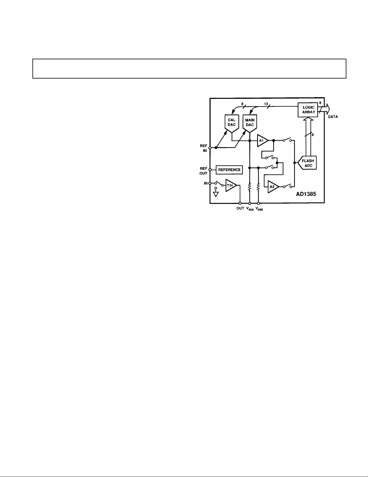
FUNCTIONAL BLOCK DIAGRAM
PRODUCT DESCRIPTION
The AD1385 is a complete 500 kHz, 16-bit, sampling analogto-digital converter contained in a single package. Its differential
linearity autocalibration feature allows this high resolution, high
speed converter to offer outstanding noise and distortion performance, as well as excellent INL and DNL specifications, over
the full military temperature range. Autocalibration effectively
eliminates DNL drift over temperature.
The AD1385 architecture includes a low noise, low distortion
track/hold, a three pass digitally corrected subranging ADC, and
linearity calibration circuitry. A complete linearity calibration
requires only 15 ms. Precision thin-film resistors and a proprietary DAC contribute to the part’s outstanding dynamic and
static performance.
REV. 0
Information furnished by Analog Devices is believed to be accurate and
reliable. However, no responsibility is assumed by Analog Devices for its
use, nor for any infringements of patents or other rights of third parties
which may result from its use. No license is granted by implication or
otherwise under any patent or patent rights of Analog Devices.
The AD1385 uses four power supplies, ± 5 V and ±15 V, and an
external 10 MHz clock. Power dissipation is nominally 2.76 W.
Two user selectable bipolar input ranges, ± 5 V and ±10 V, are
provided. Careful attention to grounding and a single package
make it easy to design PCBs to achieve specified performance.
The AD1385’s pinout is nearly identical to that of the AD1382,
a factory calibrated 16-bit, 500 kHz SADC. Just two additional
connections, to enable and monitor autocalibration, are required.
This commonality provides an easy upgrade path to extend system performance and operating temperature range.
One Technology Way, P.O. Box 9106, Norwood, MA 02062-9106, U.S.A.
Tel: 617/329-4700 Fax: 617/326-8703

AD1385–SPECIFICA TIONS
(TA = +258C, VS = 615 V, VDD = +5 V, VSS = –5 V, 10 MHz External Clock,
unless otherwise noted)
Parameter Min Typ Max Min Typ Max Units
AD1385KD AD1385TD
RESOLUTION 16 16 Bits
ANALOG INPUT
Input Ranges ±5, ±10 ±5, ±10 V
Input Impedance 2.45 2.5 2.55 2.45 2.5 2.55 kΩ
TRANSFER CHARACTERISTICS
(Combined ADC/Track/Hold)
Integral Nonlinearity
Differential Nonlinearity
Drift, T
Drift, T
MIN
4
MIN
Missing Codes, T
Gain Error
Bipolar Zero
Drift, T
MIN
to T
to T
4
to T
MAX
MIN
MAX
MAX
1, 2
, T
to T
1
MIN
MAX
to T
MAX
±0.0015 ±0.0015 % FSR
±0.0006 ±0.0015 ±0.0006 ±0.0015 % FSR
0.3 0.3 ppm/°C
None None
±0.05 ±0.15 ±0.05 ±0.15 % FSR
8 15 8 15 ppm/°C
±0.05 ±0.10 ±0.05 ±0.10 % FSR
5 15 5 15 ppm/°C
PSRR ±0.006 ±0.10 ±0.006 ±0.10 % FSR/V
Noise 70 70 µV rms
MIN
2
to T
MAX
DYNAMIC CHARACTERISTICS
±5 V FSR, VIN = –0.4 dB, T
Sample Rate 500 500 kHz
Signal-to-Noise Ratio
5
f = 5 kHz 90 93 90 93 dB
f = 100 kHz 90 92 90 92 dB
f = 200 kHz 88 91 88 91 dB
Peak Distortion
f = 5 kHz –90 –107 –90 –107 dB
f = 100 kHz –88 –95 –88 –95 dB
f = 200 kHz –82 –88 –82 –88 dB
Total Harmonic Distortion
6
f = 5 kHz –90 –105 –90 –105 dB
f = 100 kHz –88 –95 –88 –95 dB
f = 200 kHz –82 –88 –82 –88 dB
MIN
2
to T
MAX
DYNAMIC CHARACTERISTICS
±10 V FSR, VIN = –0.4 dB, T
Sample Rate 500 500 kHz
Signal-to-Noise Ratio
5
f = 5 kHz 90 95 90 95 dB
f = 100 kHz 90 94 90 94 dB
f = 200 kHz 88 93 88 93 dB
Peak Distortion
f = 5 kHz –90 –108 –90 –108 dB
f = 100 kHz –80 –87 –80 –87 dB
f = 200 kHz –74 –82 –74 –82 dB
Total Harmonic Distortion
6
f = 5 kHz –90 –105 –90 –105 dB
f = 100 kHz –80 –87 –80 –87 dB
f = 200 kHz –74 –82 –74 –82 dB
DIGITAL INPUTS
Input Voltage
V
IL
V
IH
2.25 2.25 V
0.8 0.8 V
Input Current ±200 ±200 µA
Input Capacitance 2 2 pF
Clock
Frequency 2.5–10 2.5–10 MHz
Duty Cycle 40-60 40-60 %
Aperture Delay
7
77ns
DIGITAL OUTPUTS
Output Voltage
@ IOL = 3.2 mA 0.2 0.4 0.2 0.4 V
V
OL
@ IOH = –3.2 mA 2.4 4.5 2.4 4.5 V
V
OH
Output Capacitance 4 4 pF
Leakage, Outputs Disabled ±200 ±200 µA
3
–2–
REV. 0

AD1385
Parameter Min Typ Max Min Typ Max Units
AD1385KD AD1385TD
OUTPUT CODING Complementary Offset Binary or Complementary Twos Complement
INTERNAL REFERENCE
Voltage 9.990 10.010 9.990 10.010 V
Current 2 5 2 5 mA
Drift 5 15 5 15 ppm/°C
TEMPERATURE RANGE, CASE
Specified 0 +70 –55 +125 °C
Storage –65 +150 –65 +150 °C
POWER REQUIREMENTS
Specified Operating Range
±V
+V
–V
S
DD
SS
14.25 15.75 14.25 15.75 V
4.75 5.25 4.75 5.25 V
–5.25 –4.75 –5.25 –4.75 V
Current Drains
+V
–V
+V
–V
S
S
DD
SS
52 80 52 80 mA
48 75 48 75 mA
104 160 104 160 mA
148 200 148 200 mA
Power Dissipation 2.76 4.125 2.76 4.125 Watts
NOTES
1
Integral linearity is inferred from FFTs. Differential linearity is derived from histograms.
2
Performance over temperature is specified at the temperature at which the last calibration was performed.
3
FSR = Full-Scale Range.
4
Adjustable to zero.
5
SNR excludes harmonics 2-9 of the fundamental.
6
THD includes harmonics 2-9 of the fundamental.
7
Aperture delay is the time from the rising edge on the Hold Command Input to the opening of the switch in the Track/Hold.
Specifications subject to change without notice.
1, 2
TIMING SPECIFICATIONS
(TA = –558C to +1258C, VS = 615 V, VDD = +5 V, VSS = –5 V)
Parameter Design Minimum Typ Unit Description
START COMMAND
t
SCS
t
SCH
10 ns Setup Time
10 ns Hold Time
AUTOZERO
t
AZS
t
AZH
DATA VALID
t
DVS
t
DVH
HOLD COMMAND
t
H
t
D
DATA STROBE
t
DS
t
DSD
10 ns Setup Time
20 ns Hold Time
1.5 CP
0.5 CP
13 CP
3
3
3
Setup Time
Hold Time
Hold Time
7 ns Delay Time
2CP
16.5 CP
3
3
Pulse Width
Delay
CALIBRATE PULSE WIDTH 20 ns
CALIBRATION STATUS 15 ms Duration
NOTES
1
Refer to Figures 17, 18 and 24.
2
Design minimums are derived from worst case design analysis and/or simulation results. Typical values are based on characterization data. These specifications are
not guaranteed or tested.
3
The time duration for this parameter varies in direct proportion to the width of the Clock Pulse (CP).
REV. 0
–3–

AD1385
WARNING!
ESD SENSITIVE DEVICE
ABSOLUTE MAXIMUM RATINGS*
+VS to AGND . . . . . . . . . . . . . . . . . . . . . . . . . . . . . . . . . 18 V
–V
to AGND . . . . . . . . . . . . . . . . . . . . . . . . . . . . . . . . –18 V
S
V
to PGND . . . . . . . . . . . . . . . . . . . . . . . . . . . . . . . . . . 7 V
DD
V
to PGND . . . . . . . . . . . . . . . . . . . . . . . . . . . . . . . . . . –7 V
SS
AGND to PGND . . . . . . . . . . . . . . . . . . . . . . . . . . . . ±0.3 V
Analog Inputs . . . . . . . . . . . . . . . . . . . . . . . . . . . . . . . . . .±V
S
Reference Input . . . . . . . . . . . . . . . . . . . . . . . . . .0 V to +11 V
Digital Inputs . . . . . . . . . . . . . . . . . . . . –0.3 V to V
+ 0.3 V
DD
Output Short Circuit Duration
Reference Output . . . . . . . . . . . . . . . . . . . . . . . . . Indefinite
Track/Hold Output . . . . . . . . . . . . . . . . . . . . . . . . . . . 1 sec
Digital Outputs . . . . . . . . . . . . . .1 sec for Any One Output
Case Temperature (Operating) . . . . . . . . . . –55°C to +125°C
Storage Temperature . . . . . . . . . . . . . . . . . . –65°C to +150°C
*Stresses greater than those listed under “Absolute Maximum Ratings” may cause
permanent damage to the device. This is a stress rating only and functional
operation of the device at these or any other conditions above those indicated in
the operational section of this specification is not implied. Exposure to absolute
maximum rating conditions for extended periods may affect device reliability.
ORDERING GUIDE
Temperature
Model Range (Case) Package Option*
AD1385KD 0°C to +70°C DH-48A
AD1385TD –55°C to +125°C DH-48A
AD1385TD/883B –55°C to +125°C DH-48A
*DH-48A = Bottom Brazed Ceramic DIP.
AD1385 PIN CONNECTIONS
The AD1385 is housed in a 48-pin bottom-brazed ceramic
bathtub package. The pinout is as follows:
Pin Function Pin Function
11 CLOCK IN 48 V
(+5 V POWER)
DD2
12 POWER GROUND 47 POWER GROUND
13 B1/B9 (MSB) 46 V
(–5 V POWER)
SS2
14 B2/B10 45 AUTOZERO
15 B3/B11 44 B1 SELECT
16 B4/B12 43 POWER GROUND
17 B5/B13 42 POWER GROUND
18 B6/B14 41
CAL
19 B7/B15 40 GAIN ADJUST
10 B8/B16 (LSB) 39 +10 V REFERENCE OUT
11 V
(+5 V SIGNAL) 38 –VS1 (–15 V)
DD1
12 POWER GROUND 37 SIGNAL GROUND
13 V
(–5 V SIGNAL) 36 +VS1 (+15 V)
SS1
14 SIGNAL GROUND 35 SIGNAL GROUND
15 DATA STROBE 34 DNC
16 HI/LO BYTE SELECT 33 DNC
17
OE DATA ENABLE 32 +10 V REFERENCE IN
18 START CONVERT 31 V
B
IN
19 HOLD COMMAND OUT 30 VIN A
20 SIGNAL GROUND 29 OFFSET ADJUST
21 +V
(+15 V) 28 CAL STATUS
S2
22 HOLD COMMAND IN 27 TRACK/HOLD OU TPUT
23 –VS2 (–15 V) 26 SIGNAL GROUND
24 POWER GROUND 25 TRACK/HOLD INPUT
DNC = DO NOT CONNECT.
CAUTION
ESD (electrostatic discharge) sensitive device. Electrostatic charges as high as 4000 V readily
accumulate on the human body and test equipment and can discharge without detection.
Although the AD1385 features proprietary ESD protection circuitry, permanent damage may
occur on devices subjected to high energy electrostatic discharges. Therefore, proper ESD
precautions are recommended to avoid performance degradation or loss of functionality.
–4–
REV. 0

AD1385
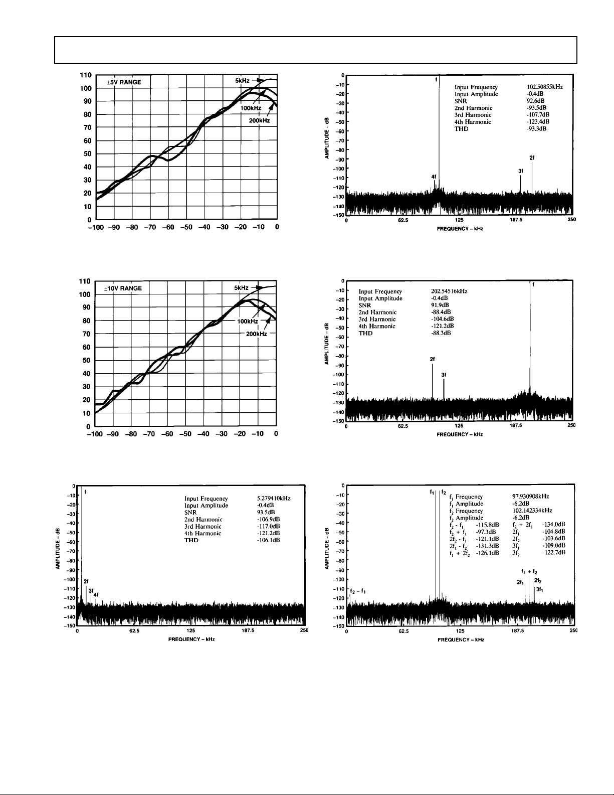
Figure 1. Spurious-Free Range vs. Input Amplitude,
±
5 V Range, 2048-Point FFT, 500 kHz Sample Rate
Figure 2. Spurious-Free Range vs. Input Amplitude,
±
10 V Range, 2048-Point FFT, 500 kHz Sample Rate
Figure 4. Full-Scale Sine Wave Power Spectral Density,
±
5 V Range, 16384-Point FFT, 500 kHz Sample Rate
Figure 5. Full-Scale Sine Wave Power Spectral Density,
±
5 V Range, 16384-Point FFT, 500 kHz Sample Rate
Figure 3. Full-Scale Sine Wave Power Spectral Density,
±
5 V Range, 16384-Point FFT, 500 kHz Sample Rate
REV. 0
Figure 6. 100 kHz Intermodulation Performance, ±5 V
Range, 16384-Point FFT, 500 kHz Sample Rate
–5–

AD1385
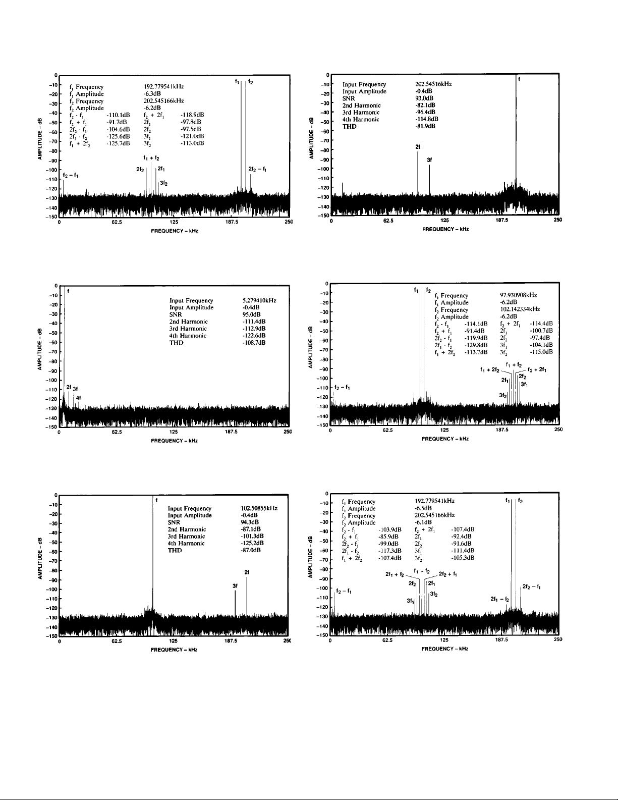
Figure 7. 200 kHz Intermodulation Performance, ±5 V
Range, 16384-Point FFT, 500 kHz Sample Rate
Figure 8. Full-Scale Sine Wave Power Spectral Density,
±
10 V Range, 16384-Point FFT, 500 kHz Sample Rate
Figure 10. Full-Scale Sine Wave Power Spectral Density,
±
10 V Range, 16384-Point FFT, 500 kHz Sample Rate
Figure 11. 100 kHz Intermodulation Performance, ±10 V
Range, 16384-Point FFT, 500 kHz Sample Rate
Figure 9. Full-Scale Sine Wave Power Spectral Density,
±
10 V Range, 16384-Point FFT, 500 kHz Sample Rate
Figure 12. 200 kHz Intermodulation Performance, ±10 V
Range, 16384-Point FFT, 500 kHz Sample Rate
–6–
REV. 0
 Loading...