

AMD MACH211SP-12JI, MACH211SP-12JC, MACH211SP-10VC, MACH211SP-10JI, MACH211SP-10JC Datasheet
...
FINAL
Publication# 20405 Rev: B Amendment/0
Issue Date: February 1996
COM’L: -7.5/10/12/15/20 IND: -10/12/14/18/24
MACH211SP-7/10/12/15/20
High-Density EE CMOS Programmable Logic
DISTINCTIVE CHARACTERISTICS
■
JTAG-Compatible, 5-V in-system programming
■
44 Pins
■
64 Macrocells
■
7.5 ns t
PD
Commercial
10 ns t
PD
Industrial
■
133 MHz f
CNT
■
34 Bus-Friendly™ Inputs and I/Os
■
Peripheral Component Interconnect (PCI)
compliant (-7/-10)
■
Programmable power-down mode
■
32 Outputs
■
64 Flip-flops; 2 clock choices
■
4 “PAL26V16” blocks with buried macrocells
■
Improved routing over the MACH210
IN-SYSTEM PROGRAMMING
In-system programming allows the MACH211SP to be
programmed while soldered onto a system board. Programming the MACH211SP in-system yields numerous benefits at all stages of development: prototyping,
manufacturing, and in the field. Since insertion into a
programmer isn’t needed, multiple handling steps and
the resulting bent leads are eliminated. The design can
be modified in-system for design changes and debugging while prototyping, programming boards in production, and field upgrades.
The MACH211SP offers advantages not available in
other CPLD architectures with in-system programming.
MACH devices have extensive routing resources for
pin-out retention; design changes resulting in pin-out
changes for other CPLDs cancel the advantages of
in-system programming. The MACH211SP can be employed in any JTAG (IEEE 1149.1) compliant chain.
GENERAL DESCRIPTION
The MACH211SP is a member of AMD’s EE CMOS
Performance Plus MACH
2 device family. This device
has approximately six times the logic macrocell capability of the popular PAL22V10 without loss of speed.
The MACH211SP consists of four PAL blocks interconnected by a programmable switch matrix. The four
PAL blocks are essentially “PAL26V16” structures complete with product-term arrays and programmable
macrocells, which can be programmed as high speed
or low power, and buried macrocells. The switch matrix
connects the PAL blocks to each other and to all input
pins, providing a high degree of connectivity between
the fully-connected PAL blocks. This allows designs to
be placed and routed efficiently.
The MACH211SP has two kinds of macrocell: output
and buried. The MACH211SP output macrocell provides registered, latched, or combinatorial outputs with
programmable polarity. If a registered configuration is
chosen, the register can be configured as D-type or
T-type to help reduce the number of product terms. The
register type decision can be made by the designer or
by the software. All output macrocells can be connected to an I/O cell. If a buried macrocell is desired,
the internal feedback path from the macrocell can be
used, which frees up the I/O pin for use as an input.
The MACH211SP has dedicated buried macrocells
which, in addition to the capabilities of the output
macrocell, also provide input registers or latches for
use in synchronizing signals and reducing setup time
requirements.
The MACH211SP is an enhanced version of the
MACH211, adding the JTAG-compatible in-system programming feature.

2 MACH211SP-7/10/12/15/20
BLOCK DIAGRAM
20405B-1
Switch Matrix
I/O Cells
Macrocells
I/O
0
–I/O
7
Macrocells
8
8
8
2
CLK
0/I0
CLK1/I
1
52 x 68
AND Logic Array
and
Logic Allocator
26
2
8
2
OE
I/O Cells
Macrocells
I/O
8
–I/O
15
Macrocells
8
8
8
52 x 68
AND Logic Array
and
Logic Allocator
26
8
OE
I/O Cells
Macrocells
I/O
24
–I/O
31
Macrocells
8
8
8
52 x 68
AND Logic Array
and
Logic Allocator
26
8
OE
I/O Cells
Macrocells
I/O
16
–I/O
23
Macrocells
8
8
8
52 x 68
AND Logic Array
and
Logic Allocator
26
8
OE
MACH211SP-7/10/12/15/20 3
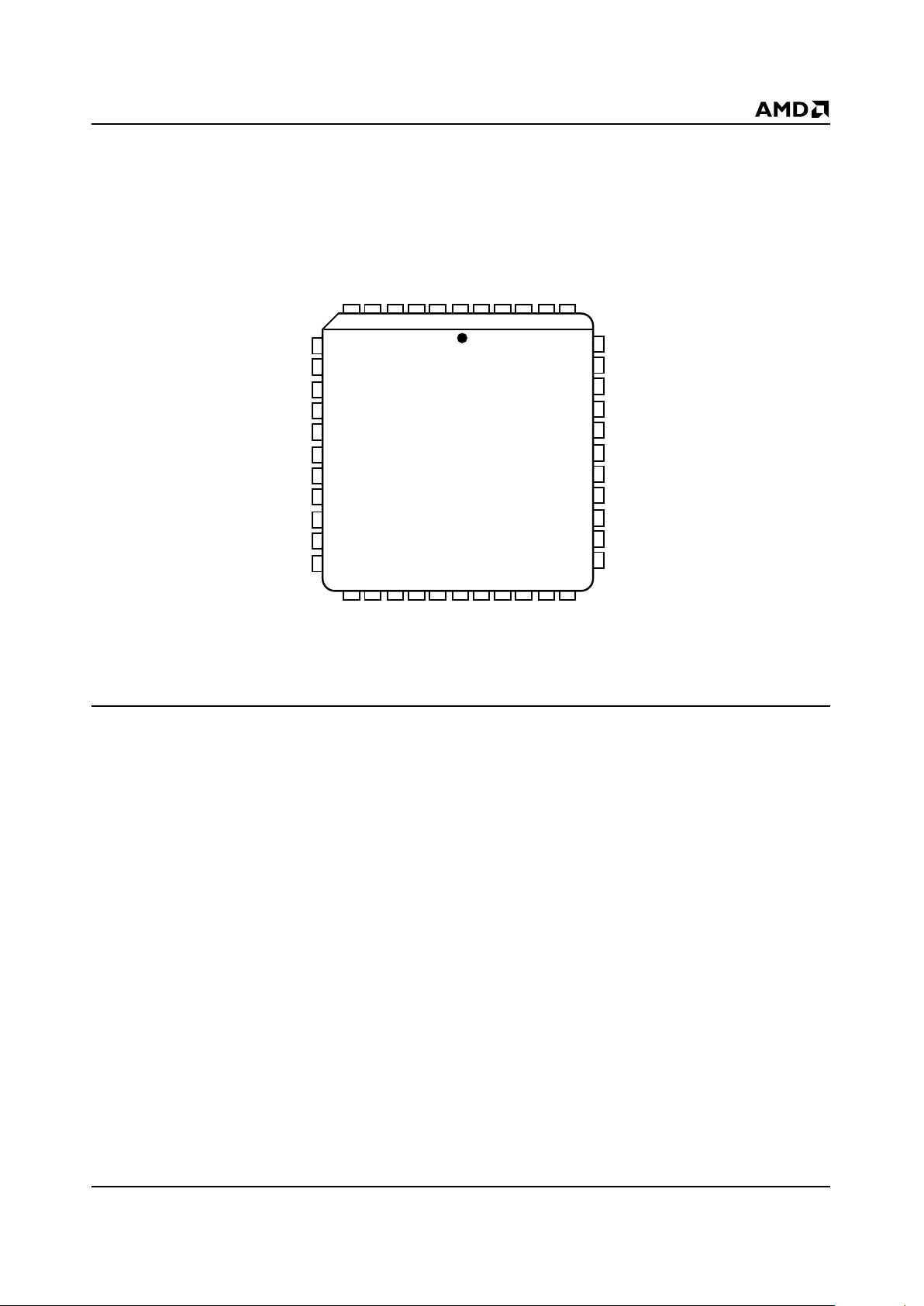
CONNECTION DIAGRAM MACH211SP
T op View
44-Pin PLCC
PIN DESIGNATIONS
CLK/I = Clock or Input
GND = Ground
I = Input
I/O = Input/Output
V
CC
= Supply V oltage
TDI = Test Data In
TCK = Test Clock
TMS = Test Mode Select
TDO = Test Data Out
1
44
43
42
5
4
3
2
641
40
7
8
9
10
11
12
13
14
15
16
17
23
24
25
26
19
20
21
22
18 27
28
39
38
37
36
35
34
33
32
31
30
29
I/O5
I/O6
I/O7
TDI
CLK0/I0
GND
TCK
I/O8
I/O9
I/O10
I/O11
I/O27
I/O26
I/O25
I/O24
TDO
GND
CLK1/I1
TMS
I/O23
I/O22
I/O21
I/O12
I/O13
I/O14
I/O15
VCC
GND
I/O16
I/O17
I/O18
I/O19
I/O20
I/O4
I/O3
I/O2
I/O1
I/O0
GND
VCC
I/O31
I/O30
I/O29
I/O28
20405B-2

4 MACH211SP-7/10/12/15/20
CONNECTION DIAGRAM MACH211SP
T op View
44-Pin TQFP
PIN DESIGNATIONS
CLK/I = Clock or Input
GND = Ground
I = Input
I/O = Input/Output
V
CC
= Supply Voltage
TDI = Test Data In
TCK = Test Clock
TMS = Test Mode Select
TDO = Test Data Out
I/O12
I/O13
I/O14
I/O15
VCC
GND
I/O16
I/O17
I/O18
I/O19
I/O20
I/O4
I/O3
I/O2
I/O1
I/O0
GND
VCC
I/O31
I/O30
I/O29
I/O28
I/O27
I/O26
I/O25
I/O24
TDO
GND
CLK1/I1
TMS
I/O23
I/O22
I/O21
I/O5
I/O6
I/O7
TDI
CLK0/I0
GND
TCK
I/O8
I/O9
I/O10
I/O11
1
2
3
4
5
6
7
8
9
10
11
33
32
31
30
29
28
27
26
25
24
23
4443424140
39
38
373635
34
1213141516
17
18
192021
22
20405B-3
MACH211SP-7/10/12/15/20 (Com’l) 5
ORDERING INFORMATION
Commercial Products
AMD programmable logic products for commercial applications are available with several ordering options. The order number
(Valid Combination) is formed by a combination of:
Valid Combinations
The Valid Combinations table lists configurations planned to
be supported in volume for this device. Consult the local AMD
sales office to confirm availability of specific valid combinations and to check on newly released combinations.
F AMIL Y TYPE
MACH = Macro Array CMOS High-Speed
MACH 211 SP -7 J C
DEVICE NUMBER
211 = 64 Macrocells, 44 Pins,
Power-Down mode,
Bus-Friendly Inputs and I/Os
PRODUCT DESIGNATION
SP = In-system Programmable
OPTIONAL PROCESSING
Blank = Standard Processing
OPERATING CONDITIONS
C = Commercial (0°C to +70°C)
P ACKA GE TYPE
J = 44-Pin Plastic Leaded Chip
Carrier (PL 044)
V = 44-Pin Thin Quad Flat Pack
(PQT044)
SPEED
-7 = 7.5 ns t
PD
-10 = 10 ns t
PD
-12 = 12 ns t
PD
-15 = 15 ns t
PD
-20 = 20 ns t
PD
Valid Combinations
MACH211SP-7
JC, VC
MACH211SP-10
MACH211SP-12
MACH211SP-15
MACH211SP-20
6 MACH211SP-10/12/14/18/24 (Ind)
ORDERING INFORMATION
Industrial Products
AMD programmable logic products for industrial applications are av ailab le with se v er al ordering options. The order number (Valid
Combination) is formed by a combination of:
Valid Combinations
The Valid Combinations table lists configurations planned to
be supported in volume for this device. Consult the local AMD
sales office to confirm availability of specific valid combinations and to check on newly released combinations.
DEVICE NUMBER
211 = 64 Macrocells, 44 Pins,
Power-Down mode,
Bus-Friendly Inputs and I/Os
PRODUCT DESIGNATION
SP = In-system Programmable
F AMIL Y TYPE
MACH = Macro Array CMOS High-Speed
MACH 211 SP -10 J I
OPTIONAL PROCESSING
Blank = Standard Processing
OPERATING CONDITIONS
I = Industrial (–40
°C to +85°C)
P ACKA GE TYPE
J = 44-Pin Plastic Leaded Chip
Carrier (PL 044)
SPEED
-10 = 10 ns t
PD
-12 = 12 ns t
PD
-14 = 14.5 ns t
PD
-18 = 18 ns t
PD
-24 = 24 ns t
PD
Valid Combinations
MACH211SP-10
JI
MACH211SP-12
MACH211SP-14
MACH211SP-18
MACH211SP-24
MACH211SP-7/10/12/15/20 7
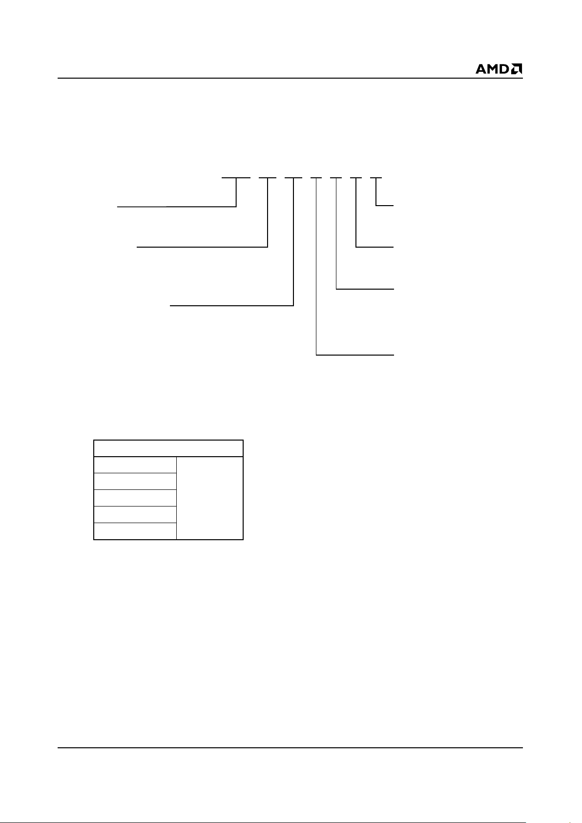
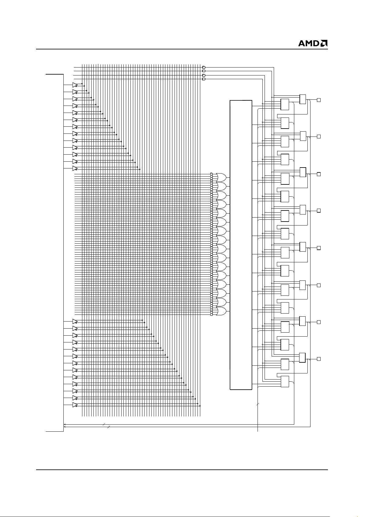
FUNCTIONAL DESCRIPTION
The MACH211SP consists of four PAL blocks connected by a switch matrix. There are 32 I/O pins feeding
the switch matrix. These signals are distributed to the
four PAL blocks for efficient design implementation.
There are two clock pins that can also be used as dedicated inputs.
The PAL Blocks
Each P AL b lock in the MA CH211SP (Figure 1) contains
a 64-product-term logic array , a logic allocator, 8 output
macrocells, 8 buried macrocells, and 8 I/O cells. The
switch matrix feeds each PAL block with 26 inputs. This
makes the PAL block look effectively like an independent “PAL26V16” with 8 buried macrocells.
In addition to the logic product terms, two output enable
product terms, an asynchronous reset product term,
and an asynchronous preset product term are provided. One of the two output enable product terms can
be chosen within each I/O cell in the PAL block. All
flip-flops within the PAL block are initialized together.
The Switch Matrix
The MACH211SP switch matrix is f ed by the inputs and
feedback signals from the PAL blocks. Each PAL block
provides 16 internal feedback signals and 8 I/O feedback signals. The switch matrix distributes these signals back to the PAL blocks in an efficient manner that
also provides for high performance. The design software automatically configures the switch matrix when
fitting a design into the device.
The Product-term Array
The MACH211SP product-term array consists of 64
product terms for logic use, and 4 special-purpose
product terms. Two of the special-purpose product
terms provide programmable output enable; one provides asynchronous reset, and one provides asynchronous preset.
The Logic Allocator
The logic allocator in the MACH211SP takes the 64
logic product terms and allocates them to the 16
macrocells as needed. Each macrocell can be driven
by up to 16 product terms. The design software automatically configures the logic allocator when fitting the
design into the device.
T ab le 1 illustrates which product term clusters are available to each macrocell within a PAL block. Refer to
Figure 1 for cluster and macrocell numbers.
The Macrocell
The MACH211SP has two types of macrocell: output
and buried. The output macrocells can be configured
as either registered, latched, or combinatorial, with programmable polarity. The macrocell provides internal
feedback whether configured with or without the
flip-flop. The registers can be configured as D-type or
T-type, allowing for product-term optimization.
The flip-flops can individually select one of two clock/
gate pins, which are also available as data inputs. The
registers are clocked on the LOW-to-HIGH transition of
the clock signal. The latch holds its data when the gate
input is HIGH, and is transparent when the gate input
is LOW. The flip-flops can also be asynchronously initialized with the common asynchronous reset and preset product terms.
The buried macrocells are the same as the output
macrocells if they are used for generating logic. In that
case, the only thing that distinguishes them from the
output macrocells is the fact that there is no I/O cell
connection, and the signal is only used internally. The
buried macrocell can also be configured as an input
register or latch.
The I/O Cell
The I/O cell in the MACH211SP consists of a
three-state output buffer. The three-state buffer can be
configured in one of three ways: always enabled, always disabled, or controlled by a product term. If product term control is chosen, one of two product terms
may be used to provide the control. The two product
terms that are available are common to all I/O cells in a
PAL block.
Table 1. Logic Allocation
Macrocell
Available ClustersOutput Buried
M
0
C
0
, C
1
, C
2
M
1
C
0
, C
1
, C
2
, C
3
M
2
C
1
,
C
2
,
C
3
,
C
4
M
3
C
2
,
C
3
,
C
4
,
C
5
M
4
C3, C4, C5, C
6
M
5
C4, C5, C6, C
7
M
6
C5, C6, C7, C
8
M
7
C6, C7, C8, C
9
M
8
C7, C8, C9, C
10
M
9
C8, C9, C10, C
11
M
10
C9, C10, C11, C
12
M
11
C10, C11, C12, C
13
M
12
C11, C12, C13, C
14
M
13
C12, C13, C14, C
15
M
14
C13, C14, C
15
M
15
C14, C
15

8 MACH211SP-7/10/12/15/20
These choices make it possible to use the macrocell as
an output, an input, a bidirectional pin, or a three-state
output for use in driving a bus.
Power-Down Mode
The MACH211SP features a progr ammab le low-po w er
mode in which individual signal paths can be programmed as low power. These low-power speed paths
will be slightly slower than the non-low-power paths.
This feature allows speed critical paths to run at maximum frequency while the rest of the paths operate in
the low-power mode, resulting in power savings of up
to 75%. If all signals in a PAL block are low-pow er , then
total power is reduced further.
In-System Programming
Programming is the process where MACH devices are
loaded with a pattern defined in a JEDEC file obtained
from MACHXL software or third-party software. Programming is accomplished through four JTAG pins:
Test Mode Select (TMS), Test Clock (TCK), Test Data
In (TDI), and Test Data Out (TDO). The MACH211SP
can be employed in any JTAG (IEEE 1149.1) compliant chain. While the MACH211SP is fully JTAG compatible, it supports the BYPASS instruction, not the
EXTEST and SAMPLE/PRELOAD instructions. The
MACH211SP can be programmed across the commercial temperature range. Programming the MACH device after it has been placed on a circuit board is easily
accomplished. Programming is initiated by placing the
device into programming mode, using the MACHPRO
programming software provided by AMD. The device is
bulk erased and the JEDEC file is then loaded. After
the data is transferred into the device, the PROGRAM
instruction is loaded. Further programming details can
be found in application note, “Advanced In-circuit
Programming Guidelines.”
On-Board Programming Options
Since the MACHPRO software performs these steps
automatically, the following programming options are
published for reference.
The configuration file, which is also known as the chain
file, defines the MACH de vice JTAG chain. The file contains the information concerning which JEDEC file is to
be placed into which device, the state which the outputs should be placed, and whether the security fuses
should be programmed. The configuration file is discussed in detail in the MACHPRO software manual.
The MACH211SP devices tristate the outputs during
programming. They hav e one security bit which inhibits
program and verify. This allows the user to protect proprietary patterns and designs.
Program verification of a MACH device involves reading back the programmed pattern and comparing it with
the original JEDEC file. The AMD method of program
verification performed on the MACH devices permits
the verification of one device at a time.
Accidental Programming or Erasure
Protection
It is virtually impossible to program or erase a MACH
device inadvertently. The following conditions must be
met before programming actually takes place:
■ The device must be in the password-protected
program mode
■ The programming or bulk erase instruction must be
in the instruction register
If the above conditions are not met, the programming
circuitry cannot be activated.
To ensure that the AMD ten year device data retention
guarantee applies, 100 program/erase cycle limit
should not be exceeded.
Bus-Friendly Inputs and I/Os
The MACH211SP inputs and I/Os include two inv erters
in series which loop back to the input. This double
inversion reinforces the state of the input and pulls the
voltage away from the input threshold voltage. For an
illustration of this configuration, please turn to the
Input/Output Equivalent Schematics section.
PCI Compliance
The MACH211SP-7/10 is fully compliant with the
PCI
Local Bus Specification
published by the PCI Special
Interest Group. The MACH211SP-7/10’s predictable
timing ensures compliance with the PCI AC specifications independent of the design. On the other hand, in
CPLD and FPGA architectures without predictable timing, PCI compliance is dependent upon routing and
product term distribution.
MACH211SP-7/10/12/15/20 9
0 4 8 12 16 20 24 28 40324336
0 4 8 12 16 20 24 28 40324336
I/O
Cell
I/O
I/O
I/O
I/O
I/O
I/O
I/O
I/O
Switch
Matrix
Output Enable
Output Enable
Asynchronous Reset
Asynchronous Preset
16
I/O
Cell
I/O
Cell
I/O
Cell
I/O
Cell
I/O
Cell
I/O
Cell
I/O
Cell
Output
Macro
Cell
Output
Macro
Cell
Output
Macro
Cell
Output
Macro
Cell
Output
Macro
Cell
Output
Macro
Cell
Output
Macro
Cell
Output
Macro
Cell
8
Buried
Macro
Cell
Buried
Macro
Cell
Buried
Macro
Cell
Buried
Macro
Cell
Buried
Macro
Cell
Buried
Macro
Cell
Buried
Macro
Cell
Buried
Macro
Cell
47
51
47
51
CLK
2
0
Logic Allocator
63
C
0
C
1
C
2
C
3
C
4
C
5
C
6
C
7
C
8
C
9
C
10
C
11
C
12
C
13
C
14
C
15
M
3
M
6
M
5
M
4
M
2
M
1
M
0
M
9
M
8
M
7
M
10
M
11
M
12
M
13
M
14
M
15
20405B-4
Figure 1. MACH211SP PAL Block
10 MACH211SP-7/10 (Com’l)
ABSOLUTE MAXIMUM RATINGS
Storage Temperature . . . . . . . . . . . . –65°C to +150°C
Ambient Temperature
with Power Applied. . . . . . . . . . . . . . –55°C to +125°C
Supply V oltage with
Respect to Ground. . . . . . . . . . . . . . .–0.5 V to +7.0 V
DC Input Voltage . . . . . . . . . . . .–0.5 V to VCC + 0.5 V
DC Output or
I/O Pin Voltage . . . . . . . . . . . . . .–0.5 V to V
CC
+ 0.5 V
Static Discharge Voltage . . . . . . . . . . . . . . . . . 2001 V
Latchup Current (TA = 0°C to 70°C). . . . . . . . 200 mA
Stresses above those listed under Absolute Maximum
Ratings may cause permanent device failure. Functionality at
or above these limits is not implied. Exposure to Absolute
Maximum Ratings for extended periods may affect device
reliability. Programming conditions may differ.
OPERATING RANGES
Commercial (C) Devices
Ambient Temperature (TA)
Operating in Free Air. . . . . . . . . . . . . . . .0°C to +70°C
Supply V oltage (VCC)
with Respect to Ground . . . . . . . . +4.75 V to +5.25 V
Operating ranges define those limits between which the
functionality of the device is guaranteed.
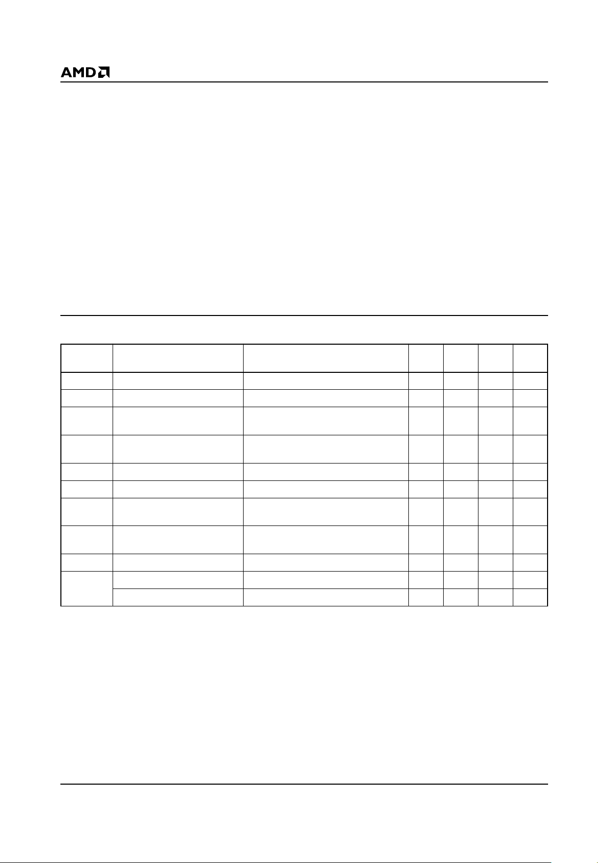
DC CHARACTERISTICS over COMMERCIAL operating ranges unless otherwise specified
Notes:
1. These are absolute values with respect to device ground and all overshoots due to system and/or tester noise are included.
2. I/O pin leakage is the worst case of I
IL
and I
OZL
(or IIH and I
OZH
).
3. Not more than one output should be shorted at a time. Duration of the short-circuit should not exceed one second.
V
OUT
= 0.5 V has been chosen to avoid test problems caused by tester ground degradation.
4. This parameter is measured in low-power mode with a 16-bit up/down counter pattern. This pattern is programmed in each
PAL block and is capable of being loaded, enabled and reset.
5. This parameter is not 100% tested, but is evaluated at initial characterization and at any time the design is modified where
capacitance may be affected.
Parameter
Symbol Parameter Description Test Conditions Min Typ Max Unit
V
OH
Output HIGH Voltage IOH = –3.2 mA, VCC = Min, VIN = VIH or VIL2.4 V
V
OL
Output LOW Voltage IOL = 16 mA, VCC = Min, VIN = VIH or V
IL
0.5 V
V
IH
Input HIGH Voltage
Guaranteed Input Logical HIGH
Voltage for all Inputs (Note 1)
2.0 V
V
IL
Input LOW Voltage
Guaranteed Input Logical LOW
Voltage for all Inputs (Note 1)
0.8 V
I
IH
Input HIGH Current VIN = 5.25 V, VCC = Max (Note 2) 10 µA
I
IL
Input LOW Current VIN = 0 V, V
CC
= Max (Note 2) –10 µA
I
OZH
Off-State Output Leakage
Current HIGH
V
OUT
= 5.25 V, V
CC
= Max
V
IN
= V
IH
or VIL (Note 2)
10 µA
I
OZL
Off-State Output Leakage
Current LOW
V
OUT
= 0 V, V
CC
= Max
V
IN
= V
IH
or VIL (Note 2)
–10 µA
I
SC
Output Short-Circuit Current V
OUT
= 0.5 V, VCC = Max (Notes 3, 5) –30 –160 mA
I
CC
Supply Current (Static) VCC = 5 V, TA = 25°C, f = 0 MHz (Note 4) 40 mA
Supply Current (Active) VCC = 5 V, TA = 25°C, f = 1 MHz (Note 4) 45 mA
MACH211SP-7/10 (Com’l) 11
CAPACITANCE (Note 1)
Parameter
Symbol Parameter Description Test Conditions Typ Unit
C
IN
Input Capacitance V
IN
= 2.0 V
V
CC
= 5.0 V, TA = 25°C
f = 1 MHz
6pF
C
OUT
Output Capacitance V
OUT
= 2.0 V 8 pF
SWITCHING CHARACTERISTICS over COMMERCIAL operating ranges (Note 2)
Parameter
Symbol Parameter Description
-7 -10
UnitMin Max Min Max
t
PD
Input, I/O, or Feedback to Combinatorial Output (Note 3) 7.5 10 ns
t
S
Setup Time from Input, I/O, or Feedback to Clock
(Note 3)
D-type 5.5 6.5 ns
T-type 6.5 7.5 ns
t
H
Register Data Hold Time 0 0 ns
t
CO
Clock to Output (Note 3) 4.5 6 ns
t
WL
Clock Width
LOW 3 5 ns
t
WH
HIGH 3 5 ns
f
MAX
Maximum
Frequency
(Note 1)
External Feedback 1/(t
S
+ tCO)
D-type 100 80 MHz
T-type 91 74 MHz
Internal Feedback (f
CNT
)
D-type 133 100 MHz
T-type 125 91 MHz
No Feedback 1/(t
WL
+ tWH) 166.7 100 MHz
t
SL
Setup Time from Input, I/O, or Feedback to Gate 5.5 6.5 ns
t
HL
Latch Data Hold Time 0 0 ns
t
GO
Gate to Output 7 7 ns
t
GWL
Gate Width LOW 3 5 ns
t
PDL
Input, I/O, or Feedback to Output Through Transparent Input or
Output Latch
9.5 12 ns
t
SIR
Input Register Setup Time 2 2 ns
t
HIR
Input Register Hold Time 2 2 ns
t
ICO
Input Register Clock to Combinatorial Output 11 13 ns
t
ICS
Input Register Clock to Output Register Setup
D-type 9 10 ns
T-type 10 11 ns
t
WICL
Input Register Clock Width
LOW 3 5 ns
t
WICH
HIGH 3 5 ns
f
MAXIR
Maximum Input Register Frequency 166.7 100 MHz
t
SIL
Input Latch Setup Time 2 2 ns
t
HIL
Input Latch Hold Time 2 2 ns
t
IGO
Input Latch Gate to Combinatorial Output 12 14 ns
t
IGOL
Input Latch Gate to Output Through Transparent Output Latch 14 16 ns
t
SLL
Setup Time from Input, I/O , or Feedbac k Through Transparent Input
Latch to Output Latch Gate
7.5 8.5 ns
12 MACH211SP-7/10 (Com’l)
Notes:
1. These parameters are not 100% tested, but are evaluated at initial characterization and at any time the design is modified
where frequency may be affected.
2. See Switching Test Circuit for test conditions.
3. If a signal is powered-down, this parameter must be added to its respective high-speed parameter.
t
IGS
Input Latch Gate to Output Latch Setup 10 11 ns
t
WIGL
Input Latch Gate Width LOW 3 5 ns
t
PDLL
Input, I/O, or Feedback to Output Through Transparent Input and
Output Latches
12.5 14 ns
t
AR
Asynchronous Reset to Registered or Latched Output 9.5 15 ns
t
ARW
Asynchronous Reset Width (Note 1) 5 10 ns
t
ARR
Asynchronous Reset Recovery Time (Note 1) 5 10 ns
t
AP
Asynchronous Preset to Registered or Latched Output 9.5 15 ns
t
APW
Asynchronous Preset Width (Note 1) 5 10 ns
t
APR
Asynchronous Preset Recovery Time (Note 1) 5 10 ns
t
EA
Input, I/O, or Feedback to Output Enable (Note 1) 9.5 12 ns
t
ER
Input, I/O, or Feedback to Output Disable (Note 1) 9.5 12 ns
t
LP
tPD Increase for Powered-down Macrocell (Note 3) 10 10 ns
t
LPS
tS Increase for Powered-down Macrocell (Note 3) 10 10 ns
t
LPCO
tCO Increase for Powered-down Macrocell (Note 3) 0 0 ns
t
LPEA
tEA Increase for Powered-down Macrocell (Note 3) 10 10 ns
SWITCHING CHARACTERISTICS over COMMERCIAL operating ranges (Note 2)
(continued)
Parameter
Symbol Parameter Description
-7 -10
UnitMin Max Min Max

MACH211SP-12/15/20 (Com’l) 13
ABSOLUTE MAXIMUM RATINGS
Storage Temperature . . . . . . . . . . . . –65°C to +150°C
Ambient Temperature
with Power Applied. . . . . . . . . . . . . . –55°C to +125°C
Supply V oltage with
Respect to Ground. . . . . . . . . . . . . . .–0.5 V to +7.0 V
DC Input Voltage . . . . . . . . . . . .–0.5 V to VCC + 0.5 V
DC Output or
I/O Pin Voltage . . . . . . . . . . . . . .–0.5 V to V
CC
+ 0.5 V
Static Discharge Voltage . . . . . . . . . . . . . . . . . 2001 V
Latchup Current (TA = 0°C to 70°C). . . . . . . . 200 mA
Stresses above those listed under Absolute Maximum
Ratings may cause permanent device failure. Functionality at
or above these limits is not implied. Exposure to Absolute
Maximum Ratings for extended periods may affect device
reliability. Programming conditions may differ.
OPERATING RANGES
Commercial (C) Devices
Ambient Temperature (TA)
Operating in Free Air. . . . . . . . . . . . . . . .0°C to +70°C
Supply V oltage (VCC)
with Respect to Ground . . . . . . . . +4.75 V to +5.25 V
Operating ranges define those limits between which the
functionality of the device is guaranteed.
DC CHARACTERISTICS over COMMERCIAL operating ranges unless otherwise specified
Notes:
1. These are absolute values with respect to device ground and all overshoots due to system and/or tester noise are included.
2. I/O pin leakage is the worst case of I
IL
and I
OZL
(or IIH and I
OZH
).
3. Not more than one output should be shorted at a time. Duration of the short-circuit should not exceed one second.
V
OUT
= 0.5 V has been chosen to avoid test problems caused by tester ground degradation.
4. This parameter is measured in low-power mode with a 16-bit up/down counter pattern. This pattern is programmed in each
PAL block and is capable of being loaded, enabled and reset.
5. This parameter is not 100% tested, but is evaluated at initial characterization and at any time the design is modified where
capacitance may be affected.
Parameter
Symbol Parameter Description Test Conditions Min Typ Max Unit
V
OH
Output HIGH Voltage IOH = –3.2 mA, VCC = Min, VIN = VIH or VIL2.4 V
V
OL
Output LOW Voltage IOL = 16 mA, VCC = Min, VIN = VIH or V
IL
0.5 V
V
IH
Input HIGH Voltage
Guaranteed Input Logical HIGH
Voltage for all Inputs (Note 1)
2.0 V
V
IL
Input LOW Voltage
Guaranteed Input Logical LOW
Voltage for all Inputs (Note 1)
0.8 V
I
IH
Input HIGH Current VIN = 5.25 V, VCC = Max (Note 2) 10 µA
I
IL
Input LOW Current VIN = 0 V, V
CC
= Max (Note 2) –10 µA
I
OZH
Off-State Output Leakage
Current HIGH
V
OUT
= 5.25 V, V
CC
= Max
V
IN
= V
IH
or VIL (Note 2)
10 µA
I
OZL
Off-State Output Leakage
Current LOW
V
OUT
= 0 V, V
CC
= Max
V
IN
= V
IH
or VIL (Note 2)
–10 µA
I
SC
Output Short-Circuit Current V
OUT
= 0.5 V, VCC = Max (Notes 3, 5) –30 –160 mA
I
CC
Supply Current (Static) VCC = 5 V, TA = 25°C, f = 0 MHz (Note 4) 40 mA
Supply Current (Active) VCC = 5 V, TA = 25°C, f = 1 MHz (Note 4) 45 mA

14 MACH211SP-12/15/20 (Com’l)
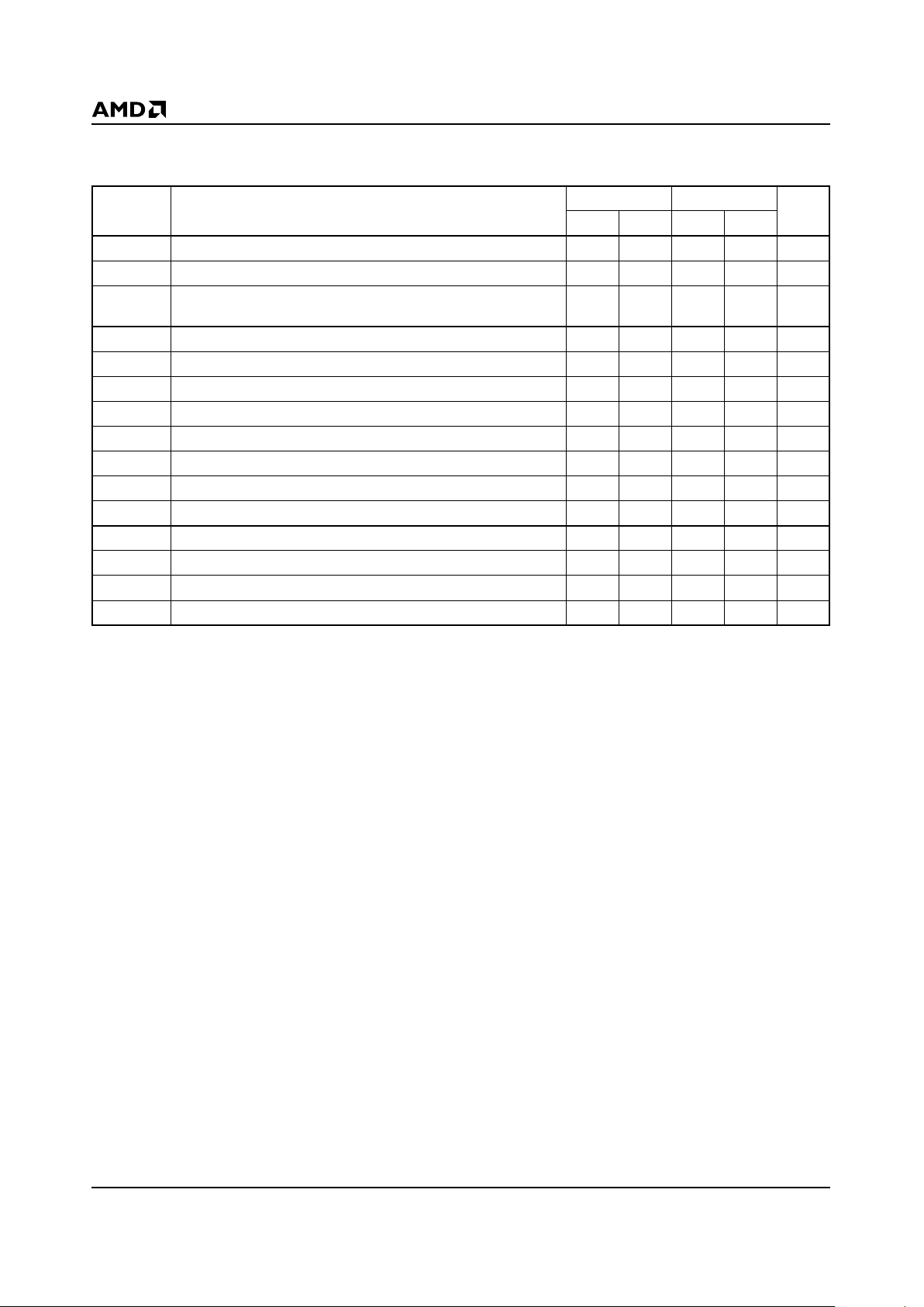
CAPACITANCE (Note 1)
Parameter
Symbol Parameter Description Test Conditions Typ Unit
C
IN
Input Capacitance V
IN
= 2.0 V
V
CC
= 5.0 V, TA = 25°C
f = 1 MHz
6pF
C
OUT
Output Capacitance V
OUT
= 2.0 V 8 pF
SWITCHING CHARACTERISTICS over COMMERCIAL operating ranges (Note 2)
Parameter
Symbol Parameter Description
-12 -15 -20
UnitMin Max Min Max Min Max
t
PD
Input, I/O, or Feedback to Combinatorial Output
(Note 3)
12 15 20 ns
t
S
Setup Time from Input, I/O, or
Feedback to Clock
D-type 7 10 13 ns
T-type 8 11 14 ns
t
H
Register Data Hold Time 0 0 0 ns
t
CO
Clock to Output (Note 3) 8 10 12 ns
t
WL
Clock Width
LOW 6 6 8 ns
t
WH
HIGH 6 6 8 ns
f
MAX
Maximum
Frequency
(Note 1)
External
Feedback
1/(t
S
+ tCO)
D-type 66.7 50 40 MHz
T-type 62.5 47.6 38.5 MHz
Internal Feedback (f
CNT
)
D-type 83.3 66.6 50 MHz
T-type 76.9 62.5 47.6 MHz
No
Feedback
1/(t
WL
+ tWH) 83.3 83.3 62.5 MHz
t
SL
Setup Time from Input, I/O, or Feedback to Gate 7 10 13 ns
t
HL
Latch Data Hold Time 0 0 0 ns
t
GO
Gate to Output 10 11 12 ns
t
GWL
Gate Width LOW 6 6 8 ns
t
PDL
Input, I/O, or Feedback to Output Through
Transparent Input or Output Latch
14 17 22 ns
t
SIR
Input Register Setup Time 2 2 2 ns
t
HIR
Input Register Hold Time 2 2.5 3 ns
t
ICO
Input Register Clock to Combinatorial Output 15 18 23 ns
t
ICS
Input Register Clock to Output Register
Setup
D-type 12 15 20 ns
T-type 13 16 21 ns
t
WICL
Input Register Clock Width
LOW 6 6 8 ns
t
WICH
HIGH 6 6 8 ns
f
MAXIR
Maximum Input Register
Frequency
1/(t
WICL
+ t
WICH
) 83.3 83.3 62.5 MHz
t
SIL
Input Latch Setup Time 2 2 2 ns
t
HIL
Input Latch Hold Time 2 2.5 3 ns

MACH211SP-12/15/20 (Com’l) 15
Notes:
1. These parameters are not 100% tested, but are evaluated at initial characterization and at any time the design is modified
where frequency may be affected.
2. See Switching Test Circuit for test conditions.
3. If a signal is powered-down, this parameter must be added to its respective high-speed parameter.
t
IGO
Input Latch Gate to Combinatorial Output 17 20 25 ns
t
IGOL
Input Latch Gate to Output Through Transparent
Output Latch
19 22 27 ns
t
SLL
Setup Time from Input, I/O , or Feedback Through
Transparent Input Latch to Output Latch Gate
91215ns
t
IGS
Input Latch Gate to Output Latch Setup 13 16 21 ns
t
WIGL
Input Latch Gate Width LOW 6 6 8 ns
t
PDLL
Input, I/O, or Feedback to Output Through
Transparent Input and Output Latches
16 19 24 ns
t
AR
Asynchronous Reset to Registered or Latched
Output
16 20 25 ns
t
ARW
Asynchronous Reset Width (Note 1) 12 15 20 ns
t
ARR
Asynchronous Reset Recovery Time (Note 1) 8 10 15 ns
t
AP
Asynchronous Preset to Registered or Latched
Output
16 20 25 ns
t
APW
Asynchronous Preset Width (Note 1) 12 15 20 ns
t
APR
Asynchronous Preset Recovery Time (Note 1) 8 10 15 ns
t
EA
Input, I/O, or Feedbac k to Output Enable (Note 1) 15 15 15 ns
t
ER
Input, I/O, or Feedback to Output Disable
(Note 1)
15 15 15 ns
t
LP
tPD Increase for Powered-down Macrocell
(Note 3)
10 10 10 ns
t
LPS
tS Increase for Po wered-do wn Macrocell (Note 3) 10 10 10 ns
t
LPCO
tCO Increase for Powered-down Macrocell
(Note 3)
000ns
t
LPEA
tEA Increase for Powered-down Macrocell
(Note 3)
10 10 10 ns
SWITCHING CHARACTERISTICS over COMMERCIAL operating ranges (Note 2)
(continued)
Parameter
Symbol Parameter Description
-12 -15 -20
UnitMin Max Min Max Min Max

16 MACH211SP-10/12 (Ind)
ABSOLUTE MAXIMUM RATINGS
Storage Temperature . . . . . . . . . . . . –65°C to +150°C
Ambient Temperature
with Power Applied. . . . . . . . . . . . . . –55°C to +125°C
Supply V oltage with
Respect to Ground. . . . . . . . . . . . . . .–0.5 V to +7.0 V
DC Input Voltage . . . . . . . . . . . .–0.5 V to VCC + 0.5 V
DC Output or
I/O Pin Voltage . . . . . . . . . . . . . .–0.5 V to V
CC
+ 0.5 V
Static Discharge Voltage . . . . . . . . . . . . . . . . . 2001 V
Latchup Current (TA = –40°C to +85°C). . . . . 200 mA
Stresses above those listed under Absolute Maximum
Ratings may cause permanent device failure. Functionality at
or above these limits is not implied. Exposure to Absolute
Maximum Ratings for extended periods may affect device
reliability. Programming conditions may differ.
OPERATING RANGES
Industrial (I) Devices
Temperature (TA)
Operating in Free Air. . . . . . . . . . . . . .–40°C to +85°C
Supply V oltage (VCC)
with Respect to Ground . . . . . . . . . . +4.5 V to +5.5 V
Operating ranges define those limits between which the
functionality of the device is guaranteed.
DC CHARACTERISTICS over INDUSTRIAL operating ranges unless otherwise specified
Notes:
1. These are absolute values with respect to device ground and all overshoots due to system and/or tester noise are included.
2. I/O pin leakage is the worst case of I
IL
and I
OZL
(or IIH and I
OZH
).
3. Not more than one output should be shorted at a time. Duration of the short-circuit should not exceed one second.
V
OUT
= 0.5 V has been chosen to avoid test problems caused by tester ground degradation.
4. This parameter is measured in low-power mode with a 16-bit up/down counter pattern. This pattern is programmed in each
PAL block and is capable of being loaded, enabled and reset.
5. This parameter is not 100% tested, but is evaluated at initial characterization and at any time the design is modified where
capacitance may be affected.
Parameter
Symbol Parameter Description Test Conditions Min Typ Max Unit
V
OH
Output HIGH Voltage IOH = –3.2 mA, VCC = Min, VIN = VIH or VIL2.4 V
V
OL
Output LOW Voltage IOL = 16 mA, VCC = Min, VIN = VIH or V
IL
0.5 V
V
IH
Input HIGH Voltage
Guaranteed Input Logical HIGH
Voltage for all Inputs (Note 1)
2.0 V
V
IL
Input LOW Voltage
Guaranteed Input Logical LOW
Voltage for all Inputs (Note 1)
0.8 V
I
IH
Input HIGH Leakage Current VIN = 5.25 V, VCC = Max (Note 2) 10 µA
I
IL
Input LOW Leakage Current VIN = 0 V, V
CC
= Max (Note 2) –10 µA
I
OZH
Off-State Output Leakage
Current HIGH
V
OUT
= 5.25 V, V
CC
= Max
V
IN
= V
IH
or VIL (Note 2)
10 µA
I
OZL
Off-State Output Leakage
Current LOW
V
OUT
= 0 V, V
CC
= Max
V
IN
= V
IH
or VIL (Note 2)
–10 µA
I
SC
Output Short-Circuit Current V
OUT
= 0.5 V, VCC = Max (Notes 3, 5) –30 –160 mA
I
CC
Supply Current (Static) VCC = 5 V, TA = 25°C, f = 0 MHz (Note 4) 40 mA
Supply Current (Active) VCC = 5 V, TA = 25°C, f = 1 MHz (Note 4) 45 mA

MACH211SP-10/12 (Ind) 17
CAPACITANCE (Note 1)
Parameter
Symbol Parameter Description Test Conditions Typ Unit
C
IN
Input Capacitance V
IN
= 2.0 V
V
CC
= 5.0 V, TA = 25°C
f = 1 MHz
6pF
C
OUT
Output Capacitance V
OUT
= 2.0 V 8 pF
SWITCHING CHARACTERISTICS over INDUSTRIAL operating ranges (Note 2)
Parameter
Symbol Parameter Description
-10 -12
UnitMin Max Min Max
t
PD
Input, I/O, or Feedback to Combinatorial Output (Note 3) 10 12 ns
t
S
Setup Time from Input, I/O, or Feedback to Clock
D-type 6.5 8 ns
T-type 7.5 9 ns
t
H
Register Data Hold Time 0 0 ns
t
CO
Clock to Output (Note 3) 6 7.5 ns
t
WL
Clock Width
LOW 5 6 ns
t
WH
HIGH 5 6 ns
f
MAX
Maximum
Frequency
(Note 1)
External Feedback 1/(t
S
+ tCO)
D-type 80 64 MHz
T-type 74 59 MHz
Internal Feedback (f
CNT
)
D-type 100 80 MHz
T-type 91 72.5 MHz
No Feedback 1/(tWL + tWH) 100 80 MHz
t
SL
Setup Time from Input, I/O, or Feedback to Gate 6.5 8 ns
t
HL
Latch Data Hold Time 0 0 ns
t
GO
Gate to Output 8 8.5 ns
t
GWL
Gate Width LOW 5 6 ns
t
PDL
Input, I/O, or Feedback to Output Through Transparent Input or
Output Latch
12 14.5 ns
t
SIR
Input Register Setup Time 2 2.5 ns
t
HIR
Input Register Hold Time 2 3 ns
t
ICO
Input Register Clock to Combinatorial Output 13 16 ns
t
ICS
Input Register Clock to Output Register Setup
D-type 10 12 ns
T-type 11 13 ns
t
WICL
Input Register Clock Width
LOW 5 6 ns
t
WICH
HIGH 5 6 ns
f
MAXIR
Maximum Input Register Frequency 1/(t
WICL
+ t
WICH
) 100 80 MHz
t
SIL
Input Latch Setup Time 2 2.5 ns
t
HIL
Input Latch Hold Time 2 3 ns
t
IGO
Input Latch Gate to Combinatorial Output 14 17 ns
t
IGOL
Input Latch Gate to Output Through Transparent Output Latch 16 19.5 ns

18 MACH211SP-10/12 (Ind)
Notes:
1. These parameters are not 100% tested, but are evaluated at initial characterization and at any time the design is modified
where capacitance may be affected.
2. See Switching Test Circuit for test conditions.
3. If a signal is powered-down, this parameter must be added to its respective high-speed parameter.
t
SLL
Setup Time from Input, I/O , or Feedbac k Through Transparent Input
Latch to Output Latch Gate
8.5 10.5 ns
t
IGS
Input Latch Gate to Output Latch Setup 11 13.5 ns
t
WIGL
Input Latch Gate Width LOW 5 6 ns
t
PDLL
Input, I/O, or Feedback to Output Through Transparent Input and
Output Latches
14 17 ns
t
AR
Asynchronous Reset to Registered or Latched Output 15 19.5 ns
t
ARW
Asynchronous Reset Width (Note 1) 10 12 ns
t
ARR
Asynchronous Reset Recovery Time (Note 1) 10 10 ns
t
AP
Asynchronous Preset to Registered or Latched Output 15 18 ns
t
APW
Asynchronous Preset Width (Note 1) 10 12 ns
t
APR
Asynchronous Preset Recovery Time (Note 1) 10 10 ns
t
EA
Input, I/O, or Feedback to Output Enable (Note 1) 15 15 ns
t
ER
Input, I/O, or Feedback to Output Disable (Note 1) 15 15 ns
t
LP
tPD Increase for Powered-down Macrocell (Note 3) 10 10 ns
t
LPS
tS Increase for Powered-down Macrocell (Note 3) 10 10 ns
t
LPCO
tCO Increase for Powered-down Macrocell (Note 3) 0 0 ns
t
LPEA
tEA Increase for Powered-down Macrocell (Note 3) 10 10 ns
SWITCHING CHARACTERISTICS over INDUSTRIAL operating ranges (Note 2) (continued)
Parameter
Symbol Parameter Description
-10 -12
UnitMin Max Min Max

MACH211SP-14/18/24 (Ind) 19
ABSOLUTE MAXIMUM RATINGS
Storage Temperature . . . . . . . . . . . . –65°C to +150°C
Ambient Temperature
with Power Applied. . . . . . . . . . . . . . –55°C to +125°C
Supply V oltage with
Respect to Ground. . . . . . . . . . . . . . .–0.5 V to +7.0 V
DC Input Voltage . . . . . . . . . . . .–0.5 V to VCC + 0.5 V
DC Output or
I/O Pin Voltage . . . . . . . . . . . . . .–0.5 V to V
CC
+ 0.5 V
Static Discharge Voltage . . . . . . . . . . . . . . . . . 2001 V
Latchup Current (TA = –40°C to 85°C). . . . . . 200 mA
Stresses above those listed under Absolute Maximum
Ratings may cause permanent device failure. Functionality at
or above these limits is not implied. Exposure to Absolute
Maximum Ratings for extended periods may affect device
reliability. Programming conditions may differ.
OPERATING RANGES
Industrial (I) Devices
Ambient Temperature (TA)
Operating in Free Air. . . . . . . . . . . . . .–40°C to +85°C
Supply V oltage (VCC)
with Respect to Ground . . . . . . . . . . +4.5 V to +5.5 V
Operating ranges define those limits between which the
functionality of the device is guaranteed.
DC CHARACTERISTICS over INDUSTRIAL operating ranges unless otherwise specified
Notes:
1. These are absolute values with respect to device ground and all overshoots due to system and/or tester noise are included.
2. I/O pin leakage is the worst case of I
IL
and I
OZL
(or IIH and I
OZH
).
3. Not more than one output should be shorted at a time. Duration of the short-circuit should not exceed one second.
V
OUT
= 0.5 V has been chosen to avoid test problems caused by tester ground degradation.
4. This parameter is measured in low-power mode with a 16-bit up/down counter pattern. This pattern is programmed in each
PAL block and is capable of being loaded, enabled and reset.
5. This parameter is not 100% tested, but is evaluated at initial characterization and at any time the design is modified where
capacitance may be affected.
Parameter
Symbol Parameter Description Test Conditions Min Typ Max Unit
V
OH
Output HIGH Voltage IOH = –3.2 mA, VCC = Min, VIN = VIH or VIL2.4 V
V
OL
Output LOW Voltage IOL = 16 mA, VCC = Min, VIN = VIH or V
IL
0.5 V
V
IH
Input HIGH Voltage
Guaranteed Input Logical HIGH
Voltage for all Inputs (Note 1)
2.0 V
V
IL
Input LOW Voltage
Guaranteed Input Logical LOW
Voltage for all Inputs (Note 1)
0.8 V
I
IH
Input HIGH Leakage Current VIN = 5.25 V, VCC = Max (Note 2) 10 µA
I
IL
Input LOW Leakage Current VIN = 0 V, V
CC
= Max (Note 2) –10 µA
I
OZH
Off-State Output Leakage
Current HIGH
V
OUT
= 5.25 V, V
CC
= Max
V
IN
= V
IH
or VIL (Note 2)
10 µA
I
OZL
Off-State Output Leakage
Current LOW
V
OUT
= 0 V, V
CC
= Max
V
IN
= V
IH
or VIL (Note 2)
–10 µA
I
SC
Output Short-Circuit Current V
OUT
= 0.5 V, VCC = Max (Notes 3, 5) –30 –160 mA
I
CC
Supply Current (Static) VCC = 5 V, TA = 25°C, f = 0 MHz (Note 4) 40 mA
Supply Current (Active) VCC = 5 V, TA = 25°C, f = 1 MHz (Note 4) 45 mA

20 MACH211SP-14/18/24 (Ind)
CAPACITANCE (Note 1)
Parameter
Symbol Parameter Description Test Conditions Typ Unit
C
IN
Input Capacitance V
IN
= 2.0 V
V
CC
= 5.0 V, TA = 25°C
f = 1 MHz
6pF
C
OUT
Output Capacitance V
OUT
= 2.0 V 8 pF
SWITCHING CHARACTERISTICS over INDUSTRIAL operating ranges (Note 2)
Parameter
Symbol Parameter Description
-14 -18 -24
UnitMin Max Min Max Min Max
t
PD
Input, I/O, or Feedback to Combinatorial Output
(Note 3)
14.5 18 24 ns
t
S
Setup Time from Input, I/O, or
Feedback to Clock
D-type 8.5 12 16 ns
T-type 10 13.5 17 ns
t
H
Register Data Hold Time 0 0 0 ns
t
CO
Clock to Output (Note 3) 10 12 14.5 ns
t
WL
Clock Width
LOW 7.5 7.5 10 ns
t
WH
HIGH 7.5 7.5 10 ns
f
MAX
Maximum
Frequency
(Note 1)
External
Feedback
1/(t
S
+ tCO)
D-type 53 40 32 MHz
T-type 50 38 30.5 MHz
Internal Feedback (f
CNT
)
D-type 61.5 53 38 MHz
T-type 57 44 34.5 MHz
No
Feedback
1/(t
WL
+ tWH) 66.5 66.5 50 MHz
t
SL
Setup Time from Input, I/O, or Feedback to Gate 8.5 12 16 ns
t
HL
Latch Data Hold Time 0 0 0 ns
t
GO
Gate to Output 12 13.5 14.5 ns
t
GWL
Gate Width LOW 7.5 7.5 10 ns
t
PDL
Input, I/O, or Feedback to Output Through
Transparent Input or Output Latch
17 20.5 26.5 ns
t
SIR
Input Register Setup Time 2.5 2.5 2.5 ns
t
HIR
Input Register Hold Time 3 3.5 4 ns
t
ICO
Input Register Clock to Combinatorial Output 18 22 28 ns
t
ICS
Input Register Clock to Output Register
Setup
D-type 14.5 18 24 ns
T-type 16 19.5 25.5 ns
t
WICL
Input Register Clock Width
LOW 7.5 7.5 10 ns
t
WICH
HIGH 7.5 7.5 10 ns
f
MAXIR
Maximum Input Register
Frequency
1/(t
WICL
+ t
WICH
) 66.5 66.5 50 MHz
t
SIL
Input Latch Setup Time 2.5 2.5 2.5 ns
t
HIL
Input Latch Hold Time 3 3.5 4 ns
t
IGO
Input Latch Gate to Combinatorial Output 20.5 24 30 ns

MACH211SP-14/18/24 (Ind) 21
Notes:
1. These parameters are not 100% tested, but are evaluated at initial characterization and at any time the design is modified
where capacitance may be affected.
2. See Switching Test Circuit for test conditions.
3. If a signal is powered-down, this parameter must be added to its respective high-speed parameter.
t
IGOL
Input Latch Gate to Output Through Transparent
Output Latch
23 26.5 32.5 ns
t
SLL
Setup Time from Input, I/O , or Feedback Through
Transparent Input Latch to Output Latch Gate
11 14.5 18 ns
t
IGS
Input Latch Gate to Output Latch Setup 16 19.5 25.5 ns
t
WIGL
Input Latch Gate Width LOW 7.5 7.5 10 ns
t
PDLL
Input, I/O, or Feedback to Output Through
Transparent Input and Output Latches
19.5 23 29 ns
t
AR
Asynchronous Reset to Registered or Latched
Output
19.5 24 30 ns
t
ARW
Asynchronous Reset Width (Note 1) 14.5 18 24 ns
t
ARR
Asynchronous Reset Recovery Time (Note 1) 10 12 18 ns
t
AP
Asynchronous Preset to Registered or Latched
Output
19.5 24 30 ns
t
APW
Asynchronous Preset Width (Note 1) 14.5 18 24 ns
t
APR
Asynchronous Preset Recovery Time (Note 1) 10 12 18 ns
t
EA
Input, I/O, or Feedbac k to Output Enable (Note 1) 14.5 18 24 ns
t
ER
Input, I/O, or Feedback to Output Disable
(Note 1)
14.5 18 24 ns
t
LP
tPD Increase for Powered-down Macrocell
(Note 3)
10 10 10 ns
t
LPS
tS Increase for Po wered-do wn Macrocell (Note 3) 10 10 10 ns
t
LPCO
tCO Increase for Powered-down Macrocell
(Note 3)
000ns
t
LPEA
tEA Increase for Powered-down Macrocell
(Note 3)
10 10 10 ns
SWITCHING CHARACTERISTICS over INDUSTRIAL operating ranges (Note 2) (continued)
Parameter
Symbol Parameter Description
-14 -18 -24
UnitMin Max Min Max Min Max

22 MACH211SP-7/10/12/15/20
TYPICAL ICC CHARACTERISTICS
V
CC
= 5 V, TA = 25°C
The selected “typical” pattern is a 16-bit up/down counter. This pattern is programmed in each PAL block and is capable of being
loaded, enabled, and reset.
Maximum frequency shown uses internal feedback and a D-type register.
100
150
50
0
0 102030405060708090
200
I
CC
(mA)
Frequency (MHz)
High Speed
Low Power
20405B-5

MACH211SP-7/10/12/15/20 23
TYPICAL THERMAL CHARACTERISTICS
Measured at 25°C ambient. These parameters are not tested.
Plastic θjc Considerations
The data listed for plastic θjc are for reference only and are not recommended for use in calculating junction temperatures. The
heat-flow paths in plastic-encapsulated devices are complex, making the θ
jc
measurement relative to a specific location on the
package surface. Tests indicate this measurement reference point is directly below the die-attach area on the bottom center of
the package. Furthermore, θ
jc
tests on packages are performed in a constant-temperature bath, keeping the package surface at
a constant temperature. Therefore, the measurements can only be used in a similar environment. TQFP thermal measurements
are taken with components on a six-layer printed circuit board.
Parameter
Symbol Parameter Description
Typ
UnitTQFP PLCC
θ
jc
Thermal impedance, junction to case 11.3 4 °C/W
θ
ja
Thermal impedance, junction to ambient 41 30.4 °C/W
θ
jma
Thermal impedance, junction to ambient
with air flow
200 lfpm air 35 18.5 °C/W
400 lfpm air 33.7 15.9 °C/W
600 lfpm air 32.6 13.5 °C/W
800 lfpm air 32 12.8 °C/W

24 MACH211SP-7/10/12/15/20
SWITCHING WAVEFORMS
Notes:
1. V
T
= 1.5 V.
2. Input pulse amplitude 0 V to 3.0 V.
3. Input rise and fall times 2 ns–4 ns typical.
20405B-6
Combinatorial Output
t
PD
Input, I/O, or
Feedback
Combinatorial
Output
V
T
V
T
20405B-7 20405B-8
Registered Output Latched Output
V
T
Input, I/O, or
Feedback
Registered
Output
t
S
t
CO
V
T
t
H
V
T
Clock
t
PDL
Input, I/O, or
Feedback
Latched
Out
Gate
V
T
t
HL
t
SL
t
GO
V
T
V
T
20405B-9 20405B-10
Clock Width Gate Width
t
WH
Clock
t
WL
Gate
t
GWL
V
T
20405B-11 20405B-12
Registered Input Input Register to Output Register Setup
V
T
Combinatorial
Output
t
SIR
t
ICO
V
T
t
HIR
V
T
Input
Register
Clock
Registered
Input
V
T
V
T
V
T
t
ICS
Output
Register
Clock
Input
Register
Clock
Registered
Input

MACH211SP-7/10/12/15/20 25
SWITCHING W A VEFORMS
Notes:
1. V
T
= 1.5 V.
2. Input pulse amplitude 0 V to 3.0 V.
3. Input rise and fall times 2 ns–4 ns typical.
20405B-13
Latched Input
Combinatorial
Output
Gate
t
HIL
t
SIL
t
IGO
Latched
In
V
T
V
T
V
T
20405B-14
Latched Input and Output
Latched
In
Output
Latch Gate
Latched
Out
t
SLL
t
PDLL
t
IGOL
t
IGS
Input
Latch Gate
V
T
V
T
V
T

26 MACH211SP-7/10/12/15/20
SWITCHING WAVEFORMS
Notes:
1. V
T
= 1.5 V.
2. Input pulse amplitude 0 V to 3.0 V.
3. Input rise and fall times 2 ns–4 ns typical.
20405B-15 20405B-16
Input Register Clock Width Input Latch Gate Width
t
WICH
Clock V
T
t
WICL
Input
Latch
Gate
t
WIGL
V
T
20405B-17 20405B-18
Asynchronous Reset Asynchronous Preset
V
T
V
T
t
ARW
V
T
t
AR
Input, I/O, or
Feedback
Registered
Output or
Latched
Output
Clock or
Input Latch
Gate
t
ARR
Input, I/O,
or Feedback
V
T
V
T
t
APW
V
T
t
AP
t
APR
Registered
Output or
Latched
Output
Clock or
Input Latch
Gate
20405B-19
Output Disable/Enable
V
T
V
T
Outputs
t
ER
t
EA
V
OH
– 0.5 V
V
OL
+ 0.5 V
Input, I/O, or
Feedback

MACH211SP-7/10/12/15/20 27
KEY TO SWITCHING WA VEFORMS
SWITCHING TEST CIRCUIT
* Switching several outputs simultaneously should be avoided for accurate measurement.
Specification S
1
C
L
Commercial
Measured Output ValueR
1
R
2
tPD, t
CO
Closed
35 pF
300 Ω 390 Ω
1.5 V
t
EA
Z → H: Open
Z → L: Closed
t
ER
H → Z: Open
L → Z: Closed
5 pF
H → Z: VOH – 0.5 V
L → Z: V
OL
+ 0.5 V
Must be
Steady
May
Change
from H to L
May
Change
from L to H
Does Not
Apply
Don’t Care,
Any Change
Permitted
Will be
Steady
Will be
Changing
from H to L
Will be
Changing
from L to H
Changing,
State
Unknown
Center
Line is HighImpedance
“Off” State
WAVEFORM INPUTS OUTPUTS
KS000010-PAL
20405B-20
C
L
Output
R
1
R
2
S
1
Test Point
5 V
28 MACH211SP-7/10/12/15/20
F
MAX
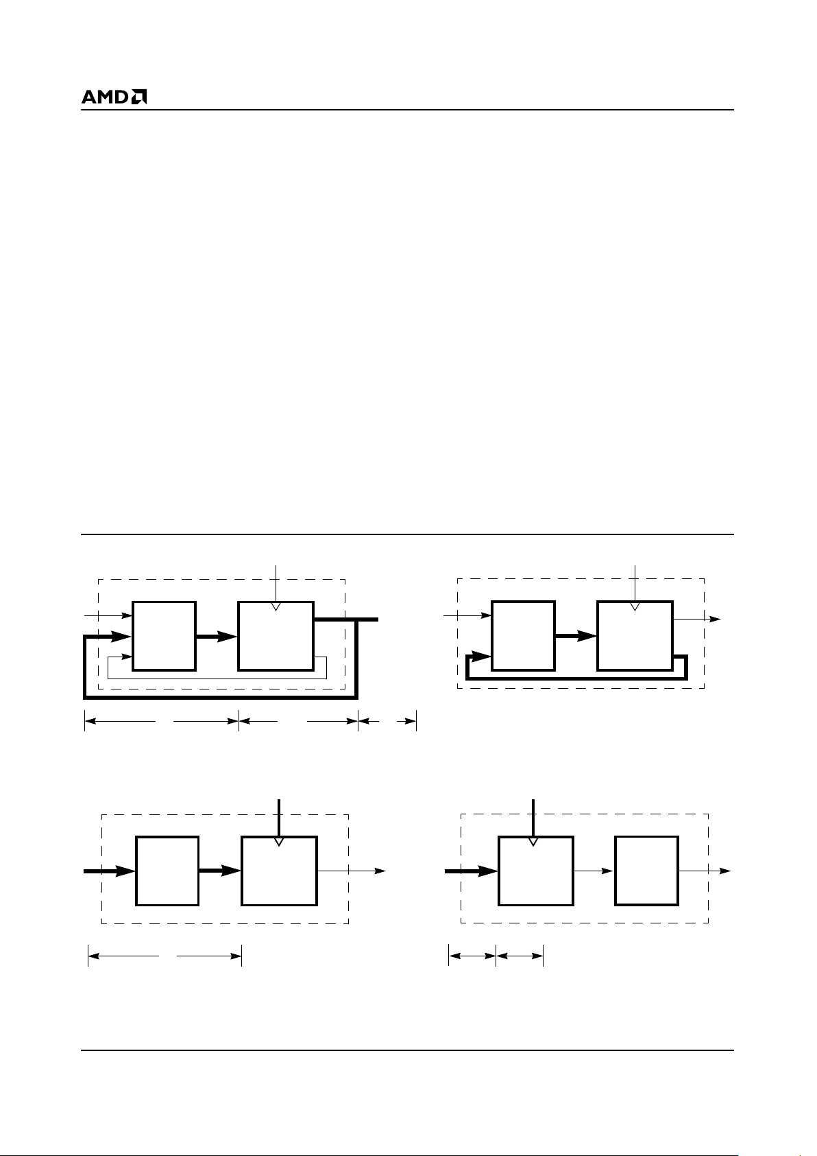
PARAMETERS
The parameter f
MAX
is the maximum clock rate at which
the device is guaranteed to operate. Because the flexibility inherent in programmable logic devices offers a
choice of clocked flip-flop designs, f
MAX
is specified for
three types of synchronous designs.
The first type of design is a state machine with feed-
back signals sent off-chip. This external feedback could
go back to the device inputs, or to a second de vice in a
multi-chip state machine. The slowest path defining the
period is the sum of the clock-to-output time and the
input setup time for the external signals (t
S
+ tCO). The
reciprocal, f
MAX
, is the maximum frequency with external feedback or in conjunction with an equiv alent speed
device. This f
MAX
is designated “f
MAX
external.”
The second type of design is a single-chip state machine with internal feedback only. In this case, flip-flop
inputs are defined by the device inputs and flip-flop outputs. Under these conditions, the period is limited by
the internal delay from the flip-flop outputs through the
internal feedback and logic to the flip-flop inputs. This
f
MAX
is designated “f
MAX
internal”. A simple internal
counter is a good example of this type of design; therefore, this parameter is sometimes called “f
CNT.
”
The third type of design is a simple data path application. In this case , input data is presented to the flip-flop
and clocked through; no feedback is employed. Under
these conditions, the period is limited by the sum of the
data setup time and the data hold time (t
S
+ tH). How-
ever , a lo wer limit f or the period of each f
MAX
type is the
minimum clock period (tWH + tWL). Usually, this minimum clock period determines the period for the third
f
MAX
, designated “f
MAX
no feedback.”
For devices with input registers , one additional f
MAX
pa-
rameter is specified: f
MAXIR
. Because this involves no
feedback, it is calculated the same way as f
MAX
no
feedback. The minimum period will be limited either by
the sum of the setup and hold times (t
SIR
+ t
HIR
) or the
sum of the clock widths (t
WICL
+ t
WICH
). The clock
widths are normally the limiting parameters, so that
f
MAXIR
is specified as 1/(t
WICL
+ t
WICH
). Note that if both
input and output registers are use in the same path, the
overall frequency will be limited by t
ICS
.
All frequencies except f
MAX
internal are calculated from
other measured AC parameters. f
MAX
internal is mea-
sured directly.
t
SIR
CLK
LOGIC
REGISTER
CLK
LOGIC
REGISTER
t
S
CLK
LOGIC
REGISTER
f
MAX
External; 1/(tS + tCO)f
MAX
Internal (f
CNT
)
f
MAX
No Feedback; 1/(tS + tH) or 1/(tWH + tWL)f
MAXIR
; 1/(t
SIR
+ t
HIR
) or 1/(t
WICL
+ t
WICH
)
t
S
t
CO
t
S
CLK
LOGIC
REGISTER
(SECOND
CHIP)
t
HIR
20405B-21

MACH211SP-7/10/12/15/20 29
ENDURANCE CHARACTERISTICS
The MACH families are manufactured using AMD’s advanced Electrically Erasable process. This technology
uses an EE cell to replace the fuse link used in bipolar
parts. As a result, the device can be erased and reprogrammed, a feature which allows 100% testing at the
factory.
Endurance Characteristics
Parameter
Symbol Parameter Description Min Units Test Conditions
t
DR
Min Pattern Data Retention Time
10 Years Max Storage Temperature
20 Years Max Operating Temperature
N Max Reprogramming Cycles 100 Cycles Normal Programming Conditions

30 MACH211SP-7/10/12/15/20
INPUT/OUTPUT EQUIVALENT SCHEMATICS
V
CC
ESD
Protection
1 kΩ
Input
V
CC
100 kΩ
Preload
Circuitry
Feedback
Input
I/O
V
CC
V
CC
100 kΩ
1 kΩ
20405B-22

MACH211SP-7/10/12/15/20 31
POWER-UP RESET
The MACH devices ha ve been designed with the capability to reset during system power-up. Following
power-up, all flip-flops will be reset to LOW . The output
state will depend on the logic polarity. This feature provides extra flexibility to the designer and is especially
valuable in simplifying state machine initialization. A
timing diagram and parameter table are shown below.
Due to the synchronous operation of the power-up
reset and the wide range of ways VCC can rise to its
steady state, two conditions are required to insure a
valid power-up reset. These conditions are:
1. The VCC rise must be monotonic.
2. Following reset, the clock input must not be driven
from LOW to HIGH until all applicable input and
feedback setup times are met.
Parameter Symbol Parameter Descriptions Max Unit
t
PR
Power-Up Reset Time 10 µs
t
S
Input or Feedback Setup Time
See Switching Characteristics
t
WL
Clock Width LOW
20405B-23
Power-Up Reset Waveform
t
PR
t
WL
t
S
4 V
V
CC
Power
Registered
Output
Clock

32 MACH211SP-7/10/12/15/20
DEVELOPMENT SYSTEMS (subject to change)
For more information on the products listed below, please consult the AMD FusionPLD Catalog.
MANUFACTURER SOFTWARE DEVELOPMENT SYSTEMS
Advanced Micro Devices, Inc.
P.O. Box 3453, MS 1028
Sunnyvale, CA 94088-3543
(800) 222-9323 or (408) 732-2400
MACHXL
®
Software
Ver. 3.0
Advanced Micro Devices, Inc.
P.O. Box 3453, MS 1028
Sunnyvale, CA 94088-3543
(800) 222-9323 or (408) 732-2400
Design Center/AMD Software
Advanced Micro Devices, Inc.
P.O. Box 3453, MS 1028
Sunnyvale, CA 94088-3543
(800) 222-9323 or (408) 732-2400
AMD-ABEL Software
Data I/O MACH Fitters
Advanced Micro Devices, Inc.
P.O. Box 3453, MS 1028
Sunnyvale, CA 94088-3543
(800) 222-9323 or (408) 732-2400
PROdeveloper/AMD
Software
PROsynthesis/AMD Software
Cadence Design Systems
555 River Oaks Pkwy
San Jose, CA 95134
(408) 943-1234
PLD™ Designer
Verilog, LeapFrog, RapidSim Simulators
Ver. 9504
Data I/O Corporation
10525 Willows Road N.E.
P.O. Box 97046
Redmond, WA 98073-9746
(800) 332-8246 or (206) 881-6444
ABEL™ Software
Synario™ Software
Mentor Graphics Corp.
8005 S.W. Boeckman Rd.
Wilsonville, OR 97070-7777
(800) 547-3000 or (503) 685-7000
PLDSynthesis™ II
QuickSim Simulator
MicroSim Corp.
20 Fairbanks
Irvine, CA 92718
(714) 770-3022
Design Center Software
MINC Incorporated
6755 Earl Drive, Suite 200
Colorado Springs, CO 80918
(800) 755-FPGA or (719) 590-1155
PLDesigner™-XL Software
SUSIE-CAD
10000 Nevada Highway, Suite 201
Boulder City, NV 89005
(702) 293-2271
SUSIE™ Simulator
Synopsys Logic Modeling
19500 NW Gibbs Dr.
P.O. Box 310
Beaverton, OR 97075
(503) 690-6900
SmartModel
®
Library
Teradyne EDA
321 Harrison Ave.
Boston, MA 02118
(800) 777-2432 or (617) 422-2793
MultiSIM Interactive Simulator
LASAR

MACH211SP-7/10/12/15/20 33
DEVELOPMENT SYSTEMS (subject to change) (continued)
Advanced Micro Devices is not responsible f or an y information relating to the products of third parties. The inclusion of such information is not a
representation nor an endorsement by AMD of these products.
MANUFACTURER SOFTWARE DEVELOPMENT SYSTEMS
Viewlogic Systems, Inc.
293 Boston Post Road West
Marlboro, MA 01752
(800) 442-4660 or (508) 480-0881
ViewPLD or PROPLD
(Requires PROSim Simulator MACH Fitter)
ViewSim Simulator
MANUFACTURER TEST GENERATION SYSTEM
Acugen Software, Inc.
427-3 Amherst St., Suite 391
Nashua, NH 03063
(603) 891-1995
ATGEN™ Test Generation Software
iNt GmbH
Busenstrasse 6
D-8033 Martinsried, Munich, Germany
(87) 857-6667
PLDCheck 90

34 MACH211SP-7/10/12/15/20
APPROVED PROGRAMMERS (subject to change)
For more information on the products listed below, please consult the AMD FusionPLD Catalog.
MANUFACTURER PROGRAMMER CONFIGURATION
Advin Systems, Inc.
1050-L East Duane Ave.
Sunnyvale, CA 94086
(408) 243-7000
Pilot U84
BP Microsystems
100 N. Post Oak Rd.
Houston, TX 77055-7237
(800) 225-2102 or (713) 688-4600
BP1148 BP1200 BP2100
Data I/O Corporation
10525 Willows Road N.E.
P.O. Box 97046
Redmond, WA 98073-9746
(800) 332-8246 or (206) 881-6444
UniSite™ Model 2900 Model 3900 AutoSite
Hi/Lo
4F, No. 2, Sec. 5, Ming Shoh E. Rd.
T aipei, Taiwan
ALL-07 FLEX-700
Logical Devices Inc./Digelec
692 S. Military Trail
Deerfield Beach, FL 33442
(800) 331-7766 or (305) 428-6868
ALLPRO™-88
SMS North America, Inc.
16522 NE 135th Place
Redmond, WA 98052
(800) 722-4122
or
SMS
lm Grund 15
D-7988 Vangen Im Allgau, Germany
07522-5018
Sprint Expert Multisite
Stag Microsystems Inc.
1600 Wyatt Dr. Suite 3
Santa Clara, CA 95054
(408) 988-1118
or
Stag House
Martinfield, Welwyn Garden City
Herfordshire UK AL7 1JT
707-332148
Stag Quazar
Stag Eclipse
System General
510 S. Park Victoria Dr.
Milpitas, CA 95035
(408) 263-6667
or
3F, No. 1, Alley 8, Lane 45
Bao Shing Rd., Shin Diau
T aipei, Taiwan
2-917-3005
T urpro-1 FX TX

MACH211SP-7/10/12/15/20 35
APPROVED ON-BOARD PROGRAMMERS
PROGRAMMER SOCKET ADAPTERS
(subject to change)
MANUFACTURER PROGRAMMER CONFIGURATION
Corelis, Inc.
12607 Hidden Creek Way, Suite H
Cerritos, California 70703
(310) 926-6727
JTAG PROG
Advanced Micro Devices
P.O. Box 3453, MS-1028
Sunnyvale, CA 94088-3453
(800) 222-9323
MACHpro
MANUFACTURER PART NUMBER
California Integration Technologies
656 Main Street
Placerville, CA 95667
(916) 626-6168
Contact Manufacturer
EDI Corporation
P.O. Box 366
Patterson, CA 95363
(209) 892-3270
Contact Manufacturer
Emulation Technology
2344 Walsh Ave., Bldg. F
Santa Clara, CA 95051
(408) 982-0660
Contact Manufacturer
Logical Systems Corp.
P.O. Box 6184
Syracuse, NY 13217-6184
(315) 478-0722
Contact Manufacturer
Procon T echnologies , Inc.
1333 Lawrence Expwy, Suite 207
Santa Clara, CA 95051
(408) 246-4456
Contact Manufacturer

36 MACH211SP-7/10/12/15/20
PHYSICAL DIMENSIONS*
PL 044
44-Pin Plastic Leaded Chip Carrier (measured in inches)
* For reference only. BSC is an ANSI standard for Basic Space Centering.
TOP VIEW
SEATING PLANE
.685
.695
.650
.656
Pin 1 I.D.
.685
.695
.650
.656
.026
.032
.050 REF
.042
.056
.062
.083
.013
.021
.590
.630
.500
REF
.009
.015
.165
.180
.090
.120
16-038-SQ
PL 044
DA78
6-28-94 ae
SIDE VIEW

MACH211SP-7/10/12/15/20 37
PHYSICAL DIMENSIONS
PQT044
44-Pin Thin Quad Flat Pack (measured in millimeters)
Trademarks
Copyright 1996 Advanced Micro Devices, Inc. All rights reserved.
AMD, the AMD logo, MACH, and PAL are registered trademarks of Advanced Micro Devices, Inc.
Bus-Friendly is a trademark of Advanced Micro Devices, Inc.
Product names used in this publication are for identification purposes only and may be trademarks of their respective companies.
1.00 REF.
1.20 MAX
11° – 13°
11° – 13°
0.80 BSC
44
1
0.95
1.05
11.80
12.20
9.80
10.20
11.80
12.20
9.80
10.20
0.30
0.45
16-038-PQT-2
PQT 44
7-11-95 ae
 Loading...