

Page 1

2014.12.15
www.altera.com
101 Innovation Drive, San Jose, CA 95134
I/O Buffer (ALTIOBUF) IP Core User Guide
UG-01024
Subscribe
The ALTIOBUF megafunction IP core implements either an I/O input buffer (ALTIOBUF_in), I/O
output buffer (ALTIOBUF_out), or I/O bidirectional buffer (ALTIOBUF_bidir). You can configure the IP
core through the IP Catalog and parameter editor in the Quartus® II software.
This user guide assumes that you are familiar with IP cores and how to configure them.
Related Information
Introduction to Altera IP Cores
Provides general information about Altera IP cores
ALTIOBUF Features
The ALTIOBUF IP core provides the following features:
• Capable of bus-hold circuitry
• Can enable differential mode
• Can specify open-drain output
• Can specify output enable port (oe)
• Can enable dynamic termination control ports for I/O bidirectional buffers
• Can enable series and parallel termination control ports for I/O output buffers and I/O bidirectional
buffers
• Can enable dynamic delay chains for I/O buffers
Send Feedback
I/O Buffer and Dynamic Delay Integration
Altera recommends that you use the ALTIOBUF IP core to utilize the I/O buffers for any purpose that
includes LVDS interfaces (using the ALTLVDS IP core), DDR interfaces (using the ALTDDIO_IN,
ALTDDIO_OUT, ALTDDIO_BIDIR, ALTDQ, ALTDQS, and ALTDQ_DQS IP cores) and dynamic onchip termination (OCT) control (using the ALTOCT IP core).
ALTIOBUF Common Application
The I/O buffers have standard capabilities such as bus-hold circuitry, differential mode, open-drain
output, and output enable port.
One of the key applications for this IP core is to have more direct termination control of the buffers. By
enabling series and parallel termination control ports for the I/O output buffers and I/O bidirectional
©
2014 Altera Corporation. All rights reserved. ALTERA, ARRIA, CYCLONE, ENPIRION, MAX, MEGACORE, NIOS, QUARTUS and STRATIX words and logos are
trademarks of Altera Corporation and registered in the U.S. Patent and Trademark Office and in other countries. All other words and logos identified as
trademarks or service marks are the property of their respective holders as described at www.altera.com/common/legal.html. Altera warrants performance
of its semiconductor products to current specifications in accordance with Altera's standard warranty, but reserves the right to make changes to any
products and services at any time without notice. Altera assumes no responsibility or liability arising out of the application or use of any information,
product, or service described herein except as expressly agreed to in writing by Altera. Altera customers are advised to obtain the latest version of device
specifications before relying on any published information and before placing orders for products or services.
ISO
9001:2008
Registered
Page 2
2
ALTIOBUF Common Application
buffers, you can connect these ports to the ALTOCT IP core to enable dynamic calibration for on-chip
termination.
The additional dynamic termination control ports allow control when series termination or parallel
termination are enabled for bidirectional buffers. Parallel termination needs to only be enabled when the
bidirectional I/O is receiving input. Otherwise, it needs to be disabled so that the output performance and
power dissipation is optimal.
Another key application for this IP core is for dynamic delay chain in the I/O buffer. Dynamic I/O delay
allows implementing automatic deskew, especially for memory interfaces, such as DDR3, which is
handled by the memory interface intellectual property (IP). You need to dynamically deskew and not
calculate manually because much of the skew can come from the I/O buffers of either the FPGA or the
other device the FPGA is interfacing with (for example, memory). Even if the trace lengths are matched,
there can still be electrical skew in the system. Also, this skew changes and can change from device to
device. Having the ability to deskew from the fabric allows you to remove uncertainties that would have to
be considered in the timing budget. This allows you to gain more timing margin, which allows higher
frequencies.
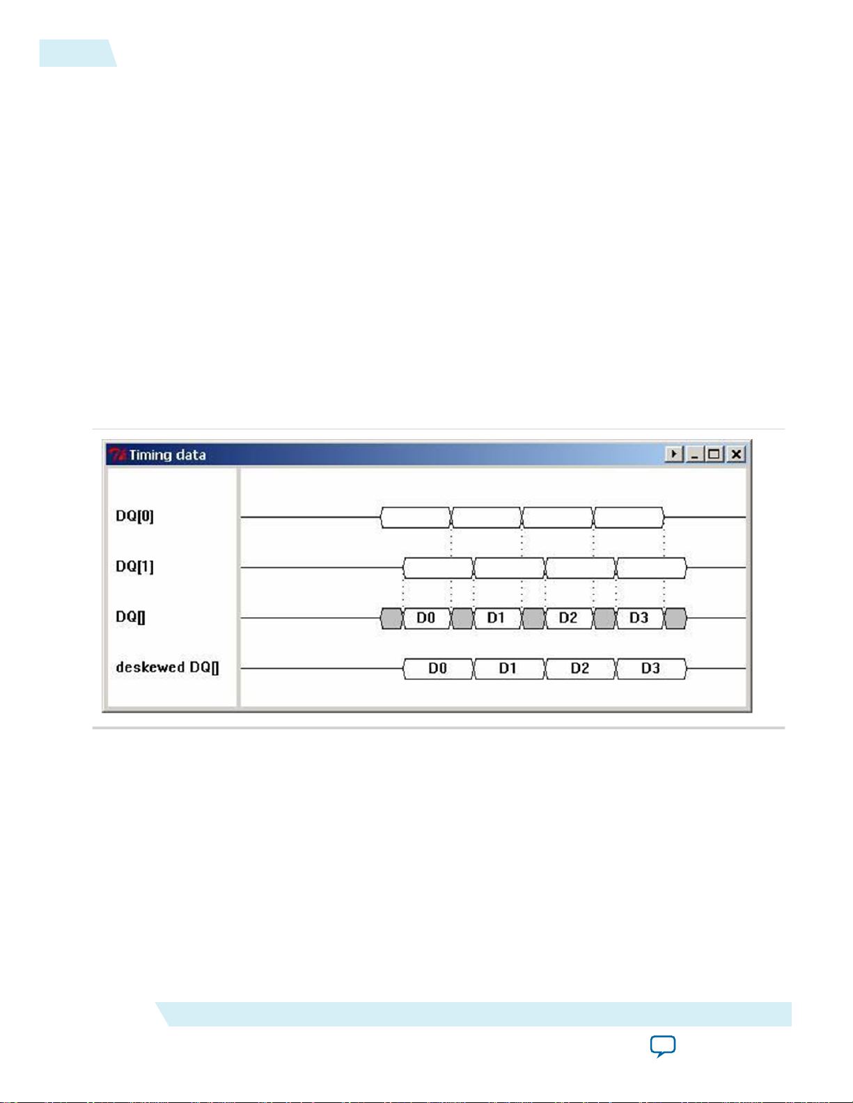
Figure 1: Example Illustrating Deskew
This figure shows an example of deskew.
UG-01024
2014.12.15
For example, if the input (or output) bus signals are DQ[0] and DQ[1], board trace skew, transmitter
device skew, or even FPGA package skew could cause signals that were initially aligned to become
misaligned. The third waveform shows the window available to the receiver for capturing the data. If
DQ[0] was delayed a bit to match DQ[1], a wider window would become available to the receiver.
Note:
To find the left and right edges of the data valid window, you need to do coarser adjustments (one
possible method is to use the new phase adjustment functionality of the PLL (ALTPLL IP core). The range
Altera Corporation
The deskew delay chains are not meant to find the middle of a data valid window, but just to
deskew the incoming (or outgoing) data to widen the overall window for a bus of inputs (or
outputs). To do this, you only need to align just one edge (for example, the left edge) of the data
valid window of all the pins.
I/O Buffer (ALTIOBUF) IP Core User Guide
Send Feedback
Page 3

acds
quartus - Contains the Quartus II software
ip - Contains the Altera IP Library and third-party IP cores
altera - Contains the Altera IP Library source code
<IP core name> - Contains the IP core source files
UG-01024
2014.12.15
of the deskew delay chains is only designed to compensate for a reasonable amount of board and package/
layout skew.
Related Information
ALTOCT IP Core User Guide
Provides information about connecting the ALTIOBUF ports to ALTOCT IP core.
Installing and Licensing IP Cores
The Altera IP Library provides many useful IP core functions for production use without purchasing an
additional license. You can evaluate any Altera® IP core in simulation and compilation in the Quartus® II
software using the OpenCore® evaluation feature. Some Altera IP cores, such as MegaCore® functions,
require that you purchase a separate license for production use. You can use the OpenCore Plus feature to
evaluate IP that requires purchase of an additional license until you are satisfied with the functionality and
performance. After you purchase a license, visit the Self Service Licensing Center to obtain a license
number for any Altera product.
Figure 2: IP Core Installation Path
Installing and Licensing IP Cores
3
Note: The default IP installation directory on Windows is <drive>:\altera\<version number>; on Linux it is
<home directory>/altera/ <version number>.
Related Information
• Altera Licensing Site
• Altera Software Installation and Licensing Manual
IP Catalog and Parameter Editor
The Quartus II IP Catalog (Tools > IP Catalog) and parameter editor help you easily customize and
integrate IP cores into your project. You can use the IP Catalog and parameter editor to select, customize,
and generate files representing your custom IP variation.
Note:
The IP Catalog lists IP cores available for your design. Double-click any IP core to launch the parameter
editor and generate files representing your IP variation. The parameter editor prompts you to specify an
IP variation name, optional ports, and output file generation options. The parameter editor generates a
top-level Qsys system file (.qsys) or Quartus II IP file (.qip) representing the IP core in your project. You
can also parameterize an IP variation without an open project.
The IP Catalog (Tools > IP Catalog) and parameter editor replace the MegaWizard™ Plug-In
Manager for IP selection and parameterization, beginning in Quartus II software version 14.0. Use
the IP Catalog and parameter editor to locate and paramaterize Altera IP cores.
I/O Buffer (ALTIOBUF) IP Core User Guide
Send Feedback
Altera Corporation
Page 4
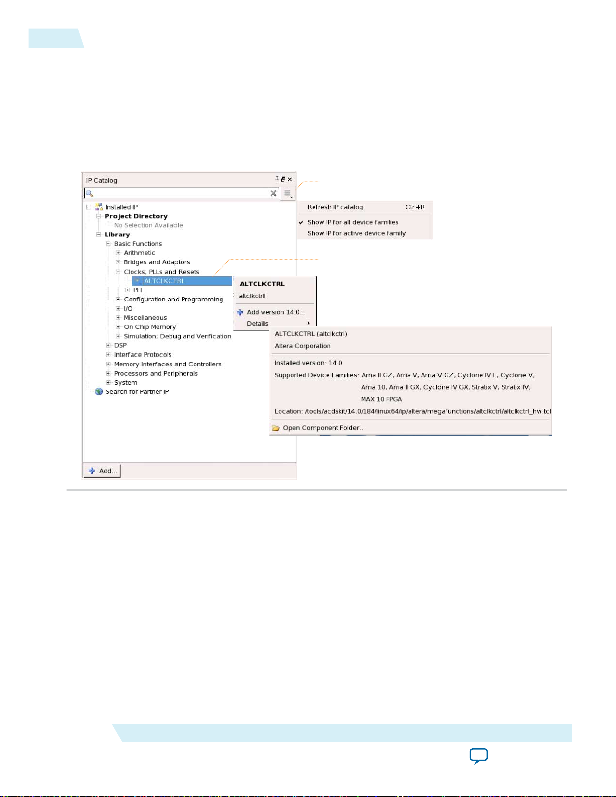
Search and filter IP for your target device
Double-click to customize, right-click for information
4
Using the Parameter Editor
Use the following features to help you quickly locate and select an IP core:
• Filter IP Catalog to Show IP for active device family or Show IP for all device families.
• Search to locate any full or partial IP core name in IP Catalog. Click Search for Partner IP, to access
partner IP information on the Altera website.
• Right-click an IP core name in IP Catalog to display details about supported devices, open the IP core's
installation folder, andor view links to documentation.
Figure 3: Quartus II IP Catalog
UG-01024
2014.12.15
Note: The IP Catalog is also available in Qsys (View > IP Catalog). The Qsys IP Catalog includes
exclusive system interconnect, video and image processing, and other system-level IP that are not
available in the Quartus II IP Catalog. For more information about using the Qsys IP Catalog, refer
to Creating a System with Qsys in the Quartus II Handbook.
Using the Parameter Editor
The parameter editor helps you to configure IP core ports, parameters, and output file generation options.
• Use preset settings in the parameter editor (where provided) to instantly apply preset parameter values
for specific applications.
• View port and parameter descriptions, and links to documentation.
• Generate testbench systems or example designs (where provided).
Altera Corporation
I/O Buffer (ALTIOBUF) IP Core User Guide
Send Feedback
Page 5
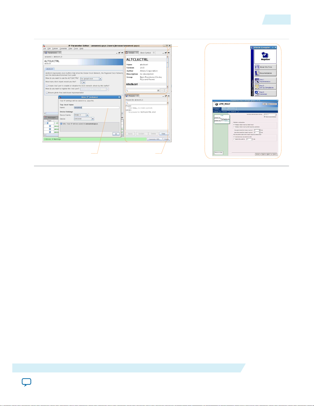
View IP port
and parameter
details
Apply preset parameters for
specific applications
Specify your IP variation name
and target device
Legacy parameter
editors
UG-01024
2014.12.15
Figure 4: IP Parameter Editors
Customizing and Generating IP Cores
5
Customizing and Generating IP Cores
You can customize IP cores to support a wide variety of applications. The Quartus II IP Catalog displays
IP cores available for the current target device. The parameter editor guides you to set parameter values
for optional ports, features, and output files.
To customize and generate a custom IP core variation, follow these steps:
1. In the IP Catalog (Tools > IP Catalog), locate and double-click the name of the IP core to customize.
The parameter editor appears.
2. Specify a top-level name for your custom IP variation. This name identifies the IP core variation files
in your project. If prompted, also specify the target Altera device family and output file HDL
preference. Click OK.
3. Specify the desired parameters, output, and options for your IP core variation:
• Optionally select preset parameter values. Presets specify all initial parameter values for specific
applications (where provided).
• Specify parameters defining the IP core functionality, port configuration, and device-specific
features.
• Specify options for generation of a timing netlist, simulation model, testbench, or example design
(where applicable).
• Specify options for processing the IP core files in other EDA tools.
4. Click Finish or Generate to generate synthesis and other optional files matching your IP variation
specifications. The parameter editor generates the top-level .qip or .qsys IP variation file and HDL files
I/O Buffer (ALTIOBUF) IP Core User Guide
Send Feedback
Altera Corporation
Page 6
6
Upgrading IP Cores
for synthesis and simulation. Some IP cores also simultaneously generate a testbench or example
design for hardware testing.
5. To generate a simulation testbench, click Generate > Generate Testbench System. Generate >
Generate Testbench System is not available for some IP cores.
6. To generate a top-level HDL design example for hardware verification, click Generate > HDL
Example. Generate > HDL Example is not available for some IP cores.
When you generate the IP variation with a Quartus II project open, the parameter editor automatically
adds the IP variation to the project. Alternatively, click Project > Add/Remove Files in Project to
manually add a top-level .qip or .qsys IP variation file to a Quartus II project. To fully integrate the IP
into the design, make appropriate pin assignments to connect ports. You can define a virtual pin to
avoid making specific pin assignments to top-level signals.
Note: By default, all unused pins are tied to ground. Altera recommends setting all unused pins to tri-
state because doing otherwise might cause interference. To set all unused pins to tri-state, in the
Quartus II software, click Assignments > Device > Device and Pin Options > Unused Pins
and select an item from the Reserve all unused pins list.
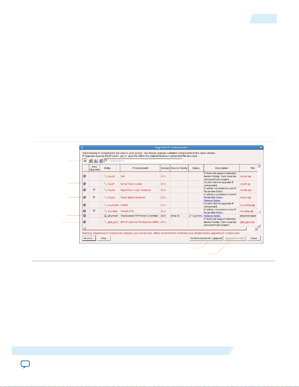
Upgrading IP Cores
UG-01024
2014.12.15
IP core variants generated with a previous version of the Quartus II software may require upgrading
before use in the current version of the Quartus II software. Click Project > Upgrade IP Components to
identify and upgrade IP core variants.
The Upgrade IP Components dialog box provides instructions when IP upgrade is required, optional, or
unsupported for specific IP cores in your design. You must upgrade IP cores that require it before you can
compile the IP variation in the current version of the Quartus II software. Many Altera IP cores support
automatic upgrade.
The upgrade process renames and preserves the existing variation file (.v, .sv, or .vhd) as <my_variant>_
BAK.v, .sv, .vhd in the project directory.
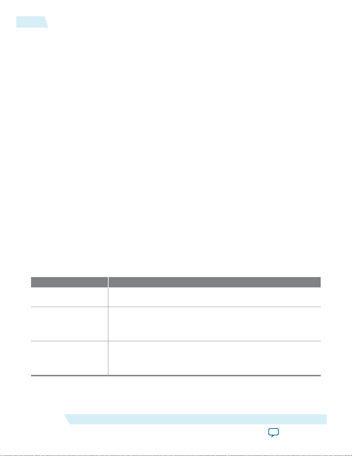
Table 1: IP Core Upgrade Status
IP Core Status Corrective Action
Required Upgrade IP
Components
Optional Upgrade IP
Components
You must upgrade the IP variation before compiling in the current version of
the Quartus II software.
Upgrade is optional for this IP variation in the current version of the Quartus
II software. You can upgrade this IP variation to take advantage of the latest
development of this IP core. Alternatively you can retain previous IP core
characteristics by declining to upgrade.
Upgrade Unsupported Upgrade of the IP variation is not supported in the current version of the
Quartus II software due to IP core end of life or incompatibility with the
current version of the Quartus II software. You are prompted to replace the
obsolete IP core with a current equivalent IP core from the IP Catalog.
Altera Corporation
I/O Buffer (ALTIOBUF) IP Core User Guide
Send Feedback
Page 7
Displays upgrade
status for all IP cores
in the Project
Upgrades all IP core that support “Auto Upgrade”
Upgrades individual IP cores unsupported by “Auto Upgrade”
Checked IP cores
support “Auto Upgrade”
Successful
“Auto Upgrade”
Upgrade
unavailable
Double-click to
individually migrate
UG-01024
2014.12.15
Upgrading IP Cores
Before you begin
• Archive the Quartus II project containing outdated IP cores in the original version of the Quartus II
software: Click Project > Archive Project to save the project in your previous version of the Quartus II
software. This archive preserves your original design source and project files.
• Restore the archived project in the latest version of the Quartus II software: Click Project > Restore
Archived Project. Click OK if prompted to change to a supported device or overwrite the project
database. File paths in the archive must be relative to the project directory. File paths in the archive
must reference the IP variation .v or .vhd file or .qsys file (not the .qip file).
1. In the latest version of the Quartus II software, open the Quartus II project containing an outdated IP
core variation. The Upgrade IP Components dialog automatically displays the status of IP cores in
your project, along with instructions for upgrading each core. Click Project > Upgrade IP
Components to access this dialog box manually.
2. To simultaneously upgrade all IP cores that support automatic upgrade, click Perform Automatic
Upgrade. The Status and Version columns update when upgrade is complete. Example designs
provided with any Altera IP core regenerate automatically whenever you upgrade the IP core.
Figure 5: Upgrading IP Cores
7
I/O Buffer (ALTIOBUF) IP Core User Guide
Example 1: Upgrading IP Cores at the Command Line
You can upgrade IP cores that support auto upgrade at the command line. IP cores that do not
support automatic upgrade do not support command line upgrade.
• To upgrade a single IP core that supports auto-upgrade, type the following command:
quartus_sh –ip_upgrade –variation_files <my_ip_filepath/my_ip>.<hdl>
<qii_project>
Example:
quartus_sh -ip_upgrade -variation_files mega/pll25.v hps_testx
Altera Corporation
Send Feedback
Page 8

8
ALTIOBUF Parameters
• To simultaneously upgrade multiple IP cores that support auto-upgrade, type the following
command:
quartus_sh –ip_upgrade –variation_files “<my_ip_filepath/my_ip1>.<hdl>;
<my_ip_filepath/my_ip2>.<hdl>” <qii_project>
Example:
quartus_sh -ip_upgrade -variation_files "mega/pll_tx2.v;mega/pll3.v"
hps_testx
Note: IP cores older than Quartus II software version 12.0 do not support upgrade.
Altera verifies that the current version of the Quartus II software compiles the
previous version of each IP core. The Altera IP Release Notes reports any verifica‐
tion exceptions for Altera IP cores. Altera does not verify compilation for IP cores
older than the previous two releases.
Related Information
Altera IP Release Notes
ALTIOBUF Parameters
UG-01024
2014.12.15
This table lists the options ALTIOBUF IP core parameters.
Table 2: ALTIOBUF IP Core Parameters: General Tab
Parameter Description
Currently selected device family: Specify the device family you want to use.
How do you want to configure this
module?
What is the number of buffers to be
instantiated?
Specify whether it is an input buffer, output buffer, or bidirec‐
tional buffer.
Specify the number of buffers to be used. This defines the size
of the buffer.
Use bus hold circuitry If enabled, the bus-hold circuitry can weakly hold the signal
on an I/O pin at its last-driven state. Available in input buffer,
output buffer, or bidirectional buffer.
Use differential mode If enabled, datain/datain_b is used for input buffers, both
dataout/dataout_b are used for output buffers, and both
dataio/dataio_b are used for bidirectional buffers.
Use open drain output If enabled, the open drain output enables the device to
provide system-level control signals (for example, interrupt
and write-enable signals) that can be asserted by multiple
devices in your system. This option is only available for
output buffers and bidirectional buffers.
Use output enable port(s) If enabled, there is a port used to control when the output is
Altera Corporation
enabled. This option is only available for output buffers and
bidirectional buffers.
I/O Buffer (ALTIOBUF) IP Core User Guide
Send Feedback
Page 9

UG-01024
2014.12.15
ALTIOBUF Parameters
Parameter Description
Use dynamic termination control(s) If enabled, this port receives the command to select either Rs
code (when input value = low) or Rt code (when input value =
high) from the core. Only enable Rt when the bi-directional I/
O is receiving input. Otherwise, it needs to be disabled so that
the output performance and power dissipation is optimal.
This option is available only for input and bidirectional
buffers.
An error is issued if parallel termination (Rt) is on and
dynamic termination control is not connected on a bidir pin.
An error is issued if parallel termination (Rt) is off and
dynamic termination control is connected on an input or
bidirectional pin.
Note that two I/Os in the same dynamic termination control
group needs to have the same dynamic termination control
signal. If the I/Os have separate dynamic termination control
signals, the Quartus II software produces a fitting error. A
dynamic termination control group is a group of pins that
share the same physical dynamic termination control signal
on the chip.
9
This option is not available in Cyclone III and Cyclone IV
devices.
Use series and parallel termination
controls
If enabled, this allows the series and parallel termination
control ports to be used. These ports can then be connected to
termination logic blocks to receive the Rs or Rt code from the
termination logic blocks.
This option is only available for output buffers and bidirec‐
tional buffers. The series and parallel termination control
ports are 14-bit wide for series or parallel termination.
For Cyclone III, Cyclone IV, and Cyclone V devices, this
option is available for output buffers and bidirectional buffers,
but not for input buffers. Only series termination is available.
The series termination control ports are 16-bit wide. The
width of these ports increases depending on the amount of
buffers instantiated.
Use left shift series termination control If enabled, you can use the left shift series termination control
to get the calibrated OCT Rs with half of the impedance value
of the external reference resistors connected to RUP and RDN
pins. This option is useful in applications which required both
25-Ω and 50-Ω calibrated OCT Rs at the same V
. For more
ccio
information, refer to I/O features chapter of the respective
device handbooks.
I/O Buffer (ALTIOBUF) IP Core User Guide
Send Feedback
Altera Corporation
Page 10

10
Using the Port and Parameter Definitions
Table 3: ALTIOBUF Parameters: Dynamic Delay Chains Tab
Parameter Description
Enable input buffer dynamic delay chain If enabled, the input or bidirectional buffer incorporates the
user-driven dynamic delay chain in the IP core; that is, the
IO_CONFIG and the input delay cell. Additional input ports are
enabled: io_config_clk, io_config_clkena, io_config_
update, and io_config_datain.
This option is not available for Cyclone III and Cyclone IV
devices.
Enable output buffer dynamic delay chain1If enabled, the output or bidirectional buffer incorporates the
user-driven dynamic delay chain in the IP core; that is, the
IO_CONFIG and the first output delay cell. Additional input
ports are enabled: io_config_clk, io_config_clkena, io_
config_update, and io_config_datain.
This option is not available for Cyclone III and Cyclone IV
devices.
UG-01024
2014.12.15
Enable output buffer dynamic delay chain2If enabled, the output buffer or bidirectional buffer incorpo‐
rates a user-driven dynamic delay chain in the IP core; that is,
the IO_CONFIG and the second output delay cell. Additional
input ports are enabled: io_config_clk, io_config_clkena,
io_config_update, and io_config_datain.
This option is not available for Cyclone III and Cyclone IV
devices.
Create a ‘clkena’ port If enabled, there is a port used to control when the configura‐
tion clock is enabled. This option is not available for Cyclone
III and Cyclone IV devices.
Using the Port and Parameter Definitions
Instead of using the parameter editor GUI, you can instantiate the IP core directly in your Verilog HDL,
VHDL, or AHDL code by calling the IP core and setting its parameters as you would any other module,
component, or subdesign.
Related Information
ALTIOBUF References on page 16
ALTIOBUF Functional Description
Altera Corporation
I/O Buffer (ALTIOBUF) IP Core User Guide
Send Feedback
Page 11

STRATIXIII_DELAY_CHAIN
STRATIXIII_DELAY_CHAIN
dataout[1..0]
input_dyn_delay_chaina_1
DATAIN
DELAYCTRLIN[3..0] DATAOUT
input_dyn_delay_chaina_0
DATAIN
DELAYCTRLIN[3..0] DATAOUT
STRATIXIII_IO_IBUF
ibufa_1
I
IBAR
O
ioconfiga_1
STRATIXIII_IO_CONFIG
DATAIN
CLK
ENA
PADTOINPUTREGISTERDELAYSETTING[3..0]
UPDATE
io_config_datain
io_config_clk
io_config_clkena[1..0]
io_config_update
datain[1..0]
datain_b[1..0]
STRATIXIII_IO_IBUF
ibufa_0
I
IBAR
O
ioconfiga_0
STRATIXIII_IO_CONFIG
DATAIN
CLK
ENA
PADTOINPUTREGISTERDELAYSETTING[3..0]
UPDATE
UG-01024
2014.12.15
ALTIOBUF Input, Output, and OE Paths
The three path types used with the I/O buffer in the delay chain architecture are input path, output path,
and oe path.
Dynamic delay chains are integrated in the input path for input and bidirectional buffers. Dynamic delay
chains are integrated in the output and oe paths for output and bidirectional buffers. This section
describes the dynamic delay chain-related components only.
All paths share a similar configuration in which the delay cells are getting their delay control signal from
the IO_CONFIG component. For the input path, the IO_CONFIG’s PADTOINPUTREGISTERDELAYSETTING
output port drives the DELAY_CHAIN’s (input delay cell) DELAYCTRLIN input port. For the output and
oe path, use the IO_CONFIG’s OUTPUTDELAYSETTING 1 and 2 output ports to drive the DELAYCTRLIN port
of the first and second output delay cells, respectively.
The number of delay chains needed is NUMBER_OF_CHANNELS. Each instance of the I/O buffer includes a
delay chain. Assume NUMBER_OF_CHANNELS is equal to ×. There must be × instances of input delay chain
for × input buffer, and 2× instances of the first output delay chain and 2× instances of the second output
delay chain output buffer because it uses the output and oe paths. The bidirectional buffer combines all
instances of the delay chains mentioned above.
Figure 6: Sample ALTIOBUF (Input Buffer Mode) Architecture when NUMBER_OF_CHANNELS = 2
ALTIOBUF Input, Output, and OE Paths
11
I/O Buffer (ALTIOBUF) IP Core User Guide
This figure shows the internal architecture of the ALTIOBUF IP core (input buffer mode) when
NUMBER_OF_CHANNELS is equal to 2 and the dynamic delay chain feature is enabled.
ALTIOBUF Input Buffer
The input buffer IP core uses the input path of the dynamic delay chain.
The datain and datain_b input ports of the ALTIOBUF IP core (input buffer mode) connect to the i
and ibar ports (if differential mode is enabled) of the input buffer, respectively. In the input path, the
value of the input buffer’s dataout port is passed into the input delay chain. The dataout port of the
ALTIOBUF IP core (input buffer mode) is the output of the dataout delay chain.
You must add a register external to the IP core, either a regular DFFE or a DDIO and connect its input to
the IP core’s dataout port.
Send Feedback
Altera Corporation
Page 12

STRATIXIII_IO_IBUF
ibufa_0
I O
datain[0..0]
io_config_datain
io_config_clk
ioconfiga_0
STRATIXIII_IO_CONFIG
io_config_clkena[0..0]
io_config_update
DATAIN
CLK
ENA
PADTOINPUTREGISTERDELAYSETTING[3..0]
UPDATE
STRATIXIII_DELAY_CHAIN
input_dyn_delay_chaina_0
DATAIN
DELAYCTRLIN[3..0] DATAOUT
dataout[0..0]
io_config_datain
io_config_clk
inddc01_w1:altiobuf_in
datain
io_config_clkena
io_config_update
ffclk
dataout
io_config_clk
io_config_datain
io_config_update dataout[0..0]
datain[0..0]
io_config_clkena[0..0]
PRN
CLR
D
Q
input_ff
ENA
12
Differential Mode Pin Naming Convention
Figure 7: Internal Architecture of ALTIOBUF (Input Buffer Mode)
This figure shows the internal architecture of the input buffer in the ALTIOBUF IP core.
Figure 8: ALTIOBUF (Input Buffer Mode) Connected to the External Flipflop
This figure shows how to connect the external register to the IP core.
UG-01024
2014.12.15
Differential Mode Pin Naming Convention
Use the following pin naming convention for differential mode:
<pin_name>[1..0]
Where:
• <pin_name>[0] is connected to the datain port
• <pin_name>[1] is connected to the datain_b port.
Note:
You must apply a differential I/O standard to both pins.
ALTIOBUF Output Buffer
The ALTIOBUF IP core (output buffer mode) uses the output and oe path of the dynamic delay chain,
where both share the same IO_CONFIG settings.
Contrary to the input path in the output and oe paths, you can add two optional registers, which are
external to the IP core. One is for the output path and the other is for the oe path.
Instead of connecting the input data to the datain port of the ALTIOBUF IP core (output buffer mode),
it is connected to the input of the registers that are external to the IP core. The output of the register is
then driven to the datain port of the first output delay chain port. In a similar way, the inverted input oe
is connected to the oe register that is external to the IP core, which drives the datain port of the first oe
delay chain port.
Altera Corporation
I/O Buffer (ALTIOBUF) IP Core User Guide
Send Feedback
Page 13

datain
io_config_clk
tc_out01:altiobuf_out
oe
outffclk
dataout
io_config_clk
io_config_datain
io_config_update dataout[0..0]
datain[0..0]
io_config_clkena[0..0]
PRN
CLR
D
Q
output_ff
ENA
PRN
CLR
D
Q
oe_ff
ENA
oe[0..0]
io_config_datain
io_config_clkena
io_config_update
io_config_datain
io_config_clk
ioconfiga_0
STRATIXIII_IO_CONFIG
STRATIXIII_DELAY_CHAIN
STRATIXIII_DELAY_CHAIN
STRATIXIII_DELAY_CHAIN
STRATIXIII_DELAY_CHAIN
STRATIXIII_IO_OBUF
io_config_clkena[0..0]
io_config_update
dataout[0..0]
oe[0..0]
datain[0..0]
DATAIN
CLK
ENA
OUTPUTDELAYSETTING[3..0]
OUTPUTDELAYSETTING[2..0]
UPDATE
output_dyn_delay_chain2a_0
output_dyn_delay_chain1a_0
DATAIN
DELAYCTRLIN[3..0] DATAOUT
oe_dyn_delay_chain1a_0
DATAIN
DELAYCTRLIN[3..0] DATAOUT
obufa_0
DATAIN
DELAYCTRLIN[3..0] DATAOUT
oe_dyn_delay_chain2a_0
DATAIN
DELAYCTRLIN[3..0]
I
OEDATAOUT
O
ioconfiga_0
STRATIXIII_IO_CONFIG
STRATIXIII_DELAY_CHAIN
STRATIXIII_DELAY_CHAIN
STRATIXIII_DELAY_CHAIN
STRATIXIII_DELAY_CHAIN
STRATIXIII_IO_OBUF
DATAIN
CLK
ENA
OUTPUTDELAYSETTING[3..0]
PADTOINPUTREGISTERDELAYSETTING[3..0]
OUTPUTDELAYSETTING[2..0]
UPDATE
output_dyn_delay_chain2a_0
output_dyn_delay_chain1a_0
DATAIN
DELAYCTRLIN[3..0] DATAOUT
oe_dyn_delay_chain1a_0
DATAIN
DELAYCTRLIN[3..0] DATAOUT
obufa_0
DATAIN
DELAYCTRLIN[3..0] DATAOUT
oe_dyn_delay_chain2a_0
DATAIN
DELAYCTRLIN[3..0]
I
OEDATAOUT
O
STRATIXIII_IO_IBUF
ibufa_0
I
O
STRATIXIII_DELAY_CHAIN
input_dyn_delay_chaina_0
DATAIN
DELAYCTRLIN[3..0] DATAOUT
dataio 1
UG-01024
2014.12.15
ALTIOBUF Bidirectional Buffer
Figure 9: ALTIOBUF (Output Buffer Mode) Connected with the External Flipflops
This figure shows how to connect the output and oe registers to the ALTIOBUF IP core.
Each of the output and oe delay chains are built from two cascaded output delay chains. The first output
delay chain’s dataout is connected to the second output delay chain’s datain. Depending on the
parameter chosen (use_out_dynamic_delay_chain1 or use_out_dynamic_delay_chain2), one or both
of the output delay chains can be dynamic. In this IP core, you can set the delay only for the dynamic
delay chains.
The second output delay chain’s dataout is connected to the output buffer’s i input port for the output
path and to the output buffer’s oe port for the oe path. Note that the output path and the oe path have
their own cascaded delay chains.
13
Figure 10: Internal Architecture of ALTIOBUF (Output Buffer Mode)
This figure shows the internal architecture of the ALTIOBUF IP core.
ALTIOBUF Bidirectional Buffer
The bidirectional buffer essentially combines the input buffer and the output buffer, incorporating the
input path, output path, and oe path.
By combining the input and output buffers, the output path and oe path are placed before the buffer and
the input path is placed after the buffer.
Figure 11: Internal Architecture of ALTIOBUF (Bidirectional Buffer Mode)
I/O Buffer (ALTIOBUF) IP Core User Guide
Send Feedback
Altera Corporation
Page 14

datain
io_config_clk
tc_bidir_01:altiobuf_bidir
oe
outffclk
dataout
io_config_clk
io_config_datain
io_config_update dataout[0..0]
datain[0..0]
dataio[0..0]
PRN
CLR
D
Q
output_ff
ENA
PRN
CLR
D
Q
oe_ff
ENA
io_config_clkena[0..0]
io_config_clkena
dataio
io_config_datain
io_config_update
inffclk
oe[0..0]
PRN
CLR
D
Q
input_ff
ENA
14
Dynamic Delay Chain Valid Values
By following these specifications, only the input path needs a register external to the IP core. The output
and oe registers that are added externally to the IP core are optional.
Figure 12: ALTIOBUF (Bidirectional Buffer Mode) Connected with External Flipflops
This figure shows an example of the ALTIOBUF IP core (bidirectional buffer mode) when output, oe, and
input path registers are used that are external to the IP core.
The external register placement is similar to the input/output buffers, where the output and oe registers
drive the datain and oe ports of the ALTIOBUF IP core (bidirectional buffer mode) and the dataout port
drives the input register.
UG-01024
2014.12.15
Altera Corporation
Note:
• The dynamic termination control path also contains output delay chain 1 and output delay
chain 2, which are not accessible through the ALTIOBUF IP core (bidirectional buffer mode).
When both the oe and dynamic termination control are used, the two signals (oe and dynamic
termination control) can be out of synchronization.
• It is not recommended to switch these two signals simultaneously.
Dynamic Delay Chain Valid Values
For information about the delay chain valid values, refer to the Programmable IOE Delay section of the
respective device handbook or data sheet.
Assignments Necessary For Dynamic Delay Chain Usage
If you utilize the dynamic delay chain for the I/O buffer IP core, a MEMORY_INTERFACE_DATA_PIN_GROUP
assignment to the I/O buffer block is necessary to enable it to go through fitting.
This is because the IP core utilizes the IO_CONFIG and DELAY_CHAIN blocks that are associated with the
use of DDR interfaces. Therefore, the Quartus II Fitter requires the assignment to determine the
placement of the blocks with the respective IO_xBUF block.
The format of the MEMORY_INTERFACE_DATA_PIN assignments generally appears as the following:
MEMORY_INTERFACE_DATA_PIN_GROUP {4|9|18|36} -from iobuf[0] -to iobuf[0]
MEMORY_INTERFACE_DATA_PIN_GROUP {4|9|18|36} -from iobuf[0] -to iobuf[1]
MEMORY_INTERFACE_DATA_PIN_GROUP {4|9|18|36} -from iobuf[0] -to iobuf[2]
….
MEMORY_INTERFACE_DATA_PIN_GROUP {4|9|18|36} -from iobuf[0] -to iobuf[n]
iobuf is the name of the buffer, either a stratixiii_io_obuf (for the output buffer) or
stratixiii_io_ibuf (for the input buffer). For the bidirectional buffer, either one is acceptable.
I/O Buffer (ALTIOBUF) IP Core User Guide
Send Feedback
Page 15

ioconfiga_0
obufa_0
output_dyn_delay_chain1a_0
oe_dyn_delay_chain1a_0
output_dyn_delay_chain2a_0
oe_dyn_delay_chain2a_0
DATAIN
CLK
ENA
UPDATE
OUTPUTDELAYSETTING1[3..0]
OUTPUTDELAYSETTING2[2..0]
DATAIN
DELAYCTRLIN[3..0]
DATAOUT
DATAIN
DELAYCTRLIN[3..0]
I
OE
O
DATAOUT
DATAIN
DELAYCTRLIN[3..0]
DATAOUT
DATAIN
DELAYCTRLIN[3..0]
DATAOUT
UG-01024
2014.12.15
Assignments Necessary For Dynamic Delay Chain Usage
Figure 13: Output Buffer
This figure shows an example of an output buffer.
To allow this particular design to be fit, add the following line in the Quartus Setting File (.qsf):
set_instance_assignment -name MEMORY_INTERFACE_DATA_PIN_GROUP 4 -from "u2|
test_output_iobuffer_iobuf_out_kk21:test_output_iobuffer_iobuf_out_kk21_component|
obufa_0" -to "u2|
test_output_iobuffer_iobuf_out_kk21:test_output_iobuffer_iobuf_out_kk21_component|
obufa_0"
You can also use the Assignment Editor to set the column fields as shown in the following table:
Table 4: Assigning the MEMORY_INTERFACE_DATA_PIN_GROUP Assignment
15
Column Setting
From u2|test_output_iobuffer_iobuf_out_kk21:test_output_iobuffer_iobuf_
out_kk21_component|obufa_0
To u2|test_output_iobuffer_iobuf_out_kk21:test_output_iobuffer_iobuf_
out_kk21_component|obufa_0
Assignment Name MEMORY_INTERFACE_DATA_PIN_GROUP
Value 4
Enable Yes
Then, set the Value field as shown in the following table:
Table 5: MEMORY_INTERFACE_DATA_PIN_GROUP Value
Number of Channels MEMORY_INTERFACE_DATA_PIN_GROUP Value
1–6 4
7–12 9
13–24 18
25–48 36
The design example associated with this user guide has this assignment.
Related Information
ALTDQ_DQS2 IP Core User Guide
Provides the I/O configuration block bit sequence for Arria V, Cyclone V, and Stratix V devices
I/O Buffer (ALTIOBUF) IP Core User Guide
Send Feedback
Altera Corporation
Page 16

16
ALTIOBUF References
ALTIOBUF References
Provides the signals, parameters, Verilog HDL prototype, and VHDL component declaration for
ALTIOBUF IP core.
Related Information
Using the Port and Parameter Definitions on page 10
ALTIOBUF Signals and Parameters: As Input Buffer
Table 6: ALTIOBUF (As Input Buffer) Input Ports
This table lists the input ports for the ALTIOBUF IP core (as input buffer).
Name Required Description
datain[] Yes The input buffer normal data input port.
Input port [NUMBER_OF_CHANNELS - 1..0] wide. The
input signal to the I/O output buffer element. For differen‐
tial signals, this port acquires the positive signal input.
UG-01024
2014.12.15
datain_b[] No The negative signal input of a differential signal to the I/O
input buffer element. Input port [NUMBER_OF_CHANNELS -
1..0] wide. When connected, the datain_b port is always
fed by a pad/port atom. This port is used only if the USE_
DIFFERENTIAL_MODE parameter value is TRUE.
io_config_datain No Input port that feeds the datain port of IO_CONFIG for user-
driven dynamic delay chain.
Input port used to feed input data to the serial load shift
register. The value is a 1-bit wire shared among all I/O
instances. This port is available only if the USE_IN_
DYNAMIC_DELAY_CHAIN parameter value is TRUE.
io_config_clk No Input clock port that feeds the IO_CONFIG for user-driven
dynamic delay chain. Input port used as the clock signal of
shift register block.
The maximum frequency for this clock is 30 MHz.
The value is a 1-bit wire shared among all I/O instances.
This port is available only if the USE_IN_DYNAMIC_DELAY_
CHAIN parameter value is TRUE.
Altera Corporation
I/O Buffer (ALTIOBUF) IP Core User Guide
Send Feedback
Page 17

UG-01024
2014.12.15
ALTIOBUF Signals and Parameters: As Input Buffer
Name Required Description
io_config_clkena[] No Input clock-enable that feeds the ena port of IO_CONFIG for
user-driven dynamic delay chain.
Input port [NUMBER_OF_CHANNELS - 1..0] wide. Input
port used as the clock enable signal of the shift register
block. This port is available only if the USE_IN_DYNAMIC_
DELAY_CHAIN parameter value is TRUE.
io_config_update No Input port that feeds the IO_CONFIG update port for user-
driven dynamic delay chain.
When asserted, the serial load shift register bits feed the
parallel load register. The value is a 1-bit wire shared among
all I/O instances. This port is available only if the USE_IN_
DYNAMIC_DELAY_CHAIN parameter value is TRUE.
Input signal for bidirectional I/Os.
Input port [NUMBER_OF_CHANNELS - 1..0] wide. When
specified, this port selects from the core either Rs code,
when the input value is LOW; or Rt code, when the input
value is HIGH. Enable Rt only when the bidirectional I/O is
dynamicterminationcontrol[]
No
receiving input. When the bidirectional I/O is not receiving
input, disable this port for optimal output performance and
power dissipation.
17
Value Rs Code Rt Code
0 1 0
1 0 1
Table 7: ALTIOBUF (As Input Buffer) Output Ports
This table shows the output ports for the ALTIOBUF IP core (as input buffer).
Name Required Description
dataout[] Yes Input buffer output port.
Input port [NUMBER_OF_CHANNELS - 1..0] wide. The
I/O input buffer element output.
I/O Buffer (ALTIOBUF) IP Core User Guide
Send Feedback
Altera Corporation
Page 18

18
ALTIOBUF Signals and Parameters: As Output Buffer
Table 8: ALTIOBUF (As Input Buffer) Parameters
This table lists the parameters for the ALTIOBUF IP core (as input buffer).
Name Required Type Description
ENABLE_BUS_HOLD No String Specifies whether the bus hold circuitry is
enabled. Values are TRUE and FALSE. When
set to TRUE, bus hold circuitry is enabled
and the previous value, instead of high
impedance, is assigned to the output port
when there is no valid input. If omitted, the
default is FALSE.
Currently, ENABLE_BUS_HOLD and USE_
DIFFERENTIAL_MODE cannot be used
simultaneously.
USE_DIFFERENTIAL_MODE No String Specifies whether the input buffer is
differential. Values are TRUE and FALSE.
When set to TRUE, the output is the
difference between the datain and datain_
b ports. If omitted, the default is FALSE.
UG-01024
2014.12.15
Currently, ENABLE_BUS_HOLD and USE_
DIFFERENTIAL_MODE cannot be used
simultaneously.
USE_IN_DYNAMIC_DELAY_CHAIN No String Specifies whether the input buffer incorpo‐
rates the user-driven dynamic delay chain
in the IP core, specifically, IO_CONFIG and
an input delay cell. Values are TRUE and
FALSE. If omitted, the default is FALSE.
NUMBER_OF_CHANNELS Yes Integer Specifies the number of I/O buffers that
must be instantiated. Value must be greater
than or equal to 1. A value of 1 indicates
that the buffer is a 1-bit port and accommo‐
dates wires; a value greater than 1 indicates
that the port can be connected to a bus of
width NUMBER_OF_CHANNELS.
USE_DYNAMIC_TERMINATION_
CONTROL
No String Specifies dynamic termination control.
Values are True and False. If omitted, the
default is False.
ALTIOBUF Signals and Parameters: As Output Buffer
Altera Corporation
I/O Buffer (ALTIOBUF) IP Core User Guide
Send Feedback
Page 19

UG-01024
2014.12.15
ALTIOBUF Signals and Parameters: As Output Buffer
Table 9: ALTIOBUF (As Output Buffer) Input Ports
This table lists the input ports for the ALTIOBUF IP core (as output buffer).
Name Required Description
datain[] Yes The output buffer input port.
Input port [NUMBER_OF_CHANNELS - 1..0]
wide. For differential signals, this port supplies
the positive signal input. Inputs are fed to the I/
O output buffer element.
io_config_datain No Input port that feeds the datain port of IO_
CONFIG for user-driven dynamic delay chain.
Input port used to feed input data to the serial
load shift register. The value is a 1-bit wire
shared among all I/O instances.
This port is available when the USE_OUT_
DYNAMIC_DELAY_CHAIN1 or USE_OUT_DYNAMIC_
DELAY_CHAIN2 parameter value is TRUE.
19
io_config_clk No Input clock port that feeds the IO_CONFIG for
user-driven dynamic delay chain.
Note that the maximum frequency for this clock
is 30 MHz.
Input port used as the clock signal of shift
register block. The value is a 1-bit wire shared
among all I/O instances.
This port is available when the USE_OUT_
DYNAMIC_DELAY_CHAIN1 or USE_OUT_DYNAMIC_
DELAY_CHAIN2 parameter value is TRUE.
io_config_clkena[] No Input clock-enable that feeds the ena port of IO_
CONFIG for user-driven dynamic delay chain.
Input port [NUMBER_OF_CHANNELS - 1..0]
wide. Input port used as the clock signal of shift
register block.
This port is available when the USE_OUT_
DYNAMIC_DELAY_CHAIN1 or USE_OUT_DYNAMIC_
DELAY_CHAIN2 parameter value is TRUE.
I/O Buffer (ALTIOBUF) IP Core User Guide
Send Feedback
Altera Corporation
Page 20

20
ALTIOBUF Signals and Parameters: As Output Buffer
Name Required Description
io_config_update No Input port that feeds the IO_CONFIG update port
for user-driven dynamic delay chain. When
asserted, the serial load shift register bits feed the
parallel load register. The value is a 1-bit wire
shared among all I/O instances.
This port is available when the USE_OUT_
DYNAMIC_DELAY_CHAIN1 or USE_OUT_DYNAMIC_
DELAY_CHAIN2 parameter value is TRUE.
oe[] No The output-enable source to the tri-state buffer.
Input port [NUMBER_OF_CHANNELS - 1..0]
wide. When the oe port is asserted, dataout and
dataout_b are enabled. When oe is deasserted,
both dataout and dataout_b are disabled. This
port is used only when the USE_OE parameter
value is TRUE. If omitted, the default is VCC.
seriesterminationcontrol[] No Receives the current state of the pull up and pull
down Rs control buses from a termination logic
block. Input port [WIDTH_STC * NUMBER_OF_
CHANNELS - 1..0] wide.
UG-01024
2014.12.15
Port is available only when the USE_TERMINA-
TION_CONTROL parameter value is TRUE.
seriesterminationcontrol_b No Receives the current state of the pull up and pull
down Rs control buses from a termination logic
block. Input port [WIDTH_STC * NUMBER_OF_
CHANNELS - 1..0] wide.
Port is available only when the USE_DIFFEREN-
TIAL_MODE parameter value is TRUE.
parallelterminationcontrol[] No Receives the current state of the pull up and pull
down Rt control buses from a termination logic
block. Input port [WIDTH_PTC * NUMBER_OF_
CHANNELS - 1..0] wide. The port is available
for Stratix III device families only. Supported in
Stratix® series only.
Port is available only when the USE_TERMINA-
TION_CONTROL parameter value is TRUE.
Altera Corporation
I/O Buffer (ALTIOBUF) IP Core User Guide
Send Feedback
Page 21

UG-01024
2014.12.15
Name Required Description
parallelterminationcontrol_b No Receives the current state of the pull up and pull
ALTIOBUF Signals and Parameters: As Output Buffer
down Rt control buses from a termination logic
block. Input port [WIDTH_PTC * NUMBER_OF_
CHANNELS - 1..0] wide. Port is available only
when the USE_DIFFERENTIAL_MODE parameter
value is TRUE. The port is available for Stratix
III device families only. Supported in Stratix
series only.
Port is available only when the USE_DIFFEREN-
TIAL_MODE parameter value is TRUE.
Table 10: ALTIOBUF (As Output Buffer) Output Ports
This table lists the output ports for the ALTIOBUF IP core (as output buffer).
Name Required Description
dataout[] Yes Output buffer output port. Output port
[NUMBER_OF_CHANNELS - 1..0] wide. The I/O
output buffer element output.
21
dataout_b[] No Differential output buffer-negative output.
Output port [NUMBER_OF_CHANNELS - 1..0]
wide. The I/O output buffer negative output.
Port is available only when the USE_DIFFEREN-
TIAL_MODE parameter value is TRUE.
Table 11: ALTIOBUF (As Output Buffer) Parameter
This table lists the parameters for the ALTIOBUF IP core (as output buffer).
Name Required Type Description
ENABLE_BUS_HOLD No String Specifies whether the bus hold
circuitry is enabled. Values are TRUE
and FALSE. When set to TRUE, bus hold
circuitry is enabled, and the previous
value, instead of high impedance, is
assigned to the output port when there
is no valid input. If omitted, the default
is FALSE.
Currently, ENABLE_BUS_HOLD and USE_
DIFFERENTIAL_MODE cannot be used
simultaneously.
I/O Buffer (ALTIOBUF) IP Core User Guide
Send Feedback
Altera Corporation
Page 22

22
ALTIOBUF Signals and Parameters: As Output Buffer
Name Required Type Description
USE_DIFFERENTIAL_MODE No String Specifies whether the output buffer
mode is differential. Values are TRUE
and FALSE. When set to TRUE, both the
dataout and dataout_b ports are
used. If omitted, the default is FALSE.
Currently, ENABLE_BUS_HOLD and USE_
DIFFERENTIAL_MODE cannot be used
simultaneously.
OPEN_DRAIN_OUTPUT No String Open drain mode. Values are TRUE and
FALSE. If omitted, the default is FALSE.
Note: Currently, OPEN_DRAIN_
OUTPUT and USE_DIFFERENTIAL_MODE cannot be used
simultaneously.
USE_TERMINATION_CONTROL No String Specifies series termination control
and parallel termination control.
Values are TRUE and FALSE. If omitted,
the default is FALSE. When this
parameter is used for Arria II GX
devices and the Cyclone series, only
series termination control is available.
Stratix series support both.
UG-01024
2014.12.15
USE_OUT_DYNAMIC_DELAY_CHAIN1 No String Specifies whether the output buffer
incorporates a user-driven dynamic
delay chain in the IP core, specifically,
IO_CONFIG and the first output delay
cell. Additional input ports are io_
config_clk, io_config_clkena, io_
config_update, and io_config_
datain. Values are TRUE and FALSE. If
omitted, the default is FALSE.
USE_OUT_DYNAMIC_DELAY_CHAIN2 No String Specifies whether the output buffer
incorporates a user-driven dynamic
delay chain in the IP core, specifically,
IO_CONFIG and the second output
delay cell. Additional input ports are
io_config_clk, io_config_clkena,
io_config_update, and io_config_
datain. Values are TRUE and FALSE.
If omitted, the default is FALSE.
Altera Corporation
I/O Buffer (ALTIOBUF) IP Core User Guide
Send Feedback
Page 23

UG-01024
2014.12.15
ALTIOBUF Signals and Parameters: As Bidirectional Buffer
Name Required Type Description
NUMBER_OF_CHANNELS Yes Integer Specifies the number of I/O buffers
that must be instantiated. Value must
be greater than or equal to 1. A value
of 1 indicates that the buffer is a 1-bit
port and accommodates wires. A value
greater than 1 indicates that the port
can be connected to a bus of width
NUMBER_OF_CHANNELS.
WIDTH_STC No Integer Specifies the width setting for the
series termination control bus.
WIDTH_PTC No Integer Specifies the width setting for the
parallel termination control bus.
USE_OE No String Specifies whether the oe port is used.
23
LEFT_SHIFT_SERIES_TERMINATION_
CONTROL
No String Values are True and False. If omitted,
the default is False. Available for all
supported devices except Cyclone
series device family.
PSEUDO_DIFFERENTIAL_MODE No String Specifies the pseudo differential mode.
Values are True and False. If omitted,
the default is False. Available only
when the USE_DIFFERENTIAL_MODE
parameter value is TRUE.
ALTIOBUF Signals and Parameters: As Bidirectional Buffer
Table 12: ALTIOBUF (As Bidirectional Buffer) Input Ports
This table lists the input ports for the ALTIOBUF IP core (as bidirectional buffer).
Name Required Description
datain[] Yes The input buffer input port. Input port [NUMBER_OF_
CHANNELS - 1..0] wide. The input signal to the I/O
output buffer element.
io_config_datain No Input port that feeds the datain port of IO_CONFIG for
user-driven dynamic delay chain. Input port used to
feed input data to the serial load shift register. The
value is a 1-bit wire shared among all I/O instances.
I/O Buffer (ALTIOBUF) IP Core User Guide
Send Feedback
This port is available only if the USE_IN_DYNAMIC_
DELAY_CHAIN, USE_OUT_DYNAMIC_DELAY_CHAIN1, or
USE_OUT_DYNAMIC_DELAY_CHAIN2 parameter value is
TRUE.
Altera Corporation
Page 24

24
ALTIOBUF Signals and Parameters: As Bidirectional Buffer
Name Required Description
io_config_clk No Input clock port that feeds the IO_CONFIG for user-
driven dynamic delay chain. The maximum
frequency for this clock is 30 MHz. Input port used as
the clock signal of shift register block. The value is a
1-bit wire shared among all I/O instances.
This port is available only if the USE_IN_DYNAMIC_
DELAY_CHAIN, USE_OUT_DYNAMIC_DELAY_CHAIN1, or
USE_OUT_DYNAMIC_DELAY_CHAIN2 parameter value is
TRUE.
io_config_clkena[] No Input clock-enable that feeds the ena port of IO_
CONFIG for user-driven dynamic delay chain. Input
port [NUMBER_OF_CHANNELS - 1..0] wide. Input
port used as the clock signal of the shift register block.
This port is available only if the USE_IN_DYNAMIC_
DELAY_CHAIN, USE_OUT_DYNAMIC_DELAY_CHAIN1, or
USE_OUT_DYNAMIC_DELAY_CHAIN2 parameter value is
TRUE.
UG-01024
2014.12.15
io_config_update No Input port that feeds the IO_CONFIG update port for
user-driven dynamic delay chain. When asserted, the
serial load shift register bits feed the parallel load
register. The value is a 1-bit wire shared among all I/
O instances.
This port is available only if the USE_IN_DYNAMIC_
DELAY_CHAIN, USE_OUT_DYNAMIC_DELAY_CHAIN1, or
USE_OUT_DYNAMIC_DELAY_CHAIN2 parameter value is
TRUE.
oe[] Yes The output-enable source to the tri-state buffer. Input
port [NUMBER_OF_CHANNELS - 1..0] wide. If
omitted, the default is VCC.
oe_b No The output-enable source to the tri-state buffer. Input
port [NUMBER_OF_CHANNELS - 1..0] wide. If
omitted, the default is VCC. Port is available only
when the USE_DIFFERENTIAL_MODE parameter value
is TRUE.
Altera Corporation
I/O Buffer (ALTIOBUF) IP Core User Guide
Send Feedback
Page 25

UG-01024
2014.12.15
Name Required Description
dynamicterminationcontrol[] No
dynamicterminationcontrol_b No
ALTIOBUF Signals and Parameters: As Bidirectional Buffer
Input signal for bidirectional I/Os. Input port
[NUMBER_OF_CHANNELS - 1..0] wide. When
specified, this port selects from the core either Rs
code, when the input value is LOW; or Rt code, when
the input value is HIGH. Enable Rt only when the
bidirectional I/O is receiving input. When the
bidirectional I/O is not receiving input, disable this
port for optimal output performance and power
dissipation.
Value Rs Code Rt Code
0 1 0
1 0 1
Input signal for bidirectional I/Os. Input port
[NUMBER_OF_CHANNELS - 1..0] wide. When
specified, this port selects from the core either Rs
code, when the input value is LOW; or Rt code, when
the input value is HIGH. Enable Rt only when the
bidirectional I/O is receiving input. When the
bidirectional I/O is not receiving input, disable this
port for optimal output performance and power
dissipation. Port is available only when the USE_
DIFFERENTIAL_MODE parameter value is TRUE.
25
Value Rs Code Rt Code
0 1 0
1 0 1
seriesterminationcontrol[] No Receives the current state of the pull up and pull
down Rs control buses from a termination logic
block. [WIDTH_STC * NUMBER_OF_CHANNELS -
1..0] wide. Port is applicable only when the USE_
TERMINATION_CONTROL parameter value is TRUE.
seriesterminationcontrol_b No Receives the current state of the pull up and pull
down Rs control buses from a termination logic
block. [WIDTH_STC * NUMBER_OF_CHANNELS -
1..0] wide. Port is applicable only when the USE_
TERMINATION_CONTROL parameter value is TRUE.
parallelterminationcontrol[] No Receives the current state of the pull up and pull
down Rt control buses from a termination logic
block. Input port [((WIDTH_PTC * NUMBER_OF_
CHANNELS) - 1)..0] wide. Port is applicable only
when the USE_TERMINATION_CONTROL parameter
value is TRUE.
I/O Buffer (ALTIOBUF) IP Core User Guide
Send Feedback
Altera Corporation
Page 26

26
ALTIOBUF Signals and Parameters: As Bidirectional Buffer
Name Required Description
parallelterminationcontrol_b No Receives the current state of the pull up and pull
down Rt control buses from a termination logic
block. Input port [((WIDTH_PTC * NUMBER_OF_
CHANNELS) - 1)..0] wide. Port is applicable only
when the USE_TERMINATION_CONTROL parameter
value is TRUE.
Table 13: ALTIOBUF (As Bidirectional Buffer) Output Ports
This table lists the output ports for ALTIOBUF IP core (as bidirectional buffer)
Name Required Description
dataout[] Yes Buffer output port. Output port [NUMBER_OF_
CHANNELS - 1..0] wide. The I/O output buffer
element output.
Table 14: ALTIOBUF (As Bidirectional Buffer) Bidirectional Ports
This table lists the bidirectional ports for ALTIOBUF IP core (as bidirectional buffer)
Name Required Description
UG-01024
2014.12.15
dataio[] Yes Bidirectional port that directly feeds a bidirectional
pin in the top-level design. Bidirectional port
[(NUMBER_OF_CHANNELS - 1)..0] wide.
dataio_b[] No Bidirectional DDR port that directly feeds a bidirec‐
tional pin in the top-level design. Bidirectional port
[(NUMBER_OF_CHANNELS - 1)..0] wide. The
negative signal input/output to/from the I/O buffer.
This port is used only if the use_differential_
mode_parameter is set to TRUE.
Table 15: ALTIOBUF (As Bidirectional Buffer) Parameter
This table lists the parameters for ALTIOBUF IP core (as bidirectional buffer)
Name Required Type Description
ENABLE_BUS_HOLD No String Specifies whether the bus hold circuitry is
enabled. Values are TRUE and FALSE.
When set to TRUE, bus hold circuitry is
enabled, and the previous value, instead of
high impedance, is assigned to the output
port when there is no valid input. If
omitted, the default is FALSE.
Altera Corporation
Currently, ENABLE_BUS_HOLD and USE_
DIFFERENTIAL_MODE cannot be used
simultaneously.
I/O Buffer (ALTIOBUF) IP Core User Guide
Send Feedback
Page 27

UG-01024
2014.12.15
ALTIOBUF Signals and Parameters: As Bidirectional Buffer
Name Required Type Description
USE_ DIFFERENTIAL_MODE No String Specifies whether the bidirectional buffer
is differential. Values are TRUE and FALSE.
When set to TRUE, the output is the
difference between the dataio and
dataio_b ports. If omitted, the default is
FALSE.
Currently, ENABLE_BUS_HOLD and USE_
DIFFERENTIAL_MODE cannot be used
simultaneously.
OPEN_DRAIN_OUTPUT No String Open drain mode. Values are TRUE and
FALSE. If omitted, the default is FALSE.
OPEN_DRAIN_OUTPUT and USE_DIFFERENTIAL_MODE cannot be used simultaneously.
USE_TERMINATION_CONTROL No String Specifies series termination control and
parallel termination control. Values are
TRUE and FALSE. If omitted, the default is
FALSE. When this parameter is used for
Arria II GX devices and Cyclone series,
only series termination control is available.
Stratix series supports both.
27
USE_DYNAMIC_TERMINATION_
CONTROL
No String Specifies dynamic termination control.
Values are TRUE and FALSE. If omitted, the
default is FALSE. An error is issued if
parallel termination (Rt) is on and
dynamic termination control is not
connected on a bidir pin. An error is
issued if Rt is off and dynamic termination
control is connected on an input or
bidirectional pin.
USE_IN_DYNAMIC_DELAY_CHAIN No String Specifies whether the input buffer incorpo‐
rates the user-driven dynamic delay chain
in the IP core, specifically, IO_CONFIG and
an input delay cell. Additional input ports
are io_config_clk, io_config_clkena,
io_config_update, and io_config_
datain. Values are TRUE and FALSE. If
omitted, the default is FALSE.
I/O Buffer (ALTIOBUF) IP Core User Guide
Send Feedback
Altera Corporation
Page 28

28
Verilog HDL Prototype
Name Required Type Description
USE_OUT_DYNAMIC_DELAY_CHAIN1 No String Specifies whether the output buffer
incorporates a user-driven dynamic delay
chain in the IP core, specifically, IO_
CONFIG and the first output delay cell.
Additional input ports are io_config_
clk, io_config_clkena, io_config_
update, and io_config_datain. Values
are TRUE and FALSE. If omitted, the default
is FALSE.
USE_OUT_DYNAMIC_DELAY_CHAIN2 No String Specifies whether the output buffer
incorporates a user-driven dynamic delay
chain in the IP core, specifically, IO_
CONFIG and the second output delay cell.
Additional input ports are io_config_
clk, io_config_clkena, io_config_
update, and io_config_datain. Values
are TRUE and FALSE. If omitted, the default
is FALSE.
UG-01024
2014.12.15
NUMBER_OF_CHANNELS Yes Integer Specifies the number of I/O buffers that
must be instantiated. Value must be
greater than or equal to 1. A value of 1
indicates that the buffer is a 1-bit port and
accommodates wires. A value greater than
1 indicates that the port can be connected
to a bus of width NUMBER_OF_CHANNELS.
WIDTH_STC No Integer Specifies the width setting for the series
termination control bus.
WIDTH_PTC No Integer Specifies the width setting for the parallel
termination control bus.
Verilog HDL Prototype
You can locate the Verilog HDL prototype in the Verilog Design File (.v) altera_mf.v in the <Quartus II
installation directory>\eda\synthesis directory.
VHDL Component Declaration
You can locate VHDL component declaration in the VHDL Design File (.vhd)
altera_mf_components.vhd in the <Quartus II installation directory>\libraries\vhdl\altera_mf
directory.
Altera Corporation
I/O Buffer (ALTIOBUF) IP Core User Guide
Send Feedback
Page 29

UG-01024
2014.12.15
VHDL LIBRARY-USE Declaration
The VHDL LIBRARY-USE declaration is not required if you use the VHDL Component Declaration.
LIBRARY altera_mf;
USE altera_mf.altera_mf_components.all;
Document Revision History
This table lists the revision history for this user guide.
Table 16: Document Revision History
Date Version Changes
December 2014 2014.12.15 Template update.
VHDL LIBRARY-USE Declaration
29
2014.06.30 4.0
• Replaced MegaWizard Plug-In Manager information
with IP Catalog.
• Added standard information about upgrading IP cores.
• Added standard installation and licensing information.
• Removed outdated device support level information. IP
core device support is now available in IP Catalog and
parameter editor.
• Removed all references to obsolete SOPC Builder tool.
June 2013 3.2
• Added “Differential Mode Pin Naming Convention”
• Updated the “Assignments Necessary For Dynamic
Delay Chain Usage” to include a link to the ALTDQ_
DQS2 Megafunction User Guide.
June 2013 3.1 Updated Table 2–1 on page 2–1 and Table 2–2 on page 2–2
to update the device family support.
February 2012 3.0
• Updated device support
• Added references to device handbook for delay chain
values
November 2010 2.1
• Updated to new template
• Updated ports and parameters
• Added prototypes and component declarations
December 2008 2.0
I/O Buffer (ALTIOBUF) IP Core User Guide
Send Feedback
• Added sentence to I/O Buffer and Dynamic Delay
Integration
• Added two last paragraph to Common Applications
• Added extra note to Table 3–5
• Remove figures
Altera Corporation
Page 30

30
Document Revision History
Date Version Changes
November 2007 1.0 Initial Release.
UG-01024
2014.12.15
Altera Corporation
I/O Buffer (ALTIOBUF) IP Core User Guide
Send Feedback
 Loading...