

Page 1

Hybrid Memory Cube Controller IP Core
User Guide
Last updated for Altera Complete Design Suite: 15.0
Subscribe
Send Feedback
UG-01152
2015.05.04
101 Innovation Drive
San Jose, CA 95134
www.altera.com
Page 2

TOC-2
About the Altera Hybrid Memory Cube Controller IP Core
Contents
About the Altera Hybrid Memory Cube Controller IP Core.............................1-1
Getting Started with the HMC Controller IP Core............................................2-1
HMC Controller IP Core Supported Features.........................................................................................1-2
HMC Controller IP Core Supported HMC Transaction Types............................................................1-3
Device Family Support................................................................................................................................1-4
IP Core Verification.....................................................................................................................................1-4
Simulation.........................................................................................................................................1-5
Hardware Testing.............................................................................................................................1-5
Performance and Resource Utilization.....................................................................................................1-5
Device Speed Grade Support......................................................................................................................1-6
Release Information.....................................................................................................................................1-6
Installing and Licensing IP Cores..............................................................................................................2-2
OpenCore Plus IP Evaluation........................................................................................................ 2-2
Specifying IP Core Parameters and Options............................................................................................2-2
HMC Controller IP Core Parameters....................................................................................................... 2-3
RX Mapping and TX Mapping Parameters..................................................................................2-5
Files Generated for Altera IP Cores...........................................................................................................2-8
Integrating Your IP Core in Your Design................................................................................................ 2-9
Pin Constraints.................................................................................................................................2-9
Required External Blocks..............................................................................................................2-10
Simulating Altera IP Cores in other EDA Tools................................................................................... 2-16
Understanding the Testbench..................................................................................................................2-18
Generating and Running the Testbench.................................................................................................2-18
Functional Description....................................................................................... 3-1
Altera Corporation
High Level Block Diagram..........................................................................................................................3-1
Interfaces Overview.....................................................................................................................................3-2
Application Interfaces..................................................................................................................... 3-2
HMC Interface..................................................................................................................................3-2
Interface to External I2C Master....................................................................................................3-3
Control and Status Register Interface........................................................................................... 3-3
Status and Debug Interface.............................................................................................................3-3
Transceiver Control Interfaces.......................................................................................................3-3
Clocking and Reset Structure.....................................................................................................................3-4
Initialization..................................................................................................................................................3-5
M20K ECC Support.....................................................................................................................................3-6
Flow Control.................................................................................................................................................3-7
Error Detection and Management.............................................................................................................3-7
Testing Features........................................................................................................................................... 3-8
Page 3

About the Altera Hybrid Memory Cube Controller IP Core
TOC-3
HMC Controller IP Core Signals........................................................................4-1
Application Interface Signals......................................................................................................................4-1
Application Request Interface........................................................................................................4-1
Application Response Interface..................................................................................................... 4-4
HMC Controller IP Core Data Path Example............................................................................. 4-7
HMC Interface Signals................................................................................................................................4-8
Signals on the Interface to the I2C Master................................................................................................4-9
Control and Status Interface Signals.......................................................................................................4-10
Status and Debug Signals..........................................................................................................................4-11
Clock and Reset Signals.............................................................................................................................4-12
Transceiver Reconfiguration Signals.......................................................................................................4-13
Signals on the Interface to the External PLLs........................................................................................ 4-15
HMC Controller IP Core Register Map..............................................................5-1
CONTROL Register.....................................................................................................................................5-2
XCVR_STATUS Register............................................................................................................................5-3
LANE_STATUS Register............................................................................................................................5-3
LINK_STATUS Register.............................................................................................................................5-4
ERROR_RESPONSE Register....................................................................................................................5-5
Interrupt Related Registers.........................................................................................................................5-5
Error and Retry Statistics Registers........................................................................................................... 5-9
HMC Controller IP Core Example Design.........................................................6-1
Additional Information......................................................................................A-1
HMC Controller IP Core User Guide Revision History....................................................................... A-1
How to Contact Altera............................................................................................................................... A-1
Typographic Conventions......................................................................................................................... A-2
Altera Corporation
Page 4
About the Altera Hybrid Memory Cube
FPGA/
ASIC
HMC Controller
100Gbps Ethernet
MAC
Hybrid Memory Cube
Ethernet
Link
FPGA/
ASIC
HMC Controller
100G Interlaken
Interlaken Link
www.altera.com
101 Innovation Drive, San Jose, CA 95134
Controller IP Core
2015.05.04
UG-01152
Subscribe
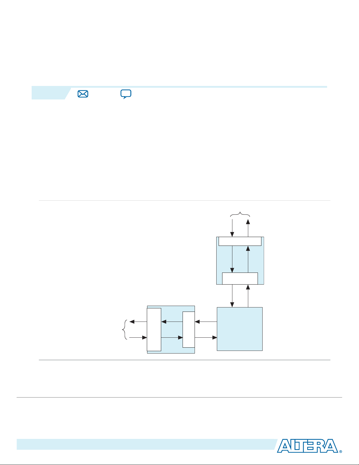
The Hybrid Memory Cube (HMC) specification defines a new type of memory device that provides a
significant increase in bandwidth and power efficiency over existing memory architectures. The HMC
specification targets high performance computers and next-generation networking equipment and
provides scalability for a wide range of applications.
The Altera® HMC Controller MegaCore® IP core enables easy access to external HMC devices. HMC
devices provide high bandwidth, reliable access to large amounts of memory with a small form factor, and
provide significant system cost savings in high performance, memory intensive applications. The HMC
Controller IP core provides a simple user interface through which you can communicate with an external
HMC device to incorporate these bandwidth and performance gains in your design.
Figure 1-1: Typical HMC Controller Application
Send Feedback
1
©
2015 Altera Corporation. All rights reserved. ALTERA, ARRIA, CYCLONE, ENPIRION, MAX, MEGACORE, NIOS, QUARTUS and STRATIX words and logos are
trademarks of Altera Corporation and registered in the U.S. Patent and Trademark Office and in other countries. All other words and logos identified as
trademarks or service marks are the property of their respective holders as described at www.altera.com/common/legal.html. Altera warrants performance
of its semiconductor products to current specifications in accordance with Altera's standard warranty, but reserves the right to make changes to any
products and services at any time without notice. Altera assumes no responsibility or liability arising out of the application or use of any information,
product, or service described herein except as expressly agreed to in writing by Altera. Altera customers are advised to obtain the latest version of device
specifications before relying on any published information and before placing orders for products or services.
ISO
9001:2008
Registered
Page 5

1-2
HMC Controller IP Core Supported Features
Related Information
HMC Specification 1.1
The HMC specification is available for download from the Hybrid Memory Cube Consortium web page.
HMC Controller IP Core Supported Features
The Altera HMC Controller IP core offers the following features:
• Communicates through Altera high-speed transceivers with an external HMC device compliant with
the HMC Specification 1.1.
• Communicates with the HMC device at per-lane rates of 10 Gbps or 12.5 Gbps.
• Features Avalon® Memory-Mapped (Avalon-MM) interface to access control and status registers.
• Supports selection of a full-width variation that connects to 16 lanes of an HMC device, or a half-width
variation that connects to 8 lanes of an HMC device.
• Full-width IP core variations feature a simple 512-bit client data interface, and support memory
READ and WRITE transactions with payloads of 16, 32, 64, and 128 bytes.
• Half-width IP core variations feature a simple 256-bit client data interface, and support memory
READ and WRITE transactions with payloads of 16, 32, 48, 64, 80, 96, 112, and 128 bytes.
• Supports posted and non-posted versions of ATOMIC transactions, BIT WRITE transactions, and
WRITE transactions.
• Supports MODE READ and MODE WRITE transactions.
• Supports Response Open Loop Mode for receive (RX) flow control to decrease device resource
requirements.
• Supports token-based transmit (TX) flow control.
• Supports poisoned packets.
• Supports reordering of transceiver lanes for board-design flexibility.
• Supports link training sequence and provides word alignment, lane alignment, and transceiver status
information in real time.
• Provides fast simulation support.
• Provides real-time error statistics.
• Provides hardware reset control.
• Optionally supports ADME direct access to transceiver registers through the Quartus II System
Console.
• Provides option to include ECC support in all M20K memory blocks configured in the IP core.
UG-01152
2015.05.04
To support multi-link connection to the HMC device in your design, you can configure multiple HMC
Controllers to communicate with the same HMC device through separate HMC links.
For the detailed HMC specification refer to the HMC Specification 1.1.
Related Information
Hybrid Memory Cube Consortium
The HMC Specification 1.1 is available on the Hybrid Memory Cube Consortium website.
Altera Corporation
About the Altera Hybrid Memory Cube Controller IP Core
Send Feedback
Page 6

UG-01152
2015.05.04
HMC Controller IP Core Supported HMC Transaction Types
HMC Controller IP Core Supported HMC Transaction Types
The Altera HMC Controller IP core supports all HMC transactions. The full-width variations require that
you specify READ transactions and posted and non-posted WRITE transactions with a payload size of 16,
32, 64, or 128 bytes. Half-width variations support all payload sizes described in the HMC Specification
v1.1.
HMC Controller To HMC Device Packet Types
The HMC Controller IP core generates the following packet types on the link to the HMC device:
• NULL FLIT
• PRET (single FLIT packet)
• IRTRY (single FLIT packet)
• READ request (single FLIT packet)
• 16-byte WRITE or Posted WRITE request (2-FLIT packet)
• 32-byte WRITE or Posted WRITE request (3-FLIT packet)
• 48-byte WRITE or Posted WRITE request (4-FLIT packet) (half-width IP core only)
• 64-byte WRITE or Posted WRITE request (5-FLIT packet)
• 80-byte WRITE or Posted WRITE request (6-FLIT packet) (half-width IP core only)
• 96-byte WRITE or Posted WRITE request (7-FLIT packet) (half-width IP core only)
• 112-byte WRITE or Posted WRITE request (8-FLIT packet) (half-width IP core only)
• 128-byte WRITE or Posted WRITE request (9-FLIT packet)
• BIT WRITE or Posted BIT WRITE request (2-FLIT packet)
• MODE READ request (single FLIT packet)
• MODE WRITE request (2-FLIT packet)
• Dual 8-byte ADD IMMEDIATE or Posted Dual 8-byte ADD IMMEDIATE request (2-FLIT packet)
• Single 16-byte ADD IMMEDIATE or Posted Single 16-byte ADD IMMEDIATE request (2-FLIT
packet)
1-3
The HMC Controller IP core operates in the Response Open Loop Mode and therefore does not generate
TRET packets.
HMC Device to HMC Controller Packet Types
The HMC Controller IP core can process the following packet types generated by the HMC device:
• NULL FLIT
• PRET (single FLIT packet)
• TRET (single FLIT packet)
• IRTRY (single FLIT packet)
• ERROR response (single FLIT packet)
• WRITE response (single FLIT packet)
• 16-byte READ response (2-FLIT packet)
• 32-byte READ response (3-FLIT packet)
• 48-byte READ response (4-FLIT packet) (half-width IP core only)
• 64-byte READ response (5-FLIT packet)
• 80-byte READ response (6-FLIT packet) (half-width IP core only)
• 96-byte READ response (7-FLIT packet) (half-width IP core only)
• 112-byte READ response (8-FLIT packet) (half-width IP core only)
About the Altera Hybrid Memory Cube Controller IP Core
Altera Corporation
Send Feedback
Page 7

1-4
Device Family Support
• 128-byte READ response (9-FLIT packet)
• MODE READ response (2-FLIT packet)
• MODE WRITE response (single FLIT packet)
The HMC Controller IP core does not process other packet types. Reception of any other packet type
might cause the IP core to fail.
Device Family Support
The following table lists the device support level definitions for Altera IP cores.
Table 1-1: Altera IP Core Device Support Levels
FPGA Device Families
Preliminary support — The core is verified with preliminary timing models for this device family. The IP
core meets all functional requirements, but might still be undergoing timing analysis for the device family. It
can be used in production designs with caution.
Final support — The IP core is verified with final timing models for this device family. The IP core meets all
functional and timing requirements for the device family and can be used in production designs.
UG-01152
2015.05.04
The following table shows the level of support offered by the HMC Controller IP core for each Altera
device family.
Table 1-2: HMC Controller IP Core Device Family Support
Device Family Support
Arria 10 Preliminary
All other device families No support
IP Core Verification
Before releasing a version of the HMC Controller IP core, Altera runs comprehensive regression tests in
the current version of the Quartus® II software. The HMC Controller IP Core is tested in simulation and
hardware to confirm functionality.
Related Information
Knowledge Base Errata for HMC Controller IP core
Exceptions to functional correctness are documented in the HMC Controller IP core errata.
Altera IP Release Notes
Changes to the HMC Controller IP core are noted in the Altera IP Release Notes starting from the
Quartus II software v15.0.
Altera Corporation
About the Altera Hybrid Memory Cube Controller IP Core
Send Feedback
Page 8

UG-01152
2015.05.04
Simulation
Altera performs the following tests on the HMC Controller IP core in simulation, using the Micron HMC
BFM:
• Constrained random tests that cover randomized legal payload sizes and contents
• Assertion based tests to confirm proper behavior of the IP core with respect to the specification
• Extensive coverage of packet retry functionality
Constrained random techniques generate appropriate stimulus for the functional verification of the IP
core. Altera monitors line, expression, and assertion coverage metrics to ensure that all important features
are verified.
Hardware Testing
Altera performs hardware testing of the key functions of the HMC Controller IP core. The Altera
hardware tests of the HMC Controller IP core also ensure reliable solution coverage for hardware related
areas such as performance, link initialization, and reset recovery.
Altera performs hardware testing on the Arria 10 GX FPGA Development Kit with an HMC mezannine
card. A Micron HMC 15G-SR device on the mezzannine card is connected to the development board
through FMC connectors.
Simulation
1-5
Performance and Resource Utilization
Table 1-3: HMC Controller IP Core FPGA Resource Utilization
Typical resource utilization for an HMC Controller IP core configured with a data rate of 10 Gbps, using the
Quartus II software v15.0, targetting a 10AX115S3F45I2SGE2 device, with IP core features ADME support and
M20K ECC support both turned off.
The numbers of ALMs and logic registers are rounded up to the nearest 100. The numbers of ALMs, before
rounding, are the ALMs needed numbers from the Quartus II Fitter Report.
Resource Utilization
IP Core Variation
Half-width
Full-width 19700 40900 50
Related Information
• Fitter Resources Reports in the Quartus II Help
Information about Quartus II resource utilization reporting, including ALMs needed.
• Quartus II Handbook, Volume 1: Design and Synthesis
ALMs Needed Dedicated Logic
Registers
11500 23600 37
M20K Blocks
About the Altera Hybrid Memory Cube Controller IP Core
Send Feedback
Altera Corporation
Page 9

1-6
Device Speed Grade Support
2015.05.04
Device Speed Grade Support
Table 1-4: Minimum Recommended Device Family Speed Grades
Altera recommends that you configure the HMC Controller IP core only in the device speed grades listed in the
table, or any faster (lower numbered) device speed grades that are available.
Altera does not support configuration of this IP core in slower (higher numbered) device speed grades.
IP Core Variation: Lane Rate
Device Family
10 Gbps 12.5 Gbps
Arria 10 E1, I1, E2, I2 E1, I1
Release Information
Table 1-5: HMC Controller IP Core Current Release Information
UG-01152
Item Value
Version 15.0
Release Date May 2014
Ordering Code Full-width: IP-HMCSR15FW
Half-width: IP-HMCSR15HW
Vendor ID 6AF7
Product ID Full-width: 0122
Half-width: 0128
Altera Corporation
About the Altera Hybrid Memory Cube Controller IP Core
Send Feedback
Page 10

Getting Started with the HMC Controller IP
www.altera.com
101 Innovation Drive, San Jose, CA 95134
Core
2015.05.04
UG-01152
Subscribe
The following information explains how to install, parameterize, and simulate the Altera Hybrid Memory
Cube Controller IP core.
Installing and Licensing IP Cores on page 2-2
The HMC Controller IP core is available with the Quartus II software in the Altera IP Library.
Specifying IP Core Parameters and Options on page 2-2
The HMC Controller IP core supports the standard customization and generation process. This IP core is
not supported in Qsys.
HMC Controller IP Core Parameters on page 2-3
The HMC Controller parameter editor provides the parameters you can set to configure the HMC
Controller IP core and simulation testbenches.
Files Generated for Altera IP Cores on page 2-8
The Quartus II software generates multiple files during generation of your IP core variation.
Integrating Your IP Core in Your Design on page 2-9
To ensure the HMC Controller IP core functions correctly in hardware, you must connect additional
blocks to your IP core and assign device pins in order.
Send Feedback
2
Simulating Altera IP Cores in other EDA Tools on page 2-16
The Quartus II software supports RTL and gate-level design simulation of Altera IP cores in supported
EDA simulators. Simulation involves setting up your simulator working environment, compiling
simulation model libraries, and running your simulation.
Understanding the Testbench on page 2-18
Altera provides a testbench with the HMC Controller IP core.
Generating and Running the Testbench on page 2-18
Related Information
• HMC Controller IP Core Example Design on page 6-1
The HMC Controller example design provides an example of how to connect your IP core with an
external I2C master module and an external TX PLL.
• Introduction to Altera IP Cores
Provides more information about generating an Altera IP core and integrating it in your Quartus II
project.
©
2015 Altera Corporation. All rights reserved. ALTERA, ARRIA, CYCLONE, ENPIRION, MAX, MEGACORE, NIOS, QUARTUS and STRATIX words and logos are
trademarks of Altera Corporation and registered in the U.S. Patent and Trademark Office and in other countries. All other words and logos identified as
trademarks or service marks are the property of their respective holders as described at www.altera.com/common/legal.html. Altera warrants performance
of its semiconductor products to current specifications in accordance with Altera's standard warranty, but reserves the right to make changes to any
products and services at any time without notice. Altera assumes no responsibility or liability arising out of the application or use of any information,
product, or service described herein except as expressly agreed to in writing by Altera. Altera customers are advised to obtain the latest version of device
specifications before relying on any published information and before placing orders for products or services.
ISO
9001:2008
Registered
Page 11

acds
quartus - Contains the Quartus II software
ip - Contains the Altera IP Library and third-party IP cores
altera - Contains the Altera IP Library source code
<IP core name> - Contains the IP core source files
2-2
Installing and Licensing IP Cores
Installing and Licensing IP Cores
The Altera IP Library provides many useful IP core functions for your production use without purchasing
an additional license. Some Altera MegaCore IP functions require that you purchase a separate license for
production use. However, the OpenCore® feature allows evaluation of any Altera IP core in simulation
and compilation in the Quartus® II software. After you are satisfied with functionality and perfformance,
visit the Self Service Licensing Center to obtain a license number for any Altera product.
Figure 2-1: IP Core Installation Path
Note: The default IP installation directory on Windows is <drive>:\altera\<version number>; on Linux it is
<home directory>/altera/ <version number>.
UG-01152
2015.05.04
Related Information
• Altera Licensing Site
• Altera Software Installation and Licensing Manual
OpenCore Plus IP Evaluation
Altera's free OpenCore Plus feature allows you to evaluate licensed MegaCore IP cores in simulation and
hardware before purchase. You need only purchase a license for MegaCore IP cores if you decide to take
your design to production. OpenCore Plus supports the following evaluations:
• Simulate the behavior of a licensed IP core in your system.
• Verify the functionality, size, and speed of the IP core quickly and easily.
• Generate time-limited device programming files for designs that include IP cores.
• Program a device with your IP core and verify your design in hardware.
OpenCore Plus evaluation supports the following two operation modes:
• Untethered—run the design containing the licensed IP for a limited time.
• Tethered—run the design containing the licensed IP for a longer time or indefinitely. This requires a
connection between your board and the host computer.
All IP cores that use OpenCore Plus time out simultaneously when any IP core in the design times
Note:
out.
Specifying IP Core Parameters and Options
The HMC Controller parameter editor allows you to quickly configure your custom IP variation. Use the
following steps to specify IP core options and parameters in the Quartus II software.
Altera Corporation
Getting Started with the HMC Controller IP Core
Send Feedback
Page 12

UG-01152
2015.05.04
HMC Controller IP Core Parameters
2-3
1. In the IP Catalog (Tools > IP Catalog), locate and double-click the name of the IP core to customize.
The parameter editor appears.
2. Specify a top-level name for your custom IP variation. The parameter editor saves the IP variation
settings in a file named <your_ip>.qsys. Click OK.
3. Specify the parameters and options for your IP variation in the parameter editor, including one or
more of the following. Refer to the Parameters section for information about specific IP core
parameters.
• Optionally select preset parameter values if provided for your IP core. Presets specify initial
parameter values for specific applications.
• Specify parameters defining the IP core functionality, port configurations, and device-specific
features.
• Specify options for processing the IP core files in other EDA tools.
4. Click Generate HDL, the Generation dialog box appears.
5. Specify output file generation options, and then click Generate. The IP variation files generate
according to your specifications.
6. To generate an HDL instantiation template that you can copy and paste into your text editor, click
Generate > HDL Example.
7. Click Finish. The parameter editor adds the top-level .qsys file to the current project automatically. If
you are prompted to manually add the .qsys file to the project, click Project > Add/Remove Files in
Project to add the file.
8. After generating and instantiating your IP variation, make appropriate pin assignments to connect
ports.
HMC Controller IP Core Parameters
The HMC Controller parameter editor provides the parameters you can set to configure the HMC
Controller IP core and simulation testbenches.
Table 2-1: HMC Controller IP Core Parameters
Parameters for customizing the HMC Controller IP core in the HMC Controller parameter editor.
Parameter Type Range Default Setting Parameter Description
Lanes Integer • 8
• 16
Data rate String • 10 Gbps
• 12.5 Gbps
16 Selects half-width (8 lanes) or
full-width (16 lanes) function‐
ality.
10 Gbps Selects the data rate on each
lane.
Getting Started with the HMC Controller IP Core
Send Feedback
Altera Corporation
Page 13

2-4
HMC Controller IP Core Parameters
Parameter Type Range Default Setting Parameter Description
UG-01152
2015.05.04
CDR
String • 312.5 MHz
reference
clock
RX mapping 64-bit
value
TX mapping 64-bit
value
(at 10 Gbps
only)
• 390.625 MHz
(at 12.5 Gbps
only)
• 125 MHz
• 156.25 MHz
• 166.67 MHz
125 MHz Selects the input reference clock
for the RX CDR PLL. You must
drive the rx_cdr_refclk0 input
signal at the frequency you
specify for this parameter.
In addition, your design must
derive this clock, the external
transceiver TX PLL reference
clock, and the REFCLKP and
REFCLKN input signals of the
external HMC device from the
same clock source.
0xFEDCBA9876543210
Selects the RX lane mapping.
Use caution in modifying this
parameter. Refer to RX and TX
Mapping Parameters.
0xFEDCBA9876543210
Selects the TX lane mapping.
Use caution in modifying this
parameter. Refer to RX and TX
Mapping Parameters.
Enable
Altera
Debug
Master
Endpoint
(ADME)
Boolean
• True
• False
False Specifies whether the IP core
turns on the ADME feature in
the embedded Arria 10 Native
PHY IP core that configures the
transceivers.
The ADME feature enables
Native PHY register program‐
ming with the Altera System
Console. For more information,
refer to the Arria 10 Transceiver
PHY User Guide.
Altera Corporation
Getting Started with the HMC Controller IP Core
Send Feedback
Page 14

UG-01152
2015.05.04
RX Mapping and TX Mapping Parameters
Parameter Type Range Default Setting Parameter Description
2-5
Enable
M20K ECC
Boolean • True
• False
False
support
Related Information
• Arria 10 Transceiver PHY User Guide
Provides information about the Arria 10 ADME feature.
• Embedded Memory Blocks in Arria 10 Devices
Provides information about the Arria 10 M20K block ECC feature.
Specifies whether the IP core
supports the ECC feature in the
Arria 10 M20K memory blocks
that are configured as part of the
IP core.
You can turn on this parameter
to enhance data reliability by
enabling single-error correct,
double-adjacent-error correct,
and triple-adjacent-error detect
ECC functionality in the M20K
memory blocks configured in
your IP core. You can turn off
this parameter to decrease
latency and resource utilization.
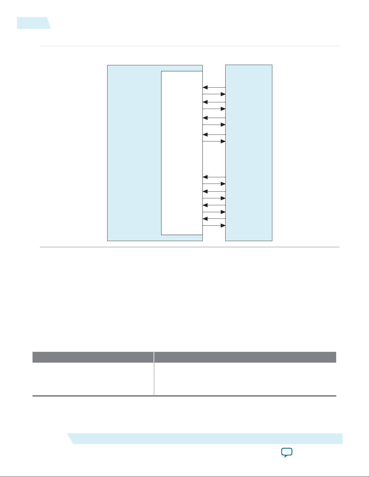
RX Mapping and TX Mapping Parameters
The HMC Controller IP core provides the RX mapping and TX mapping parameters for flexibility in
board design.
The default values of these parameters specify the correct IP core behavior when the HMC device
LxTX[<i>] output signal connects to the HMC Controller IP core hmc_lxrx[<i>] input port, and the
LxRX[<i>] input signal connects to the HMC Controller IP core hmc_lxtx[<i>] output port, for each
<i>.
However, if your design constraints prevent you from connecting these signals as expected, you can
instead modify one or both HMC Controller IP core mapping parameters to accommodate the nonstandard connection.
The Quartus II Fitter prevents you from mapping the HMC Controller IP core lanes to Arria 10
Note:
device transceiver channels out of order. Therefore, these two parameters only compensate for outof-order connections on the board between the Arria 10 transceiver pins and the HMC device
ports.
Getting Started with the HMC Controller IP Core
Send Feedback
Altera Corporation
Page 15
FPG A
HMC Controller
Hybrid Memory Cube
hmc_lxtx[0] LxRX[0]
LxTX[0]hmc_lxrx[0]
hmc_lxtx[1] LxRX[1]
LxTX[1]hmc_lxrx[1]
hmc_lxtx[2] LxRX[2]
LxTX[2]hmc_lxrx[2]
hmc_lxtx[3] LxRX[3]
LxTX[3]hmc_lxrx[3]
hmc_lxtx[F] LxRX[F]
LxTX[F]hmc_lxrx[F]
hmc_lxtx[E] LxRX[E]
LxTX[E]hmc_lxrx[E]
hmc_lxtx[D] LxRX[D]
LxTX[D]hmc_lxrx[D]
hmc_lxtx[C] LxRX[C]
LxTX[C]hmc_lxrx[C]
. . . . . . . . .
RX mapping value 0xFEDCBA9876543210
TX mapping value 0xFEDCBA9876543210
2-6
RX Mapping and TX Mapping Parameters
Figure 2-2: Default RX and TX Mapping Parameter Values
UG-01152
2015.05.04
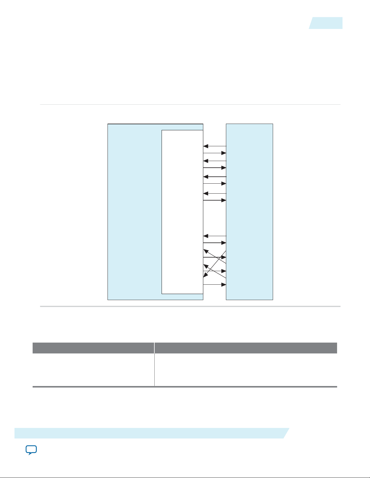
If the HMC device LxTX[<i>] output signal connects to the HMC Controller IP core hmc_lxrx[<k>]
input port, the value in bits [(4<i>+3):(4<i>)] (nibble <i>) of the RX mapping parameter is 4'h<k>.
Therefore, the default value of the RX mapping parameter is 0xFEDCBA9876543210, indicating that
LxTX[F] connects to hmc_lxrx[F], LxTX[E] connects to hmc_lxrx[E], and so on.
If the HMC device LxRX[<i>] input signal connects to the HMC Controller IP core hmc_lxtx[<k>] input
port, the value in bits [(4<i>+3):(4<i>)] (nibble <i>) of the TX mapping parameter is 4'h<k>. Therefore,
the default value of the TX mapping parameter is 0xFEDCBA9876543210, indicating that LxRX[F]
connects to hmc_lxtx[F], LxRX[E] connects to hmc_lxtx[E], and so on.
Example: Non-Default RX Mapping Parameter Value
Table 2-2: Non-Default RX Connections
HMC Device Output Signal IP Core Input Signal
LxTX[2] hmc_lxrx[0]
LxTX[1] hmc_lxrx[2]
LxTX[0] hmc_lxrx[1]
Altera Corporation
Getting Started with the HMC Controller IP Core
Send Feedback
Page 16
FPGA
HMC Controller
Hybrid Memory Cube
hmc_lxtx[0] LxRX[0]
LxTX[0]hmc_lxrx[0]
hmc_lxtx[1] LxRX[1]
LxTX[1]hmc_lxrx[1]
hmc_lxtx[2] LxRX[2]
LxTX[2]hmc_lxrx[2]
hmc_lxtx[3] LxRX[3]
LxTX[3]hmc_lxrx[3]
hmc_lxtx[F] LxRX[F]
LxTX[F]hmc_lxrx[F]
hmc_lxtx[E] LxRX[E]
LxTX[E]hmc_lxrx[E]
hmc_lxtx[D] LxRX[D]
LxTX[D]hmc_lxrx[D]
hmc_lxtx[C] LxRX[C]
LxTX[C]hmc_lxrx[C]
. . . . . . . . .
RX mapping value 0xFEDCBA9876543021
TX mapping value 0xFEDCBA9876543210
UG-01152
2015.05.04
RX Mapping and TX Mapping Parameters
Figure 2-3: Non-Default RX Mapping Parameter Value Example
If you connect the IP core hmc_lxrx[2:0] input signals according to the table, and connect all other IP
core hmc_lxrx[<i>] input ports to the corresponding HMC device LxTX[<i>] output ports, you would
set the value of the RX mapping parameter to 0xFEDCBA9876543021 to compensate for the nonstandard connection.
Note: The RX mapping parameter specifies the HMC device lane by position and the IP core lane by
value. The figure illustrates a mapping parameter value of 0xFED.......43021 and not a value of
0xFED....43102.
2-7
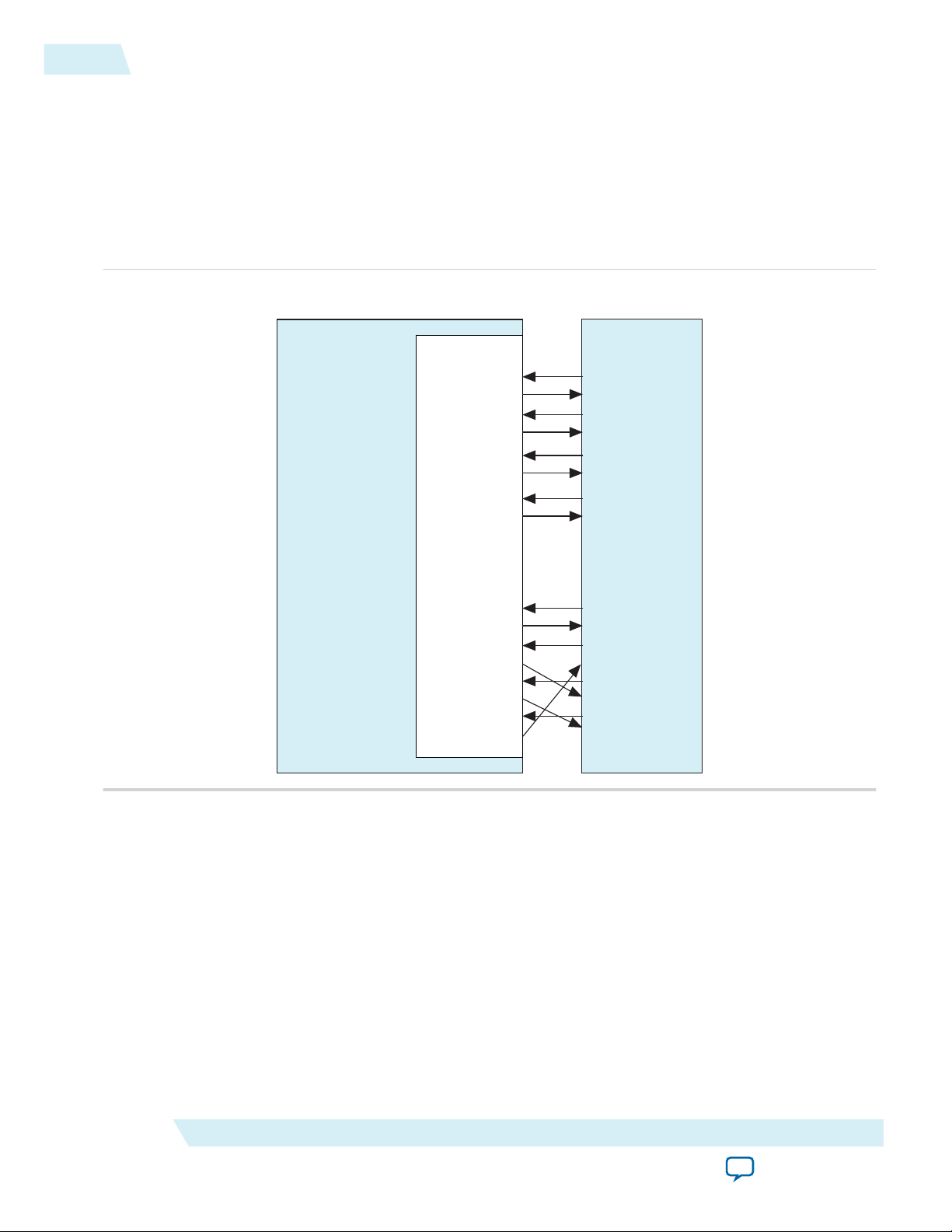
Example: Non-Default TX Mapping Parameter Value
Table 2-3: Non-Default TX Connections
HMC Device Input Signal IP Core Output Signal
LxRX[2] hmc_lxtx[0]
LxRX[1] hmc_lxtx[2]
LxRX[0] hmc_lxtx[1]
Getting Started with the HMC Controller IP Core
Send Feedback
Altera Corporation
Page 17
FPGA
HMC Controller
Hybrid Memory Cube
hmc_lxtx[0] LxRX[0]
LxTX[0]hmc_lxrx[0]
hmc_lxtx[1] LxRX[1]
LxTX[1]hmc_lxrx[1]
hmc_lxtx[2] LxRX[2]
LxTX[2]hmc_lxrx[2]
hmc_lxtx[3] LxRX[3]
LxTX[3]hmc_lxrx[3]
hmc_lxtx[F] LxRX[F]
LxTX[F]hmc_lxrx[F]
hmc_lxtx[E] LxRX[E]
LxTX[E]hmc_lxrx[E]
hmc_lxtx[D] LxRX[D]
LxTX[D]hmc_lxrx[D]
hmc_lxtx[C] LxRX[C]
LxTX[C]hmc_lxrx[C]
. . . . . . . . .
RX mapping value 0xFEDCBA9876543210
TX mapping value 0xFEDCBA9876543021
2-8
Files Generated for Altera IP Cores
Figure 2-4: Non-Default TX Mapping Parameter Value Example
If you connect the HMC Controller IP core hmc_lxtx[2:0] output signals according to the table, and
connect all other IP core hmc_lxtx[<i>] output ports to the corresponding HMC device LxRX[<i>]
input ports, you would set the value of the TX mapping parameter to 0xFEDCBA9876543021 to
compensate for the non-standard connection.
Note: The TX mapping parameter specifies the HMC device lane by position and the IP core lane by
value. The figure illustrates a mapping parameter value of 0xFED.......43021 and not a value of
0xFED....43102.
UG-01152
2015.05.04
Use caution in modifying these parameters. In loopback configurations, you must ensure the RX
mapping and TX mapping parameters specify reversed mappings. Otherwise, the IP core downstream of
the RX lane swapper appears to receive data on the wrong lanes.
Files Generated for Altera IP Cores
The Quartus II software generates multiple files during generation of your IP core variation.
Altera Corporation
Getting Started with the HMC Controller IP Core
Send Feedback
Page 18
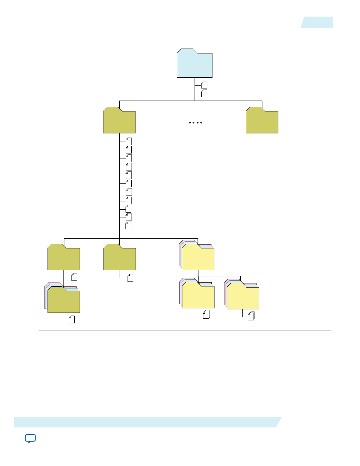
<your_ip >.cmp - VHDL component declaration file
<your_ip >.ppf - XML I/O pin information file
<your_ip >.qip - Lists IP synthesis files
<your_ip >.sip - Lists files for simulation
<your_ip >.v or .vhd
Top-level IP synthesis file
<your_ip >.v or .vhd
Top-level simulation file
<simulator_setup_scripts >
<your_ip >.qsys - System or IP integration file
<your_ip >_bb.v - Verilog HDL black box EDA synthesis file
<your_ip >_inst.v or .vhd - Sample instantiation template
<your_ip >_generation.rpt - IP generation report
<your_ip >.debuginfo - Contains post-generation information
<your_ip >.html - Connection and memor y map data
<your_ip >.bsf - Block symbol schematic
<your_ip >.spd - Combines individual simulation scripts
<your_ip >.sopcinfo - Software tool-chain integration file
<project directory>
<your_ip>
IP variation files
sim
Simulation files
synth
IP synthesis files
<EDA tool name>
Simulator scripts
<ip subcores> n
Subcore libraries
sim
Subcore
Simulation files
synth
Subcore
synthesis files
<HDL files >
<HDL files >
<your_ip> n
IP variation files
UG-01152
2015.05.04
Figure 2-5: IP Core Generated Files
Integrating Your IP Core in Your Design
2-9
Integrating Your IP Core in Your Design
To ensure the HMC Controller IP core functions correctly in hardware, you must connect additional
blocks to your IP core and assign device pins in order.
Pin Constraints
Getting Started with the HMC Controller IP Core
Send Feedback
Altera Corporation
Page 19

2-10
Required External Blocks
UG-01152
2015.05.04
When you integrate your HMC Controller IP core instance in your design, you must make appropriate
pin assignments. You can create a virtual pin to avoid making specific pin assignments for top-level
signals while you are simulating and not ready to map the design to hardware.
When you are ready to map the design to hardware, you must enforce the following constraints:
• Adjacent HMC Controller lanes must map to adjacent Altera device pins. You cannot swap the lane
order by mapping lanes to other Altera device pins. Instead, use the RX mapping and TX mapping
parameters to compensate for board design issues.
• The lanes of an HMC Controller IP core must be configured in no more than three transceiver blocks.
To enforce this constraint, you must configure IP core lanes in transceiver channels with the following
restrictions:
• Lane 0 of a full-width HMC Controller IP core must map to channel 0, 1, or 2 of a transceiver
block.
• If Lane 0 maps to channel 0, then HMC Controller Lane 1 must map to channel 1 of the same
transceiver block (transceiver block N), and Lane 15 maps to channel 3 of the transceiver block
N+2.
• If Lane 0 maps to channel 1, then HMC Controller Lane 1 must map to channel 2 of the same
transceiver block (transceiver block N), and Lane 15 maps to channel 4 of the transceiver block
N+2.
• If Lane 0 maps to channel 2, then HMC Controller Lane 1 must map to channel 3 of the same
transceiver block (transceiver block N), and Lane 15 maps to channel 5 of the transceiver block
N+2.
• Lane 0 of a half-width HMC Controller IP core can map to any channel. If it maps to any of
channels 0, 1, 2, 3, or 4, the IP core lanes are configured in two transceiver blocks.
Required External Blocks
The HMC Controller IP core requires that you define and instantiate the following additional modules:
• One or more external PLL IP cores to configure transceiver TX PLLs for all of the HMC lanes.
Although the hardware these IP cores configure might physically be part of the device transceiver, you
must instantiate them in software separately from the HMC Controller IP core. This requirement
supports the configuration of multiple Altera IP cores using the same transceiver block in the device.
• An external I2C master module in your design. Your design must include this module to initialize the
HMC device to which your IP core connects.
Altera Corporation
Getting Started with the HMC Controller IP Core
Send Feedback
Page 20
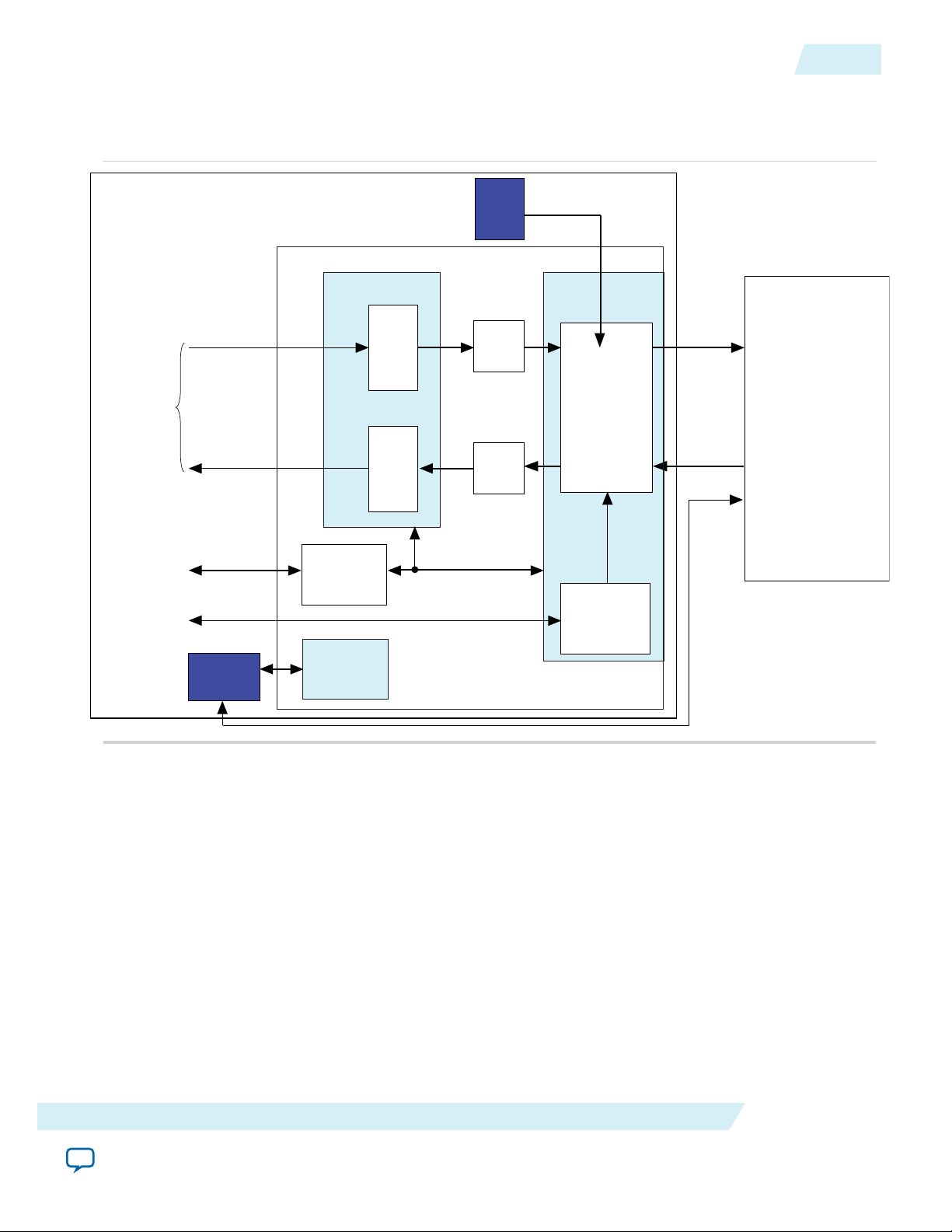
HMC Controller IP Core
FPGA
TX
FIFO
TX
RX
Control and
Status Interface
InitializationInitialization
State Machine State Machine
Arria 10
Transceiver
Reconfiguration
Interface
Avalon-MM
Application
Interface
TX Lane
Swapper
RX Lane
Swapper
Avalon-MM
I C Master
Transceiver
x8
or
x16
TX PLLs
HMC Device
2
UG-01152
2015.05.04
Adding the External PLL
Figure 2-6: Required External Blocks
The required external blocks appear darker than the other blocks in the figure. The external TX PLL IP
core configures an ATX PLL in the device transceiver or an fPLL in Transceiver mode.
2-11
Adding the External PLL
The HMC Controller IP core requires that you generate and connect external transceiver PLL IP cores.
You must generate the number of PLL IP cores required to clock the transceiver channels that are
configured as HMC Controller IP core lanes. Each ATX PLL IP core configures the transceiver PLL in the
transceiver in hardware, but you must generate the transceiver PLL IP core separately from the HMC
Getting Started with the HMC Controller IP Core
Controller IP core in software. You can also configure an fPLL in transceiver mode. If you do not generate
and connect the transceiver PLL IP core or cores, the HMC Controller IP core does not function correctly
in hardware.
You can use the IP Catalog to generate each external PLL IP core that configures a transceiver PLL on the
device. In the IP Catalog, select Arria 10 Transceiver ATX PLL or Arria 10 fPLL.
Send Feedback
Altera Corporation
Page 21

2-12
Adding the External PLL
UG-01152
2015.05.04
In the transceiver PLL parameter editor, you must follow the instructions in the Arria 10 Transceiver PHY
User Guide to configure the PLL IP core in the xN bonding configuration or in the PLL feedback
compensation bonding configuration. In addition, you must set the following parameter values:
• PLL output frequency to one half of the per-lane data rate of the IP core variation. The transceiver
performs dual edge clocking, using both the rising and falling edges of the input clock from the PLL.
Therefore, this PLL output frequency setting drives the transceiver with the correct clock for the lanes
that connect to the HMC device.
• PMA interface width to 32.
• PLL integer reference clock frequency (ATX PLL) or Desired reference clock frequency (fPLL)
depends on the bonding scheme.
• In the xN bonding scheme, Altera recommends that you specify one of 125 MHz, 156.25 MHz, or
166.67 MHz. You can theoretically specify any reference clock frequency from which the PLL can
generate the required output clock frequency. However, you must drive this TX PLL and the RX
CDR PLL (rx_cdr_refclk0 input signal to the HMC Controller IP core) and the HMC device
reference clock input signals (REFCLKP and REFCLKN) from the same clock source.
• In the PLL feedback compensation bonding scheme, you must specify the lane rate divided by 32.
In this mode, the PLL is configured to bypass the reference clock divider. Therefore, if you select
this bonding scheme, the reference clock frequency must be the lane rate divided by the PMA
width, which is 32.
Note: You must drive the external PLL reference clock input signal at the frequency you specify for
this parameter.
Table 2-4: Required PLL Reference Clock Frequency with PLL Feedback Compensation Bonding
Lane Rate Required PLL Reference Clock Frequency
10 Gbps 312.5 MHz
12.5 Gbps 390.625 MHz
The number of external PLLs you must define depends on the bonding mode you specify. In xN bonding
mode, a single PLL is sufficient to drive the channels in the configured transceiver blocks. Recall that your
HMC link TX serial lanes must be configured in order in adjacent physical transceiver channels so that
these lanes configure a maximum of three transceiver blocks. You can view I/O constraints that enforce
these requirements in the example design Quartus Settings File hmcc_example.qsf provided with the HMC
Controller IP core.
You set the bonding mode in the PLL parameter editor. In PLL Feedback Compensation mode, each PLL
output connects to the x6 network for its transceiver block through the transceiver block's Master Clock
Generation Block. In xN bonding mode, the PLL output connects directly to the x6 network for its
transceiver block and drives additional transceiver blocks through the xN clock network.
Altera Corporation
Getting Started with the HMC Controller IP Core
Send Feedback
Page 22

ATX PLL
pll_powerdown
pll_locked
pll_cal_busy
HMC Controller IP Core
Txvr Block N
Txvr Block N+1
Txvr Block N+2
pll_locked
pll_cal_busy
pll_powerdown
tx_bonding_clocks (Channel 5)
tx_bonding_clocks (Channel 4)
tx_bonding_clocks (Channel 3) (Lane 15)
tx_bonding_clocks (Channel 2) (Lane 14)
tx_bonding_clocks (Channel 1) (Lane 13)
tx_bonding_clocks (Channel 0) (Lane 12)
tx_bonding_clocks (Channel 5) (Lane 11)
tx_bonding_clocks (Channel 4) (Lane 10)
tx_bonding_clocks (Channel 3) (Lane 9)
tx_bonding_clocks (Channel 2) (Lane 8)
tx_bonding_clocks (Channel 1) (Lane 7)
tx_bonding_clocks (Channel 0) (Lane 6)
tx_bonding_clocks (Channel 5) (Lane 5)
tx_bonding_clocks (Channel 4) (Lane 4)
tx_bonding_clocks (Channel 3) (Lane 3)
tx_bonding_clocks (Channel 2) (Lane 2)
tx_bonding_clocks (Channel 1) (Lane 1)
tx_bonding_clocks (Channel 0) (Lane 0)
tx_bonding_clocks[5:0]
UG-01152
2015.05.04
Adding the External PLL
Figure 2-7: Transceiver PLL Connections Example with xN Bonding Scheme
Example connections between a full-width HMC Controller IP core and a single ATX PLL IP core in xN
bonding mode.
2-13
Getting Started with the HMC Controller IP Core
Send Feedback
Altera Corporation
Page 23

ATX PLL
ATX PLL
ATX PLL
ATX PLL
ATX PLL
ATX PLL
pll_locked
pll_powerdown
pll_powerdown
pll_powerdown
pll_locked
pll_locked
pll_cal_busy
pll_cal_busy
pll_cal_busy
HMC Controller IP Core
Txvr Block N
Txvr Block N+1
Txvr Block N+2
pll_locked
pll_cal_busy
pll_powerdown
tx_bonding_clocks (Channel 5)
tx_bonding_clocks (Channel 4)
tx_bonding_clocks (Channel 3) (Lane 15)
tx_bonding_clocks (Channel 2) (Lane 14)
tx_bonding_clocks (Channel 1) (Lane 13)
tx_bonding_clocks (Channel 0) (Lane 12)
tx_bonding_clocks (Channel 5) (Lane 11)
tx_bonding_clocks (Channel 4) (Lane 10)
tx_bonding_clocks (Channel 3) (Lane 9)
tx_bonding_clocks (Channel 2) (Lane 8)
tx_bonding_clocks (Channel 1) (Lane 7)
tx_bonding_clocks (Channel 0) (Lane 6)
tx_bonding_clocks (Channel 5) (Lane 5)
tx_bonding_clocks (Channel 4) (Lane 4)
tx_bonding_clocks (Channel 3) (Lane 3)
tx_bonding_clocks (Channel 2) (Lane 2)
tx_bonding_clocks (Channel 1) (Lane 1)
tx_bonding_clocks (Channel 0) (Lane 0)
tx_bonding_clocks[5:0]
tx_bonding_clocks[5:0]
tx_bonding_clocks[5:0]
2-14
Adding the External PLL
Figure 2-8: Transceiver PLL Connections Example with PLL Feedback Compensation Scheme
Example connections between a full-width HMC Controller IP core and one ATX PLL IP core per
transceiver block. The PLL IP cores are in PLL Feedback Compensation Mode.
UG-01152
2015.05.04
You must connect the external PLL signals and the HMC Controller IP core transceiver TX PLL interface
signals according to the following rules:
tx_bonding_clocks[5:0] input signal
for HMC lane N
pll_locked input signal Logical AND of the pll_locked output signals of the external
Altera Corporation
HMC Controller Signal Connects to TX PLL Signal
tx_bonding_clocks[5:0] output vector of PLL IP core for the
transceiver block in which lane N is configured.
In the case of xN bonding, a single PLL connects to the xN
clock network and the tx_bonding_clocks[5:0] input pins
for HMC lanes in a different transceiver block from the
configured PLL receive the clock from the xN clock network.
PLLs for all of the HMC lanes.
In the case of xN bonding, the single external PLL pll_locked
output signal connects directly to the pll_locked input pin of
the HMC Controller IP core.
Getting Started with the HMC Controller IP Core
Send Feedback
Page 24

UG-01152
2015.05.04
Adding the External I2C Master Module
HMC Controller Signal Connects to TX PLL Signal
pll_powerdown output signal pll_powerdown reset pin of the external PLLs for all of the
HMC lanes.
pll_cal_busy input signal Logical OR of the pll_cal_busy output signals of the external
PLLs for all of the HMC lanes.
In the case of xN bonding, the single external PLL pll_cal_
busy output signal connects directly to the pll_cal_busy input
pin of the HMC Controller IP core.
User logic must provide the AND and OR functions and connections.
Related Information
• External PLL Interface on page 3-4
• Signals on the Interface to the External PLLs on page 4-15
• HMC Controller IP Core Example Design on page 6-1
The HMC Controller example design provides an example of how to connect external PLLs to your
HMC Controller IP core.
• Pin Constraints on page 2-9
Describes the requirement that your IP core lanes configure a maximum of three transceiver blocks.
• Arria 10 Transceiver PHY User Guide
Information about the bonding configurations and the correspondence between PLLs and transceiver
channels, and information about how to configure an external PLL for your own design. You specify
the bonding mode in the PLL parameter editor.
2-15
Adding the External I2C Master Module
The HMC Controller IP core requires that you instantiate an external I2C master module in your design.
Your design must include this module to initialize the HMC device to which your IP core connects.
The I2C master module in your system must load the HMC device configuration registers according to
the initialization requirements of the specific HMC device in your system.
The HMC specification requires that you set the HMC device REGISTER REQUEST commands register to
the value of Init Continue after sending the commands to initialize the HMC. Therefore, the I2C master
module must set this register to indicate successful completion of the HMC device configuration register
load sequence.
Getting Started with the HMC Controller IP Core
Send Feedback
Altera Corporation
Page 25

2-16
Simulating Altera IP Cores in other EDA Tools
UG-01152
2015.05.04
In addition, the I2C master module must provide the following two signals to connect to the HMC
Controller IP core:
• An input signal that accepts requests to load the configuration registers of the HMC device. You must
connect this signal to the HMC Controller IP core i2c_load_registers output signal. If multiple
HMC Controller IP cores connect to the same HMC device, you must connect this input signal to the
AND of the individual HMC Controller IP core i2c_load_registers output signals. You must
provide the AND function.
• An output signal that indicates successful completion of the configuration register load sequence. The
I2C master must implement this signal with the following behavior:
1. Deassert this signal when coming out of reset.
2. Assert this signal after writing Init Continue to the HMC device REGISTER REQUEST commands
register.
3. Deassert this signal in response to the falling edge of the input signal described above.
You must connect this signal to the HMC Controller IP core i2c_registers_loaded input signal. If
multiple HMC Controller IP cores connect to the same HMC device, you must connect this signal to
the i2c_registers_loaded signals of all of the HMC Controller IP cores.
For information about the required register configuration sequence, you must refer to the data sheet of
the HMC device that is connected to your HMC Controller IP core. Recall that the HMC Controller IP
core operates in Response Open Loop Mode, and you must configure the HMC device to communicate
correctly with the IP core in this mode. In addition, because the IP core does not support the TGA field,
you must configure the HMC device to respond to every non-posted Write request with a Write response
packet.
Related Information
• HMC Controller IP Core Example Design on page 6-1
The HMC Controller example design provides an example I2C master module and demonstrates how
to connect it to your HMC Controller IP core.
• Interface to External I2C Master on page 3-3
• Signals on the Interface to the I2C Master on page 4-9
Describes the signals on this interface and the four-way handshaking protocol that the HMC
Controller IP core implements and that the I2C master must implement for correct IP core function‐
ality.
• HMC Specification 1.1
The Power-On and Initialization section of the HMC specification describes the initialization sequence
requirements.
Simulating Altera IP Cores in other EDA Tools
The Quartus II software supports RTL and gate-level design simulation of Altera IP cores in supported
EDA simulators. Simulation involves setting up your simulator working environment, compiling
simulation model libraries, and running your simulation.
You can use the functional simulation model and the testbench or example design available with your IP
core for simulation. When you click the Example Design button, the functional simulation model and
testbench files are generated in a location you specify. By default, if you do not modify the target location,
they are generated in a project subdirectory. This directory includes scripts to compile and run the
Altera Corporation
Getting Started with the HMC Controller IP Core
Send Feedback
Page 26

Post-fit timing
simulation netlist
Post-fit timing
simulation (3)
Post-fit functional
simulation netlist
Post-fit functional
simulation
Analysis & Synthesis
Fitter
(place-and-route)
TimeQuest Timing Analyzer
Device Programmer
Quartus II
Design Flow
Gate-Level Simulation
Post-synthesis
functional
simulation
Post-synthesis functional
simulation netlist
(Optional) Post-fit
timing simulation
RTL Simulation
Design Entry
(HDL, Qsys, DSP Builder)
Altera Simulation
Models
EDA
Netlist
Writer
UG-01152
2015.05.04
Simulating Altera IP Cores in other EDA Tools
testbench. For a complete list of models or libraries required to simulate your IP core, refer to the scripts
generated with the testbench.
Figure 2-9: Simulation in Quartus II Design Flow
2-17
Note: Post-fit timing simulation is not supported for 28nm and later device architectures. Therefore, the
HMC Controller IP core does not support post-fit timing simulation.
Altera IP supports a variety of simulation models, including simulation-specific IP functional simulation
models and encrypted RTL models, and plain text RTL models. These are all cycle-accurate models. The
models support fast functional simulation of your IP core instance using industry-standard VHDL or
Verilog HDL simulators. For some cores, only the plain text RTL model is generated, and you can
simulate that model.
Note:
Use the simulation models only for simulation and not for synthesis or any other purposes. Using
these models for synthesis creates a nonfunctional design.
If you use an HMC BFM to simulate your HMC Controller IP core, ensure that you set the BFM
parameters to match the features of your HMC Controller IP core and design. For example, confirm that
you set the BFM memory size (2G or 4G) to match the address space that you expect your design to
access, and that you set the BFM to communicate correctly with the HMC Controller IP core in Response
Open Loop Mode. You must also set the BFM to send Write response packets for non-posted Write
transactions received, because the HMC Controller IP core does not support the TGA field.
Related Information
Simulating Altera Designs
Getting Started with the HMC Controller IP Core
Send Feedback
Altera Corporation
Page 27

2-18
Understanding the Testbench
Understanding the Testbench
Altera provides an example design with the HMC Controller IP core. The example design is available both
for simulation of your IP core and for compilation. The example design in simulation functions as the
HMC Controller IP core testbench.
If you click Example Design in the HMC Controller parameter editor, the Quartus II software generates a
demonstration testbench. The parameter editor prompts you for the desired location of the testbench.
To simulate the testbench, you must provide your own HMC bus functional model (BFM). The example
design simulates with the Micron Hybrid Memory Cube BFM. The testbench does not include an I2C
master module, because the Micron HMC BFM does not support configuration by an I2C module.
In simulation, the testbench controls a TX PLL and the data path interfaces to perform the following
sequence of actions:
1. Configures the HMC BFM with the HMC Controller IP core data rate and channel width, in Response
Open Loop Mode.
2. Establishes the link between the BFM and the IP core.
3. Directs the IP core to write four packets of data to the BFM.
4. Directs the IP core to read back the data from the BFM.
5. Checks that the read data matches the write data.
6. If the data matches, displays TEST_PASSED.
UG-01152
2015.05.04
Related Information
HMC Controller IP Core Example Design on page 6-1
The HMC Controller IP core example design provides a testbench for simulation. The example design
also supports compilation and configuration.
Generating and Running the Testbench
To simulate the testbench, you must provide your own HMC bus functional model (BFM). The testbench
is designed for use with the HMC BFM r27742.
To generate and simulate the HMC Controller IP core example design, follow these steps:
1. In the Quartus II software IP Catalog, select the HMC Controller IP core and click Add.
2. When prompted you must specify the IP core instance name. If you specify the name <my_ip>, the
software generates the file <my_ip>.qsys.
3. In the HMC Controller parameter editor, set the parameter values to configure the IP core variation
you wish to simulate.
4. Click the Example Design button and specify the desired location of the testbench.
5. On the command line, change directory to <example design directory>/example_design/sim.
6. Create the simulation scripts by typing make scripts. The scripts are designed and tested for use with
the HMC BFM r27742.
Note:
7. Execute the simulation script in the directory by typing the relevant command line.
You can type make clean to delete all simulation-generated files. make clean does not delete
the scripts that the make scripts command creates.
Altera Corporation
Getting Started with the HMC Controller IP Core
Send Feedback
Page 28

UG-01152
2015.05.04
Generating and Running the Testbench
Note: You must specify <HMC BFM directory> as an absolute path.
Simulator License Command Line
2-19
Mentor Graphics
make vsim HMC_MODEL=<HMC BFM directory>
QuestaSim
Synopsys VCS make vcs HMC_MODEL=<HMC BFM directory>
Cadence NCSIM make ncsim HMC_MODEL=<HMC BFM directory>
The following options are available to view the simulation results:
• When you run the testbench in any of the three supported simulators, the script executes the testbench
sequence and logs the simulator activity in <example design directory>/example_design/sim/
<simulator>.log. <simulator> is "vsim", "ncsim", or "vcs".
• When you run the testbench in any of the three supported simulators, the script generates a waveform
file. You can run the command make <simulator>_gui to load the waveform in the simulator-specific
waveform viewer.
• The make vcs_gui command opens the Synopsys Discovery Visual Environment and displays the
file <example design directory>/example_design/sim/hmcc_wf.vpd.
• The make ncsim_gui command opens the Cadence SimVision Waveform window and displays the
waveform in the <example design directory>/example_design/sim/cadence/hmcc_wf.shm directory.
• The make vsim_gui command opens the Mentor Graphics ModelSim waveform viewer and
displays the file <example design directory>/example_design/sim/mentor/hmcc_wf.wlf.
Getting Started with the HMC Controller IP Core
Send Feedback
Altera Corporation
Page 29

2015.05.04
HMC Controller IP Core
TX
FIFO
Link
Master
Link
Slave
256- or 512-Bit Data
256- or 512-Bit Data
Control and
Status Block
InitializationInitialization
State Machine State Machine
Arria 10
Transceiver
Reconfiguration
Block
Avalon-MM
TX Lane
Swapper
RX Lane
Swapper
Avalon-MM
Interface to PLL IP Cores
to HMC device
from HMC device
Transceiver
x8
or
x16
Application
Interfaces
Control and Status
Interface
Arria 10 Transceiver
Dynamic Reconfiguration
Interface
Interface to
I C Master
2
www.altera.com
101 Innovation Drive, San Jose, CA 95134
Functional Description
3
UG-01152
Subscribe
Send Feedback
The Altera HMC Controller MegaCore IP core enables easy access to external HMC devices.
High Level Block Diagram
Figure 3-1: HMC Controller IP Core Block Diagram
©
2015 Altera Corporation. All rights reserved. ALTERA, ARRIA, CYCLONE, ENPIRION, MAX, MEGACORE, NIOS, QUARTUS and STRATIX words and logos are
trademarks of Altera Corporation and registered in the U.S. Patent and Trademark Office and in other countries. All other words and logos identified as
trademarks or service marks are the property of their respective holders as described at www.altera.com/common/legal.html. Altera warrants performance
of its semiconductor products to current specifications in accordance with Altera's standard warranty, but reserves the right to make changes to any
products and services at any time without notice. Altera assumes no responsibility or liability arising out of the application or use of any information,
product, or service described herein except as expressly agreed to in writing by Altera. Altera customers are advised to obtain the latest version of device
specifications before relying on any published information and before placing orders for products or services.
ISO
9001:2008
Registered
Page 30

3-2
Interfaces Overview
The HMC Controller IP core includes the following components:
• Two data paths, an HMC TX path and an HMC RX path. Each path includes a link layer module, a
lane swapper, and high-speed transceivers on the HMC link.
• An initialization state machine.
• A register control block.
• An Arria 10 Native PHY dynamic reconfiguration block.
The TX lane swapper remaps the HMC TX lanes to transceiver channels according to the TX mapping
parameter. The RX lane swapper remaps the HMC RX lanes from transceiver channels according to the
RX mapping parameter.
Interfaces Overview
The Altera HMC Controller IP core supports multiple external interfaces.
Application Interfaces
The data path request and response interfaces, also called the application request interface and the
application response interface, provide a 256-bit or 512-bit data bus and dedicated signals for the applica‐
tion to provide HMC request packet field values and to read HMC response packet field values.
UG-01152
2015.05.04
The interfaces support HMC Read and HMC Write requests with specific payload sizes.
Table 3-1: Application Data Width and Supported Payloads Depend on IP Core Variation
IP Core Variation Full-width Half-width
Memory Interface to HMC Device 16-lane link 8-lane link
Client Data Interface Width 512 bit 256 bit
READ and WRITE Transaction Payload Support
(Bytes)
Related Information
16, 32, 64, 128 16, 32, 48, 64, 80, 96, 112,
128
Application Interface Signals on page 4-1
HMC Interface
The HMC interface connects to the external HMC device, and complies with the HMC specification. The
interface provides a single 8-lane or 16-lane link, configured in an Altera device in 8 or 16 adjacent
transceiver channels.
The HMC Controller IP core operates in Response Open Loop Mode.
Related Information
• HMC Interface Signals on page 4-8
The HMC Controller IP core's HMC interface connects to the external HMC device's link interface and
main reset signal.
• HMC Controller IP Core Supported HMC Transaction Types on page 1-3
Altera Corporation
Functional Description
Send Feedback
Page 31

UG-01152
2015.05.04
Interface to External I2C Master
The HMC Controller IP core requires that you instantiate an external I2C master module in your design.
This external I2C master module must coordinate link initialization on the link between the HMC and the
HMC Controller. The I2C master coordinates with the HMC Controller internal initialization state
machine and programs configuration registers in the HMC device to which your IP core connects.
Separating the HMC Controller IP core from the I2C master module provides design flexibility. Because
the IP core does not include the I2C master module, you can instantiate a single I2C master to control link
initialization for multiple HMC Controller IP cores. A single I2C master module can also control other
I2C slaves.
Related Information
• Adding the External I2C Master Module on page 2-15
Information about how to connect the HMC Controller IP core to the external I2C master module.
• Signals on the Interface to the I2C Master on page 4-9
Describes the signals on this interface and the four-way handshaking protocol that the HMC
Controller IP core implements and that the I2C master must implement for correct IP core function‐
ality.
Control and Status Register Interface
Interface to External I2C Master
3-3
The control and status register interface provides access to the HMC Controller IP core internal control
and status registers. This interface does not provide access to the transceiver registers.
The control and status interface complies with the Avalon Memory-Mapped (Avalon-MM) specification
defined in the Avalon Interface Specifications.
The control and status interface provides a 32-bit wide data bus for register content. All HMC Controller
control and status registers are 32 bits wide and all register accesses through the control and status
interface read or write the full 32 bits of register content.
Related Information
• Control and Status Interface Signals on page 4-10
• HMC Controller IP Core Register Map on page 5-1
• Avalon Interface Specifications
Status and Debug Interface
The status and debug interface provides signals to communicate successful link initalization and to
support debugging of your HMC system.
Related Information
Status and Debug Signals on page 4-11
Transceiver Control Interfaces
The HMC Controller IP core supports the following transceiver control interfaces:
External PLL Interface on page 3-4
Transceiver Reconfiguration Interface on page 3-4
Functional Description
Send Feedback
Altera Corporation
Page 32

3-4
External PLL Interface
External PLL Interface
The HMC Controller IP core requires that you generate one or more external transceiver PLL IP cores
and connect one of the PLL IP cores to each HMC Controller IP core lane.
If you do not generate and connect the transceiver PLL IP cores, the HMC Controller IP core does not
function correctly in hardware.
Related Information
• Adding the External PLL on page 2-11
Describes how to generate an external transceiver PLL IP core, including parameter requirements.
• Signals on the Interface to the External PLLs on page 4-15
• HMC Controller IP Core Example Design on page 6-1
The HMC Controller example design provides an example of how to connect external PLLs to your
HMC Controller IP core.
• Arria 10 Transceiver PHY User Guide
Information about the Arria 10 transceiver PLLs and clock network.
Transceiver Reconfiguration Interface
The transceiver reconfiguration interface provides access to the registers in the embedded Native PHY IP
core. This interface provides direct access to the hard PCS registers on the device.
UG-01152
2015.05.04
The transceiver reconfiguration interface complies with the Avalon Memory-Mapped (Avalon-MM)
specification defined in the Avalon Interface Specifications.
Related Information
• Transceiver Reconfiguration Signals on page 4-13
• Avalon Interface Specifications
Defines the Avalon Memory-Mapped (Avalon-MM) specification.
• Arria 10 Transceiver PHY User Guide
Information about the Arria 10 transceiver reconfiguration interface.
• Arria 10 Transceiver Registers
Detailed information about the Arria 10 transceiver registers.
Clocking and Reset Structure
The HMC Controller IP core has a single core clock domain and multiple transceiver-related clock
domains.
Your design must derive the external transceiver TX PLL reference clock, the RX CDR reference clock,
and the REFCLKP and REFCLKN input signals of the external HMC device from the same clock reference
source. This requirement ensures a 0 PPM difference between the receive and transmit clocks, as required
by the HMC specification.
Altera Corporation
Functional Description
Send Feedback
Page 33

TX PLL
pll_refclk0
HMC Controller IP Core
Transceiver
x16
core_clk
reconfig_clk
tx_bonding_clocks[95:90]
tx_bonding_clocks[5:0]
tx_clkout[CHANNELS-1:0]
reconfig_clk
[0]
rx_cdr_refclk0
.
.
.
UG-01152
2015.05.04
Figure 3-2: HMC Controller IP Core Clocking Diagram
Related Information
Clock and Reset Signals on page 4-12
Lists the clock and reset signals and the relationships between them.
Initialization
3-5
Initialization
When you assert the active low rst_n signal, you trigger initialization of the HMC Controller IP core, the
HMC device, and the HMC link that connects them. To ensure the correct sequence, you must connect
the HMC Controller IP core, the I2C master module, and the HMC device correctly.
The following signals control HMC Controller IP core, HMC link, and HMC device initialization:
• rst_n: Active low HMC Controller IP core input signal that triggers IP core initialization
• hmc_p_rst_n: HMC Controller IP core output signal. You should connect this signal to the active low
HMC device P_RST_N input signal. P_RST_N triggers HMC device initialization.
• i2c_load_registers: HMC Controller IP core output signal. You should connect this signal to the
I2C master module input signal that tells the I2C master module to load the configuration registers of
the HMC device.
• i2c_registers_loaded: HMC Controller IP core input signal that indicates the I2C master module
has completed its part in the initialization of the HMC device. You should connect this signal to the
I2C master module output signal that indicates successful completion of the HMC configuration
register load sequence.
The IP core reports link initialization status in the InitializationState field of the LINK_STATUS
register at offset 0x10. The HMC device reports its own link iniitialization status in its own link interface
status registers.
Functional Description
Send Feedback
Altera Corporation
Page 34

rst_n
hmc_p_rst_n
(connects to HMC P_RST_N)
i2c_load_registers
i2c_registers_loaded
HMC Controller Status Register
(InitializationState field of
LINK_STATUS register)
Reset Start HMC Transmit Null
Transmit TSI
Wait for TRET Active
Scrambled Null
TS1 Scrambled Null Normal Traffic
Scrambled Null TS1 Scr. Null & TRET Normal Traffic
PRBS
HMC Controller IP Core TX HMC Link
(sending to HMC device)
HMC Controller IP Core RX HMC Link
(receiving from HMC device)
in Host Link Mode
High Z
0x01
Reset State
0x02
RX Clock Align
0x04
Descrambler
Sync
0x08
Non-Zero
Wait
0x10 & 0x20
TS1 Sync
& RX Lane
Deskew
0x40
Zero Wait
0x80
Active
HMC Device Link Interface Status
0x240002 - Link 0
0x250002 - Link 1
0x260002 - Link 2
0x270002 - Link 3
Notes:
1. HMC Controller IP core acquires descrambler sync. The Descrambler Sync field of the Lane Status register goes to all ones.
2. HMC Controller IP core does word and lane alignment. The Lanes Aligned bit pf the Link Status register goes to 1 and the Word Lock field of the Lane Status register goes to all ones.
(1) (2)
PRBS
3-6
M20K ECC Support
When you initialize the HMC link, recall the following HMC Controller IP core requirements:
• The HMC Controller IP core operates in Response Open Loop Mode, and you must configure the
HMC device to communicate correctly with the IP core in this mode.
• The IP core does not support the TGA field, so you must configure the HMC device to acknowledge
every non-posted Write request with a Write response packet.
Figure 3-3: HMC Link Initialization Sequence
UG-01152
2015.05.04
Altera Corporation
Related Information
• Adding the External I2C Master Module on page 2-15
Describes the I2C master module requirements and the module's connections to the HMC Controller
IP core.
• Signals on the Interface to the I2C Master on page 4-9
Describes the detailed behavior of the I2C master module during initialization.
• HMC Interface Signals on page 4-8
This interface includes the hmc_p_rst_n signal.
• Clock and Reset Signals on page 4-12
• LINK_STATUS Register on page 5-4
M20K ECC Support
If you turn on Enable M20K ECC support in your HMC Controller IP core variation, the IP core takes
advantage of the built-in device support for ECC checking in all M20K blocks configured in the IP core on
the device. The feature performs single-error correct, double-adjacent-error correct, and triple-adjacenterror detect ECC functionality in the M20K memory blocks configured in your IP core.
The HMC Controller IP core reports ECC error statistics in the registers RETRY_ECC_COUNT at offset 0x38
and RESPONSE_ECC_COUNT at offset 0x3C.
Functional Description
Send Feedback
Page 35

UG-01152
2015.05.04
Flow Control
Flow Control
3-7
This feature enhances data reliability but increases request-to-response latency and resource utilization.
Enabling this feature might reduce the maximum operating frequency (f
) and might increase the
MAX
difficulty of closing timing in full-width variations.
Related Information
Error and Retry Statistics Registers on page 5-9
Describes the RETRY_ECC_COUNT and RESPONSE_ECC_COUNT registers.
Embedded Memory Blocks in Arria 10 Devices
Information about the built-in ECC feature in Arria 10 devices.
The HMC specification describes two possible flow control schemes for host-to-HMC traffic, token based
flow control and Response Open Loop Mode.
In token-passing mode, the device sends information about its buffering capacity to the HMC link partner
during transaction layer initialization. In Response Open Loop Mode, the device does not send informa‐
tion about its buffering capacity to the HMC link partner. Instead, it only sends a request packet when it
has room to receive the response at any time.
The HMC Controller IP core operates in Response Open Loop Mode. The IP core is designed to have the
capacity to accept all response packets from the HMC device.
When user requests come in faster than the HMC Controller IP core can send them out on the HMC link,
the HMC Controller IP core backpressures the application by deasserting the dp_req_ready signal.
Error Detection and Management
The HMC specification defines error detection and recovery processes. The HMC Controller IP core
complies with these requirements, and implements the following additional features to support error
management:
• Error Response queues to support software handling without dropping Error Responses that arrive in
quick succession
• Statistics registers that count the number of packets in various error categories
Table 3-2: HMC Response Packet Field Checking
The HMC Controller checks these HMC response packet fields for error indications, and handles errors by
entering Error Abort mode to force the HMC device to retransmit the packet. In this mode, the IP core completes
transmission of any partially transmitted packet and then submits IRTRY packets, per the HMC specification. The
IP core also sets the indicated bit in the INTERRUPT_STATUS register and increments the Local Count field of the
LOCAL_ERROR_COUNT register.
Response Packet Field Error Indication INTERRUPT_STATUS Register Bit
LNG and DLN The two fields have different
CRC Incorrect CRC CRC Error
Functional Description
Send Feedback
LNG/DLN Error
values, or an invalid value
Altera Corporation
Page 36

3-8
Testing Features
Response Packet Field Error Indication INTERRUPT_STATUS Register Bit
SEQ Unexpected value SEQ Error
The HMC Controller IP core also checks the ERRSTAT field value and treats the response according to the
following rules:
• If ERRSTAT has the value of zero, this field indicates no errors or conditions. The IP core processes the
response packet as usual.
• If ERRSTAT has a non-zero value in a Read response, Write response, or MODE response packet, the IP
core processes the response as usual, but asserts the dp_rsp_error signal on the RX data path interface
when passing the response to the application.
• If ERRSTAT has a non-zero value in an Error response packet, the IP core does not forward the Error
response packet to the RX data path interface. Instead, the IP core diverts the packet's ERRSTAT and
cube ID values to the internal Error Response FIFO. The first element of the internal Error Response
FIFO is always readable in the ERROR_RESPONSE register. You can process these packets in software.
The HMC Controller IP core transmits 32 IRTRY packets in a retry sequence, and expects to receive 20
IRTRY packets from the HMC device.
Related Information
UG-01152
2015.05.04
• Interrupt Related Registers on page 5-5
Describes the INTERRUPT_STATUS interrupt bits CRC Error, SEQ Error, and LNG/DLN Error.
• Error and Retry Statistics Registers on page 5-9
Describes the Local Count field of the LOCAL_ERROR_COUNT register.
• ERROR_RESPONSE Register on page 5-5
Describes the ERROR_RESPONSE register and the Error Response queue.
Testing Features
The HMC Controller IP core supports multiple testing features.
• You can control the following testing features by writing fields in the HMC Controller IP core CONTROL
register:
• Force the HMC Controller IP core to detect an error in the input stream and send a StartRetry
request to the HMC device.
• Inject a single-bit error in the CRC of the next request packet.
• Force the Retry State Machine to exit the fatal error state.
• Force the HMC device and the IP core to reset.
• You can use the testing features that the Native PHY IP core provides. You control these features by
writing fields in the hard PCS registers. Write access to these registers is available through the
transceiver reconfiguration interface. If you turn on Enable Altera Debug Master Endpoint (ADME),
write access to these registers is also available through a JTAG master accessible from the Quartus II
System Console.
Altera Corporation
Functional Description
Send Feedback
Page 37

UG-01152
2015.05.04
Testing Features
Related Information
• Transceiver Reconfiguration Signals on page 4-13
• CONTROL Register on page 5-2
• Arria 10 Transceiver PHY User Guide
Information about configuring the Arria 10 transceiver registers through the Arria 10 transceiver
reconfiguration interface and about the ADME reconfiguration featue of the Arria 10 Native PHY IP
core.
• Arria 10 Transceiver Registers
Information about the Arria 10 transceiver registers.
3-9
Functional Description
Send Feedback
Altera Corporation
Page 38

2015.05.04
www.altera.com
101 Innovation Drive, San Jose, CA 95134
HMC Controller IP Core Signals
4
UG-01152
Subscribe
Send Feedback
The HMC Controller IP core communicates with other design components through multiple interfaces.
The IP core has the following top-level signals:
Application Interface Signals on page 4-1
HMC Interface Signals on page 4-8
The HMC Controller IP core's HMC interface connects to the external HMC device's link interface and
main reset signal.
Signals on the Interface to the I2C Master on page 4-9
Your design must include an I2C master module that drives the HMC device I2C interface for link
initialization. This interface connects to the I2C module.
Control and Status Interface Signals on page 4-10
Status and Debug Signals on page 4-11
Clock and Reset Signals on page 4-12
Transceiver Reconfiguration Signals on page 4-13
Signals on the Interface to the External PLLs on page 4-15
Application Interface Signals
The application interface supports easy access to the external HMC device by providing a simple data path
interface to specify memory read and write requests and to receive memory read and write responses. This
interface is also called the data path interface.
Related Information
Application Interfaces on page 3-2
Application Request Interface
The data path request interface, or application request interface, provides a 512-bit or 256-bit data bus
and dedicated signals for the application to provide HMC request packet field values to the HMC
Controller IP core. Full-width variations have a 512-bit data bus, and half-width variations have a 256-bit
data bus. The interface supports Write requests with payload sizes up to 128 bytes. In full-width
variations, the maximum payload size limits the interface to data bursts of 2 or fewer core_clk clock
©
2015 Altera Corporation. All rights reserved. ALTERA, ARRIA, CYCLONE, ENPIRION, MAX, MEGACORE, NIOS, QUARTUS and STRATIX words and logos are
trademarks of Altera Corporation and registered in the U.S. Patent and Trademark Office and in other countries. All other words and logos identified as
trademarks or service marks are the property of their respective holders as described at www.altera.com/common/legal.html. Altera warrants performance
of its semiconductor products to current specifications in accordance with Altera's standard warranty, but reserves the right to make changes to any
products and services at any time without notice. Altera assumes no responsibility or liability arising out of the application or use of any information,
product, or service described herein except as expressly agreed to in writing by Altera. Altera customers are advised to obtain the latest version of device
specifications before relying on any published information and before placing orders for products or services.
ISO
9001:2008
Registered
Page 39

dp_req_ready
dp_req_valid
dp_req_tag[8:0]
dp_req_cmd[5:0]
dp_req_cube[2:0]
dp_req_addr[33:0]
dp_req_data[255:0] or [511:0]
dp_req_sop
dp_req_eop
HMC Controller
IP Core
TX Client
Logic
4-2
Application Request Interface
cycles. In half-width variations, the maximum payload size limits the interface to data bursts of 4 or fewer
core_clk clock cycles. Write requests and read responses with a payload size that is not a multiple of the
bus size carry the end of the payload in the lower order bits of the data bus in the final clock cycle.
The application must provide the following routing and control information for every request it sends on
the TX data path interface:
• A well-formed HMC destination address.
• A unique 9-bit in-flight tag. This requirement does not apply to posted transaction requests. The
application can reuse a tag only after the previous transaction with that tag is completely resolved.
• A correct 3-bit cube ID.
In addition, the application must ensure that it sends a request only when it is able to receive the response
to the request as soon as that response arrives.
Figure 4-1: Application to HMC Controller IP Core
The client acts as a source and the HMC Controller acts as a sink in the transmit direction.
UG-01152
2015.05.04
Table 4-1: Signals of the Data Path Request Interface
All interface signals are synchronous with the core_clk clock.
Signal Name Direction Description
dp_req_ready
Output When the HMC Controller IP core asserts this signal, the
Altera Corporation
IP core is ready to receive data. The HMC Controller IP
core accepts data when both dp_req_ready and dp_req_
valid are asserted in the same cycle.
The IP core deasserts this signal to back-pressure the
application when it cannot currently process any
incoming requests.
The IP core does not deassert this signal between the
cycles of a multi-cycle write data transfer.
HMC Controller IP Core Signals
Send Feedback
Page 40

UG-01152
2015.05.04
Application Request Interface
Signal Name Direction Description
4-3
dp_req_valid
dp_req_tag[8:0]
Input Indicates that the transaction is valid—all input signals
have valid values. The HMC Controller IP core accepts
data on the rising edge of core_clk when both dp_req_
ready and dp_req_valid are asserted.
The application must maintain this signal asserted during
a multi-cycle write data transfer.
The application can send back-to-back requests by
maintaining the dp_req_valid signal asserted.
Note: The application must update the value it drives
on dp_req_tag for the new request. If the
application continues to drive the old values on
the input signals, that new request has the same
tag as the previous request.
Input The user-generated tag associated with this request. The
corresponding response returns with the identical tag.
The value of this signal is a Don't Care for posted transac‐
tion requests. Because these requests have no
corresponding response that must be identified, they do
not require meaningful tag values.
You must ensure every tag in use at any given time by a
non-posted transaction is unique. After a response
returns, the tag is available for re-use.
dp_req_cmd[5:0]
dp_req_cube[2:0]
dp_req_addr[33:0]
The application must maintain the value on this signal
during a multi-cycle write data transfer.
Input Indicates the packet command associated with this
request. Refer to Table 17 in the HMC Specification v1.1
for the command encodings.
The application must maintain the value on this signal
during a multi-cycle write data transfer.
Input The CUB ID of the cube to which the request is directed.
The application must maintain the value on this signal
during a multi-cycle write data transfer.
Input Target address in the external HMC device. Current HMC
devices ignore the four least significant bits of the address
(and assumes they have the value of 4'b0000) in all
requests the HMC Controller IP core generates, except for
the BIT WRITE request.
The application must maintain the value on this signal
during a multi-cycle write data transfer.
HMC Controller IP Core Signals
Send Feedback
Altera Corporation
Page 41

4-4
Application Response Interface
Signal Name Direction Description
UG-01152
2015.05.04
dp_req_data[511:0] (for full-
Input Write data.
width IP cores)
The application must transfer the least significant bytes of
dp_req_data[255:0] (for half-
the write payload in the first cycle.
width IP cores)
If the size of the payload is not an integer multiple of the
data bus width, then in the final data transfer cycle, the
application must transfer the remaining write payload in
the least significant bytes of dp_req_data. For example,
the application must:
• Transfer a 16-byte payload in dp_req_data[127:0].
• Transfer a 32-byte payload to a full-width or half-width
IP core in dp_req_data[255:0].
• Transfer the final (most significant) 16 bytes of a 112byte payload to a half-width IP core in dp_req_
data[127:0] in the fourth data transfer clock cycle.
During a read request, the value on this data bus does not
matter.
dp_req_sop
Input Start of packet. The application must assert this signal in
the first cycle of all transactions.
dp_req_eop Input End of packet. The application must assert this signal in
the final cycle of all transactions.
Application Response Interface
The data path response interface, or application response interface, provides a 512-bit or 256-bit data bus
and dedicated signals for the IP core to provide HMC response information to the application. Full-width
IP cores have a 512-bit data bus, and half-width IP cores have a 256-bit data bus. The interface supports
Read responses with payload sizes up to 128 bytes. In full-width variations, the maximum payload size
limits the interface to data bursts of 2 or fewer core_clk clock cycles. In half-width variations, the
maximum payload size limits the interface to data bursts of 4 or fewer core_clk clock cycles. Read
responses with a payload size that is not a multiple of the bus size carry the end of the payload in the lower
order bits of the data bus in the final clock cycle.
The HMC Controller returns the 9-bit tag from the original request with every response it sends on the
data path response interface. The application must use the tag to match each response with the
corresponding request.
You cannot back-pressure the IP core data path response interface. To ensure the application can process
every response it receives, the application must only send requests for which it has the resources to
process or buffer the response.
Altera Corporation
HMC Controller IP Core Signals
Send Feedback
Page 42

dp_rsp_valid
dp_rsp_tag[8:0]
dp_rsp_cmd[5:0]
dp_rsp_size[2:0]
dp_rsp_data[255:0] or [511:0]
dp_rsp_error
dp_rsp_sop
dp_rsp_eop
HMC Controller
IP Core
RX Client
Logic
UG-01152
2015.05.04
Figure 4-2: HMC Controller IP Core to RX Application
The HMC Controller IP core acts as a source and the client acts as a sink in the receive direction.
Table 4-2: Signals of the Data Path Response Interface
All interface signals are clocked by the core_clk clock.
Signal Name Direction Description
Application Response Interface
4-5
dp_rsp_valid
dp_rsp_tag[8:0]
dp_rsp_cmd[5:0]
Output Indicates that all of the dp_rsp_tag, dp_rsp_cmd, dp_
rsp_error, dp_rsp_sop, and dp_rsp_eop signals are
valid, and in a read response with payload, dp_rsp_data
and dp_rsp_size are valid.
The application must accept all valid transactions. You
cannot back-pressure the HMC Controller IP core data
path response interface.
The IP core maintains this signal asserted for the duration
of a multi-cycle read data transfer.
Output The tag associated with the original request to which this
is a response.
After you process this response, the tag is available for re-
use.
The IP core maintains the value of this signal for the
duration of a multi-cycle read data transfer.
Output Indicates the packet command associated with this
response. Refer to Table 25 in the HMC Specification v1.1
for the command encodings.
The IP core maintains the value of this signal for the
duration of a multi-cycle read data transfer.
HMC Controller IP Core Signals
Send Feedback
Altera Corporation
Page 43

4-6
Application Response Interface
Signal Name Direction Description
UG-01152
2015.05.04
dp_rsp_size[2:0]
Output Indicates the size of the payload associated with this
response. If the current response is a Read response,
indicates the size of the payload in dp_rsp_data.
During a response with an associated payload, the IP core
sets this signal to one of the following valid values:
• 3'b000 indicates a 16-byte payload or a Write response.
• 3'b001 indicates a 32-byte payload.
• 3'b010 indicates a 48-byte payload (half-width IP cores
only).
• 3'b011 indicates a 64-byte payload.
• 3'b100 indicates a 80-byte payload (half-width IP cores
only).
• 3'b101 indicates a 96-byte payload (half-width IP cores
only).
• 3'b110 indicates a 112-byte payload (half-width IP
cores only).
• 3'b111 indicates a 128-byte payload.
During a response with no associated payload, the value of
this signal is undefined. Responses with no associated
payload are the responses for which dp_rsp_cmd[0] has
the value of 1.
dp_rsp_data[511:0] (for full-
width IP cores)
dp_rsp_data[255:0] (for half-
width IP cores)
The IP core maintains the value of this signal for the
duration of a multi-cycle read data transfer.
Output Read response data.
During a response with no associated payload, the value of
this signal is undefined. Responses with no associated
payload are the responses for which dp_rsp_cmd[0] has
the value of 1.
If the size of the payload is not an integer multiple of the
data bus width, then in the final data transfer cycle, the IP
core transfers the remaining read payload in the least
significant bytes of dp_rsp_data. For example, the IP
core:
• Transfers a 16-byte payload in dp_rsp_data[127:0].
• Transfers a 32-byte payload (from a full-width or halfwidth IP core) in dp_rsp_data[255:0].
• Transfers the final (most significant) 16 bytes of a 112byte payload from a half-width IP core in dp_rsp_
data[127:0] in the fourth data transfer clock cycle.
Altera Corporation
HMC Controller IP Core Signals
Send Feedback
Page 44

TAG0 TAG1 TAG2 TAG3
CUBE0 CUBE1 CUBE2 CUBE3
ADDR0 ADDR1 ADDR2 ADDR3
RD16 RD128 WR16 WR128
DATA2 DATA3a DATA3b
TAG0 TAG2 TAG1 TAG3
RD_RS WR_RS RD_RS WR_RS
0x0 0x7
DATA0 DATA1a DATA1b
core_clk
dp_req_valid
dp_req_tag[8:0]
dp_req_cube[2:0]
dp_req_addr[33:0]
dp_req_cmd[5:0]
dp_req_data[511:0]
dp_req_ready
dp_rsp_valid
dp_rsp_tag[8:0]
dp_rsp_cmd[5:0]
dp_rsp_size[2:0]
dp_rsp_data[511:0]
dp_rsp_error
dp_rsp_sop
dp_rsp_eop
dp_req_sop
dp_req_eop
UG-01152
2015.05.04
HMC Controller IP Core Data Path Example
Signal Name Direction Description
4-7
dp_rsp_error
Output Indicates that the corresponding request completed with
an error and will not be retried automatically. The HMC
Controller IP core asserts this signal if it received a Read
or Write response packet from the external HMC device
with a non-zero ERRSTAT or DINV field.
dp_rsp_sop Output Start of packet. The IP core asserts this signal in the first
cycle of all response transactions.
dp_rsp_eop Output End of packet. The IP core asserts this signal in the final
cycle of all response transactions.
HMC Controller IP Core Data Path Example
Figure 4-3: Full-Width HMC Controller IP Core Application Interface Example
HMC Controller IP Core Signals
In this example, user logic sends four consecutive request packets and the full-width HMC Controller IP
core sends the corresponding response packets. The first three requests complete without error. The
fourth request completes with an error indication.
Altera Corporation
Send Feedback
Page 45

4-8
HMC Interface Signals
When the HMC Controller IP core deasserts the dp_req_ready signal, user logic maintains the current
values until a full clock cycle after the IP core reasserts dp_req_ready. User logic is required to send the
values while dp_req_ready is asserted, to ensure that the IP core captures them correctly.
The IP core asserts the dp_rsp_error signal while sending the response to the WR128 request. This signal
indicates that the WR128 request did not complete successfully. The IP core passes this information
through from the HMC device; therefore, this signal indicates that the HMC device encountered an error
while attempting to implement the request.
HMC Interface Signals
The HMC Controller IP core's HMC interface connects to the external HMC device's link interface and
main reset signal.
Table 4-3: Signals of the HMC Interface
Signal Name Direction Description
UG-01152
2015.05.04
hmc_lxrx[15:0] (for full-width
IP cores)
hmc_lxrx[7:0] (for half-width
IP cores)
hmc_lxtx[15:0] (for full-width
IP cores)
hmc_lxtx[7:0] (for half-width
IP cores)
hmc_lxrxps
hmc_lxtxps
Input
Output
Input
Output
Receiving lanes. Implements HMC specification LxRXP
and LxRXN differential pairs.
You must connect this data bus to the HMC device LxTXP
bus. The Quartus II Fitter assigns the correct pin to the
negative signal automatically.
Transmitting lanes. Implements HMC specification LxTXP
and LxTXN differential pairs.
You must connect this data bus to the HMC device LxRXP
bus. The Quartus II Fitter assigns the correct pin to the
negative signal automatically.
Link power reduction input. Implements HMC specifica‐
tion LxRXPS signal. The HMC Controller IP core does not
use this signal, but provides it to comply with the HMC
specification.
You should connect this input signal to the HMC device
LxTXPS output signal.
Link power reduction output. Implements HMC specifica‐
tion LxTXPS signal.
You must connect this input signal to the HMC device
LxRXPS output signal.
hmc_ferr_n
hmc_p_rst_n
Altera Corporation
Input
Active-low fatal error indication from the HMC device.
You must connect this signal to the HMC device FERR_N
signal.
Output Main reset signal to the HMC device.
You must connect this signal to the HMC device P_RST_N
signal.
HMC Controller IP Core Signals
Send Feedback
Page 46

UG-01152
2015.05.04
Related Information
HMC Specification 1.1
The HMC specification is available for download from the Hybrid Memory Cube Consortium web page.
Signals on the Interface to the I2C Master
Your design must include an I2C master module that drives the HMC device I2C interface for link
initialization. This interface connects to the I2C module.
The I2C module and the IP core together must implement the following four-way handshake with the two
interface signals:
1. Resetting the IP core deasserts the i2c_load_registers signal. Resetting the I2C master module
should deassert the i2c_registers_loaded signal.
2. When the IP core and the HMC are ready, the IP core asserts i2c_load_registers. In simulation, the
IP core assumes the HMC simulation model is ready instantaneously, and in hardware, the IP core
waits the required t
3. After the I2C master module detects the assertion of i2c_load_registers, it writes to the HMC
device registers to set them up for link initialization (concluding with Init Continue) and then
asserts the i2c_registers_loaded signal.
4. The HMC Controller IP core deasserts i2c_load_registers.
5. The I2C master module deasserts i2c_registers_loaded.
duration of 20 ms.
INIT
Signals on the Interface to the I2C Master
4-9
Table 4-4: Signals on the Interface to the External I2C Master Module
The IP core i2c_load_registers signal behavior conforms to the four-way handshaking protocol. For correct
HMC Controller IP core functionality, you must design the I2C master module in your design to implement
i2c_registers_loaded signal behavior that conforms to this four-way handshaking protocol.
Signal Name Direction Description
i2c_load_registers
Output
Indicates the HMC Controller IP core is ready for the
external I2C master module to load the HMC device
configuration registers, as part of the link initialization
sequence.
You must connect this signal to the I2C master module
input port that accepts requests to load the configuration
registers of the HMC device.
i2c_registers_loaded
Input
Indicates the external HMC device registers are
configured.
You must connect this signal to the output port of the I2C
master that indicates successful completion of the configu‐
ration register load sequence.
If multiple HMC Controller IP cores are connected to different links of the same HMC device, the
external I2C master must wait until all of the HMC Controller IP cores have asserted their
i2c_load_registers signal, before writing to the HMC device configuration registers. After the external
I2C master completes writing all of the HMC configuration registers, it must assert the
i2c_registers_loaded signals for all of the HMC Controller IP cores simultaneously.
HMC Controller IP Core Signals
Send Feedback
Altera Corporation
Page 47

4-10
Control and Status Interface Signals
Related Information
HMC Controller IP Core Example Design on page 6-1
The HMC Controller example design includes an I2C master module that correctly implements the fourway handshaking protocol with the HMC Controller IP core, and that implements the recommended
sequence of register writes to initialize the Micron HMC 15G SR HMC device.
Control and Status Interface Signals
The control and status register interface is an Avalon-MM interface that provides access to the HMC
Controller IP core internal control and status registers. This interface does not provide access to the
transceiver configuration registers.
The Avalon-MM interface implements a standard memory-mapped protocol. You can connect any
Avalon master—for example, an embedded processor or JTAG Avalon master—to this bus to access the
IP core control and status registers.
Table 4-5: Control and Status Interface Signals
The core_clk clocks the signals on the HMC Controller IP core control and status interface. This interface
supports only read operations and write operations with a 32-bit payload (one full register value).
Signal Name Direction Description
UG-01152
2015.05.04
csr_address[5:0]
csr_read
csr_write
csr_writedata[31:0]
csr_readdata[31:0]
csr_readdatavalid
csr_irq
Input Byte address for register reads and writes. All HMC
Controller control and status registers are 32 bits wide.
Therefore, all addresses are 4-byte aligned.
Input You must assert this signal to request a read transfer
Input You must assert this signal to request a write transfer
Input Write data
Output Read data
Output Read data is ready for use
Output Interrupt request.
The value of this signal is not associated with the current
values of other signals on this interface. The IP core asserts
this interrupt signal asynchronously as soon as an
INTERRUPT_STATUS register bit is asserted (if the relevant
INTERRUPT_ENABLE bit is set and the GLOBAL_INTERRUPT_
ENABLE register's GlobalEnable bit has the value of 1) and
maintains the signal asserted until either one of the two
relevant enable bits is reset, or the application writes the
value of 1 to all currently-asserted INTERRUPT_STATUS
register bits.
Altera Corporation
HMC Controller IP Core Signals
Send Feedback
Page 48

UG-01152
2015.05.04
Related Information
Status and Debug Signals
• Control and Status Register Interface on page 3-3
• HMC Controller IP Core Register Map on page 5-1
• Interrupt Related Registers on page 5-5
Describes the INTERRUPT_STATUS, INTERRUPT_ENABLE, and INTERRUPT_GLOBAL_ENABLE registers.
• Avalon Interface Specifications
For more information about the Avalon-MM protocol, including timing diagrams, refer to the Avalon
Memory-Mapped Interfaces chapter.
Status and Debug Signals
Table 4-6: Status and Debug Signals
The HMC Controller IP core status and debug interface provides a few extra signals to communicate successful
link initalization and to support debugging of your HMC system.
Clock Name
Direction
Description
4-11
link_init_complete Output
debug_tx_
data[511:0] (for full-
Output This data bus shows an unscrambled copy of the striped data
width IP cores)
debug_tx_
data[255:0] (for half-
width IP cores)
debug_rx_
data[511:0] (for full-
Output This data bus shows the striped and descrambled received
width IP cores)
debug_rx_
data[255:0] (for half-
width IP cores)
Related Information
Status and Debug Interface on page 3-3
The IP core asserts this signal when the link initialization
state machine is in the active state.
before it enters the TX lane swapper. The data on this bus is
striped but not scrambled.
data after processing by the RX lane swapper and the
descrambler.
HMC Controller IP Core Signals
Send Feedback
Altera Corporation
Page 49

4-12
Clock and Reset Signals
Clock and Reset Signals
Table 4-7: HMC Controller IP Core Clock and Reset Signals
The HMC Controller IP core has a single clock domain outside of the transceiver. Your design must derive the
external TX PLL reference clock, the RX CDR reference clock, and the HMC device REFCLKP and REFCLKN input
reference clock signals from the same clock reference source.
UG-01152
2015.05.04
Clock Name
rst_n Input Active low master reset signal for the HMC Controller IP
Direction
Description
core.
When asserted, the signal must remain asserted for at least
two rx_cdr_refclk0 clock cycles.
core_rst_n Output When asserted, indicates that the HMC Controller IP core is
in reset.
The IP core deasserts the core_rst_n signal only after
core_clk is stable and the transceiver is ready to transmit
data.
rx_cdr_refclk0 Input
Reference clock for the RX transceiver CDR PLL.
You must drive this clock with the frequency you specify for
the CDR reference clock parameter.
rx_cdr_refclk0 is not the reference clock for the TX PLL.
The reference clock for the TX PLL is an input to the
external TX PLL IP cores that you connect to your HMC
Controller IP core. The reference clock for the TX PLLs does
not drive the HMC Controller IP core directly.
tx_bonding_
clocks[95:0] (for
full-width IP cores)
tx_bonding_
clocks[47:0] (for
half-width IP cores)
Altera Corporation
Input
Clocks for the individual transceiver channels. The input
clock to each transceiver channel has six bits.
You must connect this input bus to a set of external
transceiver TX PLL IP cores. You must parameterize each
external TX PLL IP core to specify an output frequency that
is 1/2 the per-lane data rate. For a 10 Gbps HMC Controller
IP core lane rate, the TX PLL IP core output frequency must
be 5 GHz; for a 12.5 Gbps lane rate, the TX PLL IP core
output frequency must be 6.25 GHz.
HMC Controller IP Core Signals
Send Feedback
Page 50

UG-01152
2015.05.04
Transceiver Reconfiguration Signals
4-13
Clock Name
core_clk Output
reconfig_clk Input
reconfig_reset Input
Related Information
Direction
• Arria 10 Transceiver PHY User Guide
Information about the Arria 10 dynamic reconfiguration interface clock and reset signals. The HMC
Controller IP core reconfig_clk and reconfig_reset input signals pass directly to the Arria 10
Native PHY IP core included in the HMC Controller IP core.
Description
Master clock for the HMC Controller IP core. The
transceiver generates core_clk. The frequency of core_clk
is the lane rate divided by 32.
Lane Rate core_clk Frequency
10 Gbps 312.5 MHz
12.5 Gbps 390.625 MHz
core_clk clocks the HMC Controller IP core signals,
including the signals on the control and status interface.
Clock for the transceiver reconfiguration interface.
Reset signal for the transceiver reconfiguration interface.
Transceiver Reconfiguration Signals
Altera provides a dedicated Avalon-MM interface, called the transceiver reconfiguration interface, to
access the transceiver registers. You access the transceiver registers through this dedicated interface and
not through the IP core general purpose control and status interface.
The Avalon-MM interface implements a standard memory-mapped protocol. You can connect an Avalon
master to this bus to access the registers of the embedded Arria 10 Native PHY IP core.
Table 4-8: HMC Controller IP Core Arria 10 Transceiver Reconfiguration Interface Signals
The reconfig_clk clocks the signals on the HMC Controller IP core Arria 10 transceiver reconfiguration
interface. The reconfig_reset input signal resets the interface.
Signal Name Direction Description
reconfig_address[13:0]
(full-width IP core)
reconfig_address[12:0]
(half-width IP core)
reconfig_read
reconfig_write
Input Word address for reads and writes. This address has 14 bits
in full-width IP core variations and 13 bits in half-width IP
core variations.
Input You must assert this signal to request a read transfer.
Input You must assert this signal to request a write transfer.
HMC Controller IP Core Signals
Send Feedback
Altera Corporation
Page 51

4-14
Transceiver Reconfiguration Signals
Signal Name Direction Description
UG-01152
2015.05.04
reconfig_
writedata[31:0]
reconfig_
readdata[31:0]
Input Write data
Output Read data
The data on reconfig_readdata[31:0] is valid on the
rising edge of reconfig_clk following a clock cycle in
which reconfig_read is asserted and reconfig_
waitrequest is deasserted.
reconfig_waitrequest
Output Indicates the IP core is not ready. You must maintain the
values on the input signals while reconfig_waitrequest is
asserted. The data on reconfig_readdata[31:0] is not
valid while reconfig_waitrequest is asserted.
Related Information
• Transceiver Reconfiguration Interface on page 3-4
• Testing Features on page 3-8
• Avalon Interface Specifications
For more information about the Avalon-MM protocol, including timing diagrams, refer to the Avalon
Memory-Mapped Interfaces chapter.
• Arria 10 Transceiver PHY User Guide
Information about the Arria 10 dynamic reconfiguration interface signals and the Arria 10 Native PHY
IP core hard PCS registers that you can program through the Arria 10 transceiver reconfiguration
interface. The HMC Controller IP core transceiver reconfiguration signals pass directly to the Arria 10
Native PHY IP core included in the HMC Controller IP core.
• Arria 10 Transceiver Registers
Detailed information about the Arria 10 transceiver registers.
Altera Corporation
HMC Controller IP Core Signals
Send Feedback
Page 52

UG-01152
2015.05.04
Signals on the Interface to the External PLLs
Signals on the Interface to the External PLLs
Table 4-9: HMC Controller IP Core External PLL Interface Signals
The HMC Controller IP core requires that you generate and connect a TX PLL IP core to each HMC Controller IP
core lane that connects to the HMC device. The HMC Controller IP core external PLL interface connects to these
PLL IP core instances.
Signal Name Direction Description
4-15
tx_bonding_
clocks[95:0] (for full-
width IP cores)
tx_bonding_
clocks[47:0] (for half-
width IP cores)
pll_locked
pll_powerdown
pll_cal_busy
Input Clocks for the individual transceiver channels. The input
clock to each transceiver channel has six bits.
You must connect this input bus to a set of external
transceiver TX PLL IP cores. You must parameterize each
external TX PLL IP core to specify an output frequency that
is 1/2 the per-lane data rate. For a 10 Gbps HMC Controller
IP core lane rate, the TX PLL IP core output frequency must
be 5 GHz; for a 12.5 Gbps lane rate, the TX PLL IP core
output frequency must be 6.25 GHz.
Input PLL-locked indication from the external TX PLLs. User
logic must drive this input signal with the AND of the pll_
locked indications from the individual transceiver channels.
core_clk can stabilize only after pll_locked is asserted.
The IP core deasserts the core_rst_n signal to indicate that
core_clk has stabilized.
Output Output signal from the IP core internal reset controller. The
IP core asserts this signal to tell the external PLLs to power
down.
Input PLL-busy indication from the external TX PLLs. When
multiple TX PLLs are instantiated, user logic must drive this
input signal with the OR of the pll_cal_busy indications
from the individual transceiver channels.
Related Information
Adding the External PLL on page 2-11
Describes how to generate and connect the external transceiver PLL IP cores to your HMC Controller IP
core.
Arria 10 Transceiver PHY User Guide
Information about the Arria 10 transceiver PLLs and clock network.
HMC Controller IP Core Signals
Send Feedback
Altera Corporation
Page 53

2015.05.04
www.altera.com
101 Innovation Drive, San Jose, CA 95134
HMC Controller IP Core Register Map
5
UG-01152
Subscribe
Send Feedback
The HMC Controller IP core internal registers are 32 bits wide and are accessible to you using the control
and status interface, an Avalon-MM interface which conforms to the Avalon Interface Specifications.
All of these registers are 32 bits wide and the addresses are shown as hexadecimal values. The registers can
be accessed only on a 32-bit (4-byte) basis. The addressing for the registers therefore increments by units
of 4.
Write accesses to a Reserved or undefined location have no effect. Read accesses to a Reserved or
undefined location return an undefined result.
Table 5-1: Register Access Codes
Lists the access codes used to describe the type of register bits.
Code Description
RW Read / write
RO Read only
RW1C Read / write 1 to clear
RTC Read to clear
Table 5-2: Control and Status Register Map
Offset Register Name Location of Additional Information
0x00 Reserved
0x04 CONTROL CONTROL Register
0x08 XCVR_STATUS XCVR_STATUS Register
0x0C LANE_STATUS LANE_STATUS Register
0x10 LINK_STATUS LINK_STATUS Register
0x14 ERROR_RESPONSE_CAPTURE ERROR_RESPONSE Register
0x18, 0x1C Reserved
©
2015 Altera Corporation. All rights reserved. ALTERA, ARRIA, CYCLONE, ENPIRION, MAX, MEGACORE, NIOS, QUARTUS and STRATIX words and logos are
trademarks of Altera Corporation and registered in the U.S. Patent and Trademark Office and in other countries. All other words and logos identified as
trademarks or service marks are the property of their respective holders as described at www.altera.com/common/legal.html. Altera warrants performance
of its semiconductor products to current specifications in accordance with Altera's standard warranty, but reserves the right to make changes to any
products and services at any time without notice. Altera assumes no responsibility or liability arising out of the application or use of any information,
product, or service described herein except as expressly agreed to in writing by Altera. Altera customers are advised to obtain the latest version of device
specifications before relying on any published information and before placing orders for products or services.
ISO
9001:2008
Registered
Page 54

5-2
CONTROL Register
Offset Register Name Location of Additional Information
0x20 INTERRUPT_STATUS
UG-01152
2015.05.04
0x24 INTERRUPT_ENABLE
Interrupt Related Registers
0x28 GLOBAL_INTERRUPT_ENABLE
0x2C Reserved
0x30 LOCAL_ERROR_COUNT
0x34 REMOTE_ERROR_COUNT
Error and Retry Statistics Registers
0x38 RETRY_BUFFER_ECC_COUNT
0x3C RESPONSE_BUFFER_ECC_COUNT
CONTROL Register
Table 5-3: HMC Controller IP Core CONTROL Register at Offset 0x04
Bits Field Name Type Value
on
Reset
31:10 Reserved RO 0
9 ForceRXError WO 0x0 Writing the value of 1 to this register field forces the HMC
Controller IP core to detect an error in the input stream and send
a StartRetry request to the HMC device. This bit is self-clearing.
Description
8 CRCErrorInjectWO 0x0 Writing the value of 1 to this register field injects a single bit error
in the CRC of the next request packet. This bit is self-clearing.
7:2 Reserved RO 0x00
1 ClearFatalErrorWO 0x0 If the Retry State Machine (RSM) is in fatal error state (RetryFata‐
lError), writing the value of 1 to this register field causes the RSM
to resume normal operation.
When a RetryFatalError occurs, the RSM halts and waits for
external corrective action. Writing the value of 1 to this register
field forces the RSM to continue.
This bit is self-clearing. It clears whether or not it affects the RSM
state.
0 Reserved RO 0x00
Related Information
Testing Features on page 3-8
Altera Corporation
HMC Controller IP Core Register Map
Send Feedback
Page 55

UG-01152
2015.05.04
XCVR_STATUS Register
Table 5-4: HMC Controller IP Core XCVR_STATUS Register at Offset 0x08
Individual transceiver status in HMC link, ordered by transceiver channel.
Bits Field Name Type Value on
Reset
31:16 Reserved RO 0x0001
XCVR_STATUS Register
Description
5-3
15:8 (half-
Reserved RO 0x00
width IP
core)
7:0 (half-
CDR Lock RO 0x00
width IP
core)
Each bit indicates whether the CDR for the
corresponding transceiver channel has locked to
15:0 (fullwidth IP
CDR Lock RO 0x00
00
the received data.
core)
LANE_STATUS Register
Table 5-5: HMC Controller IP Core LANE_STATUS Register at Offset 0x0C
Individual lane status in HMC link, ordered by transceiver channel.
Bits Field Name Type Value on
Reset
31:24
(halfwidth IP
core)
Reserved RO 0x00
Description
23:16
WordLock RO 0x00
(halfwidth IP
core)
31:16
WordLock RO 0x0000
(fullwidth IP
core)
15:8
Reserved RO 0x00
(halfwidth IP
core)
HMC Controller IP Core Register Map
Send Feedback
Each bit indicates whether the corresponding
transceiver channel in the HMC link has locked to
the TS1 word boundary.
Altera Corporation
Page 56

5-4
LINK_STATUS Register
UG-01152
2015.05.04
Bits Field Name Type Value on
Reset
7:0
DescramSync RO 0x00
(halfwidth IP
core)
Each bit indicates whether the descrambler for the
corresponding transceiver channel has synchron‐
15:0
DescramSync RO 0x0000
ized to the received data.
(fullwidth IP
core)
LINK_STATUS Register
Table 5-6: HMC Controller IP Core LINK_STATUS Register at Offset 0x10
Bits Field Name Type Value
on
Reset
31:17 Reserved RO 0x0000
Description
Description
16 RXPS RO 0x0 Level of the LxRXPS input from the HMC device.
15:9 Reserved RO 0x00
8 LanesAligned RO 0x0 Indicates whether the received data is aligned across all
lanes.
7:6 Reserved RO 0x0
5:0 InitializationStateRO 0x01
Indicates the current state in link initialization. This
register field has the following valid values:
• 6'b100000: Active
• 6'b010000: Transaction Initialization (Wait for
TRET)
• 6'b001000: Word Synchronization (Transmit TS1)
• 6'b000100: Scrambler Synchronization (Transmit
NULLs)
• 6'b000010: HMC Configuration (by the external I2C
master module)
• 6'b000001: Reset
Related Information
Initialization on page 3-5
Describes the behavior of the InitializationState field during HMC Controller IP core initialization.
Altera Corporation
HMC Controller IP Core Register Map
Send Feedback
Page 57

UG-01152
2015.05.04
ERROR_RESPONSE Register
ERROR_RESPONSE Register
Table 5-7: HMC Controller IP Core ERROR_RESPONSE Register at Offset 0x14
The HMC Controller IP core stores the ERRSTAT and CUB fields of the Error responses that it receives on the HMC
link. The IP core stores these fields in an internal Error Response queue (FIFO buffer). The application can read
the relevant information for each Error Response packet from this queue by reading the ERROR_RESPONSE register.
Reading from the register advances the queue.
Read, Write, or MODE response packets the HMC Controller IP core receives with a non-zero ERRSTAT field do
not route to this queue or register. Instead they are sent to the data path response interface with dp_rsp_error
asserted.
5-5
Bits Field Name Type Value on
Reset
Description
31:17 Reserved RO 0x0000
16 Valid RO 0x0 Indicates the CUB and ERRSTAT fields in the register hold valid
values. When the Error Response queue is empty, the CUB and
ERRSTAT fields are not valid, and the Valid bit has the value of 0.
You can poll the Valid bit to determine if any Error Response
packets are waiting to be processed, or you can enable the RX
Error Response interrupt in the INTERRUPT_ENABLE register.
15:11 Reserved RO 0x00
10:8 CUB RO 0x0 The CUB ID extracted from the TAG field of the Error Response
packet.
7 Reserved RO 0x0
6:0 ERRSTAT RO 0x00 The ERRSTAT value extracted from the Error Response packet.
Related Information
HMC Specification 1.1
Information about the encoding of the ERRSTAT response packet field is available in Table 16 in the HMC
specification.
Interrupt Related Registers
THE HMC Controller IP core has three interrupt-related registers.
• INTERRUPT_STATUS: Register bits report individual interrupt source status.
• INTERRUPT_ENABLE: Register bits individually enable the corresponding interrupts in the
INTERRUPT_STATUS register to trigger assertion of the IP core csr_irq output signal, unless the
GLOBAL_INTERRUPT_ENABLE register turns off this ability.
• GLOBAL_INTERRUPT_ENABLE: Register allows you to disable all interrupt responses or to enable those
interrupt sources indicated in the INTERRUPT_ENABLE register.
HMC Controller IP Core Register Map
Send Feedback
Altera Corporation
Page 58

5-6
Interrupt Related Registers
Table 5-8: HMC Controller IP Core INTERRUPT_STATUS Register at Offset 0x20
To clear an interrupt, write the value of 1 to the interrupt bit.
UG-01152
2015.05.04
Bits Field Name Type Value on
Reset
Description
31:16Reserved RO 0x0000
15 Response Queue
Uncorrectable
ECC Error
W1C 0x0 The IP core sets this bit if it detects an uncorrectable ECC
error in the Response Queue memory. The IP core can
detect such an error only if you turn on Enable M20K ECC
support in the parameter editor.
14 Response Queue
ECC Error
W1C 0x0 The IP core sets this bit if it detects a correctable ECC error
in the Response Queue memory. If the IP core sets this bit it
also corrects the ECC error. The IP core can detect such an
error only if you turn on Enable M20K ECC support in the
parameter editor.
13 FERR_N W1C 0x0 The IP core sets this bit if the HMC device indicates a fatal
error by asserting its active-low FERR_N pin. You must
connect the IP core hmc_ferr_n input signal to the HMC
device FERR_N output signal.
12 Retry Buffer
Uncorrectable
ECC Error
W1C 0x0 The IP core sets this interrupt bit if it detects an uncorrect‐
able ECC error in the Retry Buffer memory. The IP core can
detect such an error only if you turn on Enable M20K ECC
support in the parameter editor.
11 Retry Buffer
ECC Error
W1C 0x0 The IP core sets this interrupt bit if it detects a correctable
10 Reserved RO 0x0
9 No More Tokens W1C 0x0
ECC error in the Retry Buffer memory. The IP core
automatically corrects the ECC in this case. The IP core can
detect such an error only if you turn on Enable M20K ECC
support in the parameter editor.
The IP core sets this interrupt bit if it runs out of tokens.
Tokens represent available buffer space in the HMC device.
While the IP core has no remaining tokens, it does not send
any additional requests, per token-based flow control
requirements. This situation is not an error condition, but it
may indicate a reduction in performance. However, like any
interrupt bit, it causes the IP core to assert the csr_irq
signal (assuming the global interrupt enable register bit is
set).
This bit has the value of 0 when the IP core comes out of
reset. After link initialization, the HMC device communi‐
cates its buffer capacity with a sequence of TRET packets.
After the IP core receives the first TRET packet, it begins
updating the No More Tokens register field.
Altera Corporation
HMC Controller IP Core Register Map
Send Feedback
Page 59

UG-01152
2015.05.04
Interrupt Related Registers
5-7
Bits Field Name Type Value on
Reset
8 Retry Buffer
Full
W1C 0x0 The IP core sets this interrupt bit if the Retry buffer fills.
When the Retry buffer is full, the IP core does not send any
Description
additional Read or Write requests. This situation is not an
error condition, but it may indicate a reduction in perform‐
ance.
7 Reserved RO 0x0
6 RX Error
Response
Overflow
W1C 0x0 The IP core sets this interrupt bit if too many Error
Response packets are received before they are read from the
ERROR_RESPONSE register. If overflow occurs, the IP core
drops incoming Error Response packets until space is again
available in the Error Response queue.
5 RX Error
Response
W1C 0x0 The IP core sets this interrupt bit if the IP core receives an
Error Response packet.
4 Fatal Error W1C 0x0 The IP core sets this interrupt bit if it makes three or more
successive retry attempts that are unsuccessful.
3 Remote Error W1C 0x0 The IP core sets this interrupt bit if it receives a valid IRTRY
(StartRetry) sequence, indicating the HMC device detected
an error.
2 SEQ Error W1C 0x0 The IP core sets this interrupt bit if it receives a packet with a
SEQ field value that is not a +1 increment from the SEQ field
value of the previous packet it received.
1 LNG/DLN Error W1C 0x0 The IP core sets this interrupt bit if it receives a packet with
unequal or invalid values in the LNG (packet length) and DLN
(duplicate length) fields.
0 CRC Error W1C 0x0 The IP core sets this interrupt bit to the value of 1 if it detects
an error in the CRC of a packet it receives.
Table 5-9: HMC Controller IP Core INTERRUPT_ENABLE Register at Offset 0x24
Each bit in this register enables the corresponding interrupt in the INTERRUPT_STATUS register at offset 0x20. For
each register bit:
• If the bit has the value of 0, the interrupt is disabled.
• If the bit has the value of 1, and the GlobalEnable bit of the GLOBAL_INTERRUPT_ENABLE register at offset 0x28
has the value of 1, the interrupt is enabled.
Bits Field Name Type Value on
Reset
Description
31:16Reserved RO 0x0000
15 Response Queue
Uncorrectable
ECC Error
Enable
RW 0x0 Enables Response Queue Uncorrectable ECC Error
interrupt.
HMC Controller IP Core Register Map
Send Feedback
Altera Corporation
Page 60

5-8
Interrupt Related Registers
UG-01152
2015.05.04
Bits Field Name Type Value on
Reset
14 Response Queue
ECC Error
Enable
RW 0x0 Enables Response Queue ECC Error interrupt.
13 FERR_N Enable RW 0x0 Enables FERR_N interrupt.
12 Retry Buffer
Uncorrectable
ECC Error
Enable
11 Retry Buffer
ECC Error
Enable
RW 0x0 Enables Retry Buffer Uncorrectable ECC Error
interrupt.
RW 0x0 Enables Retry Buffer ECC Error interrupt.
10 Reserved RO 0x0
9 No More Tokens
Enable
8 Retry Buffer
Full Enable
RW 0x0 Enables No More Tokens interrupt.
RW 0x0 Enables Retry Buffer Full interrupt.
7 Reserved RO 0x0
6 RX Error
Response
Overflow
Enable
RW 0x0 Enables RX Error Response Overflow interrupt.
Description
5 RX Error
Response
Enable
4 Fatal Error
Enable
3 Remote Error
Enable
2 SEQ Error
Enable
1 LNG/DLN Error
Enable
0 CRC Error
Enable
RW 0x0 Enables RX Error Response interrupt.
RW 0x0 Enables Fatal Error interrupt.
RW 0x0 Enables Remote Error interrupt.
RW 0x0 Enables SEQ Error interrupt.
RW 0x0 Enables LNG/DLN Error interrupt.
RW 0x0 Enables CRC Error interrupt.
Table 5-10: HMC Controller IP Core GLOBAL_INTERRUPT_ENABLE Register at Offset 0x28
Gates the INTERRUPT_ENABLE register.
Bits Field Name Type Value on
Reset
Description
31:1 Reserved RO 0x00000000
Altera Corporation
HMC Controller IP Core Register Map
Send Feedback
Page 61

UG-01152
2015.05.04
Error and Retry Statistics Registers
5-9
Bits Field Name Type Value on
Reset
Description
0 GlobalEnable RW 0x0 Writing the value of 0 to this register field disables all
interrupt sources from asserting the csr_irq output signal.
Writing the value of 1 to this register field allows the IP core
to assert the csr_irq output signal according to the
interrupt sources enabled in the INTERRUPT_ENABLE register
at offset 0x24. An interrupt source causes the IP core to
assert the csr_irq output signal only if the GlobalEnable
register field and the relevant INTERRUPT_ENABLE register
field both have the value of 1.
Error and Retry Statistics Registers
The HMC Controller IP core has four statistics registers. Counter fields in these registers are all of type
RC (Read to Clear).
Table 5-11: HMC Controller IP Core LOCAL_ERROR_COUNT Register at Offset 0x30
Bits Field Name TypeValue
on
Reset
Description
31:16 Reserved RO 0x0000
15:0 Local Count RC 0x0000 Count of received packets with CRC, SEQ, or length errors. The
counter saturates at 0xFFFF.
Reading this register clears the Local Count field.
Table 5-12: HMC Controller IP Core REMOTE_ERROR_COUNT Register at Offset 0x34
Bits Field Name TypeValue
on
Reset
Description
31:16 Reserved RO 0x0000
15:0 Error Count RC 0x0000 Number of times the HMC Controller IP core began the output
error recovery process and retransmitted packets. This number
indicates the number of errors detected by the external HMC
device. This counter saturates at 0xFFFF.
Reading this register clears the Error Count field.
HMC Controller IP Core Register Map
Send Feedback
Altera Corporation
Page 62

5-10
Error and Retry Statistics Registers
Table 5-13: HMC Controller IP Core RETRY_BUFFER_ECC_COUNT Register at Offset 0x38
UG-01152
2015.05.04
Bits Field Name TypeValue
on
Reset
Description
31:24 Reserved RO 0x00
23:16 Uncorrectabl
e Count
RC 0x00 Number of uncorrectable ECC errors the IP core detected in the
Retry Buffer memory. This counter saturates at 0xFF.
This field maintains the value of zero unless you turn on Enable
M20K ECC support in the parameter editor.
Reading this register clears the Uncorrectable Count field.
15:8 Reserved RO 0x00
7:0 Correctable
Count
RC 0x00 Number of correctable ECC errors the IP core detected in the
Retry Buffer memory (and corrected). This counter saturates at
0xFF.
This field maintains the value of zero unless you turn on Enable
M20K ECC support in the parameter editor.
Reading this register clears the Correctable Count field.
Table 5-14: HMC Controller IP Core RESPONSE_BUFFER_ECC_COUNT Register at Offset 0x3C
Bits Field Name Type Value
on
Reset
31:24Reserved RO 0x00
23:
Uncorrectable
16
Count
RC 0x00 Number of uncorrectable ECC errors the IP core detected in the
15:8Reserved RO 0x00
7:0 Correctable
Count
RC 0x00 Number of correctable ECC errors the IP core detected in the
Description
Response Queue memory. This counter saturates at 0xFF.
This field maintains the value of zero unless you turn on Enable
M20K ECC support in the parameter editor.
Reading this register clears the Uncorrectable Count field.
Response Queue memory (and corrected). This counter saturates at
0xFF.
This field maintains the value of zero unless you turn on Enable
M20K ECC support in the parameter editor.
Reading this register clears the Correctable Count field.
Altera Corporation
HMC Controller IP Core Register Map
Send Feedback
Page 63

UG-01152
2015.05.04
Related Information
M20K ECC Support on page 3-6
Error and Retry Statistics Registers
5-11
HMC Controller IP Core Register Map
Send Feedback
Altera Corporation
Page 64

2015.05.04
www.altera.com
101 Innovation Drive, San Jose, CA 95134
HMC Controller IP Core Example Design
6
UG-01152
Subscribe
Send Feedback
Altera provides a compilation-ready example design with the HMC Controller IP core. This example
design targets the Arria 10 GX FPGA Development Kit with an HMC mezannine card connected through
the FMC connectors.
You can use the design as an example for correct connection of your IP core to your design, or as a starter
design you can customize for your own design requirements. The example design includes an I2C master
module, one external transceiver PLL IP core, and logic to generate and check transactions. The example
design assumes a Micron HMC 15G-SR HMC device, which is a four-link device, on the mezannine card.
©
2015 Altera Corporation. All rights reserved. ALTERA, ARRIA, CYCLONE, ENPIRION, MAX, MEGACORE, NIOS, QUARTUS and STRATIX words and logos are
trademarks of Altera Corporation and registered in the U.S. Patent and Trademark Office and in other countries. All other words and logos identified as
trademarks or service marks are the property of their respective holders as described at www.altera.com/common/legal.html. Altera warrants performance
of its semiconductor products to current specifications in accordance with Altera's standard warranty, but reserves the right to make changes to any
products and services at any time without notice. Altera assumes no responsibility or liability arising out of the application or use of any information,
product, or service described herein except as expressly agreed to in writing by Altera. Altera customers are advised to obtain the latest version of device
specifications before relying on any published information and before placing orders for products or services.
ISO
9001:2008
Registered
Page 65

HMC Controller IP Core
TX
FIFO
TX
MAC
RX
MAC
Control and
Status Interface
InitializationInitialization
State Machine State Machine
Arria 10
Transceiver
Reconfiguration
Interface
Avalon-MM
TX Lane
Swapper
RX Lane
Swapper
Avalon-MM
I C Master
Transceiver
x16
Data Path
Request
Generator
and
Response
Monitor
Test
Controller
TX PLLs
HMC Device
LEDs
Arria 10 Device
Board
2
Clocks & Reset
6-2
HMC Controller IP Core Example Design
Figure 6-1: High Level Block Diagram for the HMC Controller IP Core Example Design
The example design configures a single ATX PLL in xN bonding mode and connects it to the HMC
Controller IP core.
UG-01152
2015.05.04
Altera Corporation
The example design is provided as a Quartus II project. The example design targets the
10AX115S3F45I2SGES Arria 10 device in an Arria 10 GX FPGA Development Kit, with an HMC
mezannine card connected through the FMC connectors. To use a different device or development kit,
you must modify the project.
To set up, compile the example design, configure the example design on the device, and run the hardware
testbench on the design, follow these steps:
1. In the Quartus II software IP Catalog, under Memory Interfaces and Controllers, select Hybrid
Memory Cube Controller and click Add.
2. When prompted you must specify the IP core instance name. If you specify the name <my_ip>, the
software generates the file <my_ip>.qsys.
3. When prompted you must specify the Arria 10 device name. The example design is tested with the
10AX115S3F45I2SGES device and compiles correctly for all Arria 10 devices with the same size,
configuration, and pinout.
4. In the HMC Controller parameter editor, set the parameter values to configure your IP core variation.
5. Click the Example Design button and specify the desired location of the example design. The Quartus
II software creates an example design that includes a copy of the HMC Controller IP core.
6. Optionally, click Finish and then Yes or No to close the HMC Controller parameter editor.
7. Click File > Open Project.
HMC Controller IP Core Example Design
Send Feedback
Page 66

UG-01152
2015.05.04
HMC Controller IP Core Example Design
6-3
8. Change directory to <example design directory>/example_design/par.
9. Select hmcc_example.qpf.
10.Click Processing > Start Compilation. The project compiles and generates a SRAM Object File, hmcc_
example.sof, in the output_files folder.
11.Prepare the Arria 10 FPGA Development Kit board.
Note: Ensure that power is turned off before you change any settings.
• Add shunts to the J8 jumper to select 1.5V as the V
• Add shunts to the J11 jumper to select 1.8V as the V
setting for FMC connector B.
CCIO
setting for FMC connector A.
CCIO
12.Prepare the HMC mezzannine card.
• Set DIP switch SW1 to indicate cube ID 0:
Switch Function Setting
1 CUB[0] Open
2 CUB[1] Open
3 CUB[2] Open
4 — Don't Care
• Set DIP switch SW2 to specify clock settings:
Switch Function Setting
1 CLK1_FSEL0 Open (125 MHz)
2 CLK1_FSEL1 Open (125 MHz)
3 CLK1_SEL Open (Crystal)
4 — Don't Care
13.Use the Quartus II Programmer to configure the device on the Arria 10 FPGA Development Kit board.
After successful configuration, LED D7 on the board should display a red heartbeat (pulsing).
14.On the board, press user-defined push button PB0 (board reference S3 or schematic signal USER_PB0)
to start the testbench.
The following LEDs on the board indicate testbench results:
LED Color Meaning When Lit
D10 Red Test failed
D9 Green Test passed
D8 Green Link initialization completed
Related Information
• All Development Kits web page
For information about the Altera development kit that the example designs targets.
• Volume 3 of the Quartus II Handbook
For information about programming an Altera device, refer to the "Quartus II Programmer" chapter.
HMC Controller IP Core Example Design
Send Feedback
Altera Corporation
Page 67

2015.05.04
www.altera.com
101 Innovation Drive, San Jose, CA 95134
Additional Information
A
UG-01152
Subscribe
Send Feedback
HMC Controller IP Core User Guide Revision History
Table A-1: Document Revision History
Summarizes the new features and changes in the user guide for the HMC Controller IP core.
Date ACDS Version Changes
2015.05.04 15.0 Initial release.
How to Contact Altera
Table A-2: How to Contact Altera
To locate the most up-to-date information about Altera products, refer to this table. You can also contact your
local Altera sales office or sales representative.
Contact Contact Method Address
Technical support Website www.altera.com/support
Website www.altera.com/training
Technical training
Email custrain@altera.com
Product literature Website www.altera.com/literature
Nontechnical support: general Email nacomp@altera.com
Nontechnical support: software
Email authorization@altera.com
licensing
Related Information
• www.altera.com/support
©
2015 Altera Corporation. All rights reserved. ALTERA, ARRIA, CYCLONE, ENPIRION, MAX, MEGACORE, NIOS, QUARTUS and STRATIX words and logos are
trademarks of Altera Corporation and registered in the U.S. Patent and Trademark Office and in other countries. All other words and logos identified as
trademarks or service marks are the property of their respective holders as described at www.altera.com/common/legal.html. Altera warrants performance
of its semiconductor products to current specifications in accordance with Altera's standard warranty, but reserves the right to make changes to any
products and services at any time without notice. Altera assumes no responsibility or liability arising out of the application or use of any information,
product, or service described herein except as expressly agreed to in writing by Altera. Altera customers are advised to obtain the latest version of device
specifications before relying on any published information and before placing orders for products or services.
ISO
9001:2008
Registered
Page 68

A-2
Typographic Conventions
• www.altera.com/training
• custrain@altera.com
• www.altera.com/literature
• nacomp@altera.com
• authorization@altera.com
Typographic Conventions
Table A-3: Typographic Conventions
Lists the typographic conventions this document uses.
Visual Cue Meaning
Bold Type with Initial Capital Letters Indicate command names, dialog box titles, dialog
box options, and other GUI labels. For example,
Save As dialog box. For GUI elements, capitaliza‐
tion matches the GUI.
bold type Indicates directory names, project names, disk drive
names, file names, file name extensions, software
utility names, and GUI labels. For example, \
qdesigns directory, D: drive, and chiptrip.gdf file.
UG-01152
2015.05.04
Italic Type with Initial Capital Letters Indicate document titles. For example, Stratix V
Design Guidelines.
italic type Indicates variables. For example, n + 1.
Variable names are enclosed in angle brackets (< >).
For example, <file name> and <project name> . pof
file.
Initial Capital Letters Indicate keyboard keys and menu names. For
example, the Delete key and the Options menu.
“Subheading Title” Quotation marks indicate references to sections in a
document and titles of Quartus II Help topics. For
example, “Typographic Conventions.”
Altera Corporation
Additional Information
Send Feedback
Page 69

UG-01152
2015.05.04
Typographic Conventions
Visual Cue Meaning
A-3
Courier type
Indicates signal, port, register, bit, block, and
primitive names. For example, data1, tdi, and
input. The suffix n denotes an active-low signal.
For example, resetn.
Indicates command line commands and anything
that must be typed exactly as it appears. For
example, c:\qdesigns\tutorial\chiptrip.gdf.
Also indicates sections of an actual file, such as a
Report File, references to parts of files (for example,
the AHDL keyword SUBDESIGN), and logic function
names (for example, TRI).
1., 2., 3., and a., b., c., and so on Numbered steps indicate a list of items when the
sequence of the items is important, such as the steps
listed in a procedure.
• Bullets indicate a list of items when the sequence of
the items is not important.
The Subscribe button links to the Email Subscription Management Center page of the Altera website,
where you can sign up to receive update notifications for Altera documents.
The Feedback icon allows you to submit feedback to Altera about the document. Methods for collecting
feedback vary as appropriate for each document.
Related Information
Email Subscription Management Center
Additional Information
Send Feedback
Altera Corporation
 Loading...