

Page 1

Arria 10 Avalon-ST Interface for PCIe
Solutions
User Guide
Last updated for Altera Complete Design Suite: 15.0
Subscribe
Send Feedback
UG-01145_avst
2015.05.04
101 Innovation Drive
San Jose, CA 95134
www.altera.com
Page 2

TOC-2
Getting Started with the Arria 10 Hard IP for PCI Express with the Avalon-ST Interface
Contents
Datasheet............................................................................................................. 1-1
Arria 10 Avalon-ST Interface for PCIe Datasheet...................................................................................1-1
Arria 10 Features .............................................................................................................................1-2
Release Information ....................................................................................................................................1-6
Device Family Support ...............................................................................................................................1-7
Configurations .............................................................................................................................................1-7
Arria 10 Avalon-ST Example Designs...................................................................................................... 1-9
Debug Features ..........................................................................................................................................1-10
IP Core Verification ..................................................................................................................................1-11
Compatibility Testing Environment ..........................................................................................1-11
Performance and Resource Utilization ..................................................................................................1-11
Recommended Speed Grades ..................................................................................................................1-11
Steps in Creating a Design for PCI Express........................................................................................... 1-11
Getting Started with the Arria 10 Hard IP for PCI Express ..............................2-1
Qsys Design Flow.........................................................................................................................................2-2
Generating the Testbench ..............................................................................................................2-3
Simulating the Example Design ....................................................................................................2-3
Generating Quartus II Synthesis Files...........................................................................................2-4
Understanding the Files Generated...............................................................................................2-4
Understanding Simulation Log File Generation......................................................................... 2-4
Understanding Physical Placement of the PCIe IP Core .......................................................... 2-5
Adding Virtual Pin Assignment to the Quartus II Settings File (.qsf)..................................... 2-5
Compiling the Design in the Qsys Design Flow .........................................................................2-5
Modifying the Example Design .....................................................................................................2-7
Using the IP Catalog To Generate Your Arria 10 Hard IP for PCI Express as a Separate
Component..................................................................................................................................2-8
Files Generated for Altera IP Cores...............................................................................................2-9
Getting Started with the Configuration Space Bypass Mode Qsys Example
Design ............................................................................................................. 3-1
Copying the Configuration Space Bypass Mode Example Design .......................................................3-2
Generating the Qsys System ......................................................................................................................3-3
Generating Quartus II Synthesis Files...........................................................................................3-4
Understanding the Generated Files ..............................................................................................3-4
Understanding Simulation Log File Generation......................................................................... 3-5
Simulating the Example Design ................................................................................................................3-5
Timing for Configuration Read to Function 0 for the 256-Bit Avalon-ST Interface ............3-6
Timing for Configuration Write to Function 0 for the 256-Bit Avalon-ST Interface ...........3-8
Timing for Memory Write and Read of Function 1 256-Bit Avalon-ST Interface ................3-9
Partial Transcript for Configuration Space Bypass Simulation ..............................................3-11
Altera Corporation
Page 3

Getting Started with the Arria 10 Hard IP for PCI Express with the Avalon-ST Interface
TOC-3
Parameter Settings.............................................................................................. 4-1
System Settings ............................................................................................................................................4-1
Base Address Register (BAR) and Expansion ROM Settings ............................................................... 4-5
Base and Limit Registers for Root Ports .................................................................................................. 4-7
Device Identification Registers ..................................................................................................................4-7
PCI Express and PCI Capabilities Parameters ........................................................................................4-8
Device Capabilities ..........................................................................................................................4-9
Error Reporting .............................................................................................................................4-10
Link Capabilities ........................................................................................................................... 4-11
MSI and MSI-X Capabilities ........................................................................................................4-12
Slot Capabilities .............................................................................................................................4-13
Power Management ......................................................................................................................4-14
Vendor Specific Extended Capability (VSEC).......................................................................................4-15
PHY Characteristics ................................................................................................................................. 4-15
Physical Layout of Hard IP In Arria 10 Devices.................................................5-1
Channel and Pin Placement for the Gen1, Gen2, and Gen3 Data Rates..............................................5-4
Channel Placement and fPLL Usage for the Gen1 and Gen2 Data Rates............................................5-5
Channel Placement and fPLL and ATX PLL Usage for the Gen3 Data Rate...................................... 5-7
Interfaces and Signal Descriptions .................................................................... 6-1
Avalon-ST RX Interface .............................................................................................................................6-2
Avalon-ST RX Component Specific Signals ................................................................................6-4
Data Alignment and Timing for the 64-Bit Avalon-ST RX Interface ......................................6-6
Data Alignment and Timing for the 128-Bit Avalon-ST RX Interface ................................. 6-11
Data Alignment and Timing for 256-Bit Avalon-ST RX Interface ........................................6-15
Tradeoffs to Consider when Enabling Multiple Packets per Cycle ....................................... 6-15
Avalon-ST TX Interface ...........................................................................................................................6-16
Avalon-ST Packets to PCI Express TLPs ...................................................................................6-22
Data Alignment and Timing for the 64-Bit Avalon-ST TX Interface ................................... 6-22
Data Alignment and Timing for the 128-Bit Avalon-ST TX Interface ................................. 6-25
Data Alignment and Timing for the 256-Bit Avalon-ST TX Interface ................................. 6-28
Root Port Mode Configuration Requests ..................................................................................6-31
Clock Signals ..............................................................................................................................................6-31
Reset, Status, and Link Training Signals.................................................................................................6-31
ECRC Forwarding .....................................................................................................................................6-36
Error Signals .............................................................................................................................................. 6-36
Interrupts for Endpoints ..........................................................................................................................6-37
Interrupts for Root Ports ......................................................................................................................... 6-38
Completion Side Band Signals ................................................................................................................6-38
Parity Signals ............................................................................................................................................. 6-41
LMI Signals ................................................................................................................................................6-42
Transaction Layer Configuration Space Signals ...................................................................................6-44
Configuration Space Register Access Timing ...........................................................................6-47
Configuration Space Register Access .........................................................................................6-47
Altera Corporation
Page 4

TOC-4
Getting Started with the Arria 10 Hard IP for PCI Express with the Avalon-ST Interface
Hard IP Reconfiguration Interface .........................................................................................................6-52
Power Management Signals .................................................................................................................... 6-54
Physical Layer Interface Signals ..............................................................................................................6-57
Serial Data Signals .........................................................................................................................6-57
PIPE Interface Signals .................................................................................................................. 6-57
Test Signals .................................................................................................................................... 6-62
Registers...............................................................................................................7-1
Correspondence between Configuration Space Registers and the PCIe Specification .....................7-1
Type 0 Configuration Space Registers ..................................................................................................... 7-5
PCI Express Capability Structures.............................................................................................................7-5
Altera-Defined VSEC Registers................................................................................................................. 7-8
CvP Registers................................................................................................................................................7-9
Uncorrectable Internal Error Mask Register ........................................................................................ 7-12
Uncorrectable Internal Error Status Register ....................................................................................... 7-13
Correctable Internal Error Mask Register .............................................................................................7-14
Correctable Internal Error Status Register ............................................................................................7-14
Arria 10 Reset and Clocks................................................................................... 8-1
Reset Sequence for Hard IP for PCI Express IP Core and Application Layer ....................................8-2
Clocks ........................................................................................................................................................... 8-4
Clock Domains ................................................................................................................................8-4
Clock Summary ...............................................................................................................................8-6
Interrupts.............................................................................................................9-1
Interrupts for Endpoints.............................................................................................................................9-1
MSI Interrupts .................................................................................................................................9-1
MSI-X ............................................................................................................................................... 9-4
Implementing MSI-X Interrupts................................................................................................... 9-4
Legacy Interrupts ............................................................................................................................ 9-6
Interrupts for Root Ports ........................................................................................................................... 9-7
Error Handling ................................................................................................. 10-1
Physical Layer Errors ................................................................................................................................10-2
Data Link Layer Errors .............................................................................................................................10-2
Transaction Layer Errors .........................................................................................................................10-3
Error Reporting and Data Poisoning .....................................................................................................10-6
Uncorrectable and Correctable Error Status Bits .................................................................................10-7
IP Core Architecture......................................................................................... 11-1
Top-Level Interfaces .................................................................................................................................11-3
Avalon-ST Interface ......................................................................................................................11-3
Clocks and Reset ........................................................................................................................... 11-4
Local Management Interface (LMI Interface) .......................................................................... 11-4
Hard IP Reconfiguration ............................................................................................................. 11-4
Altera Corporation
Page 5

Getting Started with the Arria 10 Hard IP for PCI Express with the Avalon-ST Interface
Interrupts ....................................................................................................................................... 11-4
PIPE ................................................................................................................................................ 11-4
Transaction Layer ..................................................................................................................................... 11-5
Configuration Space .....................................................................................................................11-6
Error Checking and Handling in Configuration Space Bypass Mode ...................................11-7
Protocol Extensions Supported .................................................................................................11-10
Data Link Layer .......................................................................................................................................11-10
Physical Layer ..........................................................................................................................................11-12
TOC-5
Transaction Layer Protocol (TLP) Details........................................................12-1
Supported Message Types ........................................................................................................................12-1
INTX Messages ..............................................................................................................................12-1
Power Management Messages .................................................................................................... 12-2
Error Signaling Messages .............................................................................................................12-3
Locked Transaction Message ...................................................................................................... 12-4
Slot Power Limit Message ............................................................................................................12-4
Vendor-Defined Messages ...........................................................................................................12-4
Hot Plug Messages ........................................................................................................................12-5
Transaction Layer Routing Rules ........................................................................................................... 12-6
Receive Buffer Reordering .......................................................................................................................12-7
Using Relaxed Ordering ...............................................................................................................12-9
Throughput Optimization................................................................................ 13-1
Throughput of Posted Writes ................................................................................................................. 13-3
Throughput of Non-Posted Reads ......................................................................................................... 13-3
Design Implementation.................................................................................... 14-1
Making Pin Assignments to Assign I/O Standard to Serial Data Pins ..............................................14-1
Recommended Reset Sequence to Avoid Link Training Issues ......................................................... 14-1
SDC Timing Constraints.......................................................................................................................... 14-2
Optional Features..............................................................................................15-1
Configuration via Protocol (CvP) .......................................................................................................... 15-1
ECRC ..........................................................................................................................................................15-2
ECRC on the RX Path .................................................................................................................. 15-2
ECRC on the TX Path .................................................................................................................. 15-3
Hard IP Reconfiguration ..................................................................................16-1
Testbench and Design Example ....................................................................... 17-1
Endpoint Testbench ................................................................................................................................. 17-2
Root Port Testbench .................................................................................................................................17-3
Chaining DMA Design Examples .......................................................................................................... 17-4
BAR/Address Map ........................................................................................................................17-8
Altera Corporation
Page 6

TOC-6
Getting Started with the Arria 10 Hard IP for PCI Express with the Avalon-ST Interface
Chaining DMA Control and Status Registers ...........................................................................17-9
Chaining DMA Descriptor Tables ........................................................................................... 17-12
Test Driver Module ................................................................................................................................ 17-15
DMA Write Cycles ................................................................................................................................. 17-16
DMA Read Cycles ...................................................................................................................................17-18
Root Port Design Example .................................................................................................................... 17-20
Root Port BFM ........................................................................................................................................17-22
BFM Memory Map .....................................................................................................................17-24
Configuration Space Bus and Device Numbering ................................................................. 17-24
Configuration of Root Port and Endpoint ..............................................................................17-24
Issuing Read and Write Transactions to the Application Layer .......................................... 17-29
BFM Procedures and Functions ........................................................................................................... 17-30
ebfm_barwr Procedure .............................................................................................................. 17-30
ebfm_barwr_imm Procedure ....................................................................................................17-31
ebfm_barrd_wait Procedure ..................................................................................................... 17-32
ebfm_barrd_nowt Procedure ....................................................................................................17-33
ebfm_cfgwr_imm_wait Procedure ...........................................................................................17-34
ebfm_cfgwr_imm_nowt Procedure ......................................................................................... 17-34
ebfm_cfgrd_wait Procedure ......................................................................................................17-35
ebfm_cfgrd_nowt Procedure .....................................................................................................17-36
BFM Configuration Procedures................................................................................................ 17-37
BFM Shared Memory Access Procedures ............................................................................... 17-39
BFM Log and Message Procedures .......................................................................................... 17-42
Verilog HDL Formatting Functions ........................................................................................ 17-46
Procedures and Functions Specific to the Chaining DMA Design Example......................17-50
Setting Up Simulation.............................................................................................................................17-57
Changing Between Serial and PIPE Simulation ..................................................................... 17-57
Using the PIPE Interface for Gen1 and Gen2 Variants .........................................................17-57
Viewing the Important PIPE Interface Signals........................................................................17-57
Disabling the Scrambler for Gen1 and Gen2 Simulations ....................................................17-57
Disabling 8B/10B Encoding and Decoding for Gen1 and Gen2 Simulations.....................17-58
Debugging .........................................................................................................18-1
Frequently Asked Questions.............................................................................. A-1
Lane Initialization and Reversal ........................................................................B-1
Additional Information......................................................................................C-1
Altera Corporation
Simulation Fails To Progress Beyond Polling.Active State..................................................................18-1
Hardware Bring-Up Issues ......................................................................................................................18-1
Link Training .............................................................................................................................................18-2
Debugging Link Failure in L0 Due To Deassertion of tx_st_ready .......................................18-2
Use Third-Party PCIe Analyzer ..............................................................................................................18-5
BIOS Enumeration Issues ........................................................................................................................18-5
Page 7

Getting Started with the Arria 10 Hard IP for PCI Express with the Avalon-ST Interface
TOC-7
Revision History for the Avalon-ST Interface.........................................................................................C-1
How to Contact Altera............................................................................................................................... C-6
Typographic Conventions......................................................................................................................... C-7
Altera Corporation
Page 8
2015.05.04
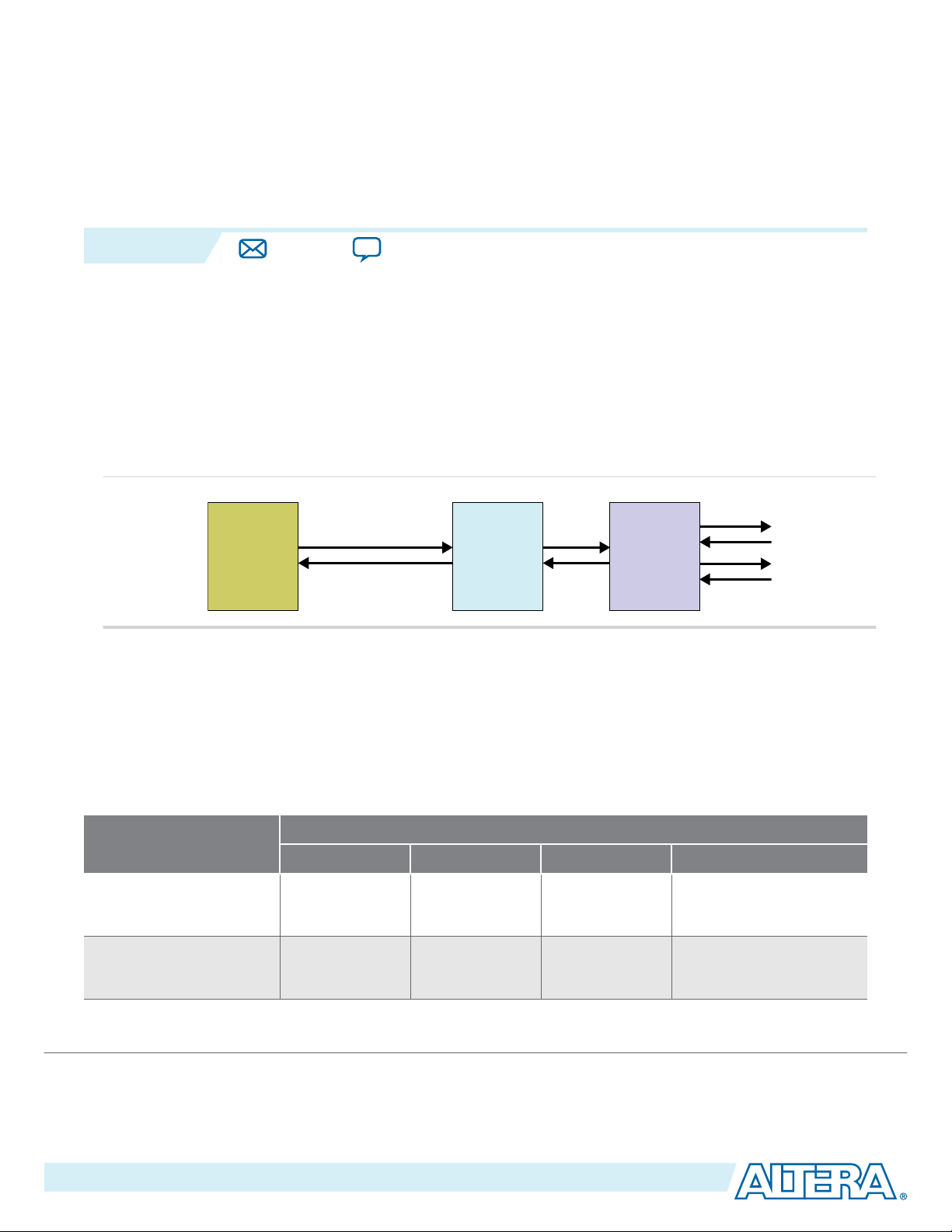
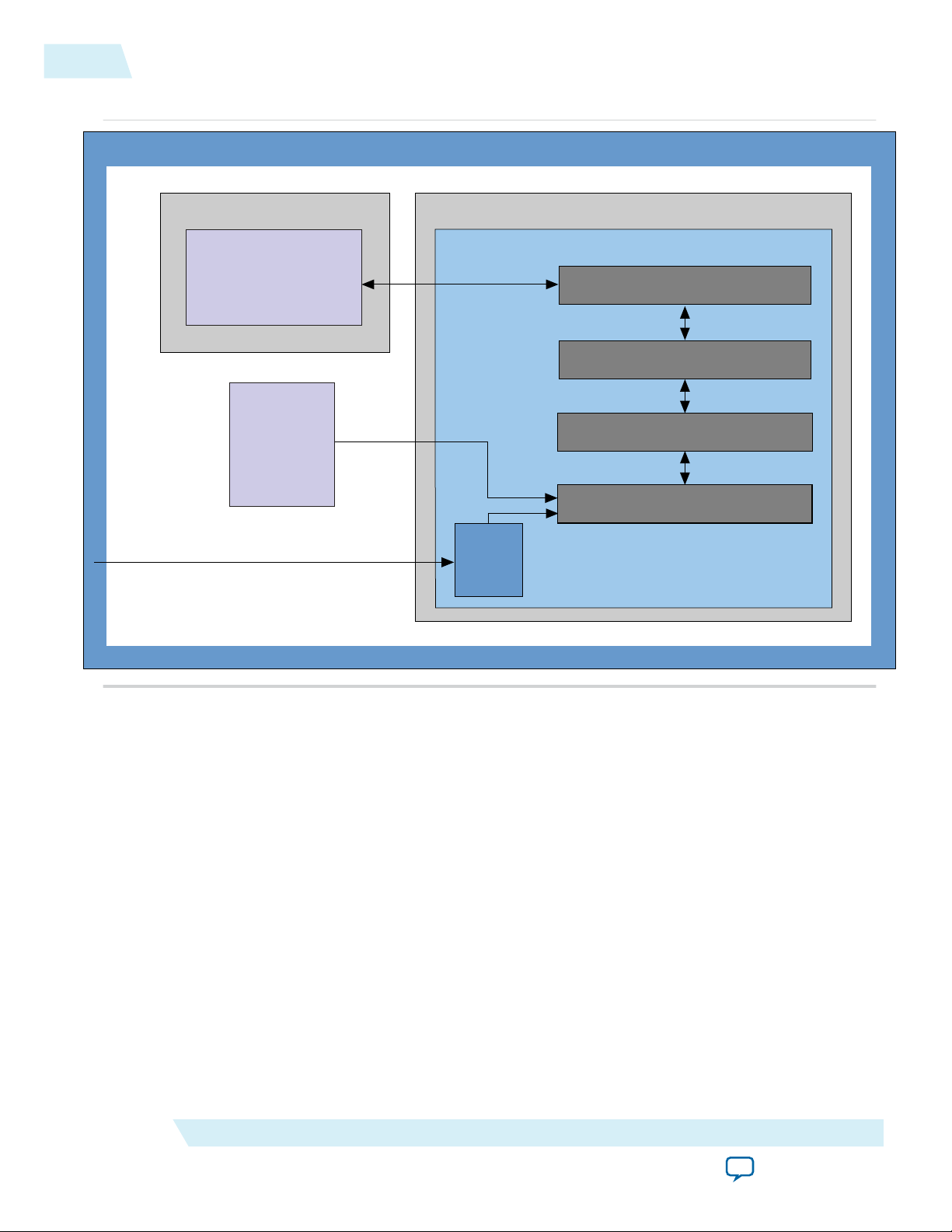
Application
Layer
(User Logic)
Avalon-ST
Interface
PCIe Hard IP
Block
PIPE
Interface
PHY IP Core
for PCIe
(PCS/PMA)
Serial Data
Transmission
www.altera.com
101 Innovation Drive, San Jose, CA 95134
Datasheet
1
UG-01145_avst
Subscribe
Send Feedback
Arria 10 Avalon-ST Interface for PCIe Datasheet
®
Altera® Arria® 10 FPGAs include a configurable, hardened protocol stack for PCI Express
compliant with PCI Express Base Specification 3.0. The Hard IP for PCI Express using the Avalon
Streaming (Avalon-ST) interface is the most flexible variant. However, this variant requires a thorough
understanding of the PCIe
®
Protocol.
Figure 1-1: Arria 10 PCIe Variant with Avalon-ST Interface
Table 1-1: PCI Express Data Throughput
The following table shows the aggregate bandwidth of a PCI Express link for Gen1, Gen2, and Gen3 for 1, 2, 4,
and 8 lanes. This table provides bandwidths for a single transmit (TX) or receive (RX) channel. The numbers
double for duplex operation. The protocol specifies 2.5 giga-transfers per second for Gen1, 5.0 giga-transfers per
second for Gen2, and 8.0 giga-transfers per second for Gen3. Gen1 and Gen2 use 8B/10B encoding which
introduces a 20% overhead. In contrast, Gen3 uses 128b/130b encoding which reduces the data throughput lost to
encoding to less than 1%.
that is
®
PCI Express Gen1
(2.5 Gbps)
PCI Express Gen2
(5.0 Gbps)
©
2015 Altera Corporation. All rights reserved. ALTERA, ARRIA, CYCLONE, ENPIRION, MAX, MEGACORE, NIOS, QUARTUS and STRATIX words and logos are
trademarks of Altera Corporation and registered in the U.S. Patent and Trademark Office and in other countries. All other words and logos identified as
trademarks or service marks are the property of their respective holders as described at www.altera.com/common/legal.html. Altera warrants performance
of its semiconductor products to current specifications in accordance with Altera's standard warranty, but reserves the right to make changes to any
products and services at any time without notice. Altera assumes no responsibility or liability arising out of the application or use of any information,
product, or service described herein except as expressly agreed to in writing by Altera. Altera customers are advised to obtain the latest version of device
specifications before relying on any published information and before placing orders for products or services.
Link Width
×1 ×2 ×4 ×8
2 4 8 16
4 8 16 32
ISO
9001:2008
Registered
Page 9

1-2
Arria 10 Features
UG-01145_avst
2015.05.04
Link Width
×1 ×2 ×4 ×8
PCI Express Gen3
(8.0 Gbps)
Refer to the AN 456: PCI Express High Performance Reference Design for more information about
calculating bandwidth for the hard IP implementation of PCI Express in many Altera FPGAs, including
the Arria 10 Hard IP for PCI Express IP core.
Devices
Related Information
• PCI Express Base Specification 3.0
• AN 456: PCI Express High Performance Reference Design
• Creating a System with Qsys
Arria 10 Features
New features in the Quartus® II 15.0 software release:
• Added Enable Altera Debug Master Endpoint (ADME) parameter to support optional Native PHY
register programming with the Altera System Console.
The Arria 10 Hard IP for PCI Express supports the following features:
• Complete protocol stack including the Transaction, Data Link, and Physical Layers implemented as
hard IP.
• Support for ×1, ×2, ×4, and ×8 configurations with Gen1, Gen2, or Gen3 lane rates for Root Ports and
Endpoints.
• Dedicated 16 KByte receive buffer.
• Optional support for Configuration via Protocol (CvP) using the PCIe link allowing the I/O and core
bitstreams to be stored separately.
• Qsys example designs demonstrating parameterization, design modules, and connectivity.
• Extended credit allocation settings to better optimize the RX buffer space based on application type.
• Support for multiple packets per cycle with the 256-bit Avalon-ST interface.
• Optional end-to-end cyclic redundancy code (ECRC) generation and checking and advanced error
reporting (AER) for high reliability applications.
• Easy to use:
7.87 15.75 31.51 63
Altera Corporation
• Flexible configuration.
• Substantial on-chip resource savings and guaranteed timing closure.
• No license requirement.
• Example designs to get started.
Datasheet
Send Feedback
Page 10

UG-01145_avst
2015.05.04
Table 1-2: Feature Comparison for all Hard IP for PCI Express IP Cores
The table compares the features of the four Hard IP for PCI Express IP Cores.
Arria 10 Features
1-3
Feature Avalon-ST Interface Avalon-MM
Interface
Avalon-MM DMA Avalon-ST Interface with SR-
IP Core License Free Free Free Free
Native
Supported Supported Supported Supported
Endpoint
Legacy
Endpoint
(1)
Supported Not Supported Not Supported Not Supported
Root port Supported Supported Not Supported Not Supported
Gen1 ×1, ×2, ×4, ×8 ×1, ×2, ×4, ×8 Not Supported
Gen2 ×1, ×2, ×4, ×8 ×1, ×2, ×4, ×8 ×4, ×8
Gen3 ×1, ×2, ×4, ×8 ×1, ×2, ×4 ×2, ×4, ×8
64-bit Applica‐
Supported Supported Not supported Not supported
×8
×4, ×8
×2, ×4, ×8
tion Layer
interface
IOV
128-bit
Supported Supported Supported Supported
Application
Layer interface
256-bit
Supported Not Supported Supported Supported
Application
Layer interface
Maximum
payload size
Number of tags
128, 256, 512,
1024, 2048 bytes
256 8 16 256
supported for
non-posted
requests
(1)
Not recommended for new designs.
128, 256 bytes 128, 256 bytes 128, 256 bytes
Datasheet
Altera Corporation
Send Feedback
Page 11

1-4
Arria 10 Features
UG-01145_avst
2015.05.04
Feature Avalon-ST Interface Avalon-MM
Interface
Automatically
Not supported Supported Supported Not supported
handle out-oforder
completions
(transparent to
the Application
Layer)
Automatically
Not supported Supported Supported Not Supported
handle requests
that cross 4
KByte address
boundary
(transparent to
the Application
Layer)
Polarity
Supported Supported Supported Supported
Inversion of
PIPE interface
signals
Avalon-MM DMA Avalon-ST Interface with SR-
IOV
Number of MSI
requests
1, 2, 4, 8, 16, or 32 1, 2, 4, 8, 16, or 32 1, 2, 4, 8, 16, or 32 1, 2, 4, 8, 16, or 32 (for
Physical Functions)
MSI-X Supported Supported Supported Supported
Legacy
Supported Supported Supported Supported
interrupts
Expansion
Supported Not supported Not supported Not supported
ROM
Table 1-3: TLP Support Comparison for all Hard IP for PCI Express IP Cores
The table compares the TLP types that the four Hard IP for PCI Express IP Cores can transmit. Each entry
indicates whether this TLP type is supported (for transmit) by endpoints (EP), Root Ports (RP), or both (EP/RP).
Transaction Layer
Packet type (TLP)
(transmit support)
Memory Read
Avalon-ST Interface Avalon-MM
Interface
Avalon-MM DMA Avalon-ST Interface with SR-
EP/RP EP/RP EP EP
IOV
Request (Mrd)
Altera Corporation
Datasheet
Send Feedback
Page 12

UG-01145_avst
2015.05.04
Arria 10 Features
1-5
Transaction Layer
Packet type (TLP)
(transmit support)
Memory Read
Lock Request
(MRdLk)
Memory Write
Request (MWr)
I/O Read
Request (IORd)
I/O Write
Request (IOWr)
Config Type 0
Read Request
(CfgRd0)
Config Type 0
Write Request
(CfgWr0)
Config Type 1
Read Request
(CfgRd1)
Avalon-ST Interface Avalon-MM
Interface
Avalon-MM DMA Avalon-ST Interface with SR-
EP/RP EP EP
EP/RP EP/RP EP EP
EP/RP EP/RP EP
EP/RP EP/RP EP
RP RP EP
RP RP EP
RP RP EP
IOV
Config Type 1
Write Request
(CfgWr1)
Message
Request (Msg)
Message
Request with
Data (MsgD)
Completion
(Cpl)
Completion
with Data
(CplD)
CompletionLocked (CplLk)
Completion
Lock with Data
(CplDLk)
RP RP EP
EP/RP EP/RP EP
EP/RP EP/RP EP
EP/RP EP/RP EP EP
EP/RP EP EP
EP/RP EP
EP/RP EP
Datasheet
Altera Corporation
Send Feedback
Page 13

1-6
Release Information
UG-01145_avst
2015.05.04
Transaction Layer
Packet type (TLP)
(transmit support)
Fetch and Add
Avalon-ST Interface Avalon-MM
EP
AtomicOp
Request
(FetchAdd)
The Arria 10 Avalon-ST Interface for PCIe Solutions User Guide explains how to use this IP core and not
the PCI Express protocol. Although there is inevitable overlap between these two purposes, use this
document only in conjunction with an understanding of the PCI Express Base Specification.
Note: This release provides separate user guides for the different variants. The Related Information
provides links to all versions.
Related Information
• Arria 10 Avalon-MM Interface for PCIe Solutions User Guide
• Arria 10 Avalon-MM DMA Interface for PCIe Solutions User Guide
• Arria 10 Avalon-ST with SR-IOV PCIe Solutions User Guide
Release Information
Interface
Avalon-MM DMA Avalon-ST Interface with SR-
IOV
Table 1-4: Hard IP for PCI Express Release Information
Item Description
Version 15.0
Release Date May 2015
Ordering Codes No ordering code is required
Product IDs There are no encrypted files for the Arria 10 Hard
IP for PCI Express. The Product ID and Vendor ID
Vendor ID
are not required because this IP core does not
require a license.
Altera Corporation
Datasheet
Send Feedback
Page 14

UG-01145_avst
2015.05.04
Device Family Support
Table 1-5: Device Family Support
Device Family Support
Device Family Support
1-7
Arria 10
Preliminary. The IP core is verified with prelimi‐
nary timing models for this device family. The IP
core meets all functional requirements, but might
still be undergoing timing analysis for the device
family. It can be used in production designs with
caution.
Other device families Refer to the Altera's PCI Express IP Solutions web
page for support information on other device
families.
Related Information
• Altera's PCI Express IP Solutions web page
Configurations
The Arria 10 Hard IP for PCI Express includes a full hard IP implementation of the PCI Express stack
including the following layers:
• Physical (PHY), including:
• Physical Media Attachment (PMA)
• Physical Coding Sublayer (PCS)
• Media Access Control (MAC)
• Data Link Layer (DL)
• Transaction Layer (TL)
Datasheet
The Hard IP supports all memory, I/O, configuration, and message transactions. It is optimized for Altera
devices. The Application Layer interface is also optimized to achieve maximum effective throughput. You
can customize the Hard IP to meet your design requirements.
Altera Corporation
Send Feedback
Page 15
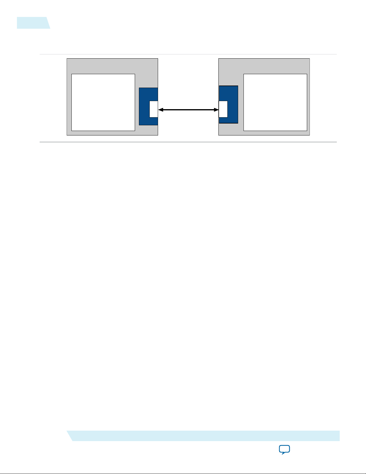
Altera FPGA
User Application
Logic
PCIe
Hard IP
RP
PCIe
Hard IP
EP
User Application
Logic
PCI Express Link
Altera FPGA
1-8
Configurations
Figure 1-2: PCI Express Application with a Single Root Port and Endpoint
The following figure shows a PCI Express link between two Arria 10 FPGAs.
Figure 1-3: PCI Express Application Using Configuration via Protocol
The Arria 10 design below includes the following components:
• A Root Port that connects directly to a second FPGA that includes an Endpoint.
• Two Endpoints that connect to a PCIe switch.
• A host CPU that implements CvP using the PCI Express link connects through the switch. For more
information about configuration over a PCI Express link, refer to Configuration via Protocol (CvP)
on page 15-1.
UG-01145_avst
2015.05.04
Altera Corporation
Datasheet
Send Feedback
Page 16
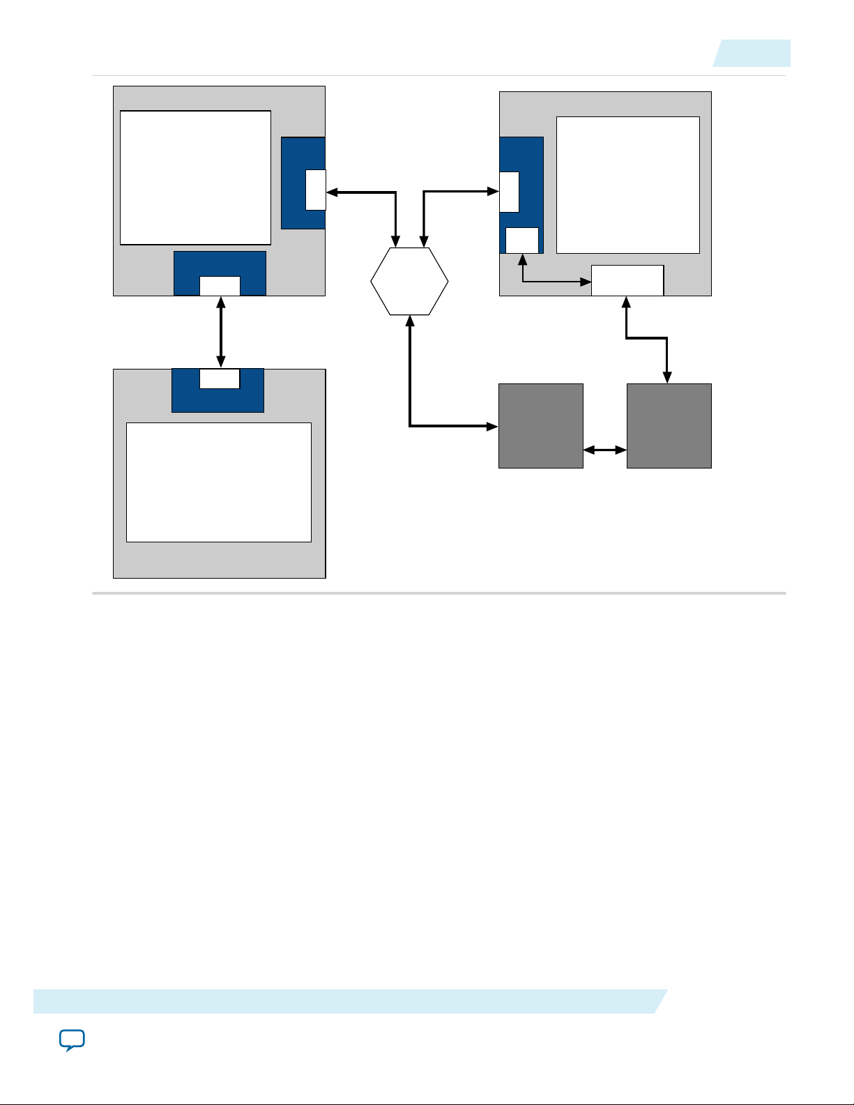
PCIe Link
PCIe Hard IP
RP
Switch
PCIe
Hard IP
RP
User Application
Logic
PCIe Hard IP
EP
PCIe Link
PCIe Link
User Application
Logic
Altera FPGA Hard IP for PCI Express
Altera FPGA with Hard IP for PCI Express
Active Serial or
Active Quad
Device Configuration
Configuration via Protocol (CvP)
using the PCI Express Link
Serial or
Quad Flash
USB
Download
cable
PCIe
Hard IP
EP
User
Application
Logic
Altera FPGA with Hard IP for PCI Express
Config
Control
CVP
USB
Host CPU
PCIe
UG-01145_avst
2015.05.04
Arria 10 Avalon-ST Example Designs
1-9
Related Information
Configuration via Protocol (CvP)Implementation in Altera FPGAs User Guide
Arria 10 Avalon-ST Example Designs
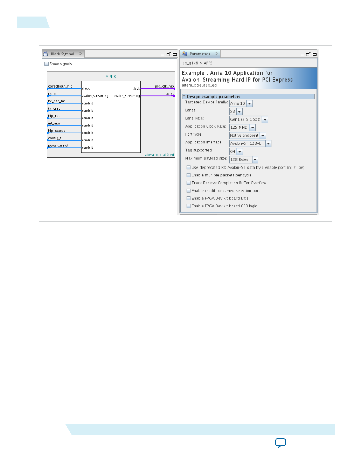
Altera provides example designs to familiarize you with the available functionality. Each design connects
the device under test (DUT) to an application programming platform (APP), labeled APPs in the figure
below. Starting in the Quartus II 14.1 release, if you change these parameters Qsys updates the testbench
Datasheet
to match the parameters you've selected.
Send Feedback
Altera Corporation
Page 17
1-10
Debug Features
Figure 1-4: Example Design Preset Parameters
UG-01145_avst
2015.05.04
You can download the Qsys example designs for the Arria 10 Hard IP for PCI Express from the
<install_dir>/ip/altera/altera_pcie/altera_pcie_a10_ed/example_design/a10 directory.
When you click the Example Design button in the Parameter Editor, you are prompted to specify the
example design location. After example design generation completes, this directory contains one or two
example designs. One is the example design from the <install_dir> that best matches the current parameter
settings. This example design provides a static DUT. The other example design is a customized example
design that matches your parameter settings exactly; starting in the Quartus II software v14.1, this feature
is available for most but not all IP core variations. If this feature is not available for your particular
parameter settings, the Parameter Editor displays a warning.
Debug Features
Debug features allow observation and control of the Hard IP for faster debugging of system-level
problems.
Related Information
Debugging on page 18-1
Altera Corporation
Datasheet
Send Feedback
Page 18

UG-01145_avst
2015.05.04
IP Core Verification
To ensure compliance with the PCI Express specification, Altera performs extensive verification. The
simulation environment uses multiple testbenches that consist of industry-standard bus functional
models (BFMs) driving the PCI Express link interface. Altera performs the following tests in the
simulation environment:
• Directed and pseudorandom stimuli are applied to test the Application Layer interface, Configuration
Space, and all types and sizes of TLPs
• Error injection tests that inject errors in the link, TLPs, and Data Link Layer Packets (DLLPs), and
check for the proper responses
• PCI-SIG® Compliance Checklist tests that specifically test the items in the checklist
• Random tests that test a wide range of traffic patterns
Altera provides example designs that you can leverage to test your PCBs and complete compliance base
board testing (CBB testing) at PCI-SIG, upon request.
Compatibility Testing Environment
Altera has performed significant hardware testing to ensure a reliable solution. In addition, Altera
internally tests every release with motherboards and PCI Express switches from a variety of manufac‐
turers. All PCI-SIG compliance tests are run with each IP core release.
IP Core Verification
1-11
Performance and Resource Utilization
Because the PCIe protocol stack is implemented in hardened logic, it uses no core device resources (no
ALMs and no embedded memory).
Related Information
Fitter Resources Reports
Recommended Speed Grades
Recommended speed grades are pending characterization of production Arria 10 devices.
Related Information
• Area and Timing Optimization
• Altera Software Installation and Licensing Manual
• Setting up and Running Analysis and Synthesis
Steps in Creating a Design for PCI Express
Datasheet
Before you begin
Select the PCIe variant that best meets your design requirements.
Altera Corporation
Send Feedback
Page 19

1-12
Steps in Creating a Design for PCI Express
UG-01145_avst
2015.05.04
• Is your design an Endpoint or Root Port?
• What Generation do you intend to implement?
• What link width do you intend to implement?
• What bandwidth does your application require?
• Does your design require CvP?
1. Select parameters for that variant.
2. Simulate using an Altera-provided example design. All of Altera's static PCI Express example designs
are available under <install_dir>/ip/altera/altera_pcie/. Alternatively, generate an example design that
matches your parameter settings, or create a simulation model and use your own custom or thirdparty BFM. The Qsys Generate menu generates simulation models. Altera supports ModelSim®-Altera
for all IP. The PCIe cores support the Aldec RivieraPro, Cadence NCsim, Mentor Graphics ModelSim,
and Synopsys VCS and VCS-MX simulators.
3. Compile your design using the Quartus II software. If the versions of your design and the Quartus II
software you are running do not match, regenerate your PCIe design.
4. Download your design to an Altera development board or your own PCB. Click on the All Develop‐
ment Kits link below for a list of Altera's development boards.
5. Test the hardware. You can use Altera's SignalTap® II Logic Analyzer or a third-party protocol
analyzer to observe behavior.
6. Substitute your Application Layer logic for the Application Layer logic in Altera's testbench. Then
repeat Steps 3–6. In Altera's testbenches, the PCIe core is typically called the DUT (device under test).
The Application Layer logic is typically called APPS.
Related Information
• Parameter Settings on page 4-1
• Getting Started with the Arria 10 Hard IP for PCI Express on page 2-1
• All Development Kits
Altera Corporation
Datasheet
Send Feedback
Page 20

Getting Started with the Arria 10 Hard IP for PCI
APPS
altpcied_<dev>_hwtcl.v
Hard IP for PCI Express Testbench for Endpoints
Avalon-ST TX
Avalon-ST RX
reset
status
Avalon-ST TX
Avalon-ST RX
reset
status
DUT
<instance_name>_altera_pcie
_a10_hip_<version>
_<generated_string>.v
Root Port Model
altpcie_tbed_<dev>_hwtcl.v
PIPE or
Serial
Interface
Root Port BFM
altpcietb_bfm_rpvar_64b_x8_pipen1b
Root Port Driver and Monitor
altpcietb_bfm_vc_intf
www.altera.com
101 Innovation Drive, San Jose, CA 95134
Express
2015.05.04
UG-01145_avst
Subscribe
This section provides instructions to help you quickly customize, simulate, and compile the Arria 10 Hard
IP for PCI Express IP Core. When you install the Quartus II software you also install the IP Library. This
installation includes design examples for Hard IP for PCI Express under the <install_dir>/ip/altera/altera_
pcie/ directory.
After you install the Quartus II software, you can copy the design examples from the <install_dir>/ip/altera/
altera_pcie/altera_pcie_a10_ed/example_design/a10 directory. This walkthrough uses the Gen1 ×8 Endpoint,
ep_g1x8.qsys. The following figure illustrates the top-level modules of the testbench in which the DUT, a
Gen1 Endpoint, connects to a chaining DMA engine, labeled APPS in the following figure, and a Root
Port model. The simulation can use the parallel PHY Interface for PCI Express (PIPE) or serial interface.
Figure 2-1: Testbench for an Endpoint
Send Feedback
2
Note:
The Quartus II software automatically creates a simulation log file, altpcie_monitor_<dev>_dlhip_tlp_
file_log.log, in your simulation directory. Refer to Understanding Simulation Log File Generation for
details.
Altera provides example designs to help you get started with the Arria 10 Hard IP for PCI Express IP
Core. You can use example designs as a starting point for your own design. The example designs include
scripts to compile and simulate the Arria 10 Hard IP for PCI Express IP Core. This example design
provides a simple method to perform basic testing of the Application Layer logic that interfaces to the
Hard IP for PCI Express.
©
2015 Altera Corporation. All rights reserved. ALTERA, ARRIA, CYCLONE, ENPIRION, MAX, MEGACORE, NIOS, QUARTUS and STRATIX words and logos are
trademarks of Altera Corporation and registered in the U.S. Patent and Trademark Office and in other countries. All other words and logos identified as
trademarks or service marks are the property of their respective holders as described at www.altera.com/common/legal.html. Altera warrants performance
of its semiconductor products to current specifications in accordance with Altera's standard warranty, but reserves the right to make changes to any
products and services at any time without notice. Altera assumes no responsibility or liability arising out of the application or use of any information,
product, or service described herein except as expressly agreed to in writing by Altera. Altera customers are advised to obtain the latest version of device
specifications before relying on any published information and before placing orders for products or services.
ISO
9001:2008
Registered
Page 21
2-2
Qsys Design Flow
For a detailed explanation of this example design, refer to the Testbench and Design Example chapter. If
you choose the parameters specified in this chapter, you can run all of the tests included in Testbench and
Design Example chapter.
For more information about Qsys, refer to System Design with Qsys in the Quartus II Handbook. For more
information about the Qsys GUI, refer to About Qsys in Quartus II Help.
Related Information
• Testbench and Design Example on page 17-1
• Understanding Simulation Log File Generation on page 2-4
• System Design with Qsys
• About Qsys
Qsys Design Flow
Copy the ep_g1x8.qsys design example from the <install_dir>/ip/altera/altera_pcie/altera_pcie/altera_pcie_
a10_ed/example_designs/a10 to your working directory.
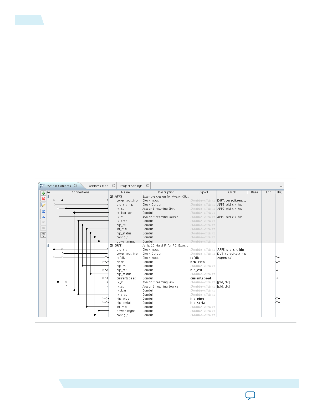
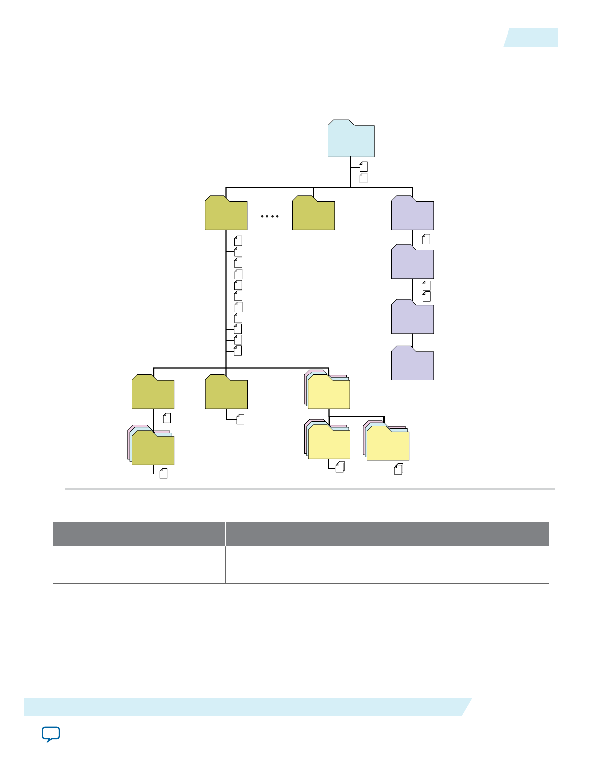
The following figure illustrates this Qsys system.
Figure 2-2: Complete Gen1 ×8 Endpoint (DUT) Connected to Example Design (APPS)
UG-01145_avst
2015.05.04
Altera Corporation
Getting Started with the Arria 10 Hard IP for PCI Express
Send Feedback
Page 22

UG-01145_avst
2015.05.04
The example design includes the following components:
• DUT—This is Gen1 ×8 Endpoint. For your own design, you can select the data rate, number of lanes,
and either Endpoint or Root Port mode.
• APPS—This Root Port BFM configures the DUT and drives read and write TLPs to test DUT
functionality. An Endpoint BFM is available if your PCI Express design implements a Root Port.
Generating the Testbench
1. On the Generate menu, select Generate Testbench System. Specify the parameters listed in the
following table.
Table 2-1: Parameters to Specify on the Generation Tab in Qsys
Parameter Value
Testbench System
Create testbench Qsys system Standard, BFMs for standard Qsys interfaces
Create testbench simulation model Verilog
Generating the Testbench
2-3
Allow mixed-language simulation Turn this option off
Output Directory
Clear output directories for selected generation
Turn this option off
targets
Testbench <working_dir>/ep_g1x8_tb/
2.
Click the Generate button at the bottom of the Generation tab to create the testbench.
Note:
This testbench assumes that you are running the DMA application that the example design
available in the installation directory creates. Otherwise, the testbench tests will probably fail unless
your own testbench has equivalent functionality.
Simulating the Example Design
1. Start your simulation tool. This example uses the ModelSim® software.
2. From the ModelSim transcript window, in the testbench directory, <working_dir>/ep_g1x8_tb/ep_g1x8_
tb/sim/mentor, type the following commands:
a. do msim_setup.tcl
b. ld_debug (This command compiles all design files and elaborates the top-level design without any
optimization.)
c. run -all
Getting Started with the Arria 10 Hard IP for PCI Express
Send Feedback
Altera Corporation
Page 23

2-4
Generating Quartus II Synthesis Files
The simulation includes the following stages:
• Link training
• Configuration
• DMA reads and writes
• Root Port to Endpoint memory reads and writes
Disabling Scrambling to Interpret TLPs at the PIPE Interface
1. Go to <project_directory/ep_g1x8_tb/ep_g1x8_tb/altera_pcie_a10_tbed_140/sim/.
2. Open altpcietb_bfm_top_rp.v.
3. Locate the assignment for test_in[2:1]. Set test_in[2] = 1 and test_in[1] = 0. Changing
test_in[2] = 1 disables data scrambling on the PIPE interface.
4. Save altpcietb_bfm_top_rp.v.
Generating Quartus II Synthesis Files
1. On the Generate menu, select Generate HDL.
2. For Create HDL design files for synthesis, select Verilog.
You can leave the default settings for all other items.
3. Click Generate to generate files for Quartus II synthesis.
4. Click Finish when the generation completes.
UG-01145_avst
2015.05.04
Understanding the Files Generated
Table 2-2: Overview of Qsys Generation Output Files
Directory Description
<testbench_dir>/<variant_name>/synth Includes the top-level HDL file for the Hard IP for
PCI Express.
<testbench_dir>/<variant_name>/sim/<cad_vendor>
Includes the HDL source files and scripts for the
simulation testbench.
For a more detailed listing of the directories and files the Quartus II software generates, refer to Files
Generated for Altera IP Cores in Compiling the Design in the Qsys Design Flow.
Understanding Simulation Log File Generation
Starting with the Quartus II 14.0 software release, simulation automatically creates a log file, altpcie_
monitor_<dev>_dlhip_tlp_file_log.log in your simulation directory.
Table 2-3: Sample Simulation Log File Entries
Time TLP Type Payload
(Bytes)
TLP Header
17989 RX CfgRd0 0004 04000001_0000000F_01080008
17989 RX MRd 0000 00000000_00000000_01080000
Altera Corporation
Getting Started with the Arria 10 Hard IP for PCI Express
Send Feedback
Page 24

UG-01145_avst
2015.05.04
Understanding Physical Placement of the PCIe IP Core
2-5
Time TLP Type Payload
(Bytes)
TLP Header
18021 RX CfgRd0 0004 04000001_0000010F_0108002C
18053 RX CfgRd0 0004 04000001_0000030F_0108003C
18085 RX MRd 0000 00000000_00000000_0108000C
Understanding Physical Placement of the PCIe IP Core
For more information about physical placement of the PCIe blocks, refer to the links below. Contact your
Altera sales representative for detailed information about channel and PLL usage.
Related Information
• Channel Placement and fPLL Usage for the Gen1 and Gen2 Data Rates on page 5-5
• Channel Placement and fPLL and ATX PLL Usage for the Gen3 Data Rate on page 5-7
Adding Virtual Pin Assignment to the Quartus II Settings File (.qsf)
To compile successfully you must add a virtual pin assignment statement for the PIPE interface to
your .qsf file. The PIPE interface is useful for debugging, but is not a top-level interface of the IP core.
1. Browse to the synthesis directory that includes the .qsf for your project, <project_dir>/ep_g1x8/
2. Open ep_g1x8.qsf.
3. Add the following assignment statement:
set_instance_assignment -name VIRTUAL_PIN ON -to hip_pipe_*
4. Save the .qsf file.
Compiling the Design in the Qsys Design Flow
To compile the Qsys design example in the Quartus II software, you must create a Quartus II project and
add your Qsys files to that project.
1. Before compiling, you can optionally turn on two parameters in the testbench. The first parameter
specifies pin assignments that match those for the Altera Development Kit board I/Os. The second
parameter enables the Compliance Base Board (CBB) logic on the development board. In the Gen1 x8
example design, complete the following steps if you want to enable these parameters:
a. Right-click the APPS component and select Edit.
b. Turn on Enable FPGA Dev kit board I/Os.
c. Turn on Enable FPGA Dev kit board CBB logic.
d. Click Finish.
e. On the Generate menu, select Generate Testbench System and then click Generate.
f. On the Generate menu, select Generate HDL and then click Generate. (You can use the same
parameters that are specified in Generating the Testbench earlier in this chapter).
2. In the Quartus II software, click the New Project Wizard icon.
3. Click Next in the New Project Wizard: Introduction (The introduction does not appear if you
previously turned it off.)
4. On the Directory, Name, Top-Level Entity page, enter the following information:
Getting Started with the Arria 10 Hard IP for PCI Express
Send Feedback
Altera Corporation
Page 25

2-6
Compiling the Design in the Qsys Design Flow
a. The working directory shown is correct. You do not have to change it.
b. For the project name, click the browse button browse to the synthesis directory that includes your
Qsys project, <working_dir>/ep_g1x8/synth and click Choose. If the top-level design entity and Qsys
system names are identical, the Quartus II software treats the Qsys system as the top-level design
entity.
c. For What is the name of this project, select your variant name ep_g1x8. Then click Open. If the
top-level design entity and Qsys system names are identical, the Quartus II software treats the Qsys
system as the top-level design entity.
d. For Project Type select Empty project.
5. Click Next to display the Add Files page.
6. Complete the following steps to add the Quartus II IP File ( .qip )to the project:
a. Click the browse button. The Select File dialog box appears.
b. Browse up one level to <working_dir>/ep_g1x8/ button.
c. In the Files of type list, select IP Variation Files (*.qip *.sip).
d. Click ep_g1x8.qip and then click Open.
e. On the Add Files page, click Add.
7. Click Next to display the Device page.
8. On the Family & Device Settings page, choose the following target device family and options:
UG-01145_avst
2015.05.04
a. In the Family list, select Arria 10 (GX/SX/GT).
b. In the Devices list, select Arria 10 All.
c. In the Devices list, select All.
d. In the Available devices list, select the appropriate device. For Arria 10 ES2 development kits, select
10AX115S1F45I3SGE2.
9. Click Next to close this page and display the EDA Tool Settings page.
10.From the Simulation list, select ModelSim®. From the Format list, select the HDL language you
intend to use for simulation.
11.Click Next to display the Summary page.
12.Check the Summary page to ensure that you have entered all the information correctly.
13.Click Finish to create the Quartus II project.
14.Before compiling, you must assign I/O standards to the pins of the device. Refer to Making Pin
Assignments to Assign I/O Standard to Serial Data Pins for instructions.
15.You must connect the pin_perst reset signal to the correcsponding nPERST pin of the device. Refer to
the definition of pin_perst in the Reset, Status, and Link Training Signals section for more informa‐
tion.
16.Next, set the value of the test_in bus to a value that is compatible for hardware testing. In Qsys design
example provided, test_in is a top-level port.
a. Comment out the test_in port in the top-level Verilog generated file.
b. Add the following declaration, wire[31:0] test_in, to the same top-level Verilog file.
c. Assign hip_ctrl_test_in = 32'hA8.
d. Connect test_in to hip_ctrl_test_in.
17.To compile your design using the Quartus II software, on the Processing menu, click Start Compila‐
Altera Corporation
Refer to the definition of test_in in the Test Signals section for more information about the bits of the
test_in bus.
tion. The Quartus II software then performs all the steps necessary to compile your design.
Getting Started with the Arria 10 Hard IP for PCI Express
Send Feedback
Page 26
<your_testbench>_tb.csv
<your_testbench>_tb.spd
<your_ip>.cmp - VHDL component declaration file
<your_ip>.ppf - XML I/O pin information file
<your_ip>.qip - Lists IP synthesis files
<your_ip>.sip - Contains assingments for IP simulation files
<your_ip>.v or .vhd
Top-level IP synthesis file
<your_ip>.v or .vhd
Top-level simulation file
<simulator_setup_scripts>
<your_ip>.qsys - System or IP integration file
<your_ip>_bb.v - Verilog HDL black box EDA synthesis file
<your_ip>_inst.v or .vhd - Sample instantiation template
<your_ip>_generation.rpt - IP generation report
<your_ip>.debuginfo - Contains post-generation information
<your_ip>.html - Connection and memory map data
<your_ip>.bsf - Block symbol schematic
<your_ip>.spd - Combines simulation scripts for multiple cores
<your_ip>_tb.qsys
Testbench system file
<your_ip>.sopcinfo - Software tool-chain integration file
<project directory>
<EDA tool setup
scripts>
<your_ip>
IP variation files
<testbench>_tb
testbench system
sim
Simulation files
synth
IP synthesis files
sim
simulation files
<EDA tool name>
Simulator scripts
<testbench>_tb
<ip subcores> n
Subcore libraries
sim
Subcore
Simulation files
synth
Subcore
synthesis files
<HDL files>
<HDL files>
<your_ip> n
IP variation files
testbench files
UG-01145_avst
2015.05.04
Files Generated for Altera IP Cores
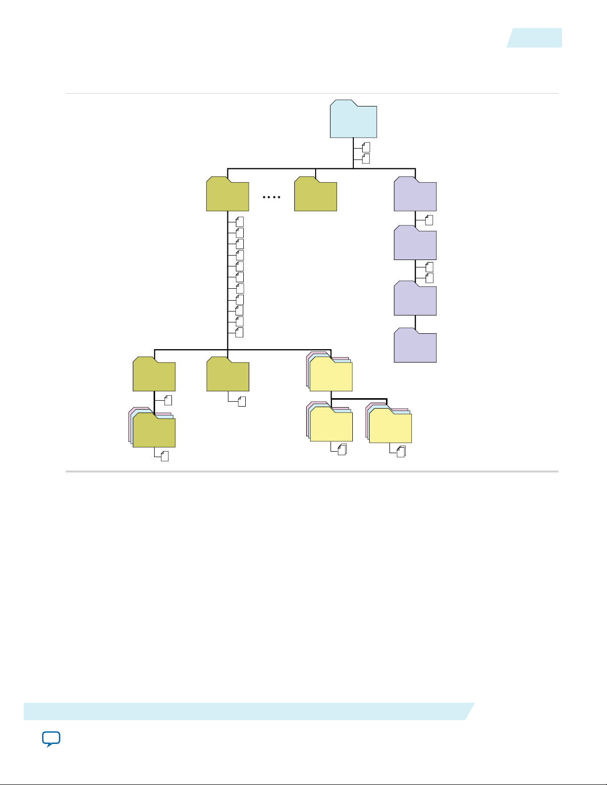
Figure 2-3: IP Core Generated Files
Modifying the Example Design
2-7
Related Information
• Making Pin Assignments to Assign I/O Standard to Serial Data Pins on page 14-1
• Test Signals on page 6-62
• Reset, Status, and Link Training Signals on page 6-31
• Generating the Testbench on page 2-3
• Simulating the Example Design on page 3-5
• Simulating the Example Design on page 3-5
Modifying the Example Design
Getting Started with the Arria 10 Hard IP for PCI Express
Send Feedback
To use this example design as the basis of your own design, replace the Chaining DMA Example shown in
the following figure with your own Application Layer design. Then modify the Root Port BFM driver to
generate the transactions needed to test your Application Layer.
Altera Corporation
Page 27
Hard IP for PCI Express
Altera FPGA
PCB
Root
Port
BFM
perstn (npor)
Reset
APPS DUT
Chaining DMA
(User Application)
Transaction Layer
Data Link Layer
PHY MAC Layer
PHY IP Core for PCI Express
2-8
Using the IP Catalog To Generate Your Arria 10 Hard IP for PCI Express as a Separate Component
Figure 2-4: Testbench for PCI Express
UG-01145_avst
2015.05.04
Using the IP Catalog To Generate Your Arria 10 Hard IP for PCI Express as a Separate
Component
Altera Corporation
You can also instantiate the Arria 10 Hard IP for PCI Express IP Core as a separate component for
integration into your project.
You can use the Quartus II IP Catalog and IP Parameter Editor to select, customize, and generate files
representing your custom IP variation. The IP Catalog (Tools > IP Catalog) automatically displays IP
cores available for your target device. Double-click any IP core name to launch the parameter editor and
generate files representing your IP variation.
For more information about the customizing and generating IP Cores refer to Specifying IP Core
Parameters and Options in Introduction to Altera IP Cores. For more information about upgrading older
IP cores to the current release, refer to Upgrading Outdated IP Cores in Introduction to Altera IP Cores.
Related Information
• Qsys Design Flow on page 2-2
• Introduction to Altera IP Cores
• Managing Quartus II Projects
Getting Started with the Arria 10 Hard IP for PCI Express
Send Feedback
Page 28
<your_testbench>_tb.csv
<your_testbench>_tb.spd
<your_ip>.cmp - VHDL component declaration file
<your_ip>.ppf - XML I/O pin information file
<your_ip>.qip - Lists IP synthesis files
<your_ip>.sip - Contains assingments for IP simulation files
<your_ip>.v or .vhd
Top-level IP synthesis file
<your_ip>.v or .vhd
Top-level simulation file
<simulator_setup_scripts>
<your_ip>.qsys - System or IP integration file
<your_ip>_bb.v - Verilog HDL black box EDA synthesis file
<your_ip>_inst.v or .vhd - Sample instantiation template
<your_ip>_generation.rpt - IP generation report
<your_ip>.debuginfo - Contains post-generation information
<your_ip>.html - Connection and memory map data
<your_ip>.bsf - Block symbol schematic
<your_ip>.spd - Combines simulation scripts for multiple cores
<your_ip>_tb.qsys
Testbench system file
<your_ip>.sopcinfo - Software tool-chain integration file
<project directory>
<EDA tool setup
scripts>
<your_ip>
IP variation files
<testbench>_tb
testbench system
sim
Simulation files
synth
IP synthesis files
sim
simulation files
<EDA tool name>
Simulator scripts
<testbench>_tb
<ip subcores> n
Subcore libraries
sim
Subcore
Simulation files
synth
Subcore
synthesis files
<HDL files>
<HDL files>
<your_ip> n
IP variation files
testbench files
UG-01145_avst
2015.05.04
Files Generated for Altera IP Cores
The Quartus II software generates the following IP core output file structure:
Figure 2-5: IP Core Generated Files
Files Generated for Altera IP Cores
2-9
Table 2-4: IP Core Generated Files
File Name Description
<my_ip>.qsys
Getting Started with the Arria 10 Hard IP for PCI Express
Send Feedback
The Qsys system or top-level IP variation file. <my_ip> is the name
that you give your IP variation.
Altera Corporation
Page 29

2-10
Files Generated for Altera IP Cores
File Name Description
<system>.sopcinfo Describes the connections and IP component parameterizations in
your Qsys system. You can parse its contents to get requirements
when you develop software drivers for IP components.
Downstream tools such as the Nios II tool chain use this file.
The .sopcinfo file and the system.h file generated for the Nios II tool
chain include address map information for each slave relative to each
master that accesses the slave. Different masters may have a different
address map to access a particular slave component.
<my_ip>.cmp The VHDL Component Declaration (.cmp) file is a text file that
contains local generic and port definitions that you can use in VHDL
design files.
UG-01145_avst
2015.05.04
<my_ip>.html
A report that contains connection information, a memory map
showing the address of each slave with respect to each master to
which it is connected, and parameter assignments.
<my_ip>_generation.rpt IP or Qsys generation log file. A summary of the messages during IP
generation.
<my_ip>.debuginfo Contains post-generation information. Used to pass System Console
and Bus Analyzer Toolkit information about the Qsys interconnect.
The Bus Analysis Toolkit uses this file to identify debug components
in the Qsys interconnect.
<my_ip>.qip
Contains all the required information about the IP component to
integrate and compile the IP component in the Quartus II software.
<my_ip>.csv Contains information about the upgrade status of the IP component.
<my_ip>.bsf A Block Symbol File (.bsf) representation of the IP variation for use
in Quartus II Block Diagram Files (.bdf).
<my_ip>.spd
Required input file for ip-make-simscript to generate simulation
scripts for supported simulators. The .spd file contains a list of files
generated for simulation, along with information about memories
that you can initialize.
<my_ip>.ppf The Pin Planner File (.ppf) stores the port and node assignments for
<my_ip>_bb.v You can use the Verilog black-box (_bb.v) file as an empty module
<my_ip>.sip Contains information required for NativeLink simulation of IP
<my_ip>_inst.v or _inst.vhd HDL example instantiation template. You can copy and paste the
Altera Corporation
IP components created for use with the Pin Planner.
declaration for use as a black box.
components. You must add the .sip file to your Quartus project.
contents of this file into your HDL file to instantiate the IP variation.
Getting Started with the Arria 10 Hard IP for PCI Express
Send Feedback
Page 30

UG-01145_avst
2015.05.04
<my_ip>.regmap If the IP contains register information, the .regmap file generates.
Files Generated for Altera IP Cores
File Name Description
The .regmap file describes the register map information of master
and slave interfaces. This file complements the .sopcinfo file by
providing more detailed register information about the system. This
enables register display views and user customizable statistics in
System Console.
2-11
<my_ip>.svd
<my_ip>.v
or
<my_ip>.vhd
mentor/
aldec/
/synopsys/vcs
/synopsys/vcsmx
Allows HPS System Debug tools to view the register maps of
peripherals connected to HPS within a Qsys system.
During synthesis, the .svd files for slave interfaces visible to System
Console masters are stored in the .sof file in the debug section.
System Console reads this section, which Qsys can query for register
map information. For system slaves, Qsys can access the registers by
name.
HDL files that instantiate each submodule or child IP core for
synthesis or simulation.
Contains a ModelSim® script msim_setup.tcl to set up and run a
simulation.
Contains a Riviera-PRO script rivierapro_setup.tcl to setup and run a
simulation.
Contains a shell script vcs_setup.sh to set up and run a VCS
®
simulation.
Contains a shell script vcsmx_setup.sh and synopsys_ sim.setup file to
set up and run a VCS MX® simulation.
/cadence
Contains a shell script ncsim_setup.sh and other setup files to set up
and run an NCSIM simulation.
/submodules Contains HDL files for the IP core submodule.
<child IP cores>/ For each generated child IP core directory, Qsys generates /synth and /
sim sub-directories.
Getting Started with the Arria 10 Hard IP for PCI Express
Send Feedback
Altera Corporation
Page 31

Getting Started with the Configuration Space
www.altera.com
101 Innovation Drive, San Jose, CA 95134
Bypass Mode Qsys Example Design
2014.08.18
UG-01145_avst
Subscribe
This Qsys design example demonstrates Configuration Space Bypass mode for the Arria 10 Hard IP for
PCI Express IP Core. A Root Port BFM provides stimulus to the Endpoint design. The Endpoint bypasses
the standard Configuration Space to access the custom Configuration Space and memory of two
functions. The Configuration Space Bypass Example Design performs the following functions:
• Accepts Configuration, Memory, and Message TLPs on the Arria 10 Hard IP for PCI Express RX
Avalon-ST interface
• Translates Type 0 Configuration Read and Configuration Write Requests to Avalon-MM read and
write requests that target the Configuration Space of either Function 0 or Function 1.
• Responds to invalid Type 0 Configuration Requests with an Unsupported Request (UR) status in a
Completion Message.
• Converts single dword Memory Read and Memory Write Requests to access 32-bit registers of the
target function using the Avalon-MM interface.
• Maps two contiguous MBytes of memory for the two functions with the first MByte for Function 0 and
the second MByte for Function 1.
• Sets up two registers for each function.
• Drops the following invalid Write Requests:
Send Feedback
3
• Memory Write Requests with a payload of more than one dword
• Messages with data
• Returns Completer Abort (CA) status in Completion message for invalid Memory Read Requests such
as Memory Read Requests with a payload greater than one dword.
• Returns a Completion Status of Successful Completion for valid Configuration Requests to Function 0
and Function 1.
The following figure illustrates, the components of the Configuration Space Bypass Mode Qsys Example
Design. The example design includes the following components:
• DUT: The Arria 10 Hard IP for PCI Express. The example turns on the Enable Configuration Space
Bypass parameter.
• APPS: The Configuration Space Bypass application demonstrates Configuration Space Bypass mode.
• pcie_reconfig_driver_0: The PCIe Reconfig Driver drives the Transceiver Reconfiguration Controller.
This driver is a plain text Verilog HDL file that you can modify if necessary to meet your system
requirements.
©
2015 Altera Corporation. All rights reserved. ALTERA, ARRIA, CYCLONE, ENPIRION, MAX, MEGACORE, NIOS, QUARTUS and STRATIX words and logos are
trademarks of Altera Corporation and registered in the U.S. Patent and Trademark Office and in other countries. All other words and logos identified as
trademarks or service marks are the property of their respective holders as described at www.altera.com/common/legal.html. Altera warrants performance
of its semiconductor products to current specifications in accordance with Altera's standard warranty, but reserves the right to make changes to any
products and services at any time without notice. Altera assumes no responsibility or liability arising out of the application or use of any information,
product, or service described herein except as expressly agreed to in writing by Altera. Altera customers are advised to obtain the latest version of device
specifications before relying on any published information and before placing orders for products or services.
ISO
9001:2008
Registered
Page 32

to PCIe Root Port
and Host System
Configuration
Bypass Top
(cfbp_top)
APPS: Config Bypass Example
Root Port
(cfbp_app_example)
DUT: Hard IP for PCIe
Using Configuration Bypass
Mode Endpoint
Function 0
Function 1
2 MByte Memory
Reset
(rs_hip)
Configuration Space
Configuration Space
Local Management
Interface (LMI)
Function 0 Registers
Function 1 Registers
pcie_reconfig_driver_0
3-2
Copying the Configuration Space Bypass Mode Example Design
Figure 3-1: Configuration Bypass Mode Qsys Example Design
UG-01145_avst
2014.08.18
Copying the Configuration Space Bypass Mode Example Design
Follow these steps to copy the Configuration Space Bypass Mode Qsys Example Design to your working
directory:
1. Copy the example design, pcie_cfbp_g2x8_ast256.qsys, from the installation directory <install_dir>/ip/
altera/altera_pcie/altera_pcie_a10_ed/example_design/a10 to your working directory.
2. Copy the Qsys wrapper file for the Configuration Space Bypass application logic, altera_pcie_cfgbp_ed_
hw.tcl, from the installation directory <install_dir>/ip/altera/altera_pcie/altera_pcie_a10_ed/example_design/
a10 to your working directory.
3. Rename the pcie_cfbp_g2x8_ast256.qsys top.qys. Renaming is necessary because the testbench defines
4. Start Qsys by typing qsys-edit and open top.qsys when prompted by Qsys.
The following figure shows the complete system.
top.v as the top-level wrapper. Qsys creates top.v from top.qsys when you generate the system.
Altera Corporation
Getting Started with the Configuration Space Bypass Mode Qsys Example Design
Send Feedback
Page 33

UG-01145_avst
2014.08.18
Figure 3-2: Configuration Bypass Qsys System
Generating the Qsys System
3-3
1. Note the following parameter settings for the Configuration Space Bypass Example Design:
• For the DUT, the Enable Configuration Bypass parameter is turned on under the System Settings
banner.
• The Base Address Registers specify BAR0 as 1 MByte - 20 bits of 64-bit prefetchable memory for
each function. In Configuration Space Bypass Mode, the BAR registers inside the Hard IP for PCI
Express are not used. The Application Layer implements the Configuration Space for each function.
• For testbench compatibility, the Config-Bypass App Example, labeled APPs, must retain a Device ID
of 0xE001 (5734510) and a Vendor ID of 0x1172 (446610).
Generating the Qsys System
On the Qsys Generate menu, select Generate Testbench System. Specify the parameters listed in the
following table.
Getting Started with the Configuration Space Bypass Mode Qsys Example Design
Send Feedback
Altera Corporation
Page 34

3-4
Generating Quartus II Synthesis Files
Table 3-1: Parameters to Specify on the Generation Tab in Qsys
Parameter Value
Create testbench Qsys system Standard, BFMs for standard Avalon interfaces
Create simulation model Verilog
Allow mixed-language simulation Turn this option off
Output Directory
Path <working_dir>/top
Testbench <working_dir>/top/testbench
1. Click Generate to generate the simulation and testbench files.
2. On the File menu, click Save.
UG-01145_avst
2014.08.18
Generating Quartus II Synthesis Files
1. On the Generate menu, select Generate HDL.
2. For Create HDL design files for synthesis, select Verilog.
You can leave the default settings for all other items.
3. Click Generate to generate files for Quartus II synthesis.
4. Click Finish when the generation completes.
Understanding the Generated Files
Table 3-2: Qsys Generation Output Files
Directory Description
<testbench_dir>/<variant_name>/synthesis Includes the top-level HDL file for the Hard IP for
PCI Express and the .qip file that lists all of the
necessary assignments and information required to
process the IP core in the Quartus II compiler.
Generally, a single .qip file is generated for each IP
core. These files are used for Quartus II synthesis.
<testbench_dir>/<variant_name>/synthesis/submodules
Includes the HDL files necessary for Quartus II
synthesis.
<testbench_dir>/<variant_name>/testbench/<cad_
vendor>
Altera Corporation
Includes the HDL source files and scripts for the
simulation testbench.
Getting Started with the Configuration Space Bypass Mode Qsys Example Design
Send Feedback
Page 35

UG-01145_avst
2014.08.18
Understanding Simulation Log File Generation
Starting with the Quartus II 14.0 software release, simulation automatically creates a log file, altpcie_
monitor_<dev>_dlhip_tlp_file_log.log in your simulation directory.
Table 3-3: Sample Simulation Log File Entries
Understanding Simulation Log File Generation
3-5
Time TLP Type Payload
(Bytes)
17989 RX CfgRd0 0004 04000001_0000000F_01080008
17989 RX MRd 0000 00000000_00000000_01080000
18021 RX CfgRd0 0004 04000001_0000010F_0108002C
18053 RX CfgRd0 0004 04000001_0000030F_0108003C
18085 RX MRd 0000 00000000_00000000_0108000C
Simulating the Example Design
Follow these steps to simulate the Qsys system using ModelSim:
1. In a terminal window, change to the <working_dir>/top/testbench/mentor directory.
2. Start the ModelSim simulator by typing vsim.
3. To compile the simulation, type the following commands in the terminal window:
• source msim_setup.tcl (The msim_setup.tcl file defines aliases.
• ld_debug (The ld_debug command argument stops optimizations, improving visibility in the
ModelSim waveforms. )
The following figure shows the design hierarchy for the Configuration Space Bypass Example Design after
compilation.
TLP Header
Figure 3-3: Design Hierarchy for the Configuration Space Bypass Example Design for 256-Bit Avalon-ST
Interface
Getting Started with the Configuration Space Bypass Mode Qsys Example Design
Send Feedback
Altera Corporation
Page 36

3-6
Timing for Configuration Read to Function 0 for the 256-Bit Avalon-ST Interface
UG-01145_avst
1. To observe the simulation, on the ModelSim View menu, select wave. Then add some key interfaces to
the wave window. The following four interfaces under the /top_tb/top_inst/apps/altpcierd_cfbp_top/
cfgbp_app_ctrl/genblk1 illustrate the TX and RX interfaces, the current state, and configuration.
• *RxSt*
• *TxSt*
• *Rxm*
• *_state*
• cfg_*
2. To run the simulation, type the following command: run -all
Note: By default, the simulation is serial, to simulate using the parallel PIPE interface, you can change the
default value of the serial_sim_hwtcl parameter from 1 to 0 in altera_pcie_cfgbp_ed/top/testbench/
top_tb/simulation/top_tb.v. After changing that value, you must recompile the simulation to pick up
the new value of the serial_sim_hwtcl parameter before running the simulation.
Timing for Configuration Read to Function 0 for the 256-Bit Avalon-ST Interface
The following timing diagram illustrates a Configuration Read to Function 0 starting at time 60568 ns in
the simulation.
2014.08.18
Altera Corporation
Getting Started with the Configuration Space Bypass Mode Qsys Example Design
Send Feedback
Page 37

RxStMask_o
RxStSop_i
RxStEop_i
RxStValid_i
RxStReady_o
RxStData_i[255:0]
cfg_addr_o[31:0]
cfg_rden_o
cfg_wren_o
cfg_be_o[3:0
cfg_rddatavalid _
cfg_rddata_i[31:0]
cfg_readresponse_i[2:0]
TxStReady_i
TxStSop_o
TxStEop_o
TxStValid_o
TxStEmpty_o[1:0]
TxStData_o[255:0]
rx_state[10:0]
rxcfg_state[4:0]
tx_state[1:0]
1
’b0000000000000000000 .
000 003 005 021 009 000
E0011172
...E00111720000000000000044A000001
0108000001120004
05
3
1
2
3
4
UG-01145_avst
2014.08.18
Figure 3-4: Configuration Read to Function 0
Timing for Configuration Read to Function 0 for the 256-Bit Avalon-ST Interface
3-7
Getting Started with the Configuration Space Bypass Mode Qsys Example Design
Altera Corporation
Send Feedback
Page 38

3-8
Timing for Configuration Write to Function 0 for the 256-Bit Avalon-ST Interface
UG-01145_avst
The preceding timing diagram illustrates the following sequence of events:
1. The Application Layer indicates it is ready to receive requests by asserting RxSTReady_o. The RX
Avalon-ST interface initiates a Configuration Read, asserting its RxStSop_i and RxStValid_i signals.
2. At the falling edge of RxStSop_i, the Avalon-MM master interface asserts cfg_rden_o and specifies
the address on cfg_addr_o[31:0].
3. The Function 0 Avalon-MM slave interface asserts cfg_rddavalid_i and drives the data on
cfg_rddata_i[31:0].
4. On the falling edge of cfg_rddavalid_i, the TX interface asserts TxStSop_o and TxStValid_o and
drives the data of TxStData_o[255:0]. This is the Completion Request to the host corresponding to
its Configuration Read Request.
Timing for Configuration Write to Function 0 for the 256-Bit Avalon-ST Interface
The following timing diagram illustrates a configuration write to Function 0 starting at time 61859 ns in
the simulation.
The timing diagram illustrates the following sequence of events:
1. The Application Layer indicates it is ready to receive requests by asserting RxSTReady_o. The RX
Avalon-ST interface initiates a Configuration Write, asserting its RxStSop_i and RxStValid_i
signals.
2. At the falling edge of RxStSop_i, the Avalon-MM master interface asserts cfg_wren_o and specifies
the data on cfg_wrdata_o[31:0]. The Master interface also assert cfg_writeresponserequest_o, to
request completion status from Function 0.
3. On the falling edge of cfg_writeresponserequest_o, Function 0 asserts cfg_writeresponse-
valid_i.
4. On the falling edge of cfg_writeresponsevalid_i, the TX interface asserts TxStSop_o and
TxStValid_o and drives the completion data on TxStData_o[255:0].
2014.08.18
Altera Corporation
Getting Started with the Configuration Space Bypass Mode Qsys Example Design
Send Feedback
Page 39

RxStMask_o
RxStSop_i
RxStEop_i
RxStValid_i
RxStReady_o
RxStData_i[255:0
cfg_addr_o[31:0]
cfg_rden_o
cfg_wren_
cfg_writeresponserequest _
cfg_wrdata_o[31:0]
cfg_writeresponsevalid
cfg_writeresponse_i[2:0]
cfg_waitrequest _
cfg_be_o[3:0]
TxStReady_i
TxStSop_o
TxStEop_o
TxStValid_o
TxStData_o[255:0]
rx_state[10:0]
rxavl_state[3:0]
rxcfg_state[4:0]
tx_state[1:0]
000000000000.0000000
00000060
01000004
.
0000000 ..800040A000001
00000000000000000000000601000004000000F440800100000F4408001
.
000 003 005 021 009 081 000 003
03 09 11
3
0
1
2
3
UG-01145_avst
2014.08.18
Figure 3-5: Configuration Write to Function 0
Timing for Memory Write and Read of Function 1 256-Bit Avalon-ST Interface
3-9
Timing for Memory Write and Read of Function 1 256-Bit Avalon-ST Interface
The following timing diagram illustrates memory to Function 1 which occurs in the simulation starting at
time 99102 ns.
Getting Started with the Configuration Space Bypass Mode Qsys Example Design
Altera Corporation
Send Feedback
Page 40

RxStMask_o
RxStSop_i
RxStEop_i
RxStValid_i
RxStReady_o
TxStReady_i
TxStSop_o
TxStEop_o
TxStValid_ o
rx_state[10:0]
rxavl_state[3:0]
rxcfg_state[4:0]
tx_state[1:0]
RxmAddress_0_o[19:0]
RxmFunc1Sel _o
RxmWrite_0_o
RxmWriteData_0_o[31:0]
RxmWaitRequest_0
RxmRead_0_ o
RxmReadDataValid_0 _
RxmReadData_0_i[31:0]
000 003
90030 00000
005 021 041 000 003 005 021 041 00
3 9 0 5
3
BABEFACE
BABEFACE
1 3
4
5 6
2
3-10
Timing for Memory Write and Read of Function 1 256-Bit Avalon-ST Interface
Figure 3-6: Timing for Memory Write and Read of Function 1
UG-01145_avst
2014.08.18
Altera Corporation
Getting Started with the Configuration Space Bypass Mode Qsys Example Design
Send Feedback
Page 41

UG-01145_avst
2014.08.18
Partial Transcript for Configuration Space Bypass Simulation
The timing diagram illustrates the following sequence of events:
1. The Application Layer indicates it is ready to receive requests by asserting RxSTReady_o. The RX
Avalon-ST interface initiates a Memory Write to Function 1, asserting its RxStSop_i and
RxStValid_i signals.
2. At the falling edge of RxStSop_i, RxmFunc1Sel_o is asserted and the write data is driven on RxmWrite-
Data_0_o[31:0]. The Memory Write to Function 1 completes when the data is written.
3. The Application Layer indicates it is ready to receive requests by asserting RxSTReady_o. The RX
Avalon-ST interface initiates a Memory Read to Function 1, asserting its RxStSop_i and RxStValid_i
signals.
4. After the falling edge of RxStSop_i, the RX Avalon-MM master interface asserts RxmRead_0_o to
Function 1.
5. At the falling edge of RxmRead_0_o, Function 1 asserts RxmReadDataValid_0 and drives the data on
RxmReadData_0_i[ 31:0].
6. The host receives the completion data when TxStValid_o, TxStSop_o, and TxStEop_o are asserted.
Partial Transcript for Configuration Space Bypass Simulation
The driver performs the following transactions with status of the transactions displayed in the ModelSim
simulation message window:
3-11
• Various configuration reads and writes to the Avalon-MM Arria 10 Hard IP for PCI Express in your
system after the link is initialized
• Register writes, reads and compares to both functions
• Burst memory writes, reads, and compares to both functions
The following example shows the transcript from a successful simulation run.
Example 3-1: Transcript from ModelSim Simulation of Gen1 x4 Endpoint
# INFO: 464 ns Completed initial configuration of Root Port.
# 495000: INFO: top_tb.top_inst_reset_bfm.reset_deassert: Reset deasserted
# INFO: 3657 ns RP LTSSM State: DETECT.ACTIVE
# INFO: 4425 ns RP LTSSM State: POLLING.ACTIVE
# INFO: 17257 ns RP LTSSM State: DETECT.QUIET
# INFO: 20473 ns RP LTSSM State: DETECT.ACTIVE
# INFO: 21193 ns RP LTSSM State: POLLING.ACTIVE
# INFO: 29909 ns EP LTSSM State: DETECT.ACTIVE
# INFO: 30949 ns EP LTSSM State: POLLING.ACTIVE
# INFO: 33957 ns EP LTSSM State: POLLING.CONFIG
# INFO: 34025 ns RP LTSSM State: DETECT.QUIET
# INFO: 37241 ns RP LTSSM State: DETECT.ACTIVE
# INFO: 37961 ns RP LTSSM State: POLLING.ACTIVE
# INFO: 39945 ns RP LTSSM State: POLLING.CONFIG
# INFO: 41033 ns RP LTSSM State: CONFIG.LINKWIDTH.START
# INFO: 41445 ns EP LTSSM State: CONFIG.LINKWIDTH.START
# INFO: 41765 ns EP LTSSM State: CONFIG.LINKWIDTH.ACCEPT
# INFO: 42057 ns RP LTSSM State: CONFIG.LINKWIDTH.ACCEPT
# INFO: 42249 ns RP LTSSM State: CONFIG.LANENUM.WAIT
# INFO: 42789 ns EP LTSSM State: CONFIG.LANENUM.WAIT
# INFO: 43033 ns RP LTSSM State: CONFIG.LANENUM.ACCEPT
# INFO: 43109 ns EP LTSSM State: CONFIG.LANENUM.ACCEPT
# INFO: 43225 ns RP LTSSM State: CONFIG.COMPLETE
# INFO: 43685 ns EP LTSSM State: CONFIG.COMPLETE
# INFO: 44953 ns RP LTSSM State:CONFIG.IDLE
# INFO: 47941 ns EP LTSSM State: CONFIG.IDLE
Getting Started with the Configuration Space Bypass Mode Qsys Example Design
Send Feedback
Altera Corporation
Page 42

3-12
Partial Transcript for Configuration Space Bypass Simulation
# INFO: 48089 ns RP LTSSM State: L0
# INFO: 48133 ns EP LTSSM State: L0
# INFO: 48226 ns Configuring Bus 000, Device 000, Function 00
# INFO: 48226 ns RP Read Only Configuration Registers:
# INFO: 48226 ns Vendor ID: 1556
# INFO: 48226 ns Device ID: 5555
# INFO: 48226 ns Revision ID: 00
# INFO: 48226 ns Class Code: 040000
# INFO: 48706 ns ECRC Check Capable: Supported
# INFO: 48706 ns ECRC Generation Capable: Supported
# INFO: 48738 ns RP PCI Express Slot Capability
# INFO: 48738 ns Power Controller: Not Present
# INFO: 48738 ns MRL Sensor: Not Present
# INFO: 48738 ns Attention Indicator: Not Present
# INFO: 48738 ns Power Indicator: Not Present
# INFO: 48738 ns Hot-Plug Surprise: Not Supported
# INFO: 48738 ns Hot-Plug Capable: Not Supported
# INFO: 48738 ns Slot Power Limit Value: 0
# INFO: 48738 ns Slot Power Limit Scale: 0
# INFO: 48738 ns Physical Slot Number: 0
# INFO: 48738 ns Activity_toggle flag is set
# INFO: 48802 ns RP PCI Express Link Status Register (0081):
# INFO: 48802 ns RP PCI Express Max Link Speed (0002):
# INFO: 48802 ns RP PCI Express Current Link Speed (0001):
# INFO: 48802 ns Negotiated Link Width: x8
# INFO: 48802 ns Slot Clock Config: Local Clock Used
# INFO: 48834 ns Current Link Speed: 2.5GT/s
# INFO: 48889 ns RP LTSSM State: RECOVERY.RCVRLOCK
# INFO: 49669 ns EP LTSSM State: RECOVERY.RCVRLOCK
# INFO: 50501 ns EP LTSSM State: RECOVERY.RCVRCFG
# INFO: 51209 ns RP LTSSM State: RECOVERY.RCVRCFG
# INFO: 48889 ns RP LTSSM State: RECOVERY.RCVRLOCK
# INFO: 53669 ns EP LTSSM State: RECOVERY.SPEED
# INFO: 54721 ns RP LTSSM State: RECOVERY.RCVRLOCK
# INFO: 54746 ns Wait for Link to enter L0 after negotiated to
# the expected speed of EP Target Link Speed 0002):
# INFO: 53337 ns RP LTSSM State: RECOVERY.SPEED
# INFO: 55235 ns EP LTSSM State: RECOVERY.RCVRLOCK
# INFO: 56299 ns EP LTSSM State: RECOVERY.RCVRCFG
# INFO: 57163 ns RP LTSSM State: RECOVERY.RCVRCFG
# INFO: 57707 ns RP LTSSM State: RECOVERY.IDLE
# INFO: 57979 ns EP LTSSM State: RECOVERY.IDLE
# INFO: 58035 ns RP LTSSM State: L0
# INFO: 58075 ns EP LTSSM State: L0
# INFO: 58090 ns New Link Speed: 5.0GT/s
# INFO: 58106 ns RP PCI Express Link Control Register (0000):
# INFO: 58106 ns Common Clock Config: Local Clock
# INFO: 70602 ns Completed configuration of Endpoint BARs.
# INFO: 70602 ns TASK:my_test Setup
# INFO: 70602 ns TASK:my_test Write to 32bit register at
# addr = 0x0 with wdata=0xBABEFACE
# INFO: 70610 ns TASK:my_test Read from 32bit register at
# addr 0x00000000
# INFO: 71298 ns TASK:my_test Register compare matches!
# INFO: 71298 ns TASK:my_test Write to 32bit register at
# 0x00000004 Actual 0x12345678
# INFO: 71306 ns TASK:my_test => 1.22 Read from 32bit register
# at addr = 0x00000004
# INFO: 71994 ns TASK:my_test => 1.23 Register compare matches!
# INFO 71994 ns TASK:my_test => 2.11 Fill write memory with
# QWORD_INC pattern
# INFO: 71994 ns TASK:my_test Memory write burst at addr=0x00
# with wdata=0x10203040
# INFO: 72002 ns TASK:my_test => 2.21 Memory Read burst
# INFO: 72690 ns TASK:my_test Memory write burst at addr=0x04
# with wdata=0x10203040
# INFO: 72698 ns TASK:my_test Memory Read burst
UG-01145_avst
2014.08.18
Altera Corporation
Getting Started with the Configuration Space Bypass Mode Qsys Example Design
Send Feedback
Page 43

UG-01145_avst
2014.08.18
Partial Transcript for Configuration Space Bypass Simulation
# INFO: 73354 ns TASK:my_test Memory write burst at addr=0x08
# with wdata=0x10203040
# INFO: 73362 ns TASK:my_test => 2.21 Memory Read burst
# INFO: 74178 ns TASK:my_test Memory write burst at addr=0x0C
# with wdata=0x10203040
# INFO: 88154 ns Enumerate EP function = 0x01
# INFO: 88154 ns cfgbp_enum_config_space Setup config space
# for func = 00000001
# INFO: 88154 ns Config Read # INFO: 88946 ns CfgRD at
# addr =0x00000000 returns data = 0xE0011172
# INFO: 88946 ns Set Bus_Master and Memory_Space_Enable
# bit in Command register00000001
# INFO: 88946 ns Read Modified WRite to config register
# = 0x00000004 in func = 0x00000001
# INFO: 115370 ns TASK:my_test; 2.21 Memory Read burst
# SUCCESS: Simulation stopped due to successful completion!
# Break in Function ebfm_log_stop_sim at
# /..//top_tb/simulation/submodules//altpcietb_bfm_log.v line 78
# INFO: 88946 ns Set Bus_Master and Memory_Space_Enable bit
# in Command register00000001
# INFO: 88946 ns Read Modified WRite to config register =
# 0x00000004 in func = 0x00000001
# INFO: 88946 ns Set Bus_Master and Memory_Space_Enable bit
# in Command register00000001
# INFO: 88946 ns Read config reg
# INFO: 89738 ns Original config read data = 00000000
# INFO: 89738 ns Config write with data = 00000006
# INFO: 91338 ns After cfg_rd_modified_wr, config_data
# = 0x00000006
# INFO: 92938 ns CfgRD at BAR0 (addr =0x00000010) returns
# data = 0xFFF0000C
# INFO: 94530 ns CfgRD at addr =0x00000010 returns data
# = 0x8000000C
# INFO: 97658 ns BAR Address Assignments:
# INFO: 97658 ns BAR Size Assigned Address Type
# INFO: 97658 ns BAR1:0 1 MBytes 00000001 00000000 Prefetchable
# INFO: 97658 ns BAR2 Disabled
# INFO: 97658 ns BAR3 Disabled
# INFO: 97658 ns BAR4 Disabled
# INFO: 97658 ns BAR5 Disabled
# INFO: 97658 ns ExpROM Disabled
# INFO: 98794 ns Completed configuration of Endpoint BARs.
# INFO: 98794 ns TASK:my_test Setup
# INFO: 98794 ns TASK:my_test Write to 32bit register at 0x000000
# with wdata=0xBABEFACE
# INFO: 98802 ns TASK:my_test 1.12 Read from 32bit register
# at addr = 0x00000000
# INFO: 9490 ns TASK:my_test 1.13 Register compare matches!
# INFO: 115370 ns TASK:my_test 2.21 Memory Read burst
# SUCCESS: Simulation stopped due to successful completion!
# Break in Function ebfm_log_stop_sim at
# ./..//top_tb/simulation/submodules//altpcietb_bfm_log.v
# line 78
3-13
Getting Started with the Configuration Space Bypass Mode Qsys Example Design
Send Feedback
Altera Corporation
Page 44

2014.08.18
www.altera.com
101 Innovation Drive, San Jose, CA 95134
Parameter Settings
4
UG-01145_avst
Subscribe
Send Feedback
System Settings
Table 4-1: System Settings for PCI Express
Parameter Value Description
Number of
Lanes
Lane Rate Gen1 (2.5 Gbps)
Port type Native Endpoint
×1, ×2, ×4, ×8 Specifies the maximum number of lanes supported.
Specifies the maximum data rate at which the link can operate.
Gen2 (2.5/5.0
Gbps)
Gen3 (2.5/5.0/8.0
Gbps)
Specifies the port type. Altera recommends Native Endpoint for all
Root Port
Legacy Endpoint
new Endpoint designs.
The Endpoint stores parameters in the Type 0 Configuration Space.
The Root Port stores parameters in the Type 1 Configuration
Space.
Interface Type
RX Buffer
credit
allocation -
©
2015 Altera Corporation. All rights reserved. ALTERA, ARRIA, CYCLONE, ENPIRION, MAX, MEGACORE, NIOS, QUARTUS and STRATIX words and logos are
trademarks of Altera Corporation and registered in the U.S. Patent and Trademark Office and in other countries. All other words and logos identified as
trademarks or service marks are the property of their respective holders as described at www.altera.com/common/legal.html. Altera warrants performance
of its semiconductor products to current specifications in accordance with Altera's standard warranty, but reserves the right to make changes to any
products and services at any time without notice. Altera assumes no responsibility or liability arising out of the application or use of any information,
product, or service described herein except as expressly agreed to in writing by Altera. Altera customers are advised to obtain the latest version of device
specifications before relying on any published information and before placing orders for products or services.
Avalon-ST
Avalon-MM
Avalon-MM with
DMA
Avalon-ST with
SR-IOV
Minimum
Low
Balanced
Selects the interface to the Applciation Layer.
Determines the allocation of posted header credits, posted data
credits, non-posted header credits, completion header credits, and
completion data credits in the 16 KByte RX buffer. The 5 settings
ISO
9001:2008
Registered
Page 45

4-2
System Settings
Parameter Value Description
UG-01145_avst
2014.08.18
performance
for received
requests
High
Maximum
allow you to adjust the credit allocation to optimize your system.
The credit allocation for the selected setting displays in the message
pane.
Refer to the Throughput Optimization chapter for more informa‐
tion about optimizing performance. The Throughput Optimization
chapter explains how the RX credit allocation and the Maximum
payload RX Buffer credit allocation and the Maximum payload
size that you choose affect the allocation of flow control credits.
You can set the Maximum payload size parameter on the Device
tab.
The Message window dynamically updates the number of credits
for Posted, Non-Posted Headers and Data, and Completion
Headers and Data as you change this selection.
Altera Corporation
Parameter Settings
Send Feedback
Page 46

UG-01145_avst
2014.08.18
Parameter Value Description
• Minimum—configures the minimum PCIe specification
allowed for non-posted and posted request credits, leaving most
of the RX Buffer space for received completion header and data.
Select this option for variations where application logic
generates many read requests and only infrequently receives
single requests from the PCIe link.
• Low—configures a slightly larger amount of RX Buffer space for
non-posted and posted request credits, but still dedicates most
of the space for received completion header and data. Select this
option for variations where application logic generates many
read requests and infrequently receives small bursts of requests
from the PCIe link. This option is recommended for typical
endpoint applications where most of the PCIe traffic is
generated by a DMA engine that is located in the endpoint
application layer logic.
• Balanced—configures approximately half the RX Buffer space
to received requests and the other half of the RX Buffer space to
received completions. Select this option for variations where the
received requests and received completions are roughly equal.
• High—configures most of the RX Buffer space for received
requests and allocates a slightly larger than minimum amount of
space for received completions. Select this option where most of
the PCIe requests are generated by the other end of the PCIe
link and the local application layer logic only infrequently
generates a small burst of read requests. This option is
recommended for typical root port applications where most of
the PCIe traffic is generated by DMA engines located in the
endpoints.
• Maximum—configures the minimum PCIe specification
allowed amount of completion space, leaving most of the RX
Buffer space for received requests. Select this option when most
of the PCIe requests are generated by the other end of the PCIe
link and the local application layer logic never or only
infrequently generates single read requests. This option is
recommended for control and status endpoint applications that
don't generate any PCIe requests of their own and only are the
target of write and read requests from the root complex.
System Settings
4-3
Use 62.5 MHz
application
clock
Parameter Settings
Send Feedback
On/Off This mode is only available only for Gen1 ×1.
Altera Corporation
Page 47

4-4
System Settings
Parameter Value Description
UG-01145_avst
2014.08.18
Enable byte
parity ports on
Avalon-ST
interface
Enable
multiple
packets per
cycle
Enable
configuration
via Protocol
(CvP)
On/Off When On, the RX and TX datapaths are parity protected. Parity is
odd.
This parameter is only available for the Avalon-ST Arria 10 Hard
IP for PCI Express.
On/Off When On, the 256-bit Avalon-ST interface supports the transmis‐
sion of TLPs starting at any 128-bit address boundary, allowing
support for multiple packets in a single cycle. To support multiple
packets per cycle, the Avalon-ST interface includes 2 start of packet
and end of packet signals for the 256-bit Avalon-ST interfaces. This
feature is only supported for Gen3 ×8.
For more information refer to Tradeoffs to Consider when
Enabling Multiple Packets per Cycle on page 6-15 and Multiple
Packets per Cycle on the Avalon-ST TX 256-Bit Interface on page
6-30.
On/Off When On, the Quartus II software places the Endpoint in the
location required for configuration via protocol (CvP). For more
information about CvP, click the Configuration via Protocol (CvP)
link below.
Enable credit
consumed
selection port
Enable
Configuration
bypass
(CfgBP)
Enable
dynamic
reconfigura‐
tion of PCIe
read-only
registers
Enable local
management
interface
(LMI)
On/Off When you turn on this option, the core includes the tx_cons_
cred_sel port. This parameter does not apply to the Avalon-MM
interface.
On/Off When On, the Arria 10 Hard IP for PCI Express bypasses the
Transaction Layer Configuration Space registers included as part of
the Hard IP, allowing you to substitute a custom Configuration
Space implemented in soft logic.
This parameter is not available for the Avalon-MM IP Cores.
On/Off When On, you can use the Hard IP reconfiguration bus to
dynamically reconfigure Hard IP read-only registers. For more
information refer to Hard IP Reconfiguration Interface.
On/Off
When On, your variant includes the optional LMI interface. This
interface is used to log error descriptor information in the TLP
header log registers. The LMI interface provides the same access to
Configuration Space registers as Configuration TLP requests.
Altera Corporation
Parameter Settings
Send Feedback
Page 48

UG-01145_avst
2014.08.18
Base Address Register (BAR) and Expansion ROM Settings
Parameter Value Description
4-5
Enable Altera
Debug Master
On/Off
When On, you can use the Altera System Console to read and write
the embedded Arria 10 Native PHY registers.
Endpoint
(ADME)
Table 4-2: Interface System Settings
Parameter Value Description
Application
Interface
64-bit
Specifies the data width for the Application Layer to Transac‐
tion Layer interface.
128-bit
Refer to Application Layer Clock Frequency for All Combina‐
256-bit
tions of Link Width, Data Rate and Application Layer Interface
Widths for all legal combinations of data width, number of
lanes, Application Layer clock frequency, and data rate.
Related Information
• Throughput Optimization on page 13-1
• Configuration via Protocol (CvP) on page 15-1
• PCI Express Base Specification 3.0
• Arria 10 Transceiver PHY User Guide
Provides information about the ADME feature for Arria 10 devices.
Base Address Register (BAR) and Expansion ROM Settings
The type and size of BARs available depend on port type.
Parameter Settings
Send Feedback
Altera Corporation
Page 49

4-6
Base Address Register (BAR) and Expansion ROM Settings
Table 4-3: BAR Registers
Parameter Value Description
UG-01145_avst
2014.08.18
Type Disabled
64-bit prefetchable memory
32-bit non-prefetchable memory
32-bit prefetchable memory
I/O address space
If you select 64-bit prefetchable memory, 2
contiguous BARs are combined to form a 64-bit
prefetchable BAR; you must set the higher numbered
BAR to Disabled. A non-prefetchable 64-bit BAR is
not supported because in a typical system, the Root
Port Type 1 Configuration Space sets the maximum
non-prefetchable memory window to 32 bits. The
BARs can also be configured as separate 32-bit
memories.
Defining memory as prefetchable allows contiguous
data to be fetched ahead. Prefetching memory is
advantageous when the requestor may require more
data from the same region than was originally
requested. If you specify that a memory is prefetch‐
able, it must have the following 2 attributes:
• Reads do not have side effects such as changing
the value of the data read
• Write merging is allowed
The 32-bit prefetchable memory and I/O address
space BARs are only available for the Legacy
Endpoint.
Size
Expansion
ROM
16 Bytes–8 EBytes Supports the following memory sizes:
• 128 bytes–2 GBytes or 8 EBytes: Endpoint and
Root Port variants
• 6 bytes–4 KBytes: Legacy Endpoint variants
Disabled–16 MBytes Specifies the size of the optional ROM.
The expansion ROM is only available for the
Avalon-ST interface.
Altera Corporation
Parameter Settings
Send Feedback
Page 50

UG-01145_avst
2014.08.18
Base and Limit Registers for Root Ports
Base and Limit Registers for Root Ports
Table 4-4: Base and Limit Registers
The following table describes the Base and Limit registers which are available in the Type 1 Configuration Space
for Root Ports. These registers are used for TLP routing and specify the address ranges assigned to components
that are downstream of the Root Port or bridge.
Parameter Value Description
4-7
Input/
Output
Disabled
16-bit I/O addressing
Specifies the address widths for the IO base and IO
limit registers.
32-bit I/O addressing
Prefetchable
memory
16-bit memory addressing
Disabled
Specifies the address widths for the Prefetchable
Memory Base register and Prefetchable Memory
Limit register.
32-bit memory addressing
Note: The Avalon-MM Hard IP for PCI Express Root Port does not filter addresses.
Related Information
PCI to PCI Bridge Architecture Specification
Device Identification Registers
Table 4-5: Device ID Registers
The following table lists the default values of the read-only Device ID registers. You can use the parameter editor
to change the values of these registers. Refer to Type 0 Configuration Space Registers for the layout of the Device
Identification registers.
Register Name Range Default Value Description
Vendor ID 16 bits 0x00000000 Sets the read-only value of the Vendor ID register. This
parameter cannot be set to 0xFFFF, per the PCI Express
Specification.
Address offset: 0x000.
Device ID 16 bits 0x00000000 Sets the read-only value of the Device ID register. This
register is only valid in the Type 0 (Endpoint) Configu‐
ration Space.
Address offset: 0x000.
Parameter Settings
Send Feedback
Altera Corporation
Page 51

4-8
PCI Express and PCI Capabilities Parameters
Register Name Range Default Value Description
Revision ID 8 bits 0x00000000 Sets the read-only value of the Revision ID register.
Address offset: 0x008.
Class code 24 bits 0x00000000 Sets the read-only value of the Class Code register.
Address offset: 0x008.
UG-01145_avst
2014.08.18
Subsystem
Vendor ID
16 bits 0x00000000 Sets the read-only value of the Subsystem Vendor ID
register in the PCI Type 0 Configuration Space. This
parameter cannot be set to 0xFFFF per the PCI Express
Base Specification. This value is assigned by PCI-SIG to
the device manufacturer. This register is only valid in
the Type 0 (Endpoint) Configuration Space.
Address offset: 0x02C.
Subsystem
Device ID
16 bits 0x00000000 Sets the read-only value of the Subsystem Device ID
register in the PCI Type 0 Configuration Space.
Address offset: 0x02C
At run time, you can change the values of these registers using the optional reconfiguration block signals.
Related Information
• Hard IP Reconfiguration on page 16-1
• PCI Express Base Specification 3.0
PCI Express and PCI Capabilities Parameters
This group of parameters defines various capability properties of the IP core. Some of these parameters
are stored in the PCI Configuration Space - PCI Compatible Configuration Space. The byte offset
indicates the parameter address.
Altera Corporation
Parameter Settings
Send Feedback
Page 52

UG-01145_avst
2014.08.18
Device Capabilities
Table 4-6: Capabilities Registers
Parameter Possible Values Default Value Description
Device Capabilities
4-9
Maximum
payload size
Number of
Tags
supported
128 bytes
256 bytes
512 bytes
1024 bytes
2048 bytes
32
64
128 bytes Specifies the maximum payload size supported. This
parameter sets the read-only value of the max payload
size supported field of the Device Capabilities register
(0x084[2:0]). Address: 0x084.
32 Indicates the number of tags supported for non-posted
requests transmitted by the Application Layer. This
parameter sets the values in the Device Control register
(0x088) of the PCI Express capability structure
described in Table 9–9 on page 9–5.
The Transaction Layer tracks all outstanding
completions for non-posted requests made by the
Application Layer. This parameter configures the
Transaction Layer for the maximum number of Tags
supported to track. The Application Layer must set the
tag values in all non-posted PCI Express headers to be
less than this value. Values greater than 32 also set the
extended tag field supported bit in the Configuration
Space Device Capabilities register. The Application
Layer can only use tag numbers greater than 31 if
configuration software sets the Extended Tag Field
Enable bit of the Device Control register. This bit is
available to the Application Layer on the tl_cfg_ctl
output signal as cfg_devcsr[8].
Completion
timeout
range
Parameter Settings
Send Feedback
ABCD
BCD
ABC
AB
B
A
None
ABCD Indicates device function support for the optional
completion timeout programmability mechanism. This
mechanism allows system software to modify the
completion timeout value. This field is applicable only to
Root Ports and Endpoints that issue requests on their
own behalf. Completion timeouts are specified and
enabled in the Device Control 2 register (0x0A8) of the
PCI Express Capability Structure Version. For all other
Altera Corporation
Page 53

4-10
Error Reporting
Parameter Possible Values Default Value Description
functions this field is reserved and must be hardwired to
0x0000b. Four time value ranges are defined:
• Range A: 50 us to 10 ms
• Range B: 10 ms to 250 ms
• Range C: 250 ms to 4 s
• Range D: 4 s to 64 s
Bits are set to show timeout value ranges supported. The
function must implement a timeout value in the range
50 s to 50 ms. The following values specify the range:
• None—Completion timeout programming is not
supported
• 0001 Range A
• 0010 Range B
• 0011 Ranges A and B
• 0110 Ranges B and C
• 0111 Ranges A, B, and C
• 1110 Ranges B, C and D
• 1111 Ranges A, B, C, and D
UG-01145_avst
2014.08.18
All other values are reserved. Altera recommends that
the completion timeout mechanism expire in no less
than 10 ms.
Disable
completion
timeout
On/Off On Disables the completion timeout mechanism. When On,
the core supports the completion timeout disable
mechanism via the PCI Express Device Control
Register 2. The Application Layer logic must
implement the actual completion timeout mechanism
for the required ranges.
Error Reporting
Table 4-7: Error Reporting
Parameter Value Default Value Description
Advanced
error
reporting
(AER)
On/Off Off When On, enables the Advanced Error Reporting (AER)
capability.
Altera Corporation
Parameter Settings
Send Feedback
Page 54

UG-01145_avst
2014.08.18
Parameter Value Default Value Description
Link Capabilities
4-11
Enable
ECRC
checking
Enable
ECRC
generation
Enable
ECRC
forwarding
on the
Avalon-ST
interface
Track RX
completion
buffer
overflow on
the AvalonST interface
On/Off Off When On, enables ECRC checking. Sets the read-only
value of the ECRC check capable bit in the Advanced
Error Capabilities and Control Register. This
parameter requires you to enable the AER capability.
On/Off Off
When On, enables ECRC generation capability. Sets the
read-only value of the ECRC generation capable bit in
the Advanced Error Capabilities and Control
Register. This parameter requires you to enable the
AER capability.
On/Off Off When On, enables ECRC forwarding to the Application
Layer. On the Avalon-ST RX path, the incoming TLP
contains the ECRC dword
(1)
and the TD bit is set if an
ECRC exists. On the transmit the TLP from the Applica‐
tion Layer must contain the ECRC dword and have the
TD bit set.
On/Off Off When On, the core includes the rxfx_cplbuf_ovf
output status signal to track the RX posted completion
buffer overflow status.
Note:
1. Throughout this user guide, the terms word, dword and qword have the same meaning that they have
in the PCI Express Base Specification. A word is 16 bits, a dword is 32 bits, and a qword is 64 bits.
Link Capabilities
Table 4-8: Link Capabilities
Parameter Value Description
Link port
number
0x01 Sets the read-only value of the port number field in the Link
Capabilities register.
Parameter Settings
Send Feedback
Altera Corporation
Page 55

4-12
MSI and MSI-X Capabilities
Parameter Value Description
UG-01145_avst
2014.08.18
Data link layer
active reporting
Surprise down
reporting
Slot clock
configuration
On/Off
Turn On this parameter for a downstream port, if the
component supports the optional capability of reporting the
DL_Active state of the Data Link Control and Management
State Machine. For a hot-plug capable downstream port (as
indicated by the Hot Plug Capable field of the Slot
Capabilities register), this parameter must be turned On.
For upstream ports and components that do not support this
optional capability, turn Off this option. This parameter is
only supported for the Arria 10 Hard IP for PCI Express in
Root Port mode.
On/Off
When this option is On, a downstream port supports the
optional capability of detecting and reporting the surprise
down error condition. This parameter is only supported for
the Arria 10 Hard IP for PCI Express in Root Port mode.
On/Off When On, indicates that the Endpoint or Root Port uses the
same physical reference clock that the system provides on the
connector. When Off, the IP core uses an independent clock
regardless of the presence of a reference clock on the
connector.
MSI and MSI-X Capabilities
Table 4-9: MSI and MSI-X Capabilities
Parameter Value Description
MSI messages
requested
Implement MSIX
Table size [10:0] System software reads this field to determine the MSI-X Table
1, 2, 4, 8, 16, 32 Specifies the number of messages the Application Layer can
request. Sets the value of the Multiple Message Capable
field of the Message Control register, 0x050[31:16].
MSI-X Capabilities
On/Off When On, enables the MSI-X functionality.
Bit Range
size <n>, which is encoded as <n–1>. For example, a returned
value of 2047 indicates a table size of 2048. This field is readonly. Legal range is 0–2047 (211).
Address offset: 0x068[26:16]
Altera Corporation
Parameter Settings
Send Feedback
Page 56

31 19 1 8 17 16 1 5 14
7
6 5
Physical Slot Number
No Command Completed Support
Electromechanical Interlock Present
Slot Power Limit Scale
Slot Power Limit Value
Hot-Plug Capable
Hot-Plug Surprise
Power Indicator Present
Attention Indicator Present
MRL Sensor Present
Power Controller Present
Attention Button Present
04 3 2 1
UG-01145_avst
2014.08.18
Table Offset [31:0] Points to the base of the MSI-X Table. The lower 3 bits of the
Parameter Value Description
table BAR indicator (BIR) are set to zero by software to form a
32-bit qword-aligned offset
(1)
. This field is read-only.
Slot Capabilities
4-13
Table BAR
Indicator
[2:0] Specifies which one of a function’s BARs, located beginning at
0x10 in Configuration Space, is used to map the MSI-X table
into memory space. This field is read-only. Legal range is 0–5.
Pending Bit
Array (PBA)
Offset
[31:0] Used as an offset from the address contained in one of the
function’s Base Address registers to point to the base of the
MSI-X PBA. The lower 3 bits of the PBA BIR are set to zero by
software to form a 32-bit qword-aligned offset. This field is
read-only.
Pending BAR
Indicator
[2:0] Specifies the function Base Address registers, located
beginning at 0x10 in Configuration Space, that maps the MSIX PBA into memory space. This field is read-only. Legal range
is 0–5.
Note:
1. Throughout this user guide, the terms word, dword and qword have the same meaning that they have
in the PCI Express Base Specification. A word is 16 bits, a dword is 32 bits, and a qword is 64 bits.
Slot Capabilities
Table 4-10: Slot Capabilities
Parameter Value Description
Use Slot register On/Off The slot capability is required for Root Ports if a slot is implemented
Parameter Settings
Send Feedback
on the port. Slot status is recorded in the PCI Express Capabili-
ties register. This parameter is only supported in Root Port mode.
Defines the characteristics of the slot. You turn on this option by
selecting Enable slot capability. The various bits are defined as
follows:
Altera Corporation
Page 57

4-14
Power Management
Parameter Value Description
UG-01145_avst
2014.08.18
Slot power scale
Slot power limit
Slot number
Power Management
0–3
0–255
0-8191
Specifies the scale used for the Slot power limit. The following
coefficients are defined:
• 0 = 1.0x
• 1 = 0.1x
• 2 = 0.01x
• 3 = 0.001x
The default value prior to hardware and firmware initialization is
b’00. Writes to this register also cause the port to send the Set_
Slot_Power_Limit Message.
Refer to Section 6.9 of the PCI Express Base Specification Revision for
more information.
In combination with the Slot power scale value, specifies the upper
limit in watts on power supplied by the slot. Refer to Section 7.8.9 of
the PCI Express Base Specification for more information.
Specifies the slot number.
Table 4-11: Power Management Parameters
Parameter Value Description
Endpoint L0s
acceptable
latency
Maximum of 64 ns
Maximum of 128 ns
Maximum of 256 ns
Maximum of 512 ns
Maximum of 1 us
Maximum of 2 us
Maximum of 4 us
No limit
This design parameter specifies the maximum acceptable
latency that the device can tolerate to exit the L0s state for any
links between the device and the root complex. It sets the
read-only value of the Endpoint L0s acceptable latency field of
the Device Capabilities Register (0x084).
This Endpoint does not support the L0s or L1 states. However,
in a switched system there may be links connected to switches
that have L0s and L1 enabled. This parameter is set to allow
system configuration software to read the acceptable latencies
for all devices in the system and the exit latencies for each link
to determine which links can enable Active State Power
Management (ASPM). This setting is disabled for Root Ports.
The default value of this parameter is 64 ns. This is the safest
setting for most designs.
Altera Corporation
Parameter Settings
Send Feedback
Page 58

UG-01145_avst
2014.08.18
Vendor Specific Extended Capability (VSEC)
Parameter Value Description
4-15
Endpoint L1
acceptable
latency
Maximum of 1 us
Maximum of 2 us
Maximum of 4 us
Maximum of 8 us
Maximum of 16 us
Maximum of 32 us
No limit
This value indicates the acceptable latency that an Endpoint
can withstand in the transition from the L1 to L0 state. It is an
indirect measure of the Endpoint’s internal buffering. It sets
the read-only value of the Endpoint L1 acceptable latency field
of the Device Capabilities Register.
This Endpoint does not support the L0s or L1 states. However,
a switched system may include links connected to switches
that have L0s and L1 enabled. This parameter is set to allow
system configuration software to read the acceptable latencies
for all devices in the system and the exit latencies for each link
to determine which links can enable Active State Power
Management (ASPM). This setting is disabled for Root Ports.
The default value of this parameter is 1 µs. This is the safest
setting for most designs.
Vendor Specific Extended Capability (VSEC)
Table 4-12: VSEC
Parameter Value Description
User ID register
from the Vendor
Sepcific Extended
Custom value
Sets the read-only value of the 16-bit User ID register from the
Vendor Specific Extended Capability. This parameter is only
valid for Endpoints.
Capability
PHY Characteristics
Table 4-13: PHY Characteristics
Parameter Value Description
Gen2 transmit
deemphasis
3.5dB
6dB
Specifies the transmit de-emphasis for Gen2. Altera
recommends the following settings:
• 3.5dB: Short PCB traces
• 6.0dB: Long PCB traces.
Parameter Settings
Send Feedback
Altera Corporation
Page 59

2015.05.04
Transceiver
Bank
Transceiver
Bank
Transceiver
Bank
GXBL1J
Transceiver
Bank
GXBL1I
Transceiver
Bank
GXBL1H
Transceiver
Bank
GXBL1G
Transceiver
Bank
GXBL1F
Transceiver
Bank
Transceiver
Bank
GXBL1D
Transceiver
Bank
GXBL1C
Transceiver
Bank
Transceiver
Bank
Transceiver
Bank
Transceiver
Bank
Transceiver
Bank
Transceiver
Bank
Transceiver
Bank
Transceiver
Bank
Transceiver
Bank
Transceiver
Bank
Transceiver
Bank
Transceiver
Bank
Transceiver
Bank
Transceiver
Bank
GXBR4C
PCIe
Gen3
HIP
(with CvP)
PCIe
Gen3
HIP
PCIe
Gen3
HIP
PCIe
Gen3
HIP
GT 115 UF45
GT 090 UF45
GXBL1E
GXBL1C
GXBL1D
GXBL1E
GXBL1F
GXBL1G
GXBL1H
GXBL1I
GXBL1J
GXBR4D
GXBR4E
GXBR4F
GXBR4G
GXBR4H
GXBR4I
GXBR4J
GXBR4C
GXBR4D
GXBR4E
GXBR4F
GXBR4G
GXBR4H
GXBR4I
GXBR4J
Notes:
(1) Nomenclature of left column bottom transceiver banks always begins with “C”
(2) Nomenclature of right column bottom transceiver banks may begin with “C”, “D”, or “E”.
(1) (2)
www.altera.com
101 Innovation Drive, San Jose, CA 95134
Physical Layout of Hard IP In Arria 10 Devices
5
UG-01145_avst
Subscribe
Send Feedback
Arria 10 devices include 1–4 hard IP blocks for PCI Express. The bottom left hard IP block includes the
CvP functionality for flip chip packages. For other package types, the CvP functionality is in the bottom
right block.
Figure 5-1: Arria 10 Devices with 96 Transceiver Channels and Four PCIe Hard IP Blocks
©
2015 Altera Corporation. All rights reserved. ALTERA, ARRIA, CYCLONE, ENPIRION, MAX, MEGACORE, NIOS, QUARTUS and STRATIX words and logos are
trademarks of Altera Corporation and registered in the U.S. Patent and Trademark Office and in other countries. All other words and logos identified as
trademarks or service marks are the property of their respective holders as described at www.altera.com/common/legal.html. Altera warrants performance
of its semiconductor products to current specifications in accordance with Altera's standard warranty, but reserves the right to make changes to any
products and services at any time without notice. Altera assumes no responsibility or liability arising out of the application or use of any information,
product, or service described herein except as expressly agreed to in writing by Altera. Altera customers are advised to obtain the latest version of device
specifications before relying on any published information and before placing orders for products or services.
ISO
9001:2008
Registered
Page 60

Transceiver
Bank
Transceiver
Bank
Transceiver
Bank
Transceiver
Bank
Transceiver
Bank
Transceiver
Bank
Transceiver
Bank
Transceiver
Bank
Transceiver
Bank
Transceiver
Bank
Transceiver
Bank
Transceiver
Bank
Transceiver
Bank
Transceiver
Bank
Transceiver
Bank
Transceiver
Bank
Transceiver
Bank
Transceiver
Bank
PCIe
Gen3
Hard IP
(with CvP)
PCIe
Gen3
Hard IP
PCIe
Gen3
Hard IP
GT 115 SF45
GT 090 SF45
GXBL1C
GXBL1D
GXBL1E
GXBL1F
GXBL1G
GXBL1H
GXBL1C
GXBL1E
GXBL1F
GXBL1G
GXBL1H
GXBR4DGXBR4D
GXBR4EGXBR4E
GXBR4FGXBR4F
GXBR4GGXBR4G
GXBR4HGXBR4H
GXBR4IGXBR4I
Notes:
(1) Nomenclature of left column bottom transceiver banks always begins with “C”
(2) Nomenclature of right column bottom transceiver banks may begin with “C”, “D”, or “E”.
(1) (2)
GXBL1D
5-2
Physical Layout of Hard IP In Arria 10 Devices
Figure 5-2: Arria 10 Devices with 72 Transceiver Channels and Four PCIe Hard IP Blocks
UG-01145_avst
2015.05.04
Altera Corporation
Physical Layout of Hard IP In Arria 10 Devices
Send Feedback
Page 61

Transceiver
Bank
Transceiver
Bank
Transceiver
Bank
Transceiver
Bank
Transceiver
Bank
Transceiver
Bank
Transceiver
Bank
Transceiver
Bank
Transceiver
Bank
Transceiver
Bank
Transceiver
Bank
Transceiver
Bank
Transceiver
Bank
Transceiver
Bank
Transceiver
Bank
Transceiver
Bank
GT 115 NF40
GT 090 NF40
GXBL1C
GXBL1D
GXBL1E
GXBL1F
GXBL1G
GXBL1H
GXBL1I
GXBL1J
Notes:
(1) Nomenclature of left column bottom transceiver banks always begins with “C”
(2) These devices have transceivers only on left hand side of the device.
(1)
PCIe
Gen1 - Gen3
Hard IP
PCIe
Gen1 - Gen3
(with CvP)
Hard IP
Legend:
PCIe Gen1 - Gen3 Hard IP blocks with CvP capabilities
PCIe Gen1 - Gen3 Hard IP blocks without CvP capabilities
UG-01145_avst
2015.05.04
Figure 5-3: Arria 10 GT Devices with 48 Transceiver Channels and Two PCIe Hard IP Blocks
Physical Layout of Hard IP In Arria 10 Devices
5-3
Refer to the Arria 10 Transceiver Layout in the Arria 10 Transceiver PHY User Guide for comprehensive
figures for Arria 10 GT, GX, and SX devices.
Related Information
Arria 10 Transceiver PHY User Guide
Physical Layout of Hard IP In Arria 10 Devices
Send Feedback
Altera Corporation
Page 62

PMA Channel 5
PMA Channel 4
PMA Channel 3
PMA Channel 2
PMA Channel 0
PMA Channel 3
PMA Channel 2
PMA Channel 1
PMA Channel 0
PCS Channel 5
PCS Channel 4
PCS Channel 3
PCS Channel 2
PCS Channel 0
PCS Channel 3
PCS Channel 2
PCS Channel 1
PCS Channel 0
Hard IP Ch0
PMA Channel 1 PCS Channel 1
PMA Channel 4 PCS Channel 4
PMA Channel 5 PCS Channel 5
Hard IP
for PCIe
<txvr_block_N>_TX/RX_CH4N
<txvr_block_N>_TX/RX_CH5N
5-4
Channel and Pin Placement for the Gen1, Gen2, and Gen3 Data Rates
Channel and Pin Placement for the Gen1, Gen2, and Gen3 Data Rates
The following figures illustrate the x1, x2, x4, and x8 channel and pin placements for the Arria 10 Hard IP
for PCI Express.
In these figures, channels that are not used for the PCI Express protocol are available for other protocols.
Unused channels are shown in gray.
Note: In all configurations, physical channel 4 in the PCS connects to logical channel 0 in the hard IP.
You cannot change the channel placements illustrated below.
For the possible values of <txvr_block_N> and <txvr_block_N+1>, refer to the figures that show the
physical location of the Hard IP PCIe blocks in the different types of Arria 10 devices, at the start of this
chapter. For each HIP block, the transceiver block that is adjacent and extends below the HIP block, is
<txvr_block_N>, and the transceiver block that is directly above <txvr_block_N> is <txvr_block_N+1>.
For example, in an Arria 10 device with 96 transceiver channels and four PCIe HIP blocks, if your design
uses the HIP block that supports CvP, <txvr_block_N> is GXB1C and <txvr_block_N+1> is GXB1D.
Figure 5-4: Arria 10 Gen1, Gen2, and Gen3 x1 Channel and Pin Placement
UG-01145_avst
2015.05.04
Figure 5-5: Arria 10 Gen1 Gen2, and Gen3 x2 Channel and Pin Placement
Altera Corporation
Physical Layout of Hard IP In Arria 10 Devices
Send Feedback
Page 63

PMA Channel 5
PMA Channel 4
PMA Channel 3
PMA Channel 0
PMA Channel 3
PMA Channel 2
PMA Channel 1
PMA Channel 0
PCS Channel 5
PCS Channel 4
PCS Channel 3
PCS Channel 0
PCS Channel 3
PCS Channel 2
PCS Channel 1
PCS Channel 0
Hard IP Ch0
PMA Channel 1 PCS Channel 1
PMA Channel 4 PCS Channel 4
PMA Channel 5 PCS Channel 5
PMA Channel 2 PCS Channel 2
Hard IP
for PCIe
<txvr_block_N>_TX/RX_CH4N
<txvr_block_N>_TX/RX_CH5N
<txvr_block_N+1>_TX/RX_CH0N
<txvr_block_N+1>_TX/RX_CH1N
PMA Channel 5
PMA Channel 4
PMA Channel 3
PMA Channel 0
PMA Channel 3
PMA Channel 2
PMA Channel 1
PMA Channel 0
PCS Channel 5
PCS Channel 4
PCS Channel 3
PCS Channel 0
PCS Channel 3
PCS Channel 2
PCS Channel 1
PCS Channel 0
Hard IP
for PCIe
Hard IP Ch0
PMA Channel 1 PCS Channel 1
PMA Channel 4 PCS Channel 4
PMA Channel 5 PCS Channel 5
PMA Channel 2 PCS Channel 2
<txvr_block_N>_TX/RX_CH4N
<txvr_block_N>_TX/RX_CH5N
<txvr_block_N+1>_TX/RX_CH0N
<txvr_block_N+1>_TX/RX_CH1N
<txvr_block_N+1>_TX/RX_CH2N
<txvr_block_N+1>_TX/RX_CH3N
<txvr_block_N+1>_TX/RX_CH4N
<txvr_block_N+1>_TX/RX_CH5N
UG-01145_avst
2015.05.04
Figure 5-6: Arria 10 Gen1, Gen2, and Gen3 x4 Channel and Pin Placement
Figure 5-7: Arria 10 Gen1, Gen2, and Gen3 x8 Channel and Pin Placement
Channel Placement and fPLL Usage for the Gen1 and Gen2 Data Rates
5-5
Channel Placement and fPLL Usage for the Gen1 and Gen2 Data Rates
The following figures illustrate the x1, x2, x4, and x8 channel placement for the Arria 10 Hard IP for PCI
Express. In these figures, channels that are not used for the PCI Express protocol are available for other
protocols. Unused channels are shown in gray.
Note:
Physical Layout of Hard IP In Arria 10 Devices
Send Feedback
In all configurations, physical channel 4 in the PCS connects to logical channel 0 in the hard IP.
You cannot change the channel placements illustrated below.
Altera Corporation
Page 64

PMA Channel 5
PMA Channel 4
PMA Channel 3
PMA Channel 2
PMA Channel 0
PMA Channel 3
PMA Channel 2
PMA Channel 1
PMA Channel 0
PCS Channel 5
PCS Channel 4
PCS Channel 3
PCS Channel 2
PCS Channel 0
PCS Channel 3
PCS Channel 2
PCS Channel 1
PCS Channel 0
Hard IP Ch0
PMA Channel 1 PCS Channel 1
PMA Channel 4 PCS Channel 4
PMA Channel 5 PCS Channel 5
Hard IP
for PCIe
fPLL1
ATX1 PLL
fPLL0
ATX0 PLL
fPLL1
ATX1 PLL
fPLL0
ATX0 PLL
Master
CGB
PMA Channel 5
PMA Channel 4
PMA Channel 3
PMA Channel 2
PMA Channel 0
PMA Channel 3
PMA Channel 2
PMA Channel 1
PMA Channel 0
PCS Channel 5
PCS Channel 4
PCS Channel 3
PCS Channel 2
PCS Channel 0
PCS Channel 3
PCS Channel 2
PCS Channel 1
PCS Channel 0
Hard IP Ch0
PMA Channel 1 PCS Channel 1
PMA Channel 4 PCS Channel 4
PMA Channel 5 PCS Channel 5
Hard IP
for PCIe
fPLL1
ATX1 PLL
fPLL0
ATX0 PLL
ATX1 PLL
fPLL0
ATX0 PLL
fPLL1
Master
CGB
PMA Channel 5
PMA Channel 4
PMA Channel 3
PMA Channel 0
PMA Channel 3
PMA Channel 2
PMA Channel 1
PMA Channel 0
PCS Channel 5
PCS Channel 4
PCS Channel 3
PCS Channel 0
PCS Channel 3
PCS Channel 2
PCS Channel 1
PCS Channel 0
Hard IP Ch0
PMA Channel 1 PCS Channel 1
PMA Channel 4 PCS Channel 4
PMA Channel 5 PCS Channel 5
PMA Channel 2 PCS Channel 2
Hard IP
for PCIe
fPLL1
ATX1 PLL
ATX0 PLL
fPLL0
ATX1 PLL
fPLL0
ATX0 PLL
Master
CGB
fPLL1
5-6
Channel Placement and fPLL Usage for the Gen1 and Gen2 Data Rates
Figure 5-8: Arria 10 Gen1 and Gen2 x1 Channel Placement
Figure 5-9: Arria 10 Gen1 and Gen2 x2 Channel Placement
UG-01145_avst
2015.05.04
Figure 5-10: Arria 10 Gen1 and Gen2 x4 Channel Placement
Altera Corporation
Physical Layout of Hard IP In Arria 10 Devices
Send Feedback
Page 65

PMA Channel 5
PMA Channel 4
PMA Channel 3
PMA Channel 0
PMA Channel 3
PMA Channel 2
PMA Channel 1
PMA Channel 0
PCS Channel 5
PCS Channel 4
PCS Channel 3
PCS Channel 0
PCS Channel 3
PCS Channel 2
PCS Channel 1
PCS Channel 0
Hard IP
for PCIe
Hard IP Ch0
PMA Channel 1 PCS Channel 1
PMA Channel 4 PCS Channel 4
PMA Channel 5 PCS Channel 5
PMA Channel 2 PCS Channel 2
fPLL1
ATX1 PLL
ATX0 PLL
ATX1 PLL
fPLL0
ATX0 PLL
fPLL1
fPLL0
Master
CGB
PMA Channel 5
PMA Channel 4
PMA Channel 3
PMA Channel 0
PMA Channel 4
PMA Channel 3
PMA Channel 2
PMA Channel 1
PMA Channel 0
PCS Channel 5
PCS Channel 4
PCS Channel 3
PCS Channel 0
PCS Channel 4
PCS Channel 3
PCS Channel 2
PCS Channel 1
PCS Channel 0
Hard IP
for PCIe
fPLL1
ATX1 PLL
fPLL0
ATX0 PLL
fPLL0
ATX0 PLL
Hard IP Ch0
PMA Channel 1 PCS Channel 1
PMA Channel 2 PCS Channel 2
PMA Channel 5 PCS Channel 5
fPLL1
ATX1 PLL
Master
CGB
UG-01145_avst
2015.05.04
Channel Placement and fPLL and ATX PLL Usage for the Gen3 Data Rate
Figure 5-11: Gen1 and Gen2 x8 Channel Placement
Channel Placement and fPLL and ATX PLL Usage for the Gen3 Data Rate
The following figures illustrate the x1, x2, x4, and x8 channel placement for the Arria 10 Hard IP for PCI
Express. Gen3 variants must initially train at the Gen1 data rate. Consequently, Gen3 variants require an
fPLL to generate the 2.5 and 5.0 Gbps clocks, and an ATX PLL to generate the 8.0 Gbps clock.
5-7
In these figures, channels that are not used for the PCI Express protocol are available for other protocols.
Unused channels are shown in gray.
Note:
In all configurations, physical channel 4 in the PCS connects to logical channel 0 in the hard IP.
You cannot change the channel placements illustrated below.
Figure 5-12: Arria 10 Gen3 x1 Channel Placement
Physical Layout of Hard IP In Arria 10 Devices
Send Feedback
Altera Corporation
Page 66

PMA Channel 5
PMA Channel 4
PMA Channel 3
PMA Channel 0
PMA Channel 4
PMA Channel 3
PMA Channel 2
PMA Channel 1
PMA Channel 0
PCS Channel 5
PCS Channel 4
PCS Channel 3
PCS Channel 0
PCS Channel 4
PCS Channel 3
PCS Channel 2
PCS Channel 1
PCS Channel 0
Hard IP
for PCIe
fPLL1
ATX1 PLL
fPLL0
ATX0 PLL
fPLL0
ATX0 PLL
Hard IP Ch0
PMA Channel 1 PCS Channel 1
PMA Channel 2 PCS Channel 2
PMA Channel 5 PCS Channel 5
fPLL1
ATX1 PLL
Master
CGB
PMA Channel 5
PMA Channel 4
PMA Channel 3
PMA Channel 0
PMA Channel 5
PMA Channel 4
PMA Channel 3
PMA Channel 2
PMA Channel 1
PMA Channel 0
PCS Channel 5
PCS Channel 4
PCS Channel 3
PCS Channel 0
PCS Channel 5
PCS Channel 4
PCS Channel 3
PCS Channel 2
PCS Channel 1
PCS Channel 0
Hard IP
for PCIe
fPLL1
ATX1 PLL
fPLL0
ATX0 PLL
fPLL1
ATX1 PLL
fPLL0
ATX0 PLL
Hard IP Ch0
PMA Channel 1 PCS Channel 1
PMA Channel 2 PCS Channel 2
Master
CGB
PMA Channel 5
PMA Channel 4
PMA Channel 3
PMA Channel 0
PMA Channel 5
PMA Channel 4
PMA Channel 3
PMA Channel 2
PMA Channel 1
PMA Channel 0
PCS Channel 5
PCS Channel 4
PCS Channel 3
PCS Channel 0
PCS Channel 5
PCS Channel 4
PCS Channel 3
PCS Channel 2
PCS Channel 1
PCS Channel 0
Hard IP
for PCIe
fPLL1
ATX1 PLL
fPLL1
ATX1 PLL
fPLL0
ATX0 PLL
Hard IP Ch0
PMA Channel 1 PCS Channel 1
PMA Channel 2 PCS Channel 2
fPLL0
ATX0 PLL
Master
CGB
5-8
Channel Placement and fPLL and ATX PLL Usage for the Gen3 Data Rate
Figure 5-13: Arria 10 Gen3 x2 Channel Placement
Figure 5-14: Arria 10 Gen3 x4 Channel Placement
UG-01145_avst
2015.05.04
Figure 5-15: Gen3 x8 Channel Placement
Altera Corporation
Physical Layout of Hard IP In Arria 10 Devices
Send Feedback
Page 67

2015.05.04
rx_st_data[63:0], [127:0], [255:0]
rx_st_sop, [1:0]
rx_st_eop, [1:0]
rx_st_empty[1:0]
rx_st_ready
rx_st_valid
rx_st_err
rx_st_mask
rx_st_bar[7:0]
rx_st_parity[7:0], [15:0], [31:0]
rxfc_cplbuf_ovf
Hard IP for Express, Avalon-ST Interface
Test
Interface
tx_st_data[63:0], [127:0], [255:0]
tx_st_sop, [1:0]
tx_st_eop, [1:0]
tx_st_ready
tx_st_valid
tx_st_empty[1:0]
tx_st_err
tx_st_parity[7:0], [15:0], [31:0]
tx_cred_data_fc[11:0]
tx_cred_fc_hip_cons[5:0]
tx_cred_fc_infinite[5:0]
tx_cred_hdr_fc[7:0]
ko_cpl_spc_header[7:0]
ko_cpl_spc_data[11:0]
Clocks
TX Port
RX Port
Parity Error
Power
Managementt
LMI
test_in[31:0]
testin_zero
lane_act[3:0]
tl_cfg_add[3:0]
tl_cfg_ctl[31:0]
tl_cfg_sts[52:0]
hpg_ctrler[4:0]
lmi_dout[7:0]
lmi_rden
lmi_wren
lmi_ack
lmi_addr[11:0]
lmi_din[7:0]
Hard IP
Reconfiguration
(Optional)
tx_out[7:0]
rx_in[7:0]
Serial IF to PIPE
Avalon-ST
Avalon-ST
Component
Specific
Component
Specific
TX
Credit
derr_cor_ext_rcv
derr_rpl
derr_cor_ext_rpl
int_status[3:0]
serr_out
cpl_err[6:0]
cpl_pending
tx_par_err[1:0]
rx_par_err
cfg_par_err
hip_reconfig_clk
hip_reconfig_rst_n
hip_reconfig_address[9:0]
hip_reconfig_read
hip_reconfig_readdata[15:0]
hip_reconfig_write
hip_reconfig_writedata[15:0]
hip_reconfig_byte_en[1:0]
ser_shift_load
interface_sel
npor
reset_status
pin_perst
serdes_pll_locked
pld_core_ready
pld_clk_inuse
dlup
dlup_exit
rev128ns
ev1us
hotrst_exit
l2_exit
current_speed[1:0]
ltssmstate[4:0]
Reset &
Link Status
ECC Error
Completion
Interface
Transaction Layer
Configuration
Interrupts
for Root Ports
Interrupt
for Endpoints
app_msi_req
app_msi_ack
app_msi_tc[2:0]
app_msi_num[4:0]
app_int_sts
app_int_ack
pme_to_cr
pme_to_sr
pm_event
pm_data[9:0]
pm_auxpwr
refclk
pld_clk
coreclkout_hip
txdata0[7:0]
txdatak0
txdatavalid0
rxdata0[7:0]
rxdatak0
txdetectrx0
txelectidle0
txcompl0
rxpolarity0
powerdown0[1:0]
txmargin[2:0]
txswing
rxvalid0
phystatus0
rxelecidle0
rxstatus0[2:0]
simu_mode_pipe
sim_pipe_rate[1:0]
sim_pipe_pclk_in
sim_pipe_pclk_out
sim_pipe_clk250_out
sim_pipe_clk500_out
sim_ltssmstate[4:0]
rxfreqlocked0
eidleinfersel0[2:0]
txdeemph0
Transmit Data
Interface Signals
Receive Data
Interface Signals
Command
Interface Signals
Status
Interface Signals
tx_cred_fc_sel[1:0]
PIPE
Interface
for Simulation
and Hardware
Debug Using
dl_ltssm[4:0]
in SignalTap,
www.altera.com
101 Innovation Drive, San Jose, CA 95134
Interfaces and Signal Descriptions
6
UG-01145_avst
Figure 6-1: Avalon-ST Hard IP for PCI Express Top-Level Signals
©
2015 Altera Corporation. All rights reserved. ALTERA, ARRIA, CYCLONE, ENPIRION, MAX, MEGACORE, NIOS, QUARTUS and STRATIX words and logos are
trademarks of Altera Corporation and registered in the U.S. Patent and Trademark Office and in other countries. All other words and logos identified as
trademarks or service marks are the property of their respective holders as described at www.altera.com/common/legal.html. Altera warrants performance
of its semiconductor products to current specifications in accordance with Altera's standard warranty, but reserves the right to make changes to any
products and services at any time without notice. Altera assumes no responsibility or liability arising out of the application or use of any information,
product, or service described herein except as expressly agreed to in writing by Altera. Altera customers are advised to obtain the latest version of device
specifications before relying on any published information and before placing orders for products or services.
Subscribe
Send Feedback
ISO
9001:2008
Registered
Page 68

6-2
Avalon‑ST RX Interface
Avalon‑ST RX Interface
The following table describes the signals that comprise the Avalon-ST RX Datapath. The RX data signal
can be 64, 128, or 256 bits.
Table 6-1: 64-, 128-, or 256‑Bit Avalon-ST RX Datapath
Signal Direction Description
UG-01145_avst
2015.05.04
rx_st_data[<n>-1:0]
Output Receive data bus. Refer to figures following this table for the
mapping of the Transaction Layer’s TLP information to rx_st_
data and examples of the timing of this interface. Note that the
position of the first payload dword depends on whether the TLP
address is qword aligned. The mapping of message TLPs is the
same as the mapping of TLPs with 4-dword headers. When using
a 64-bit Avalon-ST bus, the width of rx_st_data is 64. When
using a 128-bit Avalon-ST bus, the width of rx_st_data is 128.
When using a 256-bit Avalon-ST bus, the width of rx_st_data is
256 bits.
rx_st_sop[1:0]
Output Indicates that this is the first cycle of the TLP when rx_st_valid
is asserted. When using a 256-bit Avalon-ST bus the following
correspondences apply:
When you turn on Enable multiple packets per cycle,
• bit 0 indicates that a TLP begins in rx_st_data[127:0]
• bit 1 indicates that a TLP begins in rx_st_data[255:128]
In single packet per cycle mode, this signal is a single bit which
indicates that a TLP begins in this cycle.
rx_st_eop[1:0] Output Indicates that this is the last cycle of the TLP when rx_st_valid
is asserted.
rx_st_empty[1:0]
Altera Corporation
When using a 256-bit Avalon-ST bus the following correspond‐
ences apply:
When you turn on Enable multiple packets per cycle,
• bit 0 indicates that a TLP ends in rx_st_data[127:0]
• bit 1 indicates that a TLP ends in rx_st_data[255:128]
In single packet per cycle mode, this signal is a single bit which
indicates that a TLP ends in this cycle.
Output Indicates the number of empty qwords in rx_st_data. Not used
when rx_st_data is 64 bits. Valid only when rx_st_eop is
asserted in 128-bit and 256-bit modes.
Interfaces and Signal Descriptions
Send Feedback
Page 69

UG-01145_avst
2015.05.04
Avalon‑ST RX Interface
Signal Direction Description
For 128-bit data, only bit 0 applies; this bit indicates whether the
upper qword contains data. For 256-bit data single packet per
cycle mode, both bits are used to indicate whether 0-3 upper
qwords contain data, resulting in the following encodings for the
128-and 256-bit interfaces:
• 128-Bit interface:
• rx_st_empty = 0, rx_st_data[127:0]contains valid data
• rx_st_empty = 1, rx_st_data[63:0] contains valid data
• 256-bit interface: single packet per cycle mode
• rx_st_empt y = 0, rx_st_data[255:0] contains valid
data
• rx_st_empty = 1, rx_st_data[191:0] contains valid data
• rx_st_empty = 2, rx_st_data[127:0] contains valid
data
• rx_st_empty = 3, rx_st_data[63:0] contains valid data
• For 256-bit data, when you turn on Enable multi ple packets
per cycle, the following correspondences apply:
6-3
rx_st_ready
• bit 1 applies to the eop occurring in rx_st_data[255:128]
• bit 0 applies to the eop occurring in rx_st_data[127:0]
• When the TLP ends in the lower 128 bits, the following
equations apply:
• rx_st_eop[0]=1 & rx_st_empty[0]=0, rx_st_
data[127:0] contains valid data
• rx_st_eop[0]=1 & rx_st_empty[0]=1, rx_st_
data[63:0] contains valid data, rx_st_data[127:64] is
empty
• When TLP ends in the upper 128bits, the following equations
apply:
• rx_st_ eop[1]=1 & rx_st_empty[1]=0, rx_st_
data[255:128] contains valid data
• rx_st_eop[1]=1 & rx_st_empty[1]=1, rx_st_
data[191:128] contains valid data, rx_st_
data[255:192] is empty
Input Indicates that the Application Layer is ready to accept data. The
Application Layer deasserts this signal to throttle the data stream.
If rx_st_ready is asserted by the Application Layer on cycle
<n> , then <n + > readyLatency > is a ready cycle, during which
the Transaction Layer may assert valid and transfer data.
Interfaces and Signal Descriptions
Send Feedback
The RX interface supports a readyLatency of 2 cycles.
Altera Corporation
Page 70

6-4
Avalon‑ST RX Component Specific Signals
Signal Direction Description
rx_st_valid Output Clocks rx_st_data into the Application Layer. Deasserts within
2 clocks of rx_st_ready deassertion and reasserts within 2 clocks
of rx_st_ready assertion if more data is available to send.
For 256-bit data, when you turn on Enable multiple packets per
cycle, bit 0 applies to the entire bus rx_st_data[255:0]. Bit 1 is
not used.
UG-01145_avst
2015.05.04
rx_st_err[<n>-1:0]
Output Indicates that there is an uncorrectable error correction coding
(ECC) error in the internal RX buffer. Active when ECC is
enabled. ECC is automatically enabled by the Quartus II
assembler. ECC corrects single-bit errors and detects double-bit
errors on a per byte basis.
When an uncorrectable ECC error is detected, rx_st_err is
asserted for at least 1 cycle while rx_st_valid is asserted.
For 256-bit data, when you turn on Enable multiple packets per
cycle, bit 0 applies to the entire bus rx_st_data[255:0]. Bit 1 is
not used.
Altera recommends resetting the Arria 10 Hard IP for PCI
Express when an uncorrectable double-bit ECC error is detected.
Attention: If you instantiate this IP core as a separate component from the Quartus II IP Catalog, the
Message pane reports the following warning messages:
pcie_a10.pcie_a10_hip_0.tx.st Interface must have an associated reset
pcie_a10.pcie_a10_hip_0.rx.st Interface must have an associated reset
You can safely ignore these warnings because the IP core has a dedicated hard reset pin that is
not part of the Avalon-ST TX or RX interface.
Related Information
Avalon Interface Specifications.
Avalon‑ST RX Component Specific Signals
Table 6-2: Avalon-ST RX Component Specific Signals
Signal Direction Description
rx_st_mask Input
Altera Corporation
The Application Layer asserts this signal to tell the Hard IP to
stop sending non-posted requests. This signal can be asserted at
any time. The total number of non-posted requests that can be
transferred to the Application Layer after rx_st_mask is asserted
is not more than 10.
Interfaces and Signal Descriptions
Send Feedback
Page 71

UG-01145_avst
2015.05.04
rx_st_bar[7:0] Output The decoded BAR bits for the TLP. Valid for MRd, MWr, IOWR, and
Avalon‑ST RX Component Specific Signals
Signal Direction Description
IORD TLPs. Ignored for the completion or message TLPs. Valid
during the cycle in which rx_st_sop is asserted.
Refer to 64-Bit Avalon-ST rx_st_data<n> Cycle Definitions for 4-
Dword Header TLPs with Non-Qword Addresses and 128-Bit
Avalon-ST rx_st_data<n> Cycle Definition for 3-Dword Header
TLPs with Qword Aligned Addresses for the timing of this signal
for 64- and 128-bit data, respectively.
The following encodings are defined for Endpoints:
• Bit 0: BAR 0
• Bit 1: BAR 1
• Bit 2: Bar 2
• Bit 3: Bar 3
• Bit 4: Bar 4
• Bit 5: Bar 5
• Bit 6: Expansion ROM
• Bit 7: Reserved
6-5
The following encodings are defined for Root Ports:
• Bit 0: BAR 0
• Bit 1: BAR 1
• Bit 2: Primary Bus number
• Bit 3: Secondary Bus number
• Bit 4: Secondary Bus number to Subordinate Bus number
window
• Bit 5: I/O window
• Bit 6: Non-Prefetchable window
• Bit 7: Prefetchable window
For multiple packets per cycle, this signal is undefined. If you
turn on Enable multiple packets per cycle, do not use this signal
to identify the address BAR hit.
Interfaces and Signal Descriptions
Send Feedback
Altera Corporation
Page 72

6-6
Data Alignment and Timing for the 64‑Bit Avalon‑ST RX Interface
Signal Direction Description
rx_st_be[<n>-1:0] Output Byte enables corresponding to the rx_st_data. The byte enable
signals only apply to PCI Express Memory Write and I/O Write
TLP payload fields. When using 64-bit Avalon-ST bus, the width
of rx_st_be is 8 bits. When using 128-bit Avalon-ST bus, the
width of rx_st_be is 16 bits. This signal is optional. You can
derive the same information by decoding the FBE and LBE fields
in the TLP header. The byte enable bits correspond to data bytes
as follows:
• rx_st_data[127:120] = rx_st_be[15]
• rx_st_data[119:112] = rx_st_be[14]
• rx_st_data[111:104] = rx_st_be[13]
• rx_st_data[95:88] = rx_st_be[12]
• rx_st_data[87:80] = rx_st_be[11]
• rx_st_data[79:72] = rx_st_be[10]
• rx_st_data[71:64] = rx_st_be[9]
• rx_st_data[7:0] = rx_st_be[8]
• rx_st_data[63:56] = rx_st_be[7]
• rx_st_data[55:48] = rx_st_be[6]
• rx_st_data[47:40] = rx_st_be[5]
• rx_st_data[39:32] = rx_st_be[4]
• rx_st_data[31:24] = rx_st_be[3]
• rx_st_data[23:16] = rx_st_be[2]
• rx_st_data[15:8] = rx_st_be[1]
• rx_st_data[7:0] = rx_st_be[0]
UG-01145_avst
2015.05.04
This signal is deprecated.
rx_st_parity[<n>-1:0]
Output
The IP core generates byte parity when you turn on Enable byte
parity ports on Avalon-ST interface on the System Settings tab
of the parameter editor. Each bit represents odd parity of the
associated byte of the rx_st_datarx_st_data bus. For example,
bit[0] corresponds to rx_st_data[7:0] rx_st_data[7:0], bit[1]
corresponds to rx_st_data[15:8].
For more information about the Avalon-ST protocol, refer to the Avalon Interface Specifications.
Related Information
Avalon Interface Specifications.
Data Alignment and Timing for the 64‑Bit Avalon‑ST RX Interface
To facilitate the interface to 64-bit memories, the Arria 10 Hard IP for PCI Express aligns data to the
qword or 64 bits by default. Consequently, if the header presents an address that is not qword aligned, the
Hard IP block shifts the data within the qword to achieve the correct alignment.
Altera Corporation
Interfaces and Signal Descriptions
Send Feedback
Page 73

.
.
.
0x0
0x8
0x10
0x18
Header Addr = 0x4
64 bits
PCB Memory
Valid Data
Valid Data
UG-01145_avst
2015.05.04
Figure 6-2: Qword Alignment
Data Alignment and Timing for the 64‑Bit Avalon‑ST RX Interface
6-7
Qword alignment applies to all types of request TLPs with data, including the following TLPs:
• Memory writes
• Configuration writes
• I/O writes
The alignment of the request TLP depends on bit 2 of the request address. For completion TLPs with data,
alignment depends on bit 2 of the lower address field. This bit is always 0 (aligned to qword boundary)
for completion with data TLPs that are for configuration read or I/O read requests.
The following figure shows how an address that is not qword aligned, 0x4, is stored in memory. The byte
enables only qualify data that is being written. This means that the byte enables are undefined for 0x0–
0x3. This example corresponds to 64-Bit Avalon-ST rx_st_data<n> Cycle Definition for 3-Dword Header
TLPs with Non-Qword Aligned Address.
The following table shows the byte ordering for header and data packets.
Table 6-3: Mapping Avalon-ST Packets to PCI Express TLPs
Packet TLP
Header0 pcie_hdr_byte0, pcie_hdr _byte1, pcie_hdr _byte2, pcie_hdr _byte3
Header1 pcie_hdr _byte4, pcie_hdr _byte5, pcie_hdr byte6, pcie_hdr _byte7
Header2 pcie_hdr _byte8, pcie_hdr _byte9, pcie_hdr _byte10, pcie_hdr _byte11
Header3 pcie_hdr _byte12, pcie_hdr _byte13, header_byte14, pcie_hdr _byte15
Data0 pcie_data_byte3, pcie_data_byte2, pcie_data_byte1, pcie_data_byte0
Data1 pcie_data_byte7, pcie_data_byte6, pcie_data_byte5, pcie_data_byte4
Data2 pcie_data_byte11, pcie_data_byte10, pcie_data_byte9, pcie_data_byte8
Interfaces and Signal Descriptions
Send Feedback
Altera Corporation
Page 74

pld_clk
rx_st_data[63:32]
rx_st_data[31:0]
rx_st_sop
rx_st_eop
Header1 Data0 Data2
Header0 Header2 Data1
clk
rx_st_data[63:32]
rx_st_data[31:0]
rx_st_sop
rx_st_eop
Header 1 Data1 Data3
Header 0 Header2 Data0 Data2
6-8
Data Alignment and Timing for the 64‑Bit Avalon‑ST RX Interface
Packet TLP
Data<n> pcie_data_byte<4n+3>, pcie_data_byte<4n+2>, pcie_data_byte<4n+1>, pcie_data_
byte<n>
The following figure illustrates the mapping of Avalon-ST RX packets to PCI Express TLPs for a three
dword header with non-qword aligned addresses with a 64-bit bus. In this example, the byte address is
unaligned and ends with 0x4, causing the first data to correspond to rx_st_data[63:32] .
Note: The Avalon-ST protocol, as defined in Avalon Interface Specifications, is big endian, while the Hard
IP for PCI Express packs symbols into words in little endian format. Consequently, you cannot use
the standard data format adapters available in Qsys.
Figure 6-3: 64-Bit Avalon-ST rx_st_data<n> Cycle Definition for 3-Dword Header TLPs with Non-Qword
Aligned Address
UG-01145_avst
2015.05.04
The following figure illustrates the mapping of Avalon-ST RX packets to PCI Express TLPs for a three
dword header with qword aligned addresses. Note that the byte enables indicate the first byte of data is
not valid and the last dword of data has a single valid byte.
Figure 6-4: 64-Bit Avalon-ST rx_st_data<n> Cycle Definition for 3-Dword Header TLPs with Qword
Aligned Address
Altera Corporation
Interfaces and Signal Descriptions
Send Feedback
Page 75

pld_clk
rx_st_data[63:32]
rx_st_data[31:0]
rx_st_sop
rx_st_eop
header1 header3 data1
header0 header2 data0
pld_clk
rx_st_data[63:32]
rx_st_data[31:0]
rx_st_sop
rx_st_eop
rx_st_bar[7:0]
header1 header3 data0 data2
header0 header2 data1
10
UG-01145_avst
2015.05.04
Figure 6-5: 64-Bit Avalon-ST rx_st_data<n> Cycle Definitions for 4-Dword Header TLPs with Qword
Aligned Addresses
Figure 6-6: 64-Bit Avalon-ST rx_st_data<n> Cycle Definitions for 4-Dword Header TLPs with NonQword Addresses
Data Alignment and Timing for the 64‑Bit Avalon‑ST RX Interface
6-9
The following figure shows the mapping of Avalon-ST RX packets to PCI Express TLPs for TLPs for a
four dword header with qword aligned addresses with a 64-bit bus.
The following figure shows the mapping of Avalon-ST RX packet to PCI Express TLPs for TLPs for a four
dword header with non-qword addresses with a 64-bit bus. Note that the address of the first dword is 0x4.
The address of the first enabled byte is 0xC.
Interfaces and Signal Descriptions
Send Feedback
Altera Corporation
Page 76

pld_clk
rx_st_data[63:0]
rx_st_sop
rx_st_eop
rx_st_ready
rx_st_valid
000.010
.
CCCC0002CCCC0001 CC
.
CC
.
CC
.
CC
.
CC
.
CC
.
pld_clk
rx_st_data[63:0]
rx_st_sop
rx_st_eop
rx_st_ready
rx_st_valid
C. C. C. C. CCCC0089002... C. C. C. C. C. C. C.
C.
C. C. C. C. C. C. C. C. C. C. C. C. C. C. C. C. C. C. C C
6-10
Data Alignment and Timing for the 64‑Bit Avalon‑ST RX Interface
Figure 6-7: 64-Bit Application Layer Backpressures Transaction Layer
The following figure illustrates the timing of the RX interface when the Application Layer backpressures
the Arria 10 Hard IP for PCI Express by deasserting rx _st_ready. The rx_st_valid signal deasserts
within three cycles after rx_st_ready is deasserted. In this example, rx_st_valid is deasserted in the
next cycle. rx_st_data is held until the Application Layer is able to accept it.
Figure 6-8: 4-Bit Avalon-ST Interface Back-to-Back Transmission
UG-01145_avst
2015.05.04
The following figure illustrates back-to-back transmission on the 64-bit Avalon-ST RX interface with no
idle cycles between the assertion of rx_st_eop and rx_st_sop.
Related Information
Avalon Interface Specifications
Altera Corporation
Interfaces and Signal Descriptions
Send Feedback
Page 77

pld_clk
rx_st_valid
rx_st_data[127:96]
rx_st_data[95:64]
rx_st_data[63:32]
rx_st_data[31:0]
rx_st_bar[7:0]
rx_st_sop
rx_st_eop
rx_st_empty
data3
header2 data2
header1 data1 data<n>
header0 data0 data<n-1>
01
UG-01145_avst
2015.05.04
Data Alignment and Timing for the 128‑Bit Avalon‑ST RX Interface
Data Alignment and Timing for the 128‑Bit Avalon‑ST RX Interface
Figure 6-9: 128-Bit Avalon-ST rx_st_data<n> Cycle Definition for 3-Dword Header TLPs with Qword
Aligned Addresses
The following figure shows the mapping of 128-bit Avalon-ST RX packets to PCI Express TLPs for TLPs
with a three dword header and qword aligned addresses. The assertion of rx_st_empty in a rx_st_eop
cycle, indicates valid data on the lower 64 bits of rx_st _data.
6-11
Interfaces and Signal Descriptions
Altera Corporation
Send Feedback
Page 78

rx_st_valid
rx_st_data[127:96]
rx_st_data[95:64]
rx_st_data[63:32]
rx_st_data[31:0]
rx_st_sop
rx_st_eop
rx_st_empty
Data0
Data 4
Header 2
Data 3
Header 1 Data 2 Data (n)
Header 0 Data 1 Data (n-1)
pld_clk
pld_clk
rx_st_valid
rx_st_data[127:96]
rx_st_data[95:64]
rx_st_data[63:32]
rx_st_data[31:0]
rx_st_sop
rx_st_eop
rx_st_empty
Header 3 Data 2
Header 2 Data 1
Data n
Header 1 Data 0
Data n-1
Header 0
Data n-2
6-12
Data Alignment and Timing for the 128‑Bit Avalon‑ST RX Interface
Figure 6-10: 128-Bit Avalon-ST rx_st_data<n> Cycle Definition for 3-Dword Header TLPs with nonQword Aligned Addresses
The following figure shows the mapping of 128-bit Avalon-ST RX packets to PCI Express TLPs for TLPs
with a 3 dword header and non-qword aligned addresses. In this case, bits[127:96] represent Data0
because address[2] in the TLP header is set. The assertion of rx_st_empty in a rx_st_eop cycle indicates
valid data on the lower 64 bits of rx_st_data.
UG-01145_avst
2015.05.04
Figure 6-11: 128-Bit Avalon-ST rx_st_data Cycle Definition for 4-Dword Header TLPs with non-Qword
Aligned Addresses
The following figure shows the mapping of 128-bit Avalon-ST RX packets to PCI Express TLPs for a four
dword header with non-qword aligned addresses. In this example, rx_st_empty is low because the data is
valid for all 128 bits in the rx_st_eop cycle.
Altera Corporation
Interfaces and Signal Descriptions
Send Feedback
Page 79

pld_clk
rx_st_valid
rx_st_data[127:96]
rx_st_data[95:64]
rx_st_data[63:32]
rx_st_data[31:0]
rx_st_sop
rx_st_eop
rx_st_empty
Header3 Data3 Data n
Header 2 Data 2 Data n-1
Header 1 Data 1 Data n-2
Header 0 Data 0 Data n-3
pld_clk
rx_st_data[127:0]
rx_st_sop
rx_st_eop
rx_st_empty
rx_st_ready
rx_st_valid
4562 . . . c19a . . . 0217b . . . 134c . . . 8945 . . .3458ce. . . 2457ce. . .000a7896c000bc34...
UG-01145_avst
2015.05.04
Figure 6-12: 128-Bit Avalon-ST rx_st_data Cycle Definition for 4-Dword Header TLPs with Qword
Aligned Addresses
Data Alignment and Timing for the 128‑Bit Avalon‑ST RX Interface
6-13
The following figure shows the mapping of 128-bit Avalon-ST RX packets to PCI Express TLPs for a four
dword header with qword aligned addresses. In this example, rx_st_empty is low because data is valid for
all 128-bits in the rx_st_eop cycle.
Figure 6-13: 128-Bit Application Layer Backpressures Hard IP Transaction Layer for RX Transactions
The following figure illustrates the timing of the RX interface when the Application Layer backpressures
the Hard IP by deasserting rx_st_ready. The rx_st_valid signal deasserts within three cycles after
rx_st_ready is deasserted. In this example, rx_st_valid is deasserted in the next cycle. rx_st_data is
held until the Application Layer is able to accept it.
The following figure illustrates back-to-back transmission on the 128-bit Avalon-ST RX interface with no
idle cycles between the assertion of rx_st_eop and rx_st_sop.
Interfaces and Signal Descriptions
Send Feedback
Altera Corporation
Page 80

pld_clk
rx_st_data[127:0]
rx_st_sop
rx_st_eop
rx_st_empty
rx_st_ready
rx_st_valid
rx_st_err
BB ... BB ... BB ... BB ... BB ... BB ... BB ... BB ... BB ... BB ... BB ... BB ... ...BB
pld_clk
rx_st_data[127:0]
rx_st_sop
rx_st_eop
rx_st_empty
rx_st_ready
rx_st_valid
0000090 1C0020000F0000000100004 450AC89000012FE0D10004
6-14
Data Alignment and Timing for the 128‑Bit Avalon‑ST RX Interface
Figure 6-14: 128-Bit Avalon-ST Interface Back-to-Back Transmission
The following figure illustrates back-to-back transmission on the 128-bit Avalon-ST RX interface with no
idle cycles between the assertion of rx_st_eop and rx_st_sop.
UG-01145_avst
2015.05.04
Figure 6-15: 128-Bit Packet Examples of rx_st_empty and Single-Cycle Packet
The following figure illustrates a two-cycle packet with valid data in the lower qword
(rx_st_data[63:0]) and a one-cycle packet where the rx_st_sop and rx_st_eop occur in the same
cycle.
Altera Corporation
Interfaces and Signal Descriptions
Send Feedback
Page 81

D3
255
0
255
0
255
0
255
0
4DW header,
Aligned data
D2
D1
D0
H3
H2
H1
H0
D9
D8
D7
D6
D5
D4
D2
4DW header,
Unaligned data
D1
D0
H3
H2
H1
H0
D9
D8
D7
D6
D5
D4
D3
D3
3DW header,
Aligned data
D2
D1
D0
H2
H1
H0
D9
D8
D7
D6
D5
D4
D4
3DW header,
Unaligned data
D3
D2
D0
H2
H1
H0
D9
D8
D7
D6
D5
D1
pld_clk
rx_st_data[255:0]
rx_st_sop
rx_st_eop
rx_st_empty[1:0]
rx_st_ready
rx_st_valid
XX..BE ...
1 0 2
XXXXXXXXXXXXXXXX. . . 4592001487DF08876210...
UG-01145_avst
2015.05.04
Data Alignment and Timing for 256‑Bit Avalon‑ST RX Interface
Data Alignment and Timing for 256‑Bit Avalon‑ST RX Interface
Figure 6-16: Location of Headers and Data for Avalon-ST 256-Bit Interface
The following figure shows the location of headers and data for the 256-bit Avalon-ST packets. This
layout of data applies to both the TX and RX buses.
6-15
Interfaces and Signal Descriptions
Figure 6-17: 256-Bit Avalon-ST RX Packets Use of rx_st_empty and Single-Cycle Packets
The following figure illustrates two single-cycle 256-bit packets. The first packet has two empty qword,
rx_st_data[191:0] is valid. The second packet has two empty dwords; rx_st_data[127:0] is valid.
Tradeoffs to Consider when Enabling Multiple Packets per Cycle
If you enable Multiple Packets Per Cycle under the Systems Settings heading, a TLP can start on a
128-bit boundary. This mode supports multiple start of packet and end of packet signals in a single cycle
Send Feedback
when the Avalon-ST interface is 256 bits wide. It reduces the wasted bandwidth for small packets.
A comparison of the largest and smallest packet sizes illustrates this point. Large packets using the full
256 bits achieve the following throughput:
256/256*8 = 8 GBytes/sec
Altera Corporation
Page 82

rx_st_sop[0]
rx_st_eop[0]
rx_st_sop[1]
rx_st_eop[1]
rx_st_data[255:0]
rx_st_bar[7:0]
rx_st_empty[1:0]
rx_st_err
rx_st_mask
rx_st_ready
rx_st_valid
.. 12... 12... 12... 12... 12... 12... 12... 12... 00... 12... 12... 12... 12... 12... 12... 12... 003458
00
6-16
Avalon-ST TX Interface
The smallest PCIe packet, such as a 3-dword memory read, uses 96 bits of the 256-bits bus and achieve the
following throughput:
96/256*8 = 3 GBytes/sec
If you enable mMultiple Packets Per Cycle, when a TLP ends in the upper 128 bits of the Avalon-ST bus,
a new TLP can start in the lower 128 bits Consequently, the bandwidth of small packets doubles:
96*2/256*8 = 3 GBytes/sec
This mode adds complexity to the Application Layer user decode logic. However, it could result in higher
throughput.
Figure 6-18: 256-Bit Avalon-ST RX Interface with Multiple Packets Per Cycle
The following figure illustrates this mode for a 256-bit Avalon-ST RX interface. In this figure
rx_st_eop[0] and rx_st_sop[1] are asserted in the same cycle.
UG-01145_avst
2015.05.04
Altera Corporation
Avalon-ST TX Interface
The following table describes the signals that comprise the Avalon-ST TX Datapath. The TX data signal
can be 64, 128, or 256 bits.
Interfaces and Signal Descriptions
Send Feedback
Page 83

UG-01145_avst
2015.05.04
Table 6-4: 64-, 128-, or 256‑Bit Avalon-ST TX Datapath
Signal Direction Description
Avalon-ST TX Interface
6-17
tx_st_data[<n>-1:0]
tx_st_sop[<n>-1:0]
Input Data for transmission. Transmit data bus. Refer to the following
sections on data alignment for the 64-, 128-, and 256-bit
interfaces for the mapping of TLP packets to tx_st_data and
examples of the timing of this interface. When using a 64-bit
Avalon-ST bus, the width of tx_st_d ata is 64. When using a
128-bit Avalon-ST bus, the width of tx_st_data is 128 bits.
When using a 256-bit Avalon-ST bus, the width of tx_st_data is
256 bits. The Application Layer must provide a properly
formatted TLP on the TX interface. The mapping of message
TLPs is the same as the mapping of Transaction Layer TLPs with
4 dword headers. The number of data cycles must be correct for
the length and address fields in the header. Issuing a packet with
an incorrect number of data cycles results in the TX interface
hanging and becoming unable to accept further requests.
<n> = 64, 128, or 256.
Input Indicates first cycle of a TLP when asserted together with tx_st_
valid. <n> = 1 or 2.
When using a 256-bit Avalon-ST bus with Multiple packets per
cycle, bit 0 indicates that a TLP begins in tx_st_data[127:0], bit 1
indicates that a TLP begins in tx_st_data[255:128].
tx_st_eop[<n>-1:0]
Input Indicates last cycle of a TLP when asserted together with tx_st_
valid. <n> = 1 or 2.
When using a 256-bit Avalon-ST bus with Multiple packets per
cycle, bit 0 indicates that a TLP ends with tx_st_data[127:0], bit 1
indicates that a TLP ends with tx_st_data[255:128].
Interfaces and Signal Descriptions
Send Feedback
Altera Corporation
Page 84

6-18
Avalon-ST TX Interface
Signal Direction Description
tx_st_ready Output Indicates that the Transaction Layer is ready to accept data for
transmission. The core deasserts this signal to throttle the data
stream. tx_st_ready may be asserted during reset. The Applica‐
tion Layer should wait at least 2 clock cycles after the reset is
released before issuing packets on the Avalon-ST TX interface.
The reset_status signal can also be used to monitor when the
IP core has come out of reset.
If tx_st_ready is asserted by the Transaction Layer on cycle
<n> , then <n + readyLatency> is a ready cycle, during which
the Application Layer may assert valid and transfer data.
When tx_st_ready, tx_st_valid and tx_st_data are
registered (the typical case), Altera recommends a readyLa-
tency of 2 cycles to facilitate timing closure; however, a
readyLatency of 1 cycle is possible. If no other delays are added
to the read-valid latency, the resulting delay corresponds to a
readyLatency of 2.
UG-01145_avst
2015.05.04
tx_st_valid
tx_st_empty[1:0]
Input Clocks tx_st_data to the core when tx_st_ready is also
asserted. Between tx_st_sop and tx_st_eop, tx_st_valid must
not be deasserted in the middle of a TLP except in response to
tx_st_ready deassertion. When tx_st_ready deasserts, this
signal must deassert within 1 or 2 clock cycles. When tx_st_
ready reasserts, and tx_st_data is in mid-TLP, this signal must
reassert within 2 cycles. The figure entitled64-Bit Transaction
Layer Backpressures the Application Layer illustrates the timing of
this signal.
For 256-bit data, when you turn on Enable multiple packets per
cycle, the bit 0 applies to the entire bus tx_st_data[255:0]. Bit
1 is not used.
To facilitate timing closure, Altera recommends that you register
both the tx_st_ready and tx_st_valid signals. If no other
delays are added to the ready-valid latency, the resulting delay
corresponds to a readyLatency of 2.
Input Indicates the number of qwords that are empty during cycles that
contain the end of a packet. When asserted, the empty dwords
are in the high-order bits. Valid only when tx_st_eop is asserted.
Not used when tx_st_data is 64 bits. For 128-bit data, only bit 0
applies and indicates whether the upper qword contains data. For
256-bit data, both bits are used to indicate the number of upper
Altera Corporation
Interfaces and Signal Descriptions
Send Feedback
Page 85

UG-01145_avst
2015.05.04
Avalon-ST TX Interface
Signal Direction Description
words that contain data, resulting in the following encodings for
the 128-and 256-bit interfaces:
128-Bit interface:tx_st_empty = 0, tx_st_data[127:0]contains
valid datatx_st_empty = 1, tx_st_data[63:0] contains valid
data
256-bit interface:tx_st_empty = 0, tx_st_data[255:0] contains
valid datatx_ st_empty = 1, tx_st_data[191:0] contains valid
datatx_st_empty = 2, tx_st_data[127:0] contains valid
datatx_st_empty = 3, tx_st_data[63:0] contains valid data
For 256-bit data, when you turn on Enable multiple packets per
cycle, the following correspondences apply:
• bit 1 applies to the eop occurring in rx_st_data[255:128]
• bit 0 applies to the eop occurring in rx_st_data[127:0]
When the TLP ends in the lower 128bits, the following equations
apply:
6-19
• tx_st_eop[0]=1 & tx_st_empty[0]=0, tx_st_
data[127:0] contains valid data
• tx_st_eop[0]=1 & tx_st_empty[0]=1, tx_st_data[63:0]
contains valid data, tx_st_data[127:64] is empty
When TLP ends in the upper 128bits, the following equations
apply:
• tx_st_eop[1]=1 & tx_st_empty[1]=0, tx_st_
data[255:128] contains valid data
• tx_st_eop[1]=1 & tx_st_empty[1]=1, tx_st_
data[191:128] contains valid data, tx_st_data[255:192] is
empty
Interfaces and Signal Descriptions
Send Feedback
Altera Corporation
Page 86

6-20
Avalon-ST TX Interface
Signal Direction Description
UG-01145_avst
2015.05.04
tx_st_err
tx_st_parity[<n>-1:0]
Input Indicates an error on transmitted TLP. This signal is used to
nullify a packet. It should only be applied to posted and
completion TLPs with payload. To nullify a packet, assert this
signal for 1 cycle after the SOP and before the EOP. When a
packet is nullified, the following packet should not be transmitted
until the next clock cycle. tx_st_err is not available for packets
that are 1 or 2 cycles long.
For 256-bit data, when you turn on Enable multiple packets per
cycle, bit 0 applies to the entire bus tx_st_data[255:0]. Bit 1 is
not used.
Refer to the figure entitled 128-Bit Avalon-ST tx_st_data Cycle
Definition for 3-Dword Header TLP with non-Qword Aligned
Address for a timing diagram that illustrates the use of the error
signal. Note that it must be asserted while the valid signal is
asserted.
Output Byte parity is generated when you turn on Enable byte parity
ports on Avalon ST interface on the System Settings tab of the
parameter editor.Each bit represents odd parity of the associated
byte of the tx_st_data bus. For example, bit[0] corresponds to
tx_st_data[7:0], bit[1] corresponds to tx_st_data[15:8],
and so on.
tx_cred_data_fc[11:0]
<n> = 8, 16, or 32.
Component Specific Signals
Output Data credit limit for the received FC completions. Each credit is
16 bytes.
Altera Corporation
Interfaces and Signal Descriptions
Send Feedback
Page 87

UG-01145_avst
2015.05.04
Avalon-ST TX Interface
Signal Direction Description
6-21
tx_cred_fc_hip_
cons[5:0]
Output Asserted for 1 cycle each time the Hard IP consumes a credit.
These credits are from messages that the Hard IP for PCIe
generates for the following reasons:
• To respond to memory read requests
• To send error messages
This signal is not asserted when an Application Layer credit is
consumed. The Application Layer must keep track of its own
consumed credits. To calculate the total credits consumed, the
Application Layer must add its own credits consumed to those
consumed by the Hard IP for PCIe. The credit signals are valid
after the dlup (data link up) is asserted.
The 6 bits of this vector correspond to the following 6 types of
credit types:
• [5]: posted headers
• [4]: posted data
• [3]: non-posted header
• [2]: non-posted data
• [1]: completion header
• [0]: completion data
tx_cred_fc_
infinite[5:0]
tx_cred_fc_sel[1:0]
tx_cred_hdr_fc[7:0]
During a single cycle, the IP core can consume either a single
header credit or both a header and a data credit.
Output When asserted, indicates that the corresponding credit type has
infinite credits available and does not need to calculate credit
limits. The 6 bits of this vector correspond to the following 6
types of credit types:
• [5]: posted headers
• [4]: posted data
• [3]: non-posted header
• [2]: non-posted data
• [1]: completion header
• [0]: completion data
Input Signal to select between the tx_cred_hdr_fc and tx_cred_
data_fc outputs. The following encoding are defined:
• 2'b00: Output Posted credits
• 2'b01: Output Non-Posted credits
• 2'b10: Output Completions
Output Header credit limit for the FC posted writes. Each credit is 20
bytes.
Interfaces and Signal Descriptions
Send Feedback
Altera Corporation
Page 88

6-22
Avalon-ST Packets to PCI Express TLPs
Signal Direction Description
UG-01145_avst
2015.05.04
ko_cpl_spc_
header[7:0]
Output The Application Layer can use this signal to build circuitry to
prevent RX buffer overflow for completion headers. Endpoints
must advertise infinite space for completion headers; however,
RX buffer space is finite. ko_cpl_spc_header is a static signal
that indicates the total number of completion headers that can be
stored in the RX buffer.
ko_cpl_spc_data[11:0]
Output The Application Layer can use this signal to build circuitry to
prevent RX buffer overflow for completion data. Endpoints must
advertise infinite space for completion data; however, RX buffer
space is finite. ko_cpl_spc_data is a static signal that reflects the
total number of 16 byte completion data units that can be stored
in the completion RX buffer.
Attention: If you instantiate this IP core as a separate component from the Quartus II IP Catalog, the
Message pane reports the following warning messages:
pcie_a10.pcie_a10_hip_0.tx.st Interface must have an associated reset
pcie_a10.pcie_a10_hip_0.rx.st Interface must have an associated reset
You can safely ignore these warnings because the IP core has a dedicated hard reset pin that is
not part of the Avalon-ST TX or RX interface.
Related Information
• Data Alignment and Timing for the 64-Bit Avalon-ST TX Interface on page 6-22
• Data Alignment and Timing for the 128-Bit Avalon-ST TX Interface on page 6-25
• Data Alignment and Timing for the 256-Bit Avalon-ST TX Interface on page 6-28
Avalon-ST Packets to PCI Express TLPs
The following figures illustrate the mappings between Avalon-ST packets and PCI Express TLPs. These
mappings apply to all types of TLPs, including posted, non-posted, and completion TLPs. Message TLPs
use the mappings shown for four dword headers. TLP data is always address-aligned on the Avalon-ST
interface whether or not the lower dwords of the header contains a valid address, as may be the case with
TLP type (message request with data payload).
For additional information about TLP packet headers, refer to Section 2.2.1 Common Packet Header Fields
in the PCI Express Base Specification .
Data Alignment and Timing for the 64‑Bit Avalon-ST TX Interface
The following figure illustrates the mapping between Avalon-ST TX packets and PCI Express TLPs for
three dword header TLPs with non-qword aligned addresses on a 64-bit bus.
Altera Corporation
Interfaces and Signal Descriptions
Send Feedback
Page 89

pld_clk
tx_st_data[63:32]
tx_st_data[31:0]
tx_st_sop
tx_st_eop
Header1 Data0 Data2
Header0 Header2 Data1
pld_clk
tx_st_data[63:32]
tx_st_data[31:0]
tx_st_sop
tx_st_eop
Header1 Header3 Data1
Header0 Header2 Data0
UG-01145_avst
2015.05.04
Figure 6-19: 64-Bit Avalon-ST tx_st_data Cycle Definition for 3-Dword Header TLP with Non-Qword
Aligned Address
Data Alignment and Timing for the 64‑Bit Avalon-ST TX Interface
6-23
This figure illustrates the storage of non-qword aligned data.) Non-qword aligned address occur when
address[2] is set. When address[2] is set, tx_st_data[63:32]contains Data0 and tx_st_data[31:0]
contains dword header2. In this figure, the headers are formed by the following bytes:
H0 ={pcie_hdr_byte0, pcie_hdr _byte1, pcie_hdr _byte2, pcie_hdr _byte3}
H1 = {pcie_hdr_byte4, pcie_hdr _byte5, header pcie_hdr byte6, pcie_hdr _byte7}
H2 = {pcie_hdr _byte8, pcie_hdr _byte9, pcie_hdr _byte10, pcie_hdr _byte11}
Data0 = {pcie_data_byte3, pcie_data_byte2, pcie_data_byte1, pcie_data_byte0}
Data1 = {pcie_data_byte7, pcie_data_byte6, pcie_data_byte5, pcie_data_byte4}
Data2 = {pcie_data_byte11, pcie_data_byte10, pcie_data_byte9, pcie_data_byte8}
The following figure illustrates the mapping between Avalon-ST TX packets and PCI Express TLPs for a
four dword header with qword aligned addresses on a 64-bit bus
Figure 6-20: 64-Bit Avalon-ST tx_st_data Cycle Definition for 4-Dword TLP with Qword Aligned
Address
In this figure, the headers are formed by the following bytes.
H0 = {pcie_hdr_byte0, pcie_hdr _byte1, pcie_hdr _byte2, pcie_hdr _byte3}
H1 = {pcie_hdr _byte4, pcie_hdr _byte5, pcie_hdr byte6, pcie_hdr _byte7}
H2 = {pcie_hdr _byte8, pcie_hdr _byte9, pcie_hdr _byte10, pcie_hdr _byte11}
H3 = pcie_hdr _byte12, pcie_hdr _byte13, header_byte14, pcie_hdr _byte15}, 4 dword
header only
Data0 = {pcie_data_byte3, pcie_data_byte2, pcie_data_byte1, pcie_data_byte0}
Data1 = {pcie_data_byte7, pcie_data_byte6, pcie_data_byte5, pcie_data_byte4}
Interfaces and Signal Descriptions
Send Feedback
Altera Corporation
Page 90

pld_clk
tx_st_data[63:32]
tx_st_data[31:0]
tx_st_sop
tx_st_eop
Header 1 Header3 Data0 Data2
Header 0 Header2 Data1
coreclkout
tx_st_sop
tx_st_eop
tx_st_ready
tx_st_valid
tx_st_err
tx_st_data[63:0] . . . . . . . . . .
readyLatency
00. . 00 ... BB... BB ... BBBB0306BBB0305 BB... BB.. BB ... BB ... BB ... BB ... BB... .
6-24
Data Alignment and Timing for the 64‑Bit Avalon-ST TX Interface
Figure 6-21: 64-Bit Avalon-ST tx_st_data Cycle Definition for TLP 4-Dword Header with Non-Qword
Aligned Address
Figure 6-22: 64-Bit Transaction Layer Backpressures the Application Layer
The following figure illustrates the timing of the TX interface when the Arria 10 Hard IP for PCI Express
pauses transmission by the Application Layer by deasserting tx_st_ready. Because the readyLatency is
two cycles, the Application Layer deasserts tx_st_valid after two cycles and holds tx_st_data until two
cycles after tx_st_ready is asserted.
UG-01145_avst
2015.05.04
Altera Corporation
Interfaces and Signal Descriptions
Send Feedback
Page 91

coreclkout
tx_st_sop
tx_st_eop
tx_st_ready
tx_st_valid
tx_st_err
tx_st_data[63:0] 01 ... 00 ... BB ... BB ... BB ... BB ... B ... ... BB ... 01 ... 00 ... CC ... CC ... CC ... CC ... CC ... CC ...
Data3
Header2 Data 2
Header1 Data1 Data(n)
Header0 Data0 Data(n-1)
pld_clk
tx_st_valid
tx_st_data[127:96]
tx_st_data[95:64]
tx_st_data[63:32]
tx_st_data[31:0]
tx_st_sop
tx_st_eop
tx_st_empty
UG-01145_avst
2015.05.04
Data Alignment and Timing for the 128‑Bit Avalon‑ST TX Interface
Figure 6-23: 64-Bit Back-to-Back Transmission on the TX Interface
The following figure illustrates back-to-back transmission of 64-bit packets with no idle cycles between
the assertion of tx_st_eop and tx_st_sop.
Data Alignment and Timing for the 128‑Bit Avalon‑ST TX Interface
6-25
Figure 6-24: 128-Bit Avalon-ST tx_st_data Cycle Definition for 3-Dword Header TLP with Qword
Aligned Address
The following figure shows the mapping of 128-bit Avalon-ST TX packets to PCI Express TLPs for a three
dword header with qword aligned addresses. Assertion of tx_st_empty in an rx_st_eop cycle indicates
valid data in the lower 64 bits of tx_st_data.
Interfaces and Signal Descriptions
Send Feedback
Altera Corporation
Page 92

pld_clk
tx_st_valid
tx_st_data[127:96]
tx_st_data[95:64]
tx_st_data[63:32]
tx_st_data[31:0]
tx_st_sop
tx_st_err
tx_st_eop
tx_st_empty
Data0 Data 4
Header 2
Data 3
Header 1 Data 2 Data (n)
Header 0 Data 1 Data (n-1)
pld_clk
tx_st_data[127:96]
tx_st_data[95:64]
tx_st_data[63:32]
tx_st_data[31:0]
tx_st_sop
tx_st_eop
tx_st_empty
Header 3 Data 3
Header 2 Data 2
Header 1 Data 1
Header 0 Data 0 Data 4
6-26
Data Alignment and Timing for the 128‑Bit Avalon‑ST TX Interface
Figure 6-25: 128-Bit Avalon-ST tx_st_data Cycle Definition for 3-Dword Header TLP with non-Qword
Aligned Address
The following figure shows the mapping of 128-bit Avalon-ST TX packets to PCI Express TLPs for a 3
dword header with non-qword aligned addresses. It also shows tx_st_err assertion.
Figure 6-26: 128-Bit Avalon-ST tx_st_data Cycle Definition for 4-Dword Header TLP with Qword
Aligned Address
UG-01145_avst
2015.05.04
Altera Corporation
Figure 6-27: 128-Bit Avalon-ST tx_st_data Cycle Definition for 4-Dword Header TLP with non-Qword
Aligned Address
The following figure shows the mapping of 128-bit Avalon-ST TX packets to PCI Express TLPs for a four
dword header TLP with non-qword aligned addresses. In this example, tx_st_empty is low because the
data ends in the upper 64 bits of tx_st_data.
Interfaces and Signal Descriptions
Send Feedback
Page 93

Header 3 Data 2
Header 2 Data 1
Data n
Header 1 Data 0
Data n-1
Header 0
Data n-2
pld_clk
tx_st_valid
tx_st_data[127:96]
tx_st_data[95:64]
tx_st_data[63:32]
tx_st_data[31:0]
tx_st_sop
tx_st_eop
tx_st_empty
pld_clk
tx_st_data[127:0]
tx_st_sop
tx_st_eop
tx_st_empty
tx_st_ready
tx_st_valid
tx_st_err
.. . . . . . . . . . . . . . . . . . . . . . . . . . . . . . . . . . . . . . .
UG-01145_avst
2015.05.04
Figure 6-28: 128-Bit Back-to-Back Transmission on the Avalon-ST TX Interface
Data Alignment and Timing for the 128‑Bit Avalon‑ST TX Interface
6-27
The following figure illustrates back-to-back transmission of 128-bit packets with idle dead cycles between
the assertion of tx_st_eop and tx_st_sop.
Interfaces and Signal Descriptions
Figure 6-29: 128-Bit Hard IP Backpressures the Application Layer for TX Transactions
The following figure illustrates the timing of the TX interface when the Arria 10 Hard IP for PCI Express
pauses the Application Layer by deasserting tx_st_ready. Because the readyLatency is two cycles, the
Application Layer deasserts tx_st_valid after two cycles and holds tx_st_data until two cycles after
tx_st_ready is reasserted
Send Feedback
Altera Corporation
Page 94

pld_clk
tx_st_data[127:0]
tx_st_sop
tx_st_eop
tx_st_empty
tx_st_ready
tx_st_valid
tx_st_err
000 CC... CC... CC... CC... CC... CC... CC... CC... CC... CC... CC...
6-28
Data Alignment and Timing for the 256‑Bit Avalon‑ST TX Interface
Data Alignment and Timing for the 256‑Bit Avalon‑ST TX Interface
Refer to Figure 8–16 on page 8–15 layout of headers and data for the 256-bit Avalon-ST packets with
qword aligned and qword unaligned addresses.
UG-01145_avst
2015.05.04
Single Packet Per Cycle
In single packer per cycle mode, all received TLPs start at the lower 128-bit boundary on a 256-bit
Avalon-ST interface. Turn on Enable Multiple Packets per Cycle on the System Settings tab of the
parameter editor to change multiple packets per cycle.
Single packet per cycle mode requires simpler Application Layer packet decode logic on the TX and RX
paths because packets always start in the lower 128-bits of the Avalon-ST interface. Although this mode
simplifies the Application Layer logic, failure to use the full 256-bit Avalon-ST may slightly reduce the
throughput of a design.
Altera Corporation
Interfaces and Signal Descriptions
Send Feedback
Page 95

01 10
clk
tx_st_data[63:0]
Aligned Data Unaligned Data
tx_st_data[127:64]
tx_st_data[191:128]
tx_st_data[255:192]
tx_st_sop
tx_st_eop
tx_st_empty[1:0]
Header 1 Header 0
XXXXXXXX Header 2
XXXXXXXX Data 0
XXXXXXXXX XXXXXXXX
Header 1 Header 0
Data 0 Header 2
XXXXXXXXX XXXXXXXX
XXXXXXXXX XXXXXXXX
UG-01145_avst
2015.05.04
Figure 6-30: 256-Bit Avalon-ST tx_st_data Cycle Definition for 3-Dword Header TLP with Qword
Addresses
Single Packet Per Cycle
6-29
The following figure illustrates the layout of header and data for a three dword header on a 256-bit bus
with aligned and unaligned data.
Single Packet Per Cycle
In single packer per cycle mode, all received TLPs start at the lower 128-bit boundary on a 256-bit
Avalon-ST interface. Turn on Enable Multiple Packets per Cycle on the System Settings tab of the
parameter editor to change multiple packets per cycle.
Single packet per cycle mode requires simpler Application Layer packet decode logic on the TX and RX
paths because packets always start in the lower 128-bits of the Avalon-ST interface. Although this mode
simplifies the Application Layer logic, failure to use the full 256-bit Avalon-ST may slightly reduce the
throughput of a design.
The following figure illustrates the layout of header and data for a three dword header on a 256-bit bus
with aligned and unaligned data.
Interfaces and Signal Descriptions
Send Feedback
Altera Corporation
Page 96

01 10
clk
tx_st_data[63:0]
Aligned Data Unaligned Data
tx_st_data[127:64]
tx_st_data[191:128]
tx_st_data[255:192]
tx_st_sop
tx_st_eop
tx_st_empty[1:0]
Header 1 Header 0
XXXXXXXX Header 2
XXXXXXXX Data 0
XXXXXXXXX XXXXXXXX
Header 1 Header 0
Data 0 Header 2
XXXXXXXXX XXXXXXXX
XXXXXXXXX XXXXXXXX
tx_st_sop[0]
tx_st_eop[0]
tx_st_sop[1]
tx_st_eop[1]
tx_st_ready
tx_st_valid
tx_st_data[255:0] 12 ... 12... 12... 12... 12... 12... 12... 12... 00... 5A... 5A... 5A... 5A... 5A... 5A... 5A... 5A...
tx_st_empty[1:0]
6-30
Multiple Packets per Cycle on the Avalon-ST TX 256-Bit Interface
Figure 6-31: 256-Bit Avalon-ST tx_st_data Cycle Definition for 3-Dword Header TLP with Qword
Addresses
UG-01145_avst
2015.05.04
Multiple Packets per Cycle on the Avalon-ST TX 256-Bit Interface
If you enable Multiple Packets Per Cycle under the Systems Settings heading, a TLP can start on a
128-bit boundary. This mode supports multiple start of packet and end of packet signals in a single cycle
when the Avalon-ST interface is 256 bits wide. The following figure illustrates this mode for a 256-bit
Avalon-ST TX interface. In this figure tx_st_eop[0] and tx_st_sop[1] are asserted in the same cycle.
Using this mode increases the complexity of the Application Layer logic but results in higher throughput,
depending on the TX traffic. Refer to Tradeoffs to Consider when Enabling Multiple Packets per Cycle for
an example of the bandwidth when Multiple Packets Per Cycle is enabled and disabled.
Figure 6-32: 256-Bit Avalon-ST TX Interface with Multiple Packets Per Cycle
Altera Corporation
Interfaces and Signal Descriptions
Send Feedback
Page 97

UG-01145_avst
2015.05.04
Related Information
Tradeoffs to Consider when Enabling Multiple Packets per Cycle on page 6-15
Root Port Mode Configuration Requests
If your Application Layer implements ECRC forwarding, it should not apply ECRC forwarding to
Configuration Type 0 packets that it issues on the Avalon-ST interface. There should be no ECRC
appended to the TLP, and the TD bit in the TLP header should be set to 0. These packets are processed
internally by the Hard IP block and are not transmitted on the PCI Express link.
To ensure proper operation when sending Configuration Type 0 transactions in Root Port mode, the
application should wait for the Configuration Type 0 transaction to be transferred to the Hard IP for PCI
Express Configuration Space before issuing another packet on the Avalon-ST TX port. You can do this by
waiting for the core to respond with a completion on the Avalon-ST RX port before issuing the next
Configuration Type 0 transaction.
Clock Signals
Table 6-5: Clock Signals
Root Port Mode Configuration Requests
6-31
Signal Direction Description
refclk
Input Reference clock for the IP core. It must have the frequency
specified under the System Settings heading in the parameter
editor. This is a dedicated free running input clock to the
dedicated REFCLK pin.
pld_clk
Input Clocks the Application Layer. You can drive this clock with
coreclkout_hip. If you drive pld_clk with another clock
source, it must be equal to or faster than coreclkout_hip.
coreclkout_hip
Output
This is a fixed frequency clock used by the Data Link and
Transaction Layers.
Related Information
Clocks on page 8-4
Reset, Status, and Link Training Signals
Refer to Reset and Clocks for more information about the reset sequence and a block diagram of the reset
logic.
Interfaces and Signal Descriptions
Send Feedback
Altera Corporation
Page 98

6-32
Reset, Status, and Link Training Signals
Table 6-6: Reset Signals
Signal Direction Description
UG-01145_avst
2015.05.04
npor
reset_status
pin_perst
Input Active low reset signal. In the Altera hardware example designs,
npor is the OR of pin_perst and local_rstn coming from the
software Application Layer. If you do not drive a soft reset signal
from the Application Layer, this signal must be derived from
pin_perst. You cannot disable this signal. Resets the entire IP
Core and transceiver. Asynchronous.
This signal is edge, not level sensitive; consequently, you cannot
use a low value on this signal to hold custom logic in reset. For
more information about the reset controller, refer to Reset.
Output Active high reset status signal. When asserted, this signal
indicates that the Hard IP clock is in reset. The reset_status
signal is synchronous to the pld_clk clock and is deasserted only
when the npor is deasserted and the Hard IP for PCI Express is
not in reset (reset_status_hip = 0). You should use reset_
status to drive the reset of your application. This reset is used
for the Hard IP for PCI Express IP Core with the Avalon-ST
interface.
Input Active low reset from the PCIe reset pin of the device. pin_perst
resets the datapath and control registers. Configuration via
Protocol (CvP) requires this signal. For more information about
CvP refer to Configuration via Protocol (CvP).
Arria 10 devices can have up to 4 instances of the Hard IP for
PCI Express. Each instance has its own pin_perst signal. You
must connect the pin_perst of each Hard IP instance to the
corresponding nPERST pin of the device. These pins have the
following locations:
• NPERSTL0: bottom left Hard IP and CvP blocks
• NPERSTL1: top left Hard IP block
• NPERSTR0: bottom right Hard IP block
• NPERSTR1: top right Hard IP block
For example, if you are using the Hard IP instance in the bottom
left corner of the device, you must connect pin_perst to
NPERSL0.
For maximum use of the Arria 10 device, Altera recommends
that you use the bottom left Hard IP first. This is the only
location that supports CvP over a PCIe link. If your design does
not require CvP, you may select other Hard IP blocks.
Altera Corporation
Interfaces and Signal Descriptions
Send Feedback
Page 99

npor
IO_POF_Load
PCIe_LinkTraining_Enumeration
dl_ltssm[4:0]
detect
detect.active polling.active
L0
UG-01145_avst
2015.05.04
Figure 6-33: Reset and Link Training Timing Relationships
Reset, Status, and Link Training Signals
Signal Direction Description
Refer to the appropriate device pinout for correct pin assignment
for more detailed information about these pins. The PCI Express
Card Electromechanical Specification 2.0 specifies this pin
requires 3.3 V. You can drive this 3.3V signal to the nPERST*
even if the V
VCCPGM
of the bank is not 3.3V if the following 2
conditions are met:
• The input signal meets the VIH and VIL specification for
LVTTL.
• The input signal meets the overshoot specification for 100°C
operation as defined in the device handbook.
The following figure illustrates the timing relationship between npor and the LTSSM L0 state.
6-33
Note: To meet the 100 ms system configuration time, you must use the fast passive parallel configuration
Table 6-7: Status and Link Training Signals
serdes_pll_locked
pld_core_ready
Interfaces and Signal Descriptions
Send Feedback
scheme with CvP and a 32-bit data width (FPP x32) or use the CvP in autonomous mode.
Signal Direction Description
Output When asserted, indicates that the PLL that generates the
coreclkout_hip clock signal is locked. In pipe simulation mode
this signal is always asserted.
Input When asserted, indicates that the Application Layer is ready for
operation and is providing a stable clock to the pld_clk input. If
the coreclkout_hip Hard IP output clock is sourcing the pld_
clk Hard IP input, this input can be connected to the serdes_
pll_locked output.
Altera Corporation
Page 100

6-34
Reset, Status, and Link Training Signals
Signal Direction Description
UG-01145_avst
2015.05.04
pld_clk_inuse
dlup
dlup_exit
ev128ns
ev1us
hotrst_exit
Output When asserted, indicates that the Hard IP Transaction Layer is
using the pld_clk as its clock and is ready for operation with the
Application Layer. For reliable operation, hold the Application
Layer in reset until pld_clk_inuse is asserted.
Output When asserted, indicates that the Hard IP block is in the Data
Link Control and Management State Machine (DLCMSM) DL_
Up state.
Output This signal is asserted low for one pld_clk cycle when the IP
core exits the DLCMSM DL_Up state, indicating that the Data
Link Layer has lost communication with the other end of the
PCIe link and left the Up state. When this pulse is asserted, the
Application Layer should generate an internal reset signal that is
asserted for at least 32 cycles.
Output Asserted every 128 ns to create a time base aligned activity.
Output Asserted every 1µs to create a time base aligned activity.
Output Hot reset exit. This signal is asserted for 1 clock cycle when the
LTSSM exits the hot reset state. This signal should cause the
Application Layer to be reset. This signal is active low. When this
pulse is asserted, the Application Layer should generate an
internal reset signal that is asserted for at least 32 cycles.
l2_exit
Output L2 exit. This signal is active low and otherwise remains high. It is
asserted for one cycle (changing value from 1 to 0 and back to 1)
after the LTSSM transitions from l2.idle to detect. When this
pulse is asserted, the Application Layer should generate an
internal reset signal that is asserted for at least 32 cycles.
lane_act[3:0] Output Lane Active Mode: This signal indicates the number of lanes that
configured during link training. The following encodings are
defined:
• 4’b0001: 1 lane
• 4’b0010: 2 lanes
• 4’b0100: 4 lanes
• 4’b1000: 8 lanes
Altera Corporation
Interfaces and Signal Descriptions
Send Feedback
 Loading...