

Page 1

ALTDLL and ALTDQ_DQS
Megafunctions User Guide
101 Innovation Drive
San Jose, CA 95134
www.altera.com
Software Version: 9.1
Document Version: 5.0
Document Date: February 2012
Page 2

Copyright © 2010 Altera Corporation. All rights reserved. Altera, The Programmable Solutions Company, the stylized Altera logo, specific device designations, and all other
words and logos that are identified as trademarks and/or service marks are, unless noted otherwise, the trademarks and service marks of Altera Corporation in the U.S. and other
countries. All other product or service names are the property of their respective holders. Altera products are protected under numerous U.S. and foreign patents and pending applications, maskwork rights, and copyrights. Altera warrants performance of its semiconductor products to current specifications in accordance with Altera's standard warranty,
but reserves the right to make changes to any products and services at any time without notice. Altera assumes no responsibility or liability arising out of the application or use of
any information, product, or service described herein except as expressly agreed to in writing by Altera Corporation. Altera customers are advised to obtain the latest version of
device specifications before relying on any published information and before placing orders for products or services
.
UG-01032-5.0
Page 3

Contents
Chapter 1. About these Megafunctions
Device Support . . . . . . . . . . . . . . . . . . . . . . . . . . . . . . . . . . . . . . . . . . . . . . . . . . . . . . . . . . . . . . . . . . . . . . . . . 1–1
Features . . . . . . . . . . . . . . . . . . . . . . . . . . . . . . . . . . . . . . . . . . . . . . . . . . . . . . . . . . . . . . . . . . . . . . . . . . . . . . . . 1–2
Chapter 2. Getting Started
Design Flow . . . . . . . . . . . . . . . . . . . . . . . . . . . . . . . . . . . . . . . . . . . . . . . . . . . . . . . . . . . . . . . . . . . . . . . . . . . . 2–1
Build the Datapath . . . . . . . . . . . . . . . . . . . . . . . . . . . . . . . . . . . . . . . . . . . . . . . . . . . . . . . . . . . . . . . . . . . . 2–1
Simulate the Design . . . . . . . . . . . . . . . . . . . . . . . . . . . . . . . . . . . . . . . . . . . . . . . . . . . . . . . . . . . . . . . . . . . 2–3
Create Timing Constraints . . . . . . . . . . . . . . . . . . . . . . . . . . . . . . . . . . . . . . . . . . . . . . . . . . . . . . . . . . . . . 2–3
Compile the Design and Verify Timing . . . . . . . . . . . . . . . . . . . . . . . . . . . . . . . . . . . . . . . . . . . . . . . . . . 2–3
Adjust Constraints . . . . . . . . . . . . . . . . . . . . . . . . . . . . . . . . . . . . . . . . . . . . . . . . . . . . . . . . . . . . . . . . . . . . 2–4
Design Example: Implementing Read Paths Using Stratix III Devices . . . . . . . . . . . . . . . . . . . . . . . . . . . 2–4
Generate the Megafunctions . . . . . . . . . . . . . . . . . . . . . . . . . . . . . . . . . . . . . . . . . . . . . . . . . . . . . . . . . . . . 2–5
Compile and Simulate the Design . . . . . . . . . . . . . . . . . . . . . . . . . . . . . . . . . . . . . . . . . . . . . . . . . . . . . . 2–12
Chapter 3. Parameter Settings
ALTDLL Parameter Editor . . . . . . . . . . . . . . . . . . . . . . . . . . . . . . . . . . . . . . . . . . . . . . . . . . . . . . . . . . . . . . . . 3–1
ALTDQ_DQS Parameter Editor . . . . . . . . . . . . . . . . . . . . . . . . . . . . . . . . . . . . . . . . . . . . . . . . . . . . . . . . . . . 3–5
Chapter 4. Functional Description
Custom External Memory Interface Datapaths Overview . . . . . . . . . . . . . . . . . . . . . . . . . . . . . . . . . . . . . 4–1
ALTDLL Megafunction . . . . . . . . . . . . . . . . . . . . . . . . . . . . . . . . . . . . . . . . . . . . . . . . . . . . . . . . . . . . . . . . . . 4–3
DLL block and DLL offset control block . . . . . . . . . . . . . . . . . . . . . . . . . . . . . . . . . . . . . . . . . . . . . . . . . . 4–3
ALTDQ_DQS Megafunction . . . . . . . . . . . . . . . . . . . . . . . . . . . . . . . . . . . . . . . . . . . . . . . . . . . . . . . . . . . . . . 4–4
DQS Input Path . . . . . . . . . . . . . . . . . . . . . . . . . . . . . . . . . . . . . . . . . . . . . . . . . . . . . . . . . . . . . . . . . . . . . . . 4–6
DQ Input Path . . . . . . . . . . . . . . . . . . . . . . . . . . . . . . . . . . . . . . . . . . . . . . . . . . . . . . . . . . . . . . . . . . . . . . . . 4–8
DQ Output/OE Path . . . . . . . . . . . . . . . . . . . . . . . . . . . . . . . . . . . . . . . . . . . . . . . . . . . . . . . . . . . . . . . . . 4–10
DQS Output/OE Path . . . . . . . . . . . . . . . . . . . . . . . . . . . . . . . . . . . . . . . . . . . . . . . . . . . . . . . . . . . . . . . . 4–12
DQ/DQS OCT Path . . . . . . . . . . . . . . . . . . . . . . . . . . . . . . . . . . . . . . . . . . . . . . . . . . . . . . . . . . . . . . . . . . 4–14
Delay Chains . . . . . . . . . . . . . . . . . . . . . . . . . . . . . . . . . . . . . . . . . . . . . . . . . . . . . . . . . . . . . . . . . . . . . . . . . . 4–15
Deskew Delay Chains . . . . . . . . . . . . . . . . . . . . . . . . . . . . . . . . . . . . . . . . . . . . . . . . . . . . . . . . . . . . . . . . 4–16
ALTIOBUF Megafunction and Delay Chains Integration . . . . . . . . . . . . . . . . . . . . . . . . . . . . . . . . . . . . . 4–18
DQS_CONFIG / IO_CONFIG Block . . . . . . . . . . . . . . . . . . . . . . . . . . . . . . . . . . . . . . . . . . . . . . . . . . . . . . 4–22
Configuring Dynamic Delay Chains Using the IO_CONFIG Block . . . . . . . . . . . . . . . . . . . . . . . . . . 4–22
ALTDLL Megafunction Ports . . . . . . . . . . . . . . . . . . . . . . . . . . . . . . . . . . . . . . . . . . . . . . . . . . . . . . . . . . . . 4–31
ALTDQ_DQS Megafunction Ports . . . . . . . . . . . . . . . . . . . . . . . . . . . . . . . . . . . . . . . . . . . . . . . . . . . . . . . . 4–33
DQS Input Path Megafunction Ports . . . . . . . . . . . . . . . . . . . . . . . . . . . . . . . . . . . . . . . . . . . . . . . . . . . . 4–33
DQS Output Path Megafunction Ports . . . . . . . . . . . . . . . . . . . . . . . . . . . . . . . . . . . . . . . . . . . . . . . . . . 4–35
DQS OE Path Megafunction Ports . . . . . . . . . . . . . . . . . . . . . . . . . . . . . . . . . . . . . . . . . . . . . . . . . . . . . . 4–36
DQ/DQS OCT Path Megafunction Ports . . . . . . . . . . . . . . . . . . . . . . . . . . . . . . . . . . . . . . . . . . . . . . . . 4–37
DQ Input Path Megafunction Ports . . . . . . . . . . . . . . . . . . . . . . . . . . . . . . . . . . . . . . . . . . . . . . . . . . . . . 4–38
DQ Output Path Megafunction Ports . . . . . . . . . . . . . . . . . . . . . . . . . . . . . . . . . . . . . . . . . . . . . . . . . . . 4–40
DQ OE Path Megafunction Ports . . . . . . . . . . . . . . . . . . . . . . . . . . . . . . . . . . . . . . . . . . . . . . . . . . . . . . . 4–42
DQSn I/O Path Ports . . . . . . . . . . . . . . . . . . . . . . . . . . . . . . . . . . . . . . . . . . . . . . . . . . . . . . . . . . . . . . . . . 4–43
DQS_CONFIG/IO_CONFIG Megafunction Ports . . . . . . . . . . . . . . . . . . . . . . . . . . . . . . . . . . . . . . . . 4–45
Correct Settings for External Memory Interfaces . . . . . . . . . . . . . . . . . . . . . . . . . . . . . . . . . . . . . . . . . . . . 4–46
© February 2012 Altera Corporation ALTDLL and ALTDQ_DQS Megafunctions User Guide
Page 4

iv
Design Example: Implementing Half-Rate DDR2 Interface in Stratix III Devices . . . . . . . . . . . . . . . . 4–49
Procedure . . . . . . . . . . . . . . . . . . . . . . . . . . . . . . . . . . . . . . . . . . . . . . . . . . . . . . . . . . . . . . . . . . . . . . . . . . . 4–49
Understanding the Simulation Results . . . . . . . . . . . . . . . . . . . . . . . . . . . . . . . . . . . . . . . . . . . . . . . . . . 4–60
Appendix A. Clear Box Generator
Using Clear Box Generator . . . . . . . . . . . . . . . . . . . . . . . . . . . . . . . . . . . . . . . . . . . . . . . . . . . . . . . . . . . . . . A–1
Clear Box Generator Options . . . . . . . . . . . . . . . . . . . . . . . . . . . . . . . . . . . . . . . . . . . . . . . . . . . . . . . . . . . . . A–2
Clear Box Parameters . . . . . . . . . . . . . . . . . . . . . . . . . . . . . . . . . . . . . . . . . . . . . . . . . . . . . . . . . . . . . . . . . A–3
Additional Information
Revision History . . . . . . . . . . . . . . . . . . . . . . . . . . . . . . . . . . . . . . . . . . . . . . . . . . . . . . . . . . . . . . . . . . . . . Info–1
How to Contact Altera . . . . . . . . . . . . . . . . . . . . . . . . . . . . . . . . . . . . . . . . . . . . . . . . . . . . . . . . . . . . . . . . Info–1
Typographic Conventions . . . . . . . . . . . . . . . . . . . . . . . . . . . . . . . . . . . . . . . . . . . . . . . . . . . . . . . . . . . . . Info–2
ALTDLL and ALTDQ_DQS Megafunctions User Guide © February 2012 Altera Corporation
Page 5

1. About these Megafunctions
The ALTDLL and ALTDQ_DQS megafunctions provide a custom external memory
interface solution to access an FPGA's architecture and allow you to build your own
custom external memory interface physical layer (PHY) blocks.
®
Altera
when implementing a specialized or customized intellectual property (IP) for an
Altera-supported external memory interface that is not supported in Altera's IP or a
proprietary interface that is not supported by Altera.
The ALTDLL and ALTDQ_DQS custom external memory interface solution offers
more efficient logic synthesis and device implementation, and saves valuable design
time if you choose to code your own logic. The ALTDLL megafunction configures the
dedicated DQS phase-shift circuitry, and the ALTDQ_DQS megafunction implements
the read and write PHY required for the interface.
While the ALTDLL and ALTDQ_DQS custom external memory interface solution is
primarily for building custom memory interface PHY blocks, you can also use this
solution to interface with any external device, such as ASIC, ASSP or another FPGA,
through the double data rate (DDR) interface.
recommends that you use the ALTDLL and ALTDQ_DQS megafunctions
1 The ALTDLL and ALTDQ_DQS megafunctions are specifically for memory interfaces
that support memory burst lengths of two. For common memory interfaces that
support memory burst lengths of four, Altera recommends that you use the
ALTMEMPHY- or UniPHY-based memory controllers to take advantage of the
benefits of Altera's IP and timing closure methodologies.
f For more information about the ALTMEMPHY- or UniPHY-based memory controllers
that Altera offers, refer to the volume 3 of the External Memory Interface Handbook.
Device Support
The ALTDLL and ALTDQ_DQS megafunctions support the following Altera device
families:
■ Arria
■ HardCopy
■ HardCopy IV
■ Stratix
■ Stratix IV
®
II GX
®
III
®
III
© February 2012 Altera Corporation ALTDLL and ALTDQ_DQS Megafunctions User Guide
Page 6
1–2 Chapter 1: About these Megafunctions
ALTIOBUF (DQS/DQSN)
ALTIOBUF (BIDIR_DQ)
ALTIOBUF (INPUT_DQ)
ALTIOBUF (OUTPUT_DQ)
ALTDQ_DQS
x9
ALTDQ_DQS
x9
ALTDQ_DQS
x9
ALTDQ_DQS
x9
ALTDLL
ALTPLL
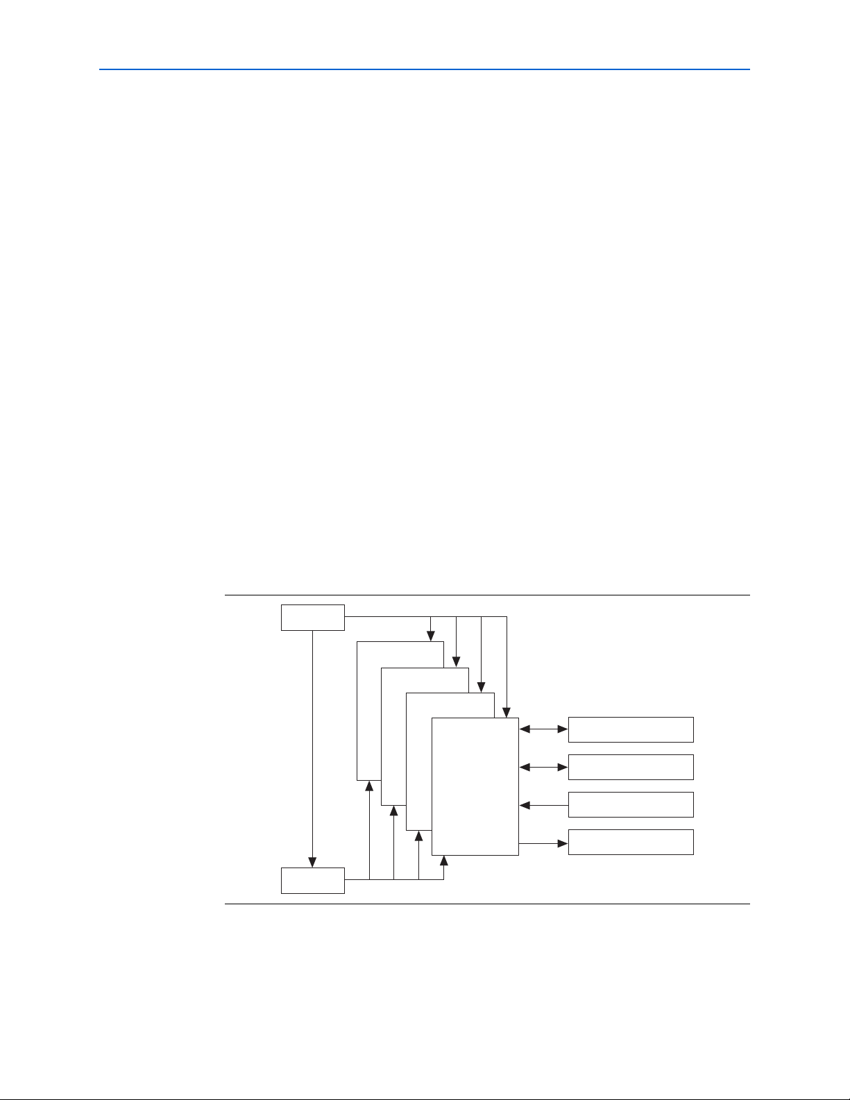
Features
Features
The ALTDLL and ALTDQ_DQS megafunctions offer the following features:
■ ALTDLL
■ A delay-locked loop (DLL) block to center-align the read strobe with read data.
■ Phase offset control blocks to fine-tune the delay time on the read strobe using
static or dynamic offset.
■ ALTDQ_DQS
■ Supports RLDRAM II memory interface.
■ DDR registers on the input and output paths to read or write to an external
DDR interface.
■ Half-rate registers to enable successful data transfers between the I/O registers
and the core logic.
■ Access to dynamic on-chip termination (OCT) controls to switch between
parallel termination during reads to series termination during writes.
■ Access to I/O delay chains to fine-tune delays on the data or strobe signals
statically or dynamically.
Figure 1–1 shows a high-level overview of how you can connect the ALTDQ_DQS
megafunction with other megafunctions such as ALTPLL, ALTDLL, and ALTIOBUF,
to create a full custom external memory interface. Figure 1–1 shows a 36-bit interface
created with ALTDQ_DQS instantiations, where each instantiation is configured in
the ×9 mode.
Figure 1–1. System-Level View
ALTDLL and ALTDQ_DQS Megafunctions User Guide © February 2012 Altera Corporation
Page 7
Design Flow
Build the Datapath
Simulate the Design
Create Timing Constraints
Compile the Design and Verify Timing
Adjust Constraints
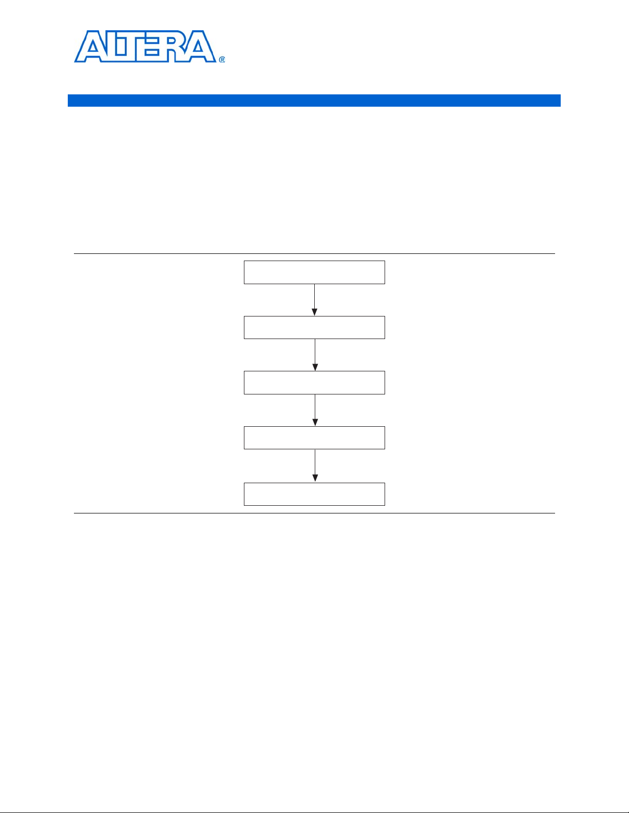
2. Getting Started
This chapter describes the FPGA design flow to implement a custom memory
interface datapath using the ALTDLL and ALTDQ_DQS megafunctions and Altera’s
FPGA hardware features.
Figure 2–1 shows the design flow for creating a custom memory datapath system
with the ALTDLL and ALTDQ_DQS megafunctions and the Quartus
Figure 2–1. Design Flowchart
®
II software.
Build the Datapath
© February 2012 Altera Corporation ALTDLL and ALTDQ_DQS Megafunctions User Guide
After you identify the requirements for your custom external memory interface, the
first stage is to build a datapath to interface with the memory blocks.
To build the datapath, you must perform the following steps:
1. Create a project in the Quartus II software that targets the preferred Altera device.
2. Instantiate the ALTPLL megafunction to provide the required clocking scheme for
the custom PHY.
f For more information about instantiating megafunctions and the clocking
scheme, refer to Instantiate the ALTPLL Megafunction section in volume 5 of
the External Memory Interface Handbook. For more information about using
PLLs, refer to the ALTPLL Megafunction User Guide.
3. Instantiate the ALTDLL megafunction to implement the DLL.
Page 8

Chapter 2: Getting Started 2–2
Design Flow
4. Instantiate the ALTDQ_DQS megafunction to implement the read and write PHY
required for the interface.
5. Integrate the custom PHY with user logic, and a custom or third party memory
controller if needed.
6. Instantiate the ALTIOBUF megafunction to use the I/O buffers for pin
connections. This megafunction enables dynamic OCT capabilities for the
respective interface pins.
f For more information about the pin connections, refer to “ALTIOBUF
Megafunction and Delay Chains Integration” on page 4–18. For more
information about the ALTIOBUF megafunction, refer to I/O Buffer
(ALTIOBUF) Megafunction User Guide.
7. Connect all the instances of ALTPLL, ALTDLL, ALTDQ_DQS, ALTIOBUF, and
other custom memory controllers in the Quartus II software.
The following sections discuss other megafunctions or customized controller logic
that are used in some cases.
ALTOCT Megafunction
If you use the OCT capabilities in the targeted devices, you eliminate the need for
external series or parallel termination resistors, and you simplify the design of a PCB.
If the I/O in your design uses calibrated series, parallel, or dynamic termination, your
design requires a calibration block. This block requires a pair of R
located in a bank that shares the same V
voltage as your memory interface. This
CCIO
calibration block is not required to be in the same bank or side of the device as the I/O
elements it is serving. To use these capabilities in the FPGA, you must turn on the Use
dynamic OCT path option when parameterizing the ALTDQ_DQS megafunction,
and instantiate the ALTOCT megafunction.
and RDN pins
UP
f For more information about the OCT capabilities in the DQ/DQS path, refer to
“DQ/DQS OCT Path” on page 4–14.
Customized Controller Logic
In some cases, you require a customized controller logic to control the PHY created
with the ALTDLL and ALTDQ_DQS instances. You must create a controller logic for
the following instances:
■ Controller logic for data, data_valid, and strobe pins for the custom external
memory interface.
■ If you use calibrated termination, controller logic for all pins in the ALTOCT
instances associated with the custom external memory interface.
f For more information about calibrated termination, refer to Dynamic
Calibrated On-Chip Termination (ALTOCT) Megafunction User Guide.
© February 2012 Altera Corporation ALTDLL and ALTDQ_DQS Megafunctions User Guide
Page 9

2–3 Chapter 2: Getting Started
Design Flow
Simulate the Design
After instantiating the megafunctions, the Quartus II software generates design
source files and Verilog or VHDL simulation model files. Simulate these files in
Modelsim-AE, Modelsim SE, or other third-party functional simulator tools.
f For information about functional and gate-level timing simulations, refer to
Simulating Altera Designs chapter in volume 3 of the Quartus II Handbook.
Create Timing Constraints
The ALTDLL and ALTDQ_DQS megafunctions do not provide automatic timing
scripts for custom external memory interfaces. You must create your own timing
constraints for the following paths and clocks:
■ Timing paths from FPGA I/O to external device.
■ Timing paths from I/O registers to core logic.
■ PLL and other clock constraints.
After creating your constraints, perform the timing analysis using the TimeQuest
timing analyzer in the Quartus II software.
f Because the timing analysis for custom external memory interfaces are the same as the
timing analysis for source-synchronous interfaces, refer to the Timing Analysis section
in volume 3 of the Quartus II Handbook and AN 433: Constraining and Analyzing
Source-Synchronous Interfaces.
The ALTDLL and ALTDQ_DQS custom PHY solution supports timing analysis using
the TimeQuest timing analyzer with Synopsys Design Constraints (SDC)
assignments. You can derive the timing constraints from the external device data
sheet and tolerances from the board layout.
f For more information about timing constraints, refer to “Appendix D: Interface
Timing Analysis” section in AN 328: Interfacing DDR2 SDRAM with Stratix II, Stratix II
GX, and Arria GX Devices.
For more information about creating timing constraints in SDC format for the
TimeQuest timing analyzer, refer to the The Quartus II TimeQuest Timing Analyzer
chapter of the Quartus II Handbook. Depending on which simulation tool you are
using, refer to the appropriate chapter in the Simulation section in volume 3 of the
Quartus II Handbook.
Compile the Design and Verify Timing
After constraining your design, compile your design in the Quartus II software to
generate timing reports to verify whether timing has been met.
After compiling your design in the Quartus II software, run the verifying timing
script to produce the timing report for different paths, such as write data, read data,
address and command, and core (entire interface) timing paths in your design.
ALTDLL and ALTDQ_DQS Megafunctions User Guide © February 2012 Altera Corporation
Page 10

Chapter 2: Getting Started 2–4
Design Example: Implementing Read Paths Using Stratix III Devices
The timing analyzer reports margins on the following paths:
■ Address and command setup and hold margin
■ Half-rate address and command setup and hold margin
■ Core setup and hold margin
■ Core reset and removal setup and hold margin
■ Write setup and hold margin
■ Read capture setup and hold margin
f For more information about timing analysis and reporting using the ALTDLL and
ALTDQ_DQS external memory solution, refer to the Analyzing Timing of Memory IP
chapter in volume 2 of the External Memory Interface Handbook.
Adjust Constraints
The timing report shows the worst case setup and hold margin for the different paths
in your design. If the setup and hold margin do not meet timing requirements, adjust
the phase setting of the clocks that latch the data.
For example, the address and command outputs are clocked by an address and
command clock that may be different than the system clock, which is 0°. The system
clock clocks the clock outputs going to the memory. If the report timing script
indicates that using the default phase setting for the address and command clock
results in more hold time than setup time, adjust the address and command clock to
be less negative than the default phase setting to ensure that there is less hold margin.
Similarly, adjust the address and command clock to be more negative than the default
phase setting if there is more setup margin.
Design Example: Implementing Read Paths Using Stratix III Devices
This section provides a walkthrough of a simple design example. The design example
demonstrates a Stratix III device reading from an external DDR2 SDRAM. The DDR2
external memory interface is implemented using the ALTDLL and ALTDQ_DQS
megafunctions. This design requires 1 DQS and 8 DQ input pins. The DQS frequency
for the design is 150 MHz and the data rate is 300 Mbps.
1 For a more complex design example, refer to “Design Example: Implementing
Half-Rate DDR2 Interface in Stratix III Devices” on page 4–49.
f The design examples are available next to the ALTDLL and ALTDQ_DQS
Megafunctions User Guide on the Documentation: User Guides page of the Altera
website.
© February 2012 Altera Corporation ALTDLL and ALTDQ_DQS Megafunctions User Guide
Page 11
2–5 Chapter 2: Getting Started
Design Example: Implementing Read Paths Using Stratix III Devices
Generate the Megafunctions
Create a Quartus II project and generate the following megafunctions:
■ ALTPLL megafunction
■ ALTDLL megafunction
■ ALTDQ_DQS megafunction
■ ALTIOBUF megafunction
Create a Quartus II Project
Create a project in the Quartus II software that targets the EP3SL150F1152-C2 device
for the DDR2 SDRAM by performing the following steps:
1. Open the altdll_altdq_dqs_DesignExample_ex1.zip file and extract the
altdll_altdq_dqs_design_ex1.qar file.
2. In the Quartus II software, restore the altdll_altdq_dqs_design_ex1.qar file into
your working directory.
3. Open the altdll_altdq_dqs_design_ex1.bdf file.
Generate the ALTPLL Megafunction
Before generating the ALTDLL and ALTDQ_DQS megafunctions, you must generate
the ALTPLL megafunction first by performing the following steps:
1. Double-click anywhere on the Block Editor window. The Symbol window appears.
2. Click MegaWizard Plug-In Manager. Page 1 of the MegaWizard
Manager appears.
3. Select Create a new custom megafunction variation.
4. Click Next. Page 2a of the MegaWizard Plug-In Manager appears.
5. Select Create a new custom megafunction variation.
6. Click Next. Page 2a of the MegaWizard Plug-In Manager appears. Select ALTPLL,
and Ver ilo g HD L, and type the file name as PLL_50MHz.v.
7. On the Parameter Settings tab, on the General/Modes page, specify the
parameters as shown in Tab le 2 –1 . These parameters configure the general
settings for the ALTPLL instance.
Table 2–1. ALTPLL Parameter Settings
Settings Value
Currently selected device family Stratix III
Match project/default Turned on.
What is the frequency of the inclock0 input? 50 MHz
How will the PLL outputs be generated? With no compensation
This option is selected because the PLL is
used to clock the ALTDLL instance only.
™
Plug-In
ALTDLL and ALTDQ_DQS Megafunctions User Guide © February 2012 Altera Corporation
Page 12
Chapter 2: Getting Started 2–6
Design Example: Implementing Read Paths Using Stratix III Devices
8. On the Output Clocks tab, on the clk c0 page, specify the parameters as shown in
Tab le 2 –2 . You don’t have to parameterize the other pages on the Output Clocks
tab because you only use one clock for this design.
Table 2–2. ALTPLL Output Clocks/clk c0 Settings
Settings Value
Use this clock Turned on
Enter output clock frequency 150 Mhz
Clock phase shift 0 deg
Clock duty cycle (%) 50
9. Click Finish.
10. Click Finish. The ALTPLL instance is generated.
11. Click OK to close the Symbol window.
12. Place the instance on the altdll_altdq_dqs_design_ex1.bdf Block Editor.
Generate the ALTDLL Megafunction
To generate the ALTDLL megafunction, perform the following steps:
1. Double-click anywhere on the Block Editor window. The Symbol window appears.
2. Click MegaWizard Plug-In Manager. Page 1 of the MegaWizard Plug-In Manager
appears.
3. Select Create a new custom megafunction variation.
4. Click Next. Page 2a of the MegaWizard Plug-In Manager appears.
5. Select Create a new custom megafunction variation.
6. Click Next. Page 2a of the MegaWizard Plug-In Manager appears. Select ALTDLL,
and Ver ilo g HD L, and type the file name as dll_150MHz.v.
7. On the Parameter Settings tab, on the General page, specify the parameters as
shown in Tabl e 2– 3. These parameters configure the general settings for the
ALTDLL instance.
Table 2–3. ALTDLL GeneraL Settings
Settings Value
Currently selected device family Stratix III
Match project/default Turned on.
Number of Delay Chains 12
Refer to Stratix III Device Datasheet: DC and
Switching Characteristics of Stratix III Devices
chapter in the Stratix III Device Handbook, and
pick a DLL mode that supports 150 MHz and
find the DLL setting.
© February 2012 Altera Corporation ALTDLL and ALTDQ_DQS Megafunctions User Guide
Page 13
2–7 Chapter 2: Getting Started
Table 2–3. ALTDLL GeneraL Settings
Settings Value
DQS Delay Buffer Mode Low
Input Clock Frequency 150 MHz
Turn on jitter reduction Turned off.
Design Example: Implementing Read Paths Using Stratix III Devices
Refer to Stratix III Device Datasheet: DC and
Switching Characteristics of Stratix III Devices
chapter in the Stratix III Device Handbook, and
pick a DLL mode that supports 150 MHz and
find the DLL setting.
8. On the DLL Offset Controls/Optional Ports page, specify the parameters as
shown in Tabl e 2– 4.
Table 2–4. ALTDLL Parameter Settings/DLL Offset Controls/Optional Ports Settings
Settings Value
DLL Phase Offset Control A
Instantiate dll_offset_ctrl block
DLL Phase Offset Control B
Instantiate dll_offset_ctrl block
Optional Ports
Create a dll_aload port
Optional Ports
Create a dll_dqsupdate port
Turned off.
The design is intended to run slow, so you do
not need to select this parameter. However, if
the read timing is unbalanced, you can
fine-tune the DQS phase shift using this
parameter.
Turned off.
Turned off.
Turned off.
9. Click Finish.
10. Click Finish. The ALTDLL instance is generated.
11. Click OK to close the Symbol window.
12. Place the instance on the Block Editor.
Generate the ALTDQ_DQS Megafunction
To generate the ALTDQ_DQS megafunction, perform the following steps:
1. Double-click anywhere on the Block Editor window. The Symbol window appears.
2. Click MegaWizard Plug-In Manager. Page 1 of the MegaWizard Plug-In Manager
appears.
3. Select Create a new custom megafunction variation.
4. Click Next. Page 2a of the MegaWizard Plug-In Manager appears. Select
ALTDQ_DQS, and Verilog HDL, and type the file name as dq_dqs_input_path.v.
5. On the Parameter Settings page, specify the parameters as shown in Ta bl e 2– 5.
These parameters configure the general settings for the ALTDQ_DQS instance.
ALTDLL and ALTDQ_DQS Megafunctions User Guide © February 2012 Altera Corporation
Page 14
Chapter 2: Getting Started 2–8
Design Example: Implementing Read Paths Using Stratix III Devices
.
Table 2–5. Parameter Settings
Parameter Value
RLDRAMII Mode NONE
Number of bidirectional DQ 0
Number of input DQ 8
Number of output DQ 0
Number of stages in dqs_delay_chain 3
DQS input frequency 150 MHz
Use half-rate components Turned off.
The design uses full-rate
memory components, so
you do not select this
option.
Use Dynamic OCT Turned off.
Dynamic OCT is not used for
input paths.
Add memory interface specific fitter grouping assignments Turned on.
6. On the Advanced Options tab, on the DQS IN page, specify the parameters as
shown in Tabl e 2– 6. These parameters configure the DQS input path of the
ALTDQ_DQS instance.
Table 2–6. Advance Options (DQS IN)
Parameter Sub-options Value
Enable DQS Input Path — Turned on.
Enable dqs_delay_chain —Selected.
Advanced delay chain options Select dynamically using
Turned off.
configuration registers
DQS delay chain
‘delayctrlin’ port source
DLL
The DQS delay-chain settings
is based on the DLL.
DQS Delay Buffer Mode Low
Use the same mode selected
in the DLL settings.
DQS Phase Shift 9000..
Specify a 90° DQS phase shift.
The phase-shift value must
inter-relate with the selected
dqs_delay_chain stage.
Enable DQS offset control Turned off.
Disable DQS delay fine-tuning
using offset feature.
Enable DQS delay chain
Turned off.
latches
© February 2012 Altera Corporation ALTDLL and ALTDQ_DQS Megafunctions User Guide
Page 15
2–9 Chapter 2: Getting Started
Table 2–6. Advance Options (DQS IN)
Parameter Sub-options Value
Enable DQS busout delay chain — Turned on.
Enable DQS enable block — Turned on.
Design Example: Implementing Read Paths Using Stratix III Devices
7. On the DQS OUT/OE page, turn off the Enable DQS output path option. When
you deselect the Enable DQS output path option, the other options on this page
are disabled.
8. On the DQ IN page, specify the parameters as shown in Tabl e 2– 7. These
parameters configure the DQ input path of the ALTDQ_DQS instance.
Table 2–7. Advance Options (DQ IN)
Options Value
DQ input register mode DDIO
Select DDIO to enable double data rate capture for
DQ.
DQ input register clock source dqs_bus_out port and turn off Connect DDIO clkn to
DQS_BUS from complementary DQSn
Use DQ input phase alignment Turned off.
The feature is for half-rate components; the design
uses full-rate memory components.
Use DQ input delay chain Turned on.
9. On the DQ OUT/OE page, all the options are automatically disabled because the
design is not using output DQ. The parameters on this page configure the DQ
output and OE paths of the ALTDQ_DQS instance.
10. On the Half-rate page, for the IO Clock Divider Invert Phase parameter, turn on
Never because the design requires full-rate components. The other options are
automatically disabled. The parameters on this page configure the half-rate
settings of the ALTDQ_DQS instance.
11. On the OCT Path page, all the options are automatically disabled because the
design is not using input and output DQS or bidirectional DQ. The parameters on
this page configure the OCT path of the ALTDQ_DQS instance.
12. On the DQSn I/O page, turn off the Use DQSn I/O option because the design is
not using DQSn. When you turn off the Use DQSn I/O option, the other options
on this page are disabled.
13. In the Reset/Config Ports tab, tun off all the parameters.
14. Click Finish.
15. Click Finish. The ALTDQ_DQS instance is generated.
16. Click OK to close the Symbol window.
17. Place the instance on the Block Editor.
ALTDLL and ALTDQ_DQS Megafunctions User Guide © February 2012 Altera Corporation
Page 16
Chapter 2: Getting Started 2–10
Design Example: Implementing Read Paths Using Stratix III Devices
Generate the ALTIOBUF Megafunction
You must generate the ALTIOBUF megafunction to set the following I/O buffer
settings:
■ 1 input buffer for input DQS pin
■ 8 input buffers for input DQ pins
To generate the ALTIOBUF megafunction, perform the following steps:
1. Double-click anywhere on the Block Editor window. The Symbol window appears.
2. Click MegaWizard Plug-In Manager. Page 1 of the MegaWizard Plug-In Manager
appears.
3. Select Create a new custom megafunction variation.
4. Click Next. Page 2a of the MegaWizard Plug-In Manager appears. Select
ALTIOBUF, and Ver ilo g HD L, and type the file name as ibuf_input_dqs.v (for
DQS pin) or ibuf_input_dq.v (for DQ pins).
5. On the Parameter Settings page, specify the parameters as shown in Ta bl e 2– 8.
These parameters configure the general settings for the ALTIOBUF instance.
Table 2–8. ALTIOBUF General Settings
Value
Settings
1 input buffer for the
input DQS pins
8 input buffer for the
input DQ pins
Currently selected device family Stratix III Stratix III
How do you want to configure this module? As an input buffer As an input buffer
What is the number of buffers to be
18
instantiated?
Use bus hold circuitry Turned off. Turned off.
Use differential mode Turned off. Turned on.
Use open drain output Turned off. Turned off.
Use output enable port Turned off. Turned off.
Use dynamic termination control Turned off. Turned off.
Use series and parallel termination control Turned off. Turned off.
6. On the Dynamic Delay Chains page, specify the parameters as shown in
Tab le 2 –9 .
Table 2–9. ALTIOBUF Dynamic Delay Chain Settings
Value
Settings
1 input buffer for the
input DQS pins
8 input buffer for the
input DQ pins
Enable input buffer dynamic delay chain Turned off. Turned off.
Enable output buffer dynamic delay chain 1 Turned off. Turned off.
Enable output buffer dynamic delay chain 2 Turned off. Turned off.
Create a ‘clkena’ port Turned off Turned off.
© February 2012 Altera Corporation ALTDLL and ALTDQ_DQS Megafunctions User Guide
Page 17
Chapter 2: Getting Started 2–11
© February 2012 Altera Corporation ALTDLL and ALTDQ_DQS Megafunctions User Guide
7. Click Finish.
Design Example: Implementing Read Paths Using Stratix III Devices
8. Click Finish. The ALTIOBUF instance is generated.
9. Click OK to close the Symbol window.
10. Place the instance on the Block Editor.
f For more information about connecting all the instances, refer to “Integrate the I/O Buffer Modules with the
ALTDQ_DQS modules” on page 4–55.
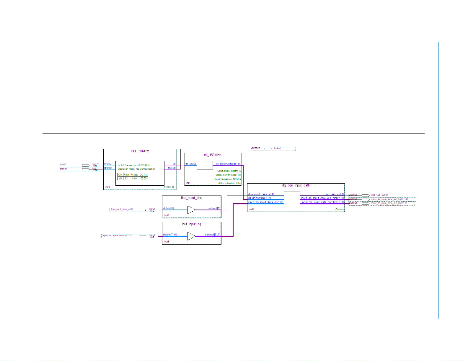
11. On the Block Editor, connect all the instances as shown in Figure 2–2 on page 2–11.
Figure 2–2. Block Diagram of the Design Example
Page 18

2–12 Chapter 2: Getting Started
Design Example: Implementing Read Paths Using Stratix III Devices
Compile and Simulate the Design
On the Processing menu, click Start Compilation to compile the design. After the
design is compiled, you can view the implemention in the RTL Viewer. You can also
view the resource usage in the Compilation Report.
After you compile your design, simulate the design in the ModelSim-Altera software
to generate a waveform display of the device behavior. Set up and simulate the design
in the ModelSim-Altera software by performing the following steps:
1. Unzip the altdll_altdq_dqs_ex1_msim.zip file to your preferred working
directory on your PC.
2. Start the ModelSim-Altera software.
3. On the File menu, click Change Directory.
4. Select the folder in which you unzipped the files in the
altdll_altdq_dqs_ex1_msim.zip folder.
5. Click OK.
6. On the Tools menu, point to Tc l and click Execute Macro.
7. Select the altdll_altdq_dqs_ex1_msim.do file and click Open. This is a script file
for the ModelSim-Altera software to automate all the necessary settings for the
simulation.
8. Verify the results with the simulation waveform.
1 You can rearrange, remove and add signals, and change the radix by
modifying the script in the altdll_altdq_dqs_ex1_msim.do file.
ALTDLL and ALTDQ_DQS Megafunctions User Guide © February 2012 Altera Corporation
Page 19

The Quartus II software provides the MegaWizard Plug-In Manager that helps you
quickly customize your megafunction variation. The parameter editor provides a list
of megafunctions and available options for each variation.
Altera recommends that you use the parameter editor to instantiate the ALTDLL and
ALTDQ_DQS megafunctions. However, for advanced users, if you want to bypass the
MegaWizard Plug-In Manager and use the megafunctions as directly parameterized
instantiations in your design, you can use the clear box generator. For more
information about the clear box generator, refer to Appendix A, Clear Box Generator.
1 Some advanced parameters can only be modified through the clear box parameters.
ALTDLL Parameter Editor
This section provides information about the ALTDLL MegaWizard parameters.
3. Parameter Settings
1 For advanced users who may use the clearbox generator, the clearbox parameter
names are provided for the corresponding MegaWizard parameters.
The ALTDLL Parameter Settings page in the ALTDLL parameter editor allows you to
configure the parameters in the following pages:
■ General
■ DLL Offset Controls/Optional Ports
Tab le 3 –1 shows the options available on the General page.
© February 2012 Altera Corporation ALTDLL and ALTDQ_DQS Megafunctions User Guide
Page 20

3–2 Chapter 3: Parameter Settings
ALTDLL Parameter Editor
Table 3–1. Options on General Settings Page
Clear Box
Parameter Name Legal Value
Number of Delay
Chains
6, 8, 10, 12,
or 16
Parameter Name Description
DELAY_CHAIN_
LENGTH
Represents the number of delay buffers in the delay loop.
The DLL consists of 6, 8, 10, 12, or 16 DLL-controlled
delay buffers chained together. The total delay in the DLL
delay chain is computed with the following equation:
delay = delay_chain_length
x delay_buffer_delay
The DLL uses the delay chain to implement a 360° phase
shift. By comparing the incoming clock to the 360°-shifted
clock, the DLL determines the delay setting to implement
an actual 360° phase shift in its delay chain. Because each
delay buffer is identical, each buffer in the delay chain
implements a phase shift that is equal to
(360/delay_chain_length)°.
The default value is 12.
DQS Delay Buffer
Mode
Low or High DELAY_BUFFER_
MODE
Specifies the frequency mode for the variable delay
buffers.
If you select Low, the
dll_offset_ctrl_a_offsetctrlout [5..0]
or dll_offset_ctrl_b_offsetctrlout
[5..0] output is limited to a maximum value of 63.
If you select High, the output is limited to a maximum value
of 31.
The default value is Low.
Input Clock
Frequency
INPUT_FREQUENCY Specifies the frequency of the clock (in MHz) that is
connected to the clk input port. This frequency must be
within the valid range for the device you are using. You can
specify a duration in ps. The value is in floating-point
format with no decimal point limit.
The default value is 300 MHz.
For information about the clock range for the Altera
devices, refer to the respective device handbook.
Turn on jitter
reduction
— JITTER_REDUCTION Enables the jitter reduction circuit. Jitter affects the signal
integrity of the clock signal from a PLL clock source or an
external clock pin. If you turn on this parameter, the jitter
reduction circuit is enabled on the
dll_delayctrlout[5..0] and
dll_offset_ctrl_a_offsetctrlout [5..0],
or the dll_offset_ctrl_b_offsetctrlout
[5..0] output port.
When the jitter reduction circuit is enabled, the DLL may
require up to 1,024 clock cycles to lock. When the jitter
reduction circuit is disabled, the DLL requires only up to
256 clock cycles to lock.
ALTDLL and ALTDQ_DQS Megafunctions User Guide © February 2012 Altera Corporation
Page 21

Chapter 3: Parameter Settings 3–3
ALTDLL Parameter Editor
The DLL Offset Controls/Optional Ports page allows you to instantiate the DLL
offset control blocks (A and B), specify whether to use static offset, and create the
dll_aload and dll_dqsupdate optional ports. Tab le 3– 2 shows the options
available on DLL Offset Controls/Optional Ports page.
.
Table 3–2. Options on DLL Offset Controls/Optional Ports Page (Part 1 of 2)
Clear Box
Parameter Name Legal Value
DLL Phase Offset
Control A
Instantiate
dll_offset_ctrl
block
Set statically
to
or
Set
dynamically
Parameter Name Description
USE_DLL_OFFSET_
CTRL_A
Instantiates DLL_OFFSET_CTRL_A block. The block
can be placed either at the top, bottom, or side of the
FPGA device, depending on how the Quartus II Fitter
places it. If you turn on this parameter, you must
specify whether you want to set the blocks statically or
dynamically.
using offset
input port
–63 to 63 DLL_OFFSET_CTRL_A_
STATIC_OFFSET
The Set statically to option is a signed integer. Turn on
this option if you want a fixed offset value, and key in
the value you want.
This fixed value is added to the DLL feedback counter
and the output is generated on the
dll_offset_ctrl_a_offsetctrlout
[5..0]output port.
The default value is 0.
— DLL_OFFSET_CTRL_A_
USE_OFFSET
The Set dynamically using offset input port option
determines the output of the
dll_offset_ctrl_a_offsetctrlout
[5..0] output port. Turn on this option if you want a
dynamic offset value.
If you turn on this option, depending on whether the
dll_offset_ctrl_a_addnsub signal is
asserted or not, the phase offset specified on the offset
input bus is added or subtracted from the DLL feedback
counter output to get the
dll_offset_ctrl_a_offsetctrlout
[5..0]output.
© February 2012 Altera Corporation ALTDLL and ALTDQ_DQS Megafunctions User Guide
Page 22

3–4 Chapter 3: Parameter Settings
ALTDLL Parameter Editor
Table 3–2. Options on DLL Offset Controls/Optional Ports Page (Part 2 of 2)
Clear Box
Parameter Name Legal Value
DLL Phase Offset
Control B
Instantiate dll
offset_ctrl block
Set statically
to
or
Set
dynamically
using offset
Parameter Name Description
USE_DLL_OFFSET_
CTRL_B
Instantiates DLL_OFFSET_CTRL_B block. The block
can be placed either at the top, bottom, or side of the
FPGA device, depending on how the Quartus II Fitter
places it.
If you turn on this option, you must specify whether
you want to set the blocks statically or dynamically.
input port
–63 to 63 DLL_OFFSET_CTRL_B_
STATIC_OFFSET
The Set statically to option is a signed integer.
Turn on this option if you want a fixed offset value, and
key in the value you want.
This fixed value is added to the DLL feedback counter
and the output is generated on the
dll_offset_ctrl_b_offsetctrlout[5..0
]output port.
The default value is 0.
— DLL_OFFSET_CTRL_B_
USE_OFFSET
The Set dynamically using offset input port option
determines the output of the
dll_offset_ctrl_b_offsetctrlout
[5..0] output bus. Turn on this option if you want a
dynamic offset value.
If you turn on this option, depending on whether the
dll_offset_ctrl_b_addnsub signal is
asserted or not, the phase offset specified on the offset
input bus is added or subtracted from the DLL feedback
counter output to get the
dll_offset_ctrl_b_offsetctrlout
[5..0]output.
Optional Ports
Create a
dll_aload
port
— DLL_ALOAD Enables the asynchronous-load signal for the DLL up or
down counter. When the dll_aload signal is high,
the counter is asynchronously loaded with the initial
delay setting of 16 in low-frequency mode when you
select Low for the DQS Delay Buffer Mode parameter,
or 32 in high-frequency mode when you select High for
the DQS Delay Buffer Mode parameter. This input
defaults to GND.
Optional Ports
Create a
‘dll_dqsupdate’
port
— DLL_DQSUPDATE Enables the update-enable signal for the delay-setting
latches in the DQS pins. This signal only feeds the
dqsupdateen port of the ALTDQ_DQS
megafunction.
To use the dll_dqsupdate signal, you must turn on
the Enable DQS delay chain latches option on the
DQS IN page in the ALTDQ_DQS parameter editor.
The Simulation Model page allows you to optionally generate simulation model files.
The Summary page displays a list of the types of files to be generated. The
automatically generated variation file contains wrapper code in the language you
specified earlier. On this page, you can specify additional types of files to be
generated.
ALTDLL and ALTDQ_DQS Megafunctions User Guide © February 2012 Altera Corporation
Page 23

Chapter 3: Parameter Settings 3–5
ALTDQ_DQS Parameter Editor
Choose from the following file types:
■ Quartus II IP file (<function name>.qip)
■ Instantiation template file (<function name>.v)
■ Verilog HDL black box file (<function name>_bb.v)
■ AHDL Include file (<function name>.inc)
■ VHDL component declaration file (<function name>.cmp)
■ Quartus II symbol file (<function name>.bsf)
If you select Generate netlist on the Simulation Model page, the file for that netlist is
also available. A gray checkmark indicates a file that is automatically generated, and a
green checkmark indicates generation of an optional file
ALTDQ_DQS Parameter Editor
This section provides information about the ALTDQ_DQS MegaWizard parameters.
1 For advanced users who may use the clearbox generator, the clearbox parameter
names are provided for the corresponding MegaWizard parameters.
The Parameter Settings page in the ALTDQ_DQS parameter editor allows you to
configure the parameters in Tab le 3 –3 .
© February 2012 Altera Corporation ALTDLL and ALTDQ_DQS Megafunctions User Guide
Page 24

3–6 Chapter 3: Parameter Settings
.
ALTDQ_DQS Parameter Editor
Table 3–3. Options on Parameter Settings Page (Part 1 of 2)
Clear Box
Parameter Name Legal Value
RLDRAMII mode NONE, x9,
x18, or x36
Parameter Name Description
RLDRAMII_MODE Enables RLDRAM II support for ALTDQ_DQS instance.
If you select x9 or x18 mode, the DK pins do not have
group assignments, but they must be placed in the same
bank or chip edge as the other pins in the interface. If you
select x36 mode, the DK/DK# pins must be placed
manually in DQS locations.
If you select x18 mode, place the DM pins in either group
0 or group 1, which forces QVLD to the other group. If you
select x36 mode, place the DM pins in group 0 or 1, and
QVLD to be in group 0 or 1.
All combinations are allowed. Not supported in Arria II GX.
Data mask pin
group
NONE,
GROUP0, or
GROUP1
DM_LOC Specifies the group assignment for the DM pin group.
If you select NONE for the RLDRAMII mode option, then
this option defaults to NONE.
If you select x9 for the RLDRAMII mode option, then this
option defaults to NONE.
If you select x18 for the RLDRAMII mode option, then for
this option you can select either NONE, GROUP0, or
GROUP1. If you select GROUP0, then GROUP1 is used for
the Q valid signal group option, and if you select
GROUP1, then GROUP0 is used for the Q valid signal
group option.
If you select x36 for the RLDRAMII mode option, then for
this option you can select either NONE, GROUP0, or
G
ROUP1.
Not supported in Arria II GX devices.
Q valid signal
group
NONE,
GROUP0, or
GROUP1
QVLD_LOC Specifies the group assignment for the Q valid signal
group.
If you select NONE for the RLDRAMII mode option, then
this option defaults to NONE.
If you select x9 for the RLDRAMII mode option, then this
option defaults to GROUP0.
If you select x18 for the RLDRAMII mode option, then this
option depends on the Data mask pin group option. If you
select GROUP0 for the Data mask pin group option, then
GROUP1 is defaulted for this option, and if you select
GROUP1 for the Data mask pin group option, then
GROUP0 is defaulted for this option.
If you select x36 for the RLDRAMII mode option, then for
this option you can select either NONE, GROUP0, or
GROUP1.
Not supported in Arria II GX devices.
Number of
bidirectional DQ
0–48 NUMBER_OF_
BIDIR_DQ
Specifies the number of bidirectional DQ ports used in the
ALTDQ_DQS instance.
ALTDLL and ALTDQ_DQS Megafunctions User Guide © February 2012 Altera Corporation
Page 25

Chapter 3: Parameter Settings 3–7
ALTDQ_DQS Parameter Editor
Table 3–3. Options on Parameter Settings Page (Part 2 of 2)
Clear Box
Parameter Name Legal Value
Number of input
0–48 NUMBER_OF_
DQ
Number of output
0–48 NUMBER_OF_
DQ
Number of stages
1, 2, 3, and 4 DQS_DELAY_CHAIN_
in
dqs_delay_chain
Parameter Name Description
Specifies the number of input DQ ports used in the
INPUT_DQ
ALTDQ_DQS instance.
Specifies the number of output DQ ports used in the
OUTPUT_DQ
ALTDQ_DQS instance.
Specifies the stages of DQS_DELAY_CHAIN. The
PHASE_SETTING
number of stages depends on the intended phase shift
that you want to clock for <IO>_DDIO_IN block in the
DQ input path. The bigger the value you specify, the longer
the delay.
The coarse phase shift depends on this option. For
example, in Stratix IV devices, if you set the frequency
mode to 1, you will get a phase shift of 20°, 60°, 90°, or
120°. If you set Number of stages in dqs_delay_chain
value to 2, you will get 60° phase shift and if you set the
Number of stages in dqs_delay_chain value to 1, you will
get 30° phase shift.
DQS input
frequency
— DQS_INPUT_
FREQUENCY
Specifies the input frequency of the DQS strobe in MHz.
The input frequency must match the DLL (ALTDLL) input
frequency.
Use half rate
components
— USE_HALF_RATE Instantiates the half-rate blocks in the ALTDQ_DQS
instance. This parameter is used only when the external
memory interface requires half-rate mode.
Not supported in Arria II GX devices.
Use dynamic OCT
path
— USE_DYNAMIC_OCT Instantiates the dynamic OCT blocks in the ALTDQ_DQS
instance. This parameter enables access to dynamic OCT
paths on both DQ and DQS paths. The dynamic OCT
features enable parallel termination (R
the external memory and disable R
) during reads from
t
during writes to the
t
external memory.
Not supported in Arria II GX devices.
Add memory
interface specific
fitter grouping
— ADD_MEM_FITTER_
GROUP_ASSIGNMENTS
Enables the Quartus II Fitter to automatically assign the
memory interface I/O ports to the memory interface I/O
pins on the FPGA.
assignments
The Advanced Options page allows you to configure the parameters in the following
pages:
■ DQS IN
■ DQS OUT/OE
■ DQ IN
■ DQ OUT/OE
■ Half-rate
■ OCT Path
■ DQSn I/O
© February 2012 Altera Corporation ALTDLL and ALTDQ_DQS Megafunctions User Guide
Page 26

3–8 Chapter 3: Parameter Settings
■ Reset/Config Ports
ALTDQ_DQS Parameter Editor
Tab le 3 –4 describes the options available on the DQS IN page. This page allows you
to configure the DQS input path. For more information about the DQS input path,
refer to “DQS Input Path” on page 4–6.
Table 3–4. Options on DQS IN Page (Part 1 of 3)
Clear Box
Parameter Name Legal Value
Enable DQS Input
—
Path
Enable DQS Input
—
Path
Delay chain
— USE_DQS_INPUT_
usage:
Enable dynamic
delay chain
Parameter Name Description
USE_DQS_INPUT_PATH
USE_DQS_INPUT_PATH
Instantiates the DQS input path.
Instantiates the DQS input path.
Enables <IO>_INPUT_DELAY_CHAIN (D1) on the
DELAY_CHAIN
DQS input path. If you turn on this parameter,
DQS_DELAY_CHAIN block in the path is disabled. D1
is a run-time adjustable delay chain.
To configure delay chains dynamically, refer to “Delay
Chains” on page 4–15.
Delay chain
usage:
Enable
— USE_DQS_DELAY_
CHAIN
Enables DQS_DELAY_CHAIN block. The DQS delay
chain is a DLL-controlled delay chain used to phase shift
the DQS read clock.
dqs_delay_chain
Enable DQS
busout delay
chain
— USE_DQSBUSOUT_
DELAY_CHAIN
Enables DQSBUSOUT_DELAY_CHAIN (Da). This
busout delay chain fine-tunes the outputs of
DQS_DELAY_CHAIN block so that the DQS strobe
timing matches the DQS enable signal. The DQS strobe
has 15 steppable delays, with each step having 50 ps of
delay. Da is a run-time adjustable delay chain.
Enable DQS
enable block
— USE_DQS_ENABLE Enables DQS_ENABLE block. This block grounds the
DQS input strobe when the strobe goes to high
impedance state (Z) after a DDR read postamble.
Enable DQS
enable control
block
— USE_DQS_ENABLE_
CTRL
Enables DQS_ENABLE_CTRL block that controls a
DQS enable circuitry.
You must determine an efficient working
resync_postamble_clk clock phase which clocks
this block to ensure smooth data transfer. The
ALTDQ_DQS megafunction cannot determine the phase
for the data transfer.
Use round trip delay (RTD) analysis or create a custom
data training circuitry to write and read back a training
pattern to and from the memory device and then
dynamically adjust the PLL’s resyncronization clock
phase to find an efficient working phase.
Even though this block controls the DQS enable signal,
the megafunction does not consider the necessary
timing for this signal. Refer to the external memory
interface requirements for the necessary timing.
ALTDLL and ALTDQ_DQS Megafunctions User Guide © February 2012 Altera Corporation
Page 27

Chapter 3: Parameter Settings 3–9
ALTDQ_DQS Parameter Editor
Table 3–4. Options on DQS IN Page (Part 2 of 3)
Clear Box
Parameter Name Legal Value
Enable DQS
— — Enables DQS_ENABLE_DELAY_CHAIN (Db) that
enable block
delay chain
Parameter Name Description
fine-tunes the outputs of DQS_ENABLE_CTRL block
so that the DQS enable signal timing matches the DQS
strobe. Db is a run-time adjustable delay chain.
Advanced Delay
Chain Options
Set dynamically
using
configuration
registers
Advanced Delay
Chain Options
DQS delay chain
delayctrlin port
source
— USE_DQS_DELAY_
CHAIN_PHASECTRLIN
DLL or Core DQS_DELAY_CHAIN_
DELAYCTRLIN_SOURCE
Determines the phasectrlin input for the phase
setting. If you turn on this option, it dynamically chooses
the phase applied to the dqsbusout output during the
FPGA run time. If you turn off this option, the phase
setting is determined by the Number of stages in
dqs_delay_chain option in the Parameter Settings
page. This delay chain fine-tunes the DQS strobe signal.
Determines whether you want the delayctrlin port
to be controlled by DLL (outputs) or from the Core
(FPGA).
If you select DLL, the dll_delayctrlin[5..0]
port is connected to the
dll_delayctrlout[5..0] port of the DLL. The
DLL option adjusts the delay setting in
DQS_DELAY_CHAIN block across pressure, volume,
and temperature (PVT). Altera recommends that you
always select DLL to optimize the read capture at the DQ
input register. If you select Core, the
core_delayctrlin port is fed by the core.
Advanced Delay
Chain Options
DQS Delay Buffer
Mode
Low or High DELAY_BUFFER_MODE Specifies whether the variable delay buffers in the
DQS_DELAY_CHAIN work in low-frequency or
high-frequency mode. The frequency mode must match
the frequency mode you select for the DQS Delay Buffer
Mode parameter on the Parameter Settings page in the
ALTDLL parameter editor.
Advanced Delay
Chain Options
DQS Phase Shift
0–36,000 DQS_PHASE_SHIFT Specifies the phase shift between the delayed DQS signal
and the input DQS signal in units of hundreds of degrees,
for example, a 90° phase shift is represented as 9,000.
Use this parameter for static timing analysis only
be
cause timing analysis cannot determine the phase
shift through the delayctrlin[5..0],
phasectrlin[2..0], and
offsetctrlin[5..0] ports on the megafunction
the way a simulation can. This is an optional field and
defaults to 0.
Advanced Delay
Chain Options
Enable DQS
offset control
— DQS_OFFSETCTRL_
ENABLE
Enables offset values to be added to
DQS_DELAY_CHAIN block. If you turn on this option,
make sure that the ALTDLL instance is set to use the DLL
offset control blocks. This option connects the outputs
from the DLL offset control blocks to the DQS delay
chain block. This parameter is optional and turned off by
default.
© February 2012 Altera Corporation ALTDLL and ALTDQ_DQS Megafunctions User Guide
Page 28

3–10 Chapter 3: Parameter Settings
ALTDQ_DQS Parameter Editor
Table 3–4. Options on DQS IN Page (Part 3 of 3)
Clear Box
Parameter Name Legal Value
Advanced Delay
— DQS_CTRL_LATCHES_
Chain Options
Enable DQS
delay chain
latches
Parameter Name Description
Enables the delayctrlin[5..0] and
ENABLE
offsetctrlin[5..0] inputs to be registered by
the dqsupdateen signal. The DLL continues changing
its delay settings value due to the feedback system.
These DLL values are propagated through the
delayctrlout and offsetctrlout signals of
the DLL and DLL offset control blocks to
DQS_DELAY_CHAIN block to calibrate the necessary
delay settings. These values are updated based on the
dll_dqsupdate port from the DLL, which is
connected to the dqsupdateen port. To use this
option, you must turn on the Create a ‘use
dll_dqsupdate’ port option on the DLL Offset
Controls/Optional Ports page in the ALTDLL parameter
editor.
Advanced Enable
Control Options
DQS Enable
Control Phase
Setting
Set statically
to
or
Set
dynamically
using
configuration
DQS_ENABLE_CTRL_
PHASE_SETTING
If you turn on the Set statically to option, you can select
the phase setting for the delay chains from 0 up to 4 to
fine-tune the DQS enable signal.
If you turn on the Select dynamically using
configuration registers option, the phase setting is
determined by the phasectrlin input for the delay
chains.
registers
Advanced Enable
Control Options
DQS Enable
Control Invert
Phase
Always,
Never, or
Based on
configuration
registers
DQS_ENABLE_CTRL_
INVERT_PHASE
If you turn on Always, the phase output is inverted.
If you turn on Never, the phase output is not inverted.
If you turn on Based on configuration registers, the
phaseinvertctrl input determines whether or not
the inverter is used. The inverter can be used to increase
the number of available phases. This is an optional field
and defaults to Never.
Enable DQS
enable block
delay chain
— USE_DQSENABLE_
DELAY_CHAIN
Enables DQS_ENABLE_DELAY_CHAIN
ch
ain fine-tunes the outputs of DQS_ENABLE_CTRL
block so that the DQS enable signal timing matches the
. This delay
DQS strobe. This delay chain is a run-time adjustable
delay chain.
Tab le 3 –5 describes options available on the DQS OUT/OE page. This page allows
you to configure the DQS output and output enable (OE) paths. For more information
about the DQS output and OE paths, refer to “DQS Output/OE Path” on page 4–12.
Table 3–5. Options on DQS OUT/OE Page (Part 1 of 2)
Clear Box
Parameter Name Legal Value
Enable DQS
— USE_DQS_OUTPUT_
output path
Enable DQS
— USE_DQS_OUTPUT_
output path
ALTDLL and ALTDQ_DQS Megafunctions User Guide © February 2012 Altera Corporation
Parameter Name Description
Instantiates the DQS output path.
PATH
Instantiates the DQS output path.
PATH
Page 29

Chapter 3: Parameter Settings 3–11
ALTDQ_DQS Parameter Editor
Table 3–5. Options on DQS OUT/OE Page (Part 2 of 2)
Clear Box
Parameter Name Legal Value
DQS Output Path
— USE_DQS_OUTPUT_
Options
Enable DQS
output delay
Parameter Name Description
Enables DQS_OUTPUT_DELAY_CHAIN1 (D5) in the
DELAY_CHAIN1
DQS output path. This parameter is used for deskew
purposes or SSN reduction.
D5 is a run-time adjustable delay chain.
chain1
DQS Output Path
Options
Enable DQS
output delay
— USE_DQS_OUTPUT_
DELAY_CHAIN2
Enables DQS_OUTPUT_DELAY_CHAIN2 (D6) in the
DQS output path. This parameter is used for deskew
purposes or SSN reduction.
D6 is a run-time adjustable delay chain.
chain2
DQS Output Path
Options
DQS output
register mode
DQS Output
Not used, FF,
or DDIO
DQS_OUTPUT_REG_
MODE
Enables the DQS_OUTPUT_FF or
DQS_OUTPUT_DDIO_OUT output registers. Select FF
if you want flip-flop output registers or DDIO if you want
double data rate I/O registers.
— USE_DQS_OE_PATH Instantiates DQS output enable path.
Enable Options
Enable DQS
output enable
DQS Output
Enable Options
Enable DQS
output enable
— USE_DQS_OE_DELAY_
CHAIN1
Enables DQS_OUTPUT_DELAY_CHAIN1 (D5) in the
DQS OE path. This parameter is used for deskew
purposes or SSN reduction. D6 is a run-time adjustable
delay chain.
delay chain1
DQS Output
Enable Options
Enable DQS
output enable
— USE_DQS_OE_DELAY_
CHAIN2
Enables DQS_OUTPUT_DELAY_CHAIN2 (D6) in the
DQS OE path. This parameter is used for deskew
purposes or SSN reduction. D6 is a run-time adjustable
delay chain.
delay chain2
DQS Output
Enable Options
DQS output
enable register
Not used, FF,
or DDIO
DQS_OE_REG_MODE Enables the DQS_OUTPUT_FF or
DQS_OUTPUT_DDIO_OUT output registers. Select FF
if you want flip-flop registers or DD
data rate I/O registers.
IO if you want double
mode
Tab le 3 –6 describes options available on the DQ IN page. This page allows you to
configure the DQ input path. For more information about the DQ input path, refer to
“DQ Input Path” on page 4–8.
© February 2012 Altera Corporation ALTDLL and ALTDQ_DQS Megafunctions User Guide
Page 30

3–12 Chapter 3: Parameter Settings
ALTDQ_DQS Parameter Editor
Table 3–6. Options on DQ IN Page (Part 1 of 3)
Clear Box
Parameter Name Legal Value
DQ Input Register
Options
Not used, FF,
or DDIO
DQ input register
mode
DQ Input Register
Options
DQ input register
clock source
‘dqs_bus_ou
t’ port,
Inverted
‘dqs_bus_ou
t’ port, or
Core
Parameter Name Description
Enables the DQ input registers (<IO>_INPUT_FF or
DQ_INPUT_REG_MODE
<IO>_DDIO_IN registers). Select FF if you want
flip-flop registers or DDIO if you want double data rate
I/O registers.
DQ_INPUT_REG_CLK_
SOURCE
Specifies how the DQ input registers should be clocked.
You can either clock it from the ‘dqs_bus_out’ port (DQS
input path), the Inverted ‘dqs_bus_out’ port (DQS input
path), or directly from the Core (FPGA).
Altera recommends that you turn on the ‘dqs_bus_out’
port option to clock the DQ input register. When reading
from the external memory, the DQ data that comes into
the DDIO must be center-aligned with the DQS strobe
that goes through the DQS input path and comes out the
dqs_bus_out port. By center-aligning the DDIO with
DQS strobe, you maximize the setup and hold margins at
the DQ input register.
You can also connect the dqs_bus_out port to the
full-rate DQ input register for complementary clocking
purpose as used in QDR and QDR II applications. You
can connect the dqs_bus_out port by turning on the
Connect DDIO clkn to DQS_BUS from complementary
DQSn option.
DQ Input Register
Options
Use DQ input
phase alignment
— USE_DQ_IPA Enables the input phase alignment (<IO>_IPA_LOW or
<IO>_IPA_HIGH) blocks. The input phase alignment
blocks represent the circuitry required to phase-shift the
input signal the DQ data for resynchronization and
alignment purpose. The resynchronization and alignment
are done to match the arrival delay of the DQS (triggered
by the fly-by clock on a DDR-DIMM) to the latest arrival
delay of a DQS from the DIMM.
Because this block is meant for resynchronization, the
ALTDQ_DQS megafunction does not consider the
clocking requirements of this block. You must figure the
clocking requirements using the RTD analysis or create a
custom data training circuitry to read or write back a
training pattern to and from the memory device, and
then dynamically adjust the PLL’s resyncronization clock
phase to find a good working phase.
For more component information about the available
alignment and resynchronization registers in this block,
refer to the “I/O Element (IOE) Registers” section in the
External Memory Interface chapter of the respective
device handbooks. For the available levelling delay
chains in this block, refer to the “Leveling Circuitry”
section in the External Memor
y Interface chapter of the
respective device handbooks.
ALTDLL and ALTDQ_DQS Megafunctions User Guide © February 2012 Altera Corporation
Page 31

Chapter 3: Parameter Settings 3–13
ALTDQ_DQS Parameter Editor
Table 3–6. Options on DQ IN Page (Part 2 of 3)
Clear Box
Parameter Name Legal Value
DQ Input Register
— DQ_RESYNC_REG_MODE Enables the DQ resynchronization register.
Options
Parameter Name Description
Supported in Arria II GX devices only.
Use DQ resync
register
DQ Input Register
Options
Use DQ half rate
‘dataoutbypass’
port
— DQ_HALF_RATE_USE_
DATAOUTBYPASS
If you turn on this parameter, the dataoutbypass
input dynamically routes the directin input to the
dataout output for <IO>_HALF_RATE_INPUT
block. Using this parameter, you can bypass the half-rate
registers in <IO>_HALF_RATE_INPUT block
dynamically during the FPGA run-time.
Not supported in Arria II GX devices.
Advanced DQ IPA
Options
DQ Input Phase
Alignment Phase
Setting
Advanced DQ IPA
Options
Add DQ Input
Phase Alignment
Input Cycle Delay
Advanced DQ IPA
Options
Invert DQ Input
Phase Alignment
Phase
Advanced DQ IPA
Options
Register DQ input
phase alignment
Set statically
to
DQ_IPA_PHASE_
SETTING
or
Set
dynamically
using
configuration
registers
Always,
Never, or
DQ_IPA_ADD_INPUT_
CYCLE_DELAY
Based on
configuration
registers
Always,
Never, or
DQ_IPA_INVERT_
PHASE
Based on
configuration
re
gisters
— DQ_IPA_BYPASS_
OUTPUT_REGISTER
If you turn on the Set statically to option, the phase
setting can be selected from values 0 to 7 for the delay
chains. If you turn on the Select dynamically using
configuration registers option, the phase setting is
determined by the phasectrlin input for the delay
chains. This parameter fine-tunes the resynchronization
phase for the DQ input data. The phase settings are also
called the levelling delay chains that handle the fly-by
clock topology in DDR3 interfaces.
If you turn on Always, a single cycle delay is added to
the input path. If you turn on Never, no delay is added. If
you turn on Based on configuration registers, the
enainputcycledelaysetting input controls
whether or not a single cycle delay is added to the input
path.
If you turn on Always, the phase output is inverted. If
you turn on Never, the phase output is not inverted. If
you turn on Based on configuration registers, the
phaseinvertctrl input determines whether or not
the inverter is used. The inverter is used to increase the
number of available phases.
Controls the output register in the DQ input path. If you
turn on this option, the output data bypasses the output
register. If you turn off this option, then the data goes
through the output register.
bypass output
© February 2012 Altera Corporation ALTDLL and ALTDQ_DQS Megafunctions User Guide
Page 32

3–14 Chapter 3: Parameter Settings
ALTDQ_DQS Parameter Editor
Table 3–6. Options on DQ IN Page (Part 3 of 3)
Clear Box
Parameter Name Legal Value
Advanced DQ IPA
— DQ_IPA_ADD_PHASE_
Options
Register DQ input
phase alignment
add phase
Parameter Name Description
If you turn on this option, a negative edge-triggered
TRANSFER_REG
register is added in the data path for the clock phase
transfer. If you turn off this option, no register is added.
The negative-edge register is used to guarantee the
setup and hold time for a phase transfer.
transfer
Use DQ input
delay chain
— USE_DQ_INPUT_DELAY
_CHAIN
Enables <IO>_INPUT_DELAY_CHAIN (D1). This
parameter is used for deskew purposes or SSN
reduction on the DQ input path.
Not supported in Arria II GX devices.
For more information about configuring delay chains
dynamically, refer to “Delay Chains” on page 4–15.
Tab le 3 –7 describes options available on the DQ OUT/OE page. This page allows you
to configure the DQ output and OE paths. For more information about the DQ output
and OE paths, refer to “DQ Output/OE Path” on page 4–10.
Table 3–7. Options on DQ OUT/OE Page (Part 1 of 2)
Clear Box
Parameter Name Legal Value
DQ Output Path
— USE_DQ_OUTPUT_
Options
Parameter Name Description
DELAY_CHAIN1
Enable DQ output
delay chain1
DQ Output Path
Options
— USE_DQ_OUTPUT_
DELAY_CHAIN2
Enable DQ output
delay chain2
DQ Output Path
Options
Not used, FF,
or DDIO
DQ_OUTPUT_REG_MODE Enables the full-rate DQ output registers
DQ output
register mode
DQ Output Enable
— USE_DQ_OE_PATH Instantiates the DQ output enable path.
Options
Enable DQ output
enable
DQ Output Enable
Options
— USE_DQ_OE_DELAY_
CHAIN1
Enable DQ output
enable delay
chain1
Enables <IO>_OUTPUT_DELAY_CHAIN1 (D5) in the
DQ output path. This parameter is used for deskew
purposes or SSN reduction. D5 is a run-time adjustable
delay chain.
For more information about configuring delay chains
dynamically, refer to “Delay Chains” on page 4–15.
Enables <IO>_OUTPUT_DELAY_CHAIN2 (D6) in the
DQ output path. This parameter is used for deskew
purposes or SSN reduction. D6 is a run-time adjustable
delay chain.
For more information about configuring delay chains
dynamically, refer to “Delay Chains” on page 4–15.
(<IO>_OUTPUT_FF or <IO>_OUTPUT_DDIO_OUT
registers).
Enables <IO>_OE_DELAY_CHAIN1 (D5) in the DQ OE
path. This parameter is used for deskew purposes or
SSN reduction. D5 is a run-time adjustable delay chain.
For more information about configuring delay chains
dynamically, refer to “Delay Chains” on page 4–15.
ALTDLL and ALTDQ_DQS Megafunctions User Guide © February 2012 Altera Corporation
Page 33

Chapter 3: Parameter Settings 3–15
ALTDQ_DQS Parameter Editor
Table 3–7. Options on DQ OUT/OE Page (Part 2 of 2)
Clear Box
Parameter Name Legal Value
DQ Output Enable
— USE_DQ_OE_DELAY_
Options
Enable DQ output
enable delay
chain2
DQ Output Enable
Options
Not used, FF,
or DDIO
DQ output enable
register mode
Parameter Name Description
Enables <IO>_OE_DELAY_CHAIN2 (D6) in the DQ OE
CHAIN2
path. This parameter is used for deskew purposes or
SSN reduction. D6 is a run-time adjustable delay chain.
For more information about configuring delay chains
dynamically, refer to “Delay Chains” on page 4–15.
DQ_OE_REG_MODE Enables the full-rate DQ output-enable registers
(<IO>_OE_FF or <IO>_OE_DDIO_OE registers).
Select FF if you want flip-flop registers or DDIO if you
want double data rate I/O registers.
Tab le 3 –8 describes the options available on the Half-rate page.
Table 3–8. Options on Half-Rate Page (Part 1 of 2)
Clear Box
Parameter Name Legal Value
IO Clock Divider
Source
Core,
‘dqs_bus_ou
t’ port, or
Inverted
‘dqs_bus_ou
t’ port
Parameter Name Description
IO_CLOCK_DIVIDER_
CLK_SOURCE
Specifies the I/O clock divider clock source which can be
from the Core (FPGA), the ‘dqs_bus_out’ port (DQS
input path), or the Inverted ‘dqs_bus_out’ port (DQS
input path).
Altera recommends that you turn on the ‘dqs_bus_out’
port option to clock the DQ input register. When reading
from the external memory, the DQ data that comes from
the full-rate DQ input registers must be synchronized to
the half-rate input block, if half-rate interfaces are used.
If the full-rate DQ input registers are clocked by the DQS
input path via the dqs_bus_out port, then the I/O
clock divider (and other clock source settings) must also
be clocked via the dqs_bus_out port.
Create
‘io_clock_divider
_masterin’ input
port
— USE_IO_CLOCK_
DIVIDER_MASTERIN
Enables the masterin input to synchronize this divider
with another I/O clock divider. If you turn off this option,
this divider operates independently. This mode is meant
for the master divider of a group of dividers. Turn on this
parameter when you chain the I/O clock divider blocks
from multiple ALTDQ_DQS instances.
Create
‘io_clock_divider
_clkout’ output
— — Divides the clock output signal by two. The clock out
signal can be connected to the clock input of a half-rate
Input block or fed to the FPGA core.
port
© February 2012 Altera Corporation ALTDLL and ALTDQ_DQS Megafunctions User Guide
Page 34

3–16 Chapter 3: Parameter Settings
ALTDQ_DQS Parameter Editor
Table 3–8. Options on Half-Rate Page (Part 2 of 2)
Clear Box
Parameter Name Legal Value
Create
— USE_IO_CLOCK_
‘io_clock_divider
_slaveout’ output
port
Parameter Name Description
Enables the output of the divider’s D flip-flop (DFF). The
DIVIDER_SLAVEOUT
output signal can only be connected to the masterin
input of another I/O clock divider block and it cannot
have more than one fan-out. Turn on this parameter
when you chain the I/O clock divider blocks from
multiple ALTDQ_DQS instances.
IO Clock Divider
Invert Phase
Always,
Never, or
Based on
register
configuration
IO_CLOCK_DIVIDER_
INVERT_PHASE
If you turn on Always, the phase output is inverted. If
you turn on Never, the phase output is not inverted. If
you turn on Based on register configuration, the
phaseinvertctrl input determines whether or not
the inverter is used. The inverter can be used to increase
the number of available phases.
Table 3–9 on page 3–16 describes the options available on the OCT Path page. This
page allows you to configure the DQ and DQS OCT paths. For more information
about the DQ and DQS OCT paths, refer to “DQ/DQS OCT Path” on page 4–14.
Table 3–9. Options on OCT Path Page
Parameter Name Legal Value
Dynamic
— USE_OCT_DELAY_
Termination
Control Options
Enable Dynamic
Delay-chain1
Dynamic
— USE_OCT_DELAY_
Termination
Control Options
Enable Dynamic
Delay-chain2
OCT register
mode
Not used, FF,
or DDIO
Clear Box
Parameter Name Description
Enables <IO>_OCT_DELAY_CHAIN1 (D5) on both the
CHAIN1
DQ and DQS dynamic OCT paths. The external memory
interfaces synchronize the timing of the turning on and
off of the parallel termination during reads and writes
from both the DQ and DQS pins, and to improve overall
timing margins.
D5 is a run-time adjustable delay chain.
For more information about configuring delay chains
dynamically, refer to “Delay Chains” on page 4–15.
Enables <IO>_OCT_DELAY_CHAIN2 (D6) on both the
CHAIN2
DQ and DQS dynamic OCT paths. The external memory
interfaces synchronize the timing of turning on and off of
the parallel termination during reads and writes from
both the DQ and DQS pins, and to improve overall timing
margins.
D6 is a run-time adjustable delay chain.
For more information about configuring delay chains
dynamically, refer to “Delay Chains” on page 4–15.
OCT_REG_MODE Enables the full-rate dynamic OCT registers
(<IO>_OCT_FF or <IO>_OCT_DDIO registers) on
both the DQ and DQS dynamic OCT paths. Select FF if
you want flip-flop registers or DDIO if you want double
data rate I/O registers.
For more component information about this block, refer
to the “Dynamic On-Chip Termination Control” section in
the External Memory Interface chapter of the respective
device handbooks.
ALTDLL and ALTDQ_DQS Megafunctions User Guide © February 2012 Altera Corporation
Page 35

Chapter 3: Parameter Settings 3–17
ALTDQ_DQS Parameter Editor
Tab le 3 –1 0 describes the options available on the DQSn I/O page. This page allows
you to configure the DQS and DQSn I/O pins for the ALTDQ_DQS instance. These
options are used for memory interfaces that need differential or complementary
strobes.
Table 3–10. Options on DQS/DQSn I/O Page
Clear Box
Parameter Name Legal Value
Parameter Name Description
Use DQSn I/O — DQS_DQSN_MODE Enables access to the DQS I/O that is configured as
either differential or complementary. Altera recommends
that you use differential DQS for DDR3 interfaces to
improve signal integrity.
If the DQSn I/O is disabled, the value for the
DQS_DQSN_MODE parameter is none. When enabled,
the value may either Complementary pair or Differential
pair.
DQS and DQSn IO
Configuration
mode
Differential
pair or
Complement
ary pair
DQS_DQSN_MODE If you turn on the Differential pair option, the DQSn I/O
pin is configured in a differential pair along with the DQS
I/O pin. This means that the OE and OCT paths are
configured for the DQSn I/O pin, which is similar to the
DQS I/O pin. The input and output paths are shared with
the DQS I/O pin. This mode is used mainly for DDR2 and
DDR3 SDRAM, and RLDRAM II applications.
If you turn on the Complementary pair option, the DQSn
I/O pin is configured in a complementary pair along with
the DQS I/O pin. In this mode, the DQSn I/O pin is
configured similarly to the DQS I/O pin. This mode is
used mainly for QDR/QDR II applications.
Tab le 3 –11 describes the options available on the Reset/Config Ports page. For more
information about reset and config ports, refer to “ALTDQ_DQS Megafunction Ports”
on page 4–33.
Table 3–11. Options on Reset/Config Ports Page (Part 1 of 2)
Clear Box
Parameter Name Legal Value
Reset ports
— — Enables the asynchronous reset port that
Parameter Name Description
Create
'dqs_areset'
input port
Reset ports
— — Enables synchronous reset port that synchronously
Create
'dqs_sreset'
input port
Reset ports
— — Enables asynchronous reset port that asynchronously
Create
'input_dq_areset'
input port
asynchronously resets all registers in the DQS output or
DQS OE path.
resets all registers in the DQS output or DQS OE path.
resets all registers in the DQ input path.
© February 2012 Altera Corporation ALTDLL and ALTDQ_DQS Megafunctions User Guide
Page 36

3–18 Chapter 3: Parameter Settings
Table 3–11. Options on Reset/Config Ports Page (Part 2 of 2)
Clear Box
Parameter Name Legal Value
Reset ports
Create
'input_dq_sreset'
input port
Reset ports
Create
'output_dq_arese
t' input port
Reset ports
Create
'output_dq_srese
t' input port
Reset ports
Create
'bidir_dq_areset'
input port
Reset ports
Create
'bidir_dq_sreset'
input port
Config ports
Create
'config_clk' input
port
Config ports
Create
'config_datain'
input port
Config ports
Create
'config_update'
input port
— — Enables synchronous reset port that synchronously
— — Enables asynchronous reset port that asynchronously
— — Enables synchronous reset port synchronously resets all
— — Enables asynchronous reset port that asynchronously
— — Enables synchronous reset port that synchronously
— — Enables input clock port that feeds IO_CONFIG block
— — Enables input port that feeds the input data to the serial
— — Enables input port that feeds IO_CONFIG block update
Parameter Name Description
resets all registers in the DQ input path.
resets all registers in the DQ output or DQ OE path.
registers in the DQ output or DQ OE path.
resets all registers in the bidirectional DQ I/O path.
resets all registers in the bidirectional DQ I/O path.
for user-driven dynamic delay chain. This input port is
used as the clock signal of the shift register block. The
maximum frequency for this clock is 30 MHz.
load shift register in IO_CONFIG block for user-driven
dynamic delay chain.
port for user-driven dynamic delay chain.
When asserted, the serial load shift register bits feed the
parallel load register.
ALTDQ_DQS Parameter Editor
The Simulation Model page allows you to optionally generate simulation model files.
The Summary page displays a list of the types of files to be generated. The
automatically generated variation file contains wrapper code in the language you
specified earlier. On this page, you can specify additional types of files to be
generated. Choose from the AHDL Include file (<function name>.inc), VHDL
component declaration file, <function name>.cmp), Quartus II symbol file (<function
name>.bsf), Instantiation template file (<function name>.v), and Verilog HDL black box
file (<function name>_bb.v). If you select Generate netlist on the Simulation Model
page, the file for that netlist is also available. A gray checkmark indicates a file that is
automatically generated, and a red checkmark indicates generation of an optional file.
ALTDLL and ALTDQ_DQS Megafunctions User Guide © February 2012 Altera Corporation
Page 37

4. Functional Description
This section describes the functionality of the various blocks and ports in the ALTDLL
and ALTDQ_DQS megafunctions. This section also describes the use of delay chains
to achieve better timing margins. This section also includes an implementation
example showing these megafunctions in a custom external memory interface.
Custom External Memory Interface Datapaths Overview
This section describes the functionality of the various blocks in the external memory
datapaths that the megafunctions control.
Figure 4–1 shows the mapping of the ALTDLL and ALTDQ_DQS megafunctions to
the dedicated I/O element for external memory interfaces in Stratix IV devices.
.
Figure 4–1. Mapping of ALTDLL and ALTDQ_DQS Megafunctions to the Dedicated I/O Circuitry
FPGA
ALTPLL
DLL Clock
Postamble Clock
Resynchronization Clock
DQ Write Clock
DQS Write Clock
Alignment Clock
ALTDLL
ALTDQ_DQS
DLL
DLL Delayed Clock
DQS Input Path
DQ Input Path
DQ Output Path
DQ Output Enable Path
DQS Output Path
DQS Output Enable Path
DQ/DQS OCT Path
DQ/DQS OCT Path
ALTIOBUF
ALTIOBUF
ALTIOBUF
ALTIOBUF
External Memory
DQS (Read)
DQ (Read)
DQ (Write)
DQS (Write)
1 The following blocks are not available in Arria II GX devices:
■ Dynamic OCT blocks
■ Half-rate blocks
■ I/O and DQS configuration blocks
© February 2012 Altera Corporation ALTDLL and ALTDQ_DQS Megafunctions User Guide
Page 38

Chapter 4: Functional Description 4–2
Custom External Memory Interface Datapaths Overview
f For more information about the blocks available in the datapaths for your target
device family, refer to the following chapters in the device handbook:
■ External Memory Interfaces in HardCopy III Devices chapter in volume 1 of the
HardCopy III Device Handbook
■ External Memory Interfaces in HardCopy IV Devices chapter in volume 1 of the
HardCopy IV Device Handbook
■ External Memory Interfaces in Arria II GX Devices chapter in volume 1 of the Arria
II GX Device Handbook
■ External Memory Interfaces in Stratix IV Devices chapter in volume 1 of the Stratix IV
Device Handbook
■ External Memory Interfaces in Stratix III Devices chapter in volume 1 of the Stratix III
Device Handbook
1 The DQ/DQS read and write signals in Figure 4–1 may be bidirectional or
unidirectional, depending on the memory standard. When bidirectional, the signal is
active during both read and write operations.
Tab le 4 –2 lists the megafunction blocks in Figure 4–1:
Table 4–1. Megafunction Blocks
Megafunction Block Description
ALTDLL The ALTDLL megafunction controls the DLL and DLL offset blocks. For more
information about the DLL blocks, refer to “ALTDLL Megafunction” on
page 4–3.
ALTDQ_DQS The ALTDQ_DQS megafunction controls the following memory interface
datapaths:
■ DQS Input Path
■ DQ Input Path
■ DQ Output/OE Path
■ DQS Output/OE Path
■ DQ/DQS OCT Path
For more information about the datapaths, refer to “ALTDQ_DQS
Megafunction” on page 4–4.
ALTPLL The ALTPLL megafunction block provides the clocking scheme used in the
custom external memory interface for half-rate or full-rate interface. For more
information about using PLLs, refer to the ALTPLL Megafunction User Guide.
ALTIOBUF The ALTIOBUF megafunction provides I/O buffer variations to connect the
ALTDQ_DQS instance to the FPGA pins and to support dynamic OCT feature.
© February 2012 Altera Corporation ALTDLL and ALTDQ_DQS Megafunctions User Guide
Page 39

4–3 Chapter 4: Functional Description
DLL
DLL_OFFSET_CTRL_A
DLL_OFFSET_CTRL_B
offsetdelayctrlin
clk
aload
aload
clk
offsetdelayctrlin
offsetdelayctrlclkout
offsetdelayctrlout
delayctrlout
dqsupdate
clk
aload
offset
dll_offset_ctrl_a_offset[ ]
addnsub
dll_offset_ctrl_a_addnsub
offsetctrlout
offsetctrlout
offset
dll_offset_ctrl_b_offset[ ]
addnsub
dll_offset_ctrl_b_addnsub
dll_clk
dll_aload
dll_offset_ctrl_a_offsetctrlout[ ]
dll_delayctrlout[ ]
dll_dqsupdate
dll_offset_ctrl_b_offsetctrlout[ ]
ALTDLL
ALTDLL Megafunction
ALTDLL Megafunction
This section describes the DLL block and the DLL offset control blocks associated with
the ALTDLL megafunction.
DLL block and DLL offset control block
The ALTDLL megafunction controls the DLL and its two associated phase-offset
control blocks. The ALTDLL megafunction also controls the delay-chain settings to
achieve a compensated delay for PVT. For example, a DQS read strobe/clock that is
edge-aligned to its associated read data can be used to clock the data into I/O
registers if the data is delayed before reaching the register.
The DLL consists of two phase-offset control blocks— one for each edge adjacent to
the DLL, which resides in the corner of the device. Both phase-offset control blocks
cannot feed the same edge.
The DLL block computes the necessary delay settings by comparing the period of an
input reference clock to the delay through an internal delay chain. You can then use
the DLL offset control block to fine-tune the delay setting.
At a minimum, the DLL has a single input that is connected to a dedicated PLL output
or input pin, and six gray-coded outputs that are connected to the DQS delay chain
block, which is part of the ALTDQ_DQS megafunction.
Figure 4–2 shows the components of the ALTDLL megafunction. The
DLL_OFFSET_CTRL_A block is the first phase-offset control block, and the
DLL_OFFSET_CTRL_B block is the second phase-offset control block. These two
phase-offset control blocks are connected together to form the ALTDLL megafunction.
Each offset control block can only control the DQS delay chains on one edge of the
device. To feed the same offset to the DQS delay chains on two edges, you must use
both phase-offset control blocks.
Figure 4–2. ALTDLL Megafunction
ALTDLL and ALTDQ_DQS Megafunctions User Guide © February 2012 Altera Corporation
Page 40

Chapter 4: Functional Description 4–4
ALTDQ_DQS Megafunction
The names DLL_OFFSET_CTRL_A and DLL_OFFSET_CTRL_B are logical and do not
denote the placement of the actual phase-offset blocks. With location assignments,
you can assign these blocks to the top, bottom, or side of the FPGA, depending on
which DLL your design uses. If location assignments are not used, the Quartus II
Fitter places these blocks on the top, bottom, or side of the FPGA device.
The DLL and DLL offset blocks in the DQS phase shift circuitry generate the control
signals to shift the DQS delay chain delays to center align the DQS strobe with the
incoming DQ data at the IOE registers. This is common when reading from external
memory interfaces. For more information about the DLL offset control blocks in the
DQS phase shift circuitry, refer to the DQS Phase Shift Circuitry section in the
respective device handbooks.
For more information about the ALTDLL megafunction ports, refer to “ALTDLL
Megafunction Ports” on page 4–31.
ALTDQ_DQS Megafunction
This section describes the DQ/DQS datapaths and the associated blocks of the
ALTDQ_DQS megafunction. The figures in the subsequent sections show the
megafunction blocks used to construct the datapath and their connections of the
top-level ports with the blocks that configure the paths. You must set the appropriate
parameters using the parameter editor to enable the blocks and the desired
configurations in the paths.
Tab le 4 –2 list the common blocks that are used in the DQ/DQS input and output
paths:
1 The value for <IO> depends on your selection in the parameter editor. The possible
values are BIDIR_DQ and INPUT_DQ.
Table 4–2. Common Blocks in the DQ/DQS Input and Output Paths (Part 1 of 2)
Block Name Description
DQS_DELAY_CHAIN
DQS_INPUT_DELAY_CHAIN (D1)
DQSBUSOUT_DELAY_CHAIN (Da)
DQS_ENABLE_DELAY_CHAIN (Db)
<IO>_INPUT_DELAY_CHAIN (D1)
<IO>_OUTPUT_DELAY_CHAIN1 (D5)
<IO>_OUTPUT_DELAY_CHAIN2 (D6)
DQS_OUTPUT_DELAY_CHAIN1 (D5)
DQS_OUTPUT_DELAY_CHAIN2 (D6)
<IO>_OE_DELAY_CHAIN1 (D5)
<IO>_OE_DELAY_CHAIN2 (D6)
DQS_OE_DELAY_CHAIN1 (D5)
DQS_OE_DELAY_CHAIN2 (D6)
<IO>_OCT_DELAY_CHAIN1 (D5 OCT)
<IO>_OCT_DELAY_CHAIN2 (D6 OCT)
Delay Chains Represents the delay chains used to delay
signals.
For more information about the DQS delay chain
block, refer to the DQS Delay Chain section of
the respective device handbooks.
For more information about the delay chain
types and settings, refer to “Delay Chains” on
page 4–15.
© February 2012 Altera Corporation ALTDLL and ALTDQ_DQS Megafunctions User Guide
Page 41

4–5 Chapter 4: Functional Description
ALTDQ_DQS Megafunction
Table 4–2. Common Blocks in the DQ/DQS Input and Output Paths (Part 2 of 2)
Block Name Description
DQS_CONFIG DQS Configuration Block A shift register that dynamically changes the
IO_CONFIG I/O Configuration Block
settings of various device configuration bits. The
shift registers power up low.
The IO_CONFIG block is used to configure the
settings for all I/O pins. The IO_CONFIG block
cannot configure the dynamic delay chains on
the OCT path or on the DQS input path (D2,
D3_0, D3_1, D4,D5 OCT, and D6 OCT) that are
controlled by the DQS_CONFIG block.
The DQS_CONFIG block is used to configure
the settings of the DQ/DQS I/O pins.
Note that these blocks are only available for
Stratix III and Stratix IV devices.
For more information about the
DQS_CONFIG/IO_CONFIG blocks, refer to
“DQS_CONFIG / IO_CONFIG Block” on
page 4–22.
IO_CLOCK_DIVIDER I/O Clock Divider Block Represents a divide-by-2 clock divider for
transferring data to the core at one half the
speed of the I/O input or output clock. Each
divider feeds up to six pins (a ×4 DQS group) in
the device. To feed wider DQS groups, you need
to chain multiple clock dividers together by
feeding the slaveout output of one divider to
the masterin input of the neighboring pins'
divider.
The IO_CLOCK_DIVIDER block is used in the
DQ and DQS input paths when you enable the
Use half-rate components option in the
parameter editor.
Note that this block is only available for
Stratix III and Stratix IV devices.
For more information about this block, refer to
the I/O Element (IOE) Registers section in the
External Memory Interfaces chapter of the
respective device handbooks.
ALTDLL and ALTDQ_DQS Megafunctions User Guide © February 2012 Altera Corporation
Page 42

Chapter 4: Functional Description 4–6
DQS_INPUT_DELAY_CHAIN (D1)
DQS_DELAY_CHAIN
DQSBUSOUT_DELAY_CHAIN (Da)
dqs_input_data_in
dqs_enable_ctrl_hr_datainhi
dqsupdateteen
dll_offsetctrlin
core_delayctrlin
dqs_enable_in
dll_delayctrlin
dqs_enable_ctrl_clk
dqs_enable_ctrl_in
dqs_enable_ctrl_hr_datainlo
io_clk_divider_clk
io_clk_divider_masterin
DQS_ENABLE_CTRL
DQS_ENABLE_CTRL_HR_DDIO_OUT
IO_CLOCK_DIVIDER
DQS_ENABLE_DELAY_CHAIN (Db)
DQS_ENABLE
dqs_bus_out
io_clock_divider_clkout
io_clock_divider_slaveout
DQS_CONFIG
clkout
delayctrlin
oe
dqs_input_data_out
DQS Input Path
ALTDQ_DQS Megafunction
DQS Input Path
This path receives the DQS strobe signal from the external memory during read
operations.
Figure 4–3 shows the available blocks in the DQS input path.
Figure 4–3. DQS Input Path (Note 1), (2)
Notes to Figure 4–3:
(1) The dqs_input_data_in port must be connected to the output port of the input buffer.
(2) The dll_offsetctrlin, dll_delayctrlin, and dqsupdateen ports must be connected to the DLL.
© February 2012 Altera Corporation ALTDLL and ALTDQ_DQS Megafunctions User Guide
Page 43

4–7 Chapter 4: Functional Description
ALTDQ_DQS Megafunction
The DQS input path consists of the following blocks:
Table 4–3. DQS Input Path
Block Name Description
DQS_ENABLE_CTRL DQS Enable
Control Block
Represents the circuitry to control the DQS enable block. Each DQS
enable block can be controlled by a DQS enable control block.
For more information about the DQS enable control, refer to the
DQS Postamble Circuitry section in the External Memory Interface
chapter of the respective device handbooks.
DQS_ENABLE_CTRL_HR_DDIO
_OUT
DQS_ENABLE DQS Enable
DQS Enable
Control Half
Rate Block
Block
Represents the circuitry to transfer input to the
DQS_ENABLE_CTRL block from a half-rate clock to a full-rate
clock.
Represents the AND-gate control on the DQS input used to ground
the DQS input strobe when the strobe goes to Z after a DDR read
postamble. The DQS_ENABLE block enables the registers to allow
enough time for the DQS delay settings to travel from the DQS
phase-shift circuitry or core logic to all the DQS logic blocks before
the next change.
For more information about the DQS enable block, refer to the
Update Enable Circuitry section in the External Memory Interfaces
chapter of the respective device handbooks.
DQS_DELAY_CHAIN DQS Delay
Chain Block
For more information about these delay chains, refer to Table 4–2
on page 4–4.
DQSBUSOUT_DELAY_CHAIN DQS Busout
Delay Chain
DQS_ENABLE_DELAY_CHAIN DQS Enable
Delay Chain
DQS_CONFIG DQS
Configuration
For more information about DQS_CONFIG block, refer to
Table 4–2 on page 4–4.
Blocks
IO_CLOCK_DIVIDER I/O Clock
Divider Block
For more information about I/O clock divider block, refer to
Table 4–2 on page 4–4.
ALTDLL and ALTDQ_DQS Megafunctions User Guide © February 2012 Altera Corporation
Page 44

Chapter 4: Functional Description 4–8
<IO>_INPUT_DELAY_CHAIN (D1)
<IO>_INPUT_FF
<IO>_DDIO_IN
<IO>_IPA_LOW and <IO>_IPA_HIGH
dq_input_reg_clk
dqs_bus
dqs_input_reg_clkena
<io>_areset
<io>_sreset
DQS_CONFIG
<IO>_CONFIG
<IO>_HALF_RATE_INPUT
<IO>_hr_input_data_out
dq_ipa_clk
dll_delayctrlin
<io>_sreset
IO_CLOCK_DIVIDER
<IO>_input_data_out_low
<IO>_input_data_out_high
<IO>_input_data_out
<IO>_input_data_in
and
DQ Input Path
ALTDQ_DQS Megafunction
DQ Input Path
This path receives the DQ signal from the external memory during read operations.
Instantiate this path for all input-only and bidirectional DQ I/O pins. Figure 4–4
shows the available blocks in the DQ input path and the connections with the
ALTDQ_DQS ports.
1 The value for <IO> depends on your selection in the parameter editor. The possible
values are BIDIR_DQ and INPUT_DQ.
Figure 4–4. DQ Input Path (Note 1), (2), (3)
Notes to Figure 4–4:
(1) The <IO>_input_data_in port must be connected to the output port of the input buffer.
(2) The dll_delayctrlin port must be connected to the DLL.
(3) The IO_CLOCK_DIVIDER, <IO>_HALF_RATE_INPUT, <IO>_IPA_LOW, and <IO>_IPA_HIGH blocks are half-rate components.
© February 2012 Altera Corporation ALTDLL and ALTDQ_DQS Megafunctions User Guide
Page 45

4–9 Chapter 4: Functional Description
ALTDQ_DQS Megafunction
The DQ input path consists of the following blocks:
Table 4–4. DQ Input Path
Block Name Description
<IO>_INPUT_FF DQ Input register
<IO>_DDIO_IN
blocks
Samples the DQ signal during a read operation. These blocks are
clocked by the core or by a clock pin.
The <IO>_INPUT_FF block represents a group of flip-flops registers
in the DQ input path.
The <IO>_DDIO_IN represents a group of double data rate input
registers in the DQ input path.
<IO>_IPA_LOW
and
<IO>_IPA_HIGH
Input Phase
Alignment (IPA)
Block
Represents the circuitry required to phase shift the input signal. This is
primarily used to match the arrival delay of the DQS (triggered by the
fly-by clock on a DDR3-DIMM) to the latest arrival delay of a DQS from
the DIMM. The input phase alignment block levels or aligns the DQ
group signals in the core using different phase shifts.
For more information about input phase alignment, refer to the Leveling
Circuitry section in the External Memory Interface chapter of the
respective device handbooks.
<IO>_HALF_RATE_INPUT Half-rate input
registers block
Represents the circuitry required to transfer the input signal from a
full-rate clock to a half-rate clock.
Note that this block is only available in Stratix III and Stratix IV devices.
INPUT_DELAY_CHAIN Input Delay Chain For more information about the input delay chain, refer to Table 4–2 on
page 4–4.
DQS_CONFIG DQS
Configuration
For more information about the DQS_CONFIG block, refer to
Table 4–2 on page 4–4.
Block
IO_CONFIG I/O/
Configuration
For more information about the IO_CONFIG block, refer to Table 4–2
on page 4–4.
Block
IO_CLOCK_DIVIDER I/O Clock Divider
Block
For more information about I/O clock divider block, refer to Table 4–2
on page 4–4.
ALTDLL and ALTDQ_DQS Megafunctions User Guide © February 2012 Altera Corporation
Page 46

Chapter 4: Functional Description 4–10
ALTDQ_DQS Megafunction
DQ Output/OE Path
This path sends the DQ signal to the external memory for writing operations.
Figure 4–5 shows the available blocks in the DQ Output and OE path and the
connections with the ALTDQ_DQS ports.
1 The value for <IO> depends on your selection in the parameter editor. The possible
values are BIDIR_DQ and OUTPUT_DQ.
Figure 4–5. DQ Output and OE Path (Note 1), (2), (3)
DQ OUTPUT PATH
<io>_output_data_out
<io>_oe_out
DQ OE PATH
<IO>_OUTPUT_DELAY_CHAIN2 (D6)
<IO>_OE_DELAY_CHAIN2 (D6)
IO_CONFIG
IO_CONFIG
<IO>_OUTPUT_DELAY_CHAIN1 (D5)
<IO>_OE_DELAY_CHAIN1 (D5)
<IO>_OUTPUT_FF
<IO>_OUTPUT_DDIO_OUT
<IO>_OUTPUT_HR_DDIO_OUT_HIGH
<IO>_OUTPUT_HR_DDIO_OUT_LOW
<io>_sreset
<io>_areset
dq_output_reg_clkena
dq_output_reg_clk
<IO>_OE_FF
<IO>_OE_DDIO_OE
<io>_sreset
<io>_areset
dq_output_reg_clkena
dq_output_reg_clk
and
<IO>_OE_HR_DDIO_OUT
<io>_output_data_in
<io>_output_data_in_high
and
<io>_output_data_in_low
<io>_hr_output_data_in
dq_output_reg_clk
<io>_areset
<io>_oe_in
<io>_hr_oe_in
dq_hr_output_reg_clk
<io>_areset
Notes to Figure 4–5:
(1) The <IO>_output_data_out port must be connected to the input port of the output buffer.
(2) The <IO>_oe_out port must be connected to the output enable port of the output buffer.
(3) The <IO>_OE_HR_DDIO_OUT, <IO>_OUTPUT_HR_DDIO_OUT_HIGH and <IO>_OUTPUT_HR_DDIO_OUT_LOW blocks are half-rate
components.
© February 2012 Altera Corporation ALTDLL and ALTDQ_DQS Megafunctions User Guide
Page 47

4–11 Chapter 4: Functional Description
ALTDQ_DQS Megafunction
The DQ output and OE path consist of the following blocks:
Table 4–5. DQ Output and OE Path
Block Name Description
<IO>_OUTPUT_FF DQ output
<IO>_OUTPUT_DDIO_OUT
register blocks
Sends data directly to the external memory DQ pins
during a write operation through the output buffer. These
blocks are clocked by the DQ write clock.
The <IO>_OUTPUT_FF block represents a group of
flip-flop registers in the DQ output path.
The <IO>_OUTPUT_DDIO_OUT represents a group of
double data rate output registers in the DQ output path.
<IO>_OE_FF DQ output enable
<IO>_OE_DDIO_OE
register blocks
Sends output enable signal to the output buffer. These
blocks are clocked by the DQ write clock.
The <IO>_OE_FF block represents a group of flip-flop
registers in the DQ OE path.
The <IO>_OE_DDIO_OE represents a group of double
data rate registers in the DQ OE path.
<IO>_OUTPUT_HR_DDIO_OUT_HIGH
and
Half-rate output
register block
Represents the DDIO registers that are used to transfer
DQ signals from the core during half-rate write operation.
These blocks are clocked by the DQ write clock.
<IO>_OUTPUT_HR_DDIO_OUT_LOW
<IO>_OE_HR_DDIO_OUT Half-rate output
enable register
Represents the DDIO registers that are used to transfer
half-rate DQ output enable signals to the output buffer.
block
<IO>_OUTPUT_DELAY_CHAIN1(D5) DQ output delay
<IO>_OUTPUT_DELAY_CHAIN2(D6)
chains
For more information about the DQ output and OE delay
chains, refer to Table 4–2 on page 4–4.
<IO>_OE_DELAY_CHAIN1 (D5) DQ OE delay
<IO>_OE_DELAY_CHAIN2 (D6)
IO_CONFIG I/O Configuration
chains
Block
For more information about the IO_CONFIG block, refer
to Table 4–2 on page 4–4.
ALTDLL and ALTDQ_DQS Megafunctions User Guide © February 2012 Altera Corporation
Page 48

Chapter 4: Functional Description 4–12
DQS_OUTPUT_DELAY_CHAIN2 (D6)
IO_CONFIG
dqs_output_data_out
DQS_OUTPUT_DELAY_CHAIN1 (D5)
DQS_OUTPUT_FF
DQS_OUTPUT_DDIO_OUT
DQS_OUTPUT_HR_DDIO_OUT_HIGH
dqs_hr_output_data_in
dqs_output_reg_clk
dqs_areset
and
DQS_OUTPUT_HR_DDIO_OUT_LOW
dqs_sreset
dqs_areset
dqs_output_reg_clkena
dqs_output_reg_clk
DQS_OE_DELAY_CHAIN2 (D6)
IO_CONFIG
dqs_oe_out
DQS_OE_DELAY_CHAIN1 (D5)
DQS_OE_FF
DQS_OE_DDIO_OE
DQS_OE_HR_DDIO_OUT
dqs_hr_oe_in
dqs_hr_output_reg_clk
dqs_areset
dqs_sreset
dqs_areset
dqs_output_reg_clkena
dqs_output_reg_clk
dqs_output_data_in
dqs_output_data_in_high
dqs_output_data_in_low
and
DQS OUTPUT PATH
dqs_oe_in
DQS OE PATH
ALTDQ_DQS Megafunction
DQS Output/OE Path
This path sends the DQS strobe signal to the external memory for writing operations.
Figure 4–6 shows the available blocks in the DQS output and OE path and the
connections with the ALTDQ_DQS ports.
Figure 4–6. DQS Output and OE Path (Note 1), (2), (3)
Notes to Figure 4–6:
(1) The dqs_output_data_out port must be connected to the input port of the output buffer.
(2) The dqs_oe_out port must be connected to the output enable port of the output buffer.
(3) The DQS_OE_HR_DDIO_OUT, DQS_OUTPUT_HR_DDIO_OUT_HIGH and DQS_OUTPUT_HR_DDIO_OUT_LOW blocks are half-rate
components.
© February 2012 Altera Corporation ALTDLL and ALTDQ_DQS Megafunctions User Guide
Page 49

4–13 Chapter 4: Functional Description
ALTDQ_DQS Megafunction
The DQS output and OE path consist of the following blocks:
Table 4–6. DQS Output and OE Path
Block Name Description
DQS_OUTPUT_FF DQS output
DQS_OUTPUT_DDIO_OUT
register blocks
Sends data directly to the external memory DQs pins
during a write operation through the output buffer. These
blocks are clocked by the DQS write clock.
The DQS_OUTPUT_FF block represents a group of
flip-flop registers in the DQS output path.
The DQS_OUTPUT_DDIO_OUT represents a group of
double data rate output registers in the DQS output path.
DQS_OE_FF DQS output
DQS_OE_DDIO_OE
enable register
blocks
Sends output enable signal to the output buffer. These
blocks are clocked by the DQS write clock.
The DQS_OE_FF block represents a group of flip-flop
registers in the DQS OE path.
The DQS_OE_DDIO_OE represents a group of double
data rate registers in the DQS OE path.
DQS_OUTPUT_HR_DDIO_OUT_HIGH
and
DQS_OUTPUT_HR_DDIO_OUT_LOW
DQS_OE_HR_DDIO_OUT Half-rate output
Half-rate output
register block
enable register
Represents the DDIO registers that are used to transfer
DQS signals from the core during half-rate write operation.
These blocks are clocked by the DQS write clock.
Represents the DDIO registers that are used to transfer
half-rate DQS output enable signals to the output buffer.
block
DQS_OUTPUT_DELAY_CHAIN1(D5) DQS output delay
DQS_OUTPUT_DELAY_CHAIN2(D6)
chains
For more information about the DQS output and OE delay
chains, refer to Table 4–2 on page 4–4.
DQS_OE_DELAY_CHAIN1 (D5) DQS OE delay
DQS_OE_DELAY_CHAIN2 (D6)
IO_CONFIG I/O Configuration
chains
Block
For more information about the IO_CONFIG block, refer
to Table 4–2 on page 4–4.
ALTDLL and ALTDQ_DQS Megafunctions User Guide © February 2012 Altera Corporation
Page 50

Chapter 4: Functional Description 4–14
<IO>_OCT_DELAY_CHAIN2 (D6 OCT)
DQS_CONFIG
<io>_oct_out
<IO>_OCT_DELAY_CHAIN1 (D5 OCT)
<IO>_OCT_FF
<IO>_OCT_DDIOE
<IO>_OCT_HR_DDIO
<io>_hr_oct_in[1]
<io>_hr_oct_in[0]
hr_oct_reg_clk
oct_reg_clk
<io>_oct_in
DQ/DQS OCT Path
ALTDQ_DQS Megafunction
DQ/DQS OCT Path
Figure 4–7 shows the available blocks in the DQ/DQS OCT paths and the connections
with the ALTDQ_DQS ports. Use this path to utilize OCT capabilities at the DQ and
DQS output paths.
1 The <IO> value depends on your selection in the parameter editor. The possible
values are DQS, DQSn, BIDIR_DQ, and OUTPUT_DQ.
Figure 4–7. DQ/DQS OCT Path (Note )
Notes to Figure 4–7:
(1) The <IO>_oct_out port must be connected to the input port of the output buffer.
(2) The <IO>_OCT_HR_DDIO block is a half-rate component.
The DQ/DQS OCT path consists of the following blocks:
Table 4–7. DQ/DQS OCT Path
Block Name Description
<IO>_OCT_FF OCT register blocks The <IO>_OCT_FF block represents a group of flip-flop
<IO>_OCT_DDIOE
registers in the DQ/DQS OCT output path.
The <IO>_OCT_DDIOE represents a group of DDIO
registers in the DQ/DQS OCT output path.
<IO>_OCT_HR_DDIO Half -rate OCT block Represents a group of DDIO registers required to
transfer the calibrated output signal in half-rate mode.
<IO>_OCT_DELAY_CHAIN1 (D5 OCT) OCT delay chain
<IO>_OCT_DELAY_CHAIN2 (D6 OCT)
blocks
DQS_CONFIG DQS Configuration
Block
For more information about the OCT output delay chain
blocks, refer to Table 4–2 on page 4–4
For more information about the DQS_CONFIG block,
refer to Table 4–2 on page 4–4.
f For more information about using the dynamic calibration blocks for termination,
refer to Dynamic Calibrated On-Chip Termination (ALTOCT) Megafunction User Guide.
For more information about implementing calibrated dynamic OCT, refer to AN 465:
Implementing OCT Calibration in Stratix III Devices.
© February 2012 Altera Corporation ALTDLL and ALTDQ_DQS Megafunctions User Guide
Page 51

4–15 Chapter 4: Functional Description
Delay Chains
Delay Chains
The ALTDQ_DQS megafunction uses various types of delay chains. You can control
delay chains dynamically to provide a better sampling window for external memory
interfaces.
Tab le 4 –8 shows the delay chain type and their respective settings.
Table 4–8. Delay Elements and Settings
Maximum
Delay Chain Type Function Possible Settings
D1 Tunes the DQ delay (read calibration) in
DDR applications.
D5 and D5 OCT D5 is the output register-to-I/O buffer
delay. D5 OCT is the OCT to I/O buffer
delay. These delay chains are for write
calibration in DDR applications. D5 is
cascaded together with D6 to generate
the sum of delays.
D6 and D6 OCT D6 is the output register-to-I/O buffer
delay. D6 OCT is the OCT to I/O buffer
delay. This delay chain is used to
reduce simultaneous switching noise
SSN). These delay chains can be
(
adjusted on a group basis for
non-DDR3 applications. This delay
chain works with a write-leveling clock
to adjust the delay among groups for
DDR3 applications. D6 is cascaded
together with D5 to generate the sum
of delays.
For more information about reducing
SSN, refer to “Deskew Delay Chains”
on page 4–16.
There are 16 possible
settings for this delay
chain because the delay
control in the chain is
4bits wide.
There are 16 possible
settings for this delay
chain because the delay
control in the chain is
4 bits wide.
There are 8 possible
settings for this delay
chain because the delay
control in the chain is
3 bits wide.
Step Value
(ps)
50 0
50 0
50 0
Delay Value
(ps)
1 Each step value is either 50 or 400 ps. Setting the number of stages in the delay chain
to 10 means 10 × 50 ps = 500 ps of delay.
1 The minimum delay value factors in only variable delays, but not the intrinsic delay
present in the delay chain. For more information about intrinsic delays, refer to the
respective Arria II GX, HardCopy III, HardCopy IV, Stratix III, and Stratix IV device
handbook or data sheet.
ALTDLL and ALTDQ_DQS Megafunctions User Guide © February 2012 Altera Corporation
Page 52

Chapter 4: Functional Description 4–16
0
15
30
45
60
75
90
105
120
135
150
165
180
dq0
dq1
dq2
dq3
dq4
dq5
dq6
dq7
Incoming DQS
strobe phase
Prior to de-skew - small valid capture window
Incoming DQ
data bus
DQS
0
15
30
45
60
75
90
105
120
135
150
165
180
dq0
dq1
dq2
dq3
dq4
dq5
dq6
dq7
DQS
After de-skew - maximize valid capture window
Delay Chains
Deskew Delay Chains
The deskew delay chain feature in Stratix III or Stratix IV devices is useful in external
memory interfaces, such as DDR or DDR2 external memory interfaces. Refer to
Figure 4–8.
Figure 4–8. Deskew Delay Chains
This feature is useful in deskewing the DQ bus for board trace mismatches between
the FPGA and external memory interface.
The graph on the left is obtained when no deskew delay chains are used. The capture
window is small because of the board trace delays.
The graph on the right is obtained when deskew delay chains are used to deskew the
DQ bus appropriately, based on the board trace delays, to maximize the capture
window.
The deskew delay chains reduce SSN by delaying the DQ bus by small amounts of
delay compared to the period of the signal on adjacent DQ pins. Refer to Figure 4–8.
© February 2012 Altera Corporation ALTDLL and ALTDQ_DQS Megafunctions User Guide
Page 53

4–17 Chapter 4: Functional Description
700 ps
5 ns
5 ns
Delay Chains
Figure 4–9. Reduce SSN Using Deskew Delay Chains
The SSN is induced when adjacent pins in a DQ bus that toggle at the same time
(especially at a high frequency) induces noise that affects signal integrity. To ensure
that the adjacent pins in a DQ bus are not toggled at the same time, deskew delay
chains are used to provide small amounts of delay. Refer to Figure 4–9.
You can access these delay chains in the ALTDQ_DQS megafunction for the DQ Input
Path (D1) and DQ Output Path (D5 and D6). These 50 ps step delay chains provide
small amounts of delay.
1 You must create a custom calibration circuit to control these delay chains to reduce
SSN.
ALTDLL and ALTDQ_DQS Megafunctions User Guide © February 2012 Altera Corporation
Page 54

Chapter 4: Functional Description 4–18
ALTIOBUF
ALTDQ_DQS
datain
dataout
IO_IBUF
ALTIOBUF Megafunction and Delay Chains Integration
ALTIOBUF Megafunction and Delay Chains Integration
You must instantiate the ALTIOBUF megafunction separately to configure the input
buffer block, output buffer block, and differential output buffer block that are used
together with the ALTDQ_DQS megafunction. These I/O buffers are used so that the
impedance between the system and the external circuitry matches. This
implementation maximizes the power transfer and minimizes reflections from the
external circuitry.
c The ALTIOBUF megafunction must not be used to configure any dynamic delay
chains. The ALTIOBUF must only be used to configure the I/O buffers to avoid
conflict between the dynamic configuration and delay chain circuitry in the
ALTDQ_DQS megafunction.
The dynamic delay chains are controlled by the configuration circuitry encapsulated
in the ALTDQ_DQS megafunction. Each instance of the I/O buffer uses the D1, D5,
and D6 delay chains. These delay chains are dynamically configured by the
IO_CONFIG and DQS_CONFIG blocks. The IO_CONFIG and DQS_CONFIG blocks are
a shift registers that change the delay settings in the I/O buffers that are connected to
the I/O pins and DQ and DQS I/O pins, respectively. The IO_CONFIG block cannot
configure the dynamic delay chains on the OCT path or the DQS input path because
these delay chains are configured by the DQS_CONFIG block.
f For more information about the IO_CONFIG and DQS_CONFIG blocks, refer to
“DQS_CONFIG / IO_CONFIG Block” on page 4–22.
f For more information about input buffer, output buffer, or bidirectional buffer, refer to
the I/O Buffer (ALTIOBUF) Megafunction User Guide.
Figure 4–10 through Figure 4–17 show the various configurations of the ALTDQ_DQS
megafunction when combined with the ALTIOBUF megafunction. These
configurations apply to both the DQ and DQS I/O pins. The use of the datain and
datout signals in these figures are generic. These signals represent either data, clock,
or strobe in external memory interfaces.
Figure 4–10. Input Only—Single-Ended
Figure 4–11. Input Only—Differential
datain
datain_n
IO_IBUF
dataout
ALTDQ_DQS
ALTIOBUF
© February 2012 Altera Corporation ALTDLL and ALTDQ_DQS Megafunctions User Guide
Page 55

4–19 Chapter 4: Functional Description
ALTIOBUF
oe_p (1)
oe_n (1)
dataout
ALTDQ_DQS
datain
dataout_n
IO_OBUF
IO_OBUF
PSEUDO_DIFF_OUT
ALTIOBUF Megafunction and Delay Chains Integration
Figure 4–12. Input Only—Complementary
datain_p
datain_n
Figure 4–13. Output Only—Single-Ended
ALTDQ_DQS
Note to Figure 4–13:
(1) The oe port is optional.
oe (1)
datain
IO_IBUF
ALTIOBUF
IO_IBUF
ALTIOBUF
IO_OBUF
ALTIOBUF
dataout_p
ALTDQ_DQS
dataout_n
dataout
Figure 4–14. Output Only—Differential
Note to Figure 4–14:
(1) The oe_p and oe_n ports are optional.
ALTDLL and ALTDQ_DQS Megafunctions User Guide © February 2012 Altera Corporation
Page 56

Chapter 4: Functional Description 4–20
ALTIOBUF
oe_p (1)
dataout_p
datain_n
IO_IBUF
ALTDQ_DQS
ALTIOBUF
dataout_n
IO_IBUF
datain_p
oe_n (1)
ALTIOBUF
dyn_term_ctrl (1)
dataout
dataio
ALTDQ_DQS
oe
datain
IO_IBUF
IO_OBUF
ALTIOBUF Megafunction and Delay Chains Integration
Figure 4–15. Output Only— Complementary
Note to Figure 4–15:
(1) The oe_p and oe_n ports are optional.
Figure 4–16. Bidirectional— Single-Ended
Note to Figure 4–16:
(1) The dyn_term_ctrl port is optional.
© February 2012 Altera Corporation ALTDLL and ALTDQ_DQS Megafunctions User Guide
Page 57

4–21 Chapter 4: Functional Description
ALTIOBUF
dyn_term_ctrl_p (1)
dataout_p
dataio_p
datain_p
IO_OBUF
oe_p
IO_IBUF
ALTDQ_DQS
ALTIOBUF
dyn_term_ctrl_n (1)
dataout_n
dataio_n
datain_n
IO_OBUF
oe_n
IO_IBUF
ALTIOBUF Megafunction and Delay Chains Integration
Figure 4–17. Bidirectional— Differential
dyn_term_ctrl_p (1)
oe_p
ALTDQ_DQS
datain
dyn_term_ctrl_n (1)
PSEUDO_DIFF_OUT
oe_n
dataout
ALTIOBUF
Note to Figure 4–17:
(1) The dyn_term_ctrl_p and dyn_term_ctrl_n ports are optional.
Figure 4–18. Bidirectional— Complementary
IO_OBUF
IO_OBUF
IO_IBUF
dataio
dataio
Note to Figure 4–17:
(1) The dyn_term_ctrl_p and dyn_term_ctrl_n ports are optional.
ALTDLL and ALTDQ_DQS Megafunctions User Guide © February 2012 Altera Corporation
Page 58

Chapter 4: Functional Description 4–22
DQS_CONFIG / IO_CONFIG Block
DQS_CONFIG / IO_CONFIG Block
The DQS_CONFIG and IO_CONFIG blocks dynamically change the settings of various
configuration bits. One IO_CONFIG block is configured per I/O, whereas one
DQS_CONFIG block is configured per x4 group of I/Os (similar to
IO_CLOCK_DIVIDERs). These blocks share the datain, clk, and update signals
eventhough they have individual enable signals.
When dynamic delay chains are enabled, two key blocks are used together with the
I/O buffer block (input buffer, output buffer, or bidirectional buffer), the I/O config
block and the delay chain block.
The IO_CONFIG block controls the configuration of the necessary delay settings. The
necessary delay settings are set into the respective delay chain block (D1, D5, and D6).
These delay settings delay data that passes through the delay chain before going
through the I/O buffer block.
The ALTDQ_DQS megafunction allows you to control the delay chain using the
following I/O config signals:
■ config_datain
■ config_clk
■ config_update
■ <xxx>_io_config_ena. <xxx> depends on which I/O pin is controlled—input,
output, bidirectional, DQS, or DQSn I/O.
f For more information about the DQS block or the DQSn I/O block and the sequence
of the shift registers, refer to the I/O Configuration Block and DQS Configuration Block
section in Chapter 7: External Memory Interfaces in Stratix IV Devices of the Stratix IV
Devices Handbook.
f For more information about these ports, refer to the “DQS_CONFIG/IO_CONFIG
Megafunction Ports” on page 4–45.
Configuring Dynamic Delay Chains Using the IO_CONFIG Block
The IO_CONFIG block serially shifts the value of config_datain only when
<xxx>_io_config_ena is asserted, during which you shift in the value of
config_datain to a shift register. Because a 11-bit shift register is used in the
IO_CONFIG block, you must hold <xxx>_io_config_ena asserted for 11
configuration clock cycles (config_clk). When the shift registers are fully loaded,
the shift register has its bits arranged in correspondence with the values for datain:
■ datain values set during the first four configuration clock cycles corresponds to
the 4–bit input delay chain values (D1).
■ datain values set during the next three configuration clock cycles corresponds to
the 3–bit output delay chain values (D6).
■ datain values set during the last four configuration clock cycles corresponds to
the 4–bit output delay chain values (D5).
© February 2012 Altera Corporation ALTDLL and ALTDQ_DQS Megafunctions User Guide
Page 59

4–23 Chapter 4: Functional Description
DQS_CONFIG / IO_CONFIG Block
In all cases, the most significant bit (MSB) of the delay chain values is shifted in first
and the least significant bit (LSB) is shifted in last. For example, in the first four
configuration clock cycles, the first configuration clock cycle corresponds to the MSB
of the input delay chain value and the fourth configuration clock cycle corresponds to
the LSB.
The delay only takes effect when the config_update signal is asserted for one
configuration clock cycle, in which all the bits in the serial shift register feeds an
11–bit, parallel-loaded register. Right after the signal is deasserted, you can observe
the delay from datain (of the delay chain primitive) to dataout (of the delay chain
block).
For all delay chains, each delay setting increment adds approximately 50 ps of delay
(the actual value depends on the device speed grade); therefore, the total delay value
is equal to the number of stages in the delay chain ×50 ps. For example, if you set the
number of stages in the delay chain to five, then the total delay value is five times
50 ps, which is 250 ps.
Figure 4–19 through Figure 4–23 are simulation examples that show the results of
varying the delay at the input delay chain (D1).
f For more information about controlling these delay chains and how to vary the
output delay chains (D5 and D6), refer to the Design Example 1: Dynamically Changing
Delay Chains in Output Buffer of Stratix III section of the I/O Buffer ALTIOBUF
Megafunction User Guide.
Setting the Input Delay Chain (D1) to Zero Delay (default)
Figure 4–19 shows that there are no timing difference with the cursor at 70 ns when
D1 is set to zero delay. The cursor at 70 ns represents the path from the bidirectional
buffer (bidir_dq_input_data_in) through the input delay chain
(bidir_dq_0_input_delay_chain_inst). You can view the effects of the delay
chain by comparing the datain port and the dataout port of the
bidir_dq_0_input_delay_chain_inst.
ALTDLL and ALTDQ_DQS Megafunctions User Guide © February 2012 Altera Corporation
Page 60

Chapter 4: Functional Description 4–24
© February 2012 Altera Corporation ALTDLL and ALTDQ_DQS Megafunctions User Guide
Figure 4–19 shows the simulation results for D1 with zero delay.
DQS_CONFIG / IO_CONFIG Block
Figure 4–19. Simulation Results—D1 is Set to Zero Delay (Default)
Page 61

4–25 Chapter 4: Functional Description
DQS_CONFIG / IO_CONFIG Block
Setting the Input Delay Chain to 50 ps Delay
In Figure 4–20, cursor 3 (255 ns) to cursor 4 (1355 ns) show that the delay chain is
configured to 50 ps.
The config_clock takes 11 (1,100 ns) clock cycles to load the intended delay values
into the IO_CONFIG block because of the first four clock cycles (for the input delay
chain, D1), the next three clock cycles (for the output delay chain 2, D6) and the last 4
clock cycles (for the output delay chain 1, D5).
The following steps describe how the input delay chain changes:
1. Because there is a 11-bit shift register in the IO_CONFIG block,
bidir_core_dq_confiq_enable(0) is asserted for 11 clock cycles. When the
shift registers are fully loaded, the shift registers have their bits arranges to
correspond with datain values.
2. The config_datain signal is asserted at the 4th clock cycle to change the input
delay chain value.
3. The delay only takes effect when the config_update signal is asserted for one
clock cycle at 1455,000 ps (Cursor 5).
4. After the config_update signal is deasserted, the delay from
bidir_dq_0_input_delay_chain_inst/datain at 1630,000 ps (Cursor 7) to
bidir_dq_0_input_delay_chain_inst/dataout at 1630,050 ps (Cursor 8)
is noticeable, which is 50 ps. Refer to Figure 4–21.
ALTDLL and ALTDQ_DQS Megafunctions User Guide © February 2012 Altera Corporation
Page 62

Chapter 4: Functional Description 4–26
© February 2012 Altera Corporation ALTDLL and ALTDQ_DQS Megafunctions User Guide
Figure 4–20 shows the first part of the simulation when you set the input delay chain to 50 ps delay.
DQS_CONFIG / IO_CONFIG Block
Figure 4–20. First Part of the Simulation Results—D1 is set to 50 ps Delay
Page 63

ALTDLL and ALTDQ_DQS Megafunctions User Guide © February 2012 Altera Corporation
Figure 4–21 shows the second part of the simulation results when the effects of the 50 ps delay has been propagated.
4–27 Chapter 4: Functional Description
Figure 4–21. Second Part of the Simulation Results—D1 is Set to 50 ps
DQS_CONFIG / IO_CONFIG Block
Page 64

Chapter 4: Functional Description 4–28
DQS_CONFIG / IO_CONFIG Block
Setting the Input Delay Chain to 750 ps Delay
Cursor 9 (1,755 ns) to cursor 10 (2,855 ns) in Figure 4–22 show that the input delay
chain is configured to 750 ps.
The config_clock takes 11 (1,100 ns) clock cycles to load the intended delay values
into the IO_CONFIG block because of the first four clock cycles (for the input delay
chain, D1), the next three clock cycles (for the output delay chain 2, D6) and the last
four clock cycles (for the output delay chain 1, D5).
The following steps describe how the input delay chain changes:
1. Because there is a 11-bit shift register in the IO_CONFIG block,
bidir_core_dq_confiq_enable(0) is asserted for 11 clock cycles. When the
shift registers are fully loaded, the shift registers have their bits arranges to
correspond with datain values.
2. The config_datain signal is asserted at the next 4 clock cycles to change the
input delay chain value.
3. The delay only takes effect when the config_update signal is asserted for one
clock cycle at 2955,000 ps (Cursor 11).
4. After the config_update signal is deasserted, the delay from
bidir_dq_0_input_delay_chain_inst/datain at 3230,000 ps (Cursor 13)
to bidir_dq_0_input_delay_chain_inst/dataout at 3230,750 ps (Cursor
14) is noticeable, which is 750 ps. Refer to Figure 4–23.
© February 2012 Altera Corporation ALTDLL and ALTDQ_DQS Megafunctions User Guide
Page 65

ALTDLL and ALTDQ_DQS Megafunctions User Guide © February 2012 Altera Corporation
Figure 4–21 shows the third part of the simulation results when you set the input delay chain to 750 ps delay.
4–29 Chapter 4: Functional Description
Figure 4–22. Third Part of the Simulation Results—Input Delay Chain is set to 750 ps Delay
DQS_CONFIG / IO_CONFIG Block
Page 66

Chapter 4: Functional Description 4–30
© February 2012 Altera Corporation ALTDLL and ALTDQ_DQS Megafunctions User Guide
Figure 4–23 shows the fourth part of the simulation results when the effects of the 750 ps delay has been propagated.
DQS_CONFIG / IO_CONFIG Block
Figure 4–23. Fourth Part of the Simulation Results—D1 is Set to 750 ps Delay
Page 67

4–31 Chapter 4: Functional Description
ALTDLL Megafunction Ports
ALTDLL Megafunction Ports
This section describes the ports of the ALTDLL megafunction.
Tab le 4 –9 lists the input ports for the ALTDLL megafunction.
Table 4–9. ALTDLL Megafunction Input Ports
Optional/
Port Name
dll_aload Optional GND Asynchronous load signal for the DLL counter. When dll_aload is
dll_clk Required GND DLL reference clock that matches the frequency of the DQS clock used to
dll_offset_ctrl
_a_addnsub
dll_offset_ctrl
_a_offset[5..0]
dll_offset_ctrl
_b_addnsub
dll_offset_ctrl
_b_offset[5..0]
Required Default Description
HIGH, the counter is asynchronously loaded with the initial delay setting
of 16 in low-frequency mode (when the parameter
DELAY_BUFFER_MODE is set to LOW), or 32 in high-frequency mode
(when the parameter DELAY_BUFFER_MODE is set to HIGH).
determine the delay for the phase shift. Feed this input by an input pin or
a PLL output. This input must match the polarity of its source and cannot
be inverted.
Optional V
CC
Addition/subtraction control port for DLL_OFFSET_CTRL_A block.
This port controls whether the delay-offset setting A is added or
subtracted. Ignore this input if the
DLL_OFFSET_CTRL_A_USE_OFFSET parameter is set to FALSE.
If the input is V
, the offset is added; if it is GND, the offset is
CC
subtracted.
Optional 0 This is the offset input setting for DLL_OFFSET_CTRL_A block. This
is a Gray-coded offset added or subtracted from the current value of the
DLL's delay setting to get the
dll_offset_ctrl_a_offsetctrlout result. Ignore this input
if the DLL_OFFSET_CTRL_A_USE_OFFSET parameter is set to
FALSE. The offset is limited to a minimum value of 0 and a maximum
value of 63 in low-frequency mode, and a maximum value of 31 in
high-frequency mode.
Optional V
CC
This is the addition/subtraction control port for
DLL_OFFSET_CTRL_B block. This port controls whether the
delay-offset setting B is added or subtracted. Ignore this input if the
DLL_OFFSET_CTRL_B_USE_OFFSET parameter is set to FALSE.
If the input is V
subtracted. This input defaults to V
, the offset is added; if it is GND, the offset is
CC
.
CC
Optional 0 This is the offset input setting for DLL_OFFSET_CTRL_B block. This
is a Gray-coded offset added or subtracted from the current value of the
DLL's delay setting to get the
dll_offset_ctrl_b_offsetctrlout result. Ignore this input
if the DLL_OFFSET_CTRL_B_USE_OFFSET parameter is set to
FALSE. The offset is limited to a minimum value of 0 and a maximum
value of 63 in low-frequency mode, and a maximum value of 31 in
high-frequency mode.
ALTDLL and ALTDQ_DQS Megafunctions User Guide © February 2012 Altera Corporation
Page 68

Chapter 4: Functional Description 4–32
ALTDLL Megafunction Ports
Tab le 4 –1 0 lists the output ports of the ALTDLL megafunction.
Table 4–10. ALTDLL Megafunction Output Ports
Optional/
Port Name
dll_delayctrlout
[5..0]
Required Default Function
Required — This is the DLL's delay setting output. This is a
1-cycle-delayed value of the current delay chain setting of
the DLL. This signal is Gray-coded to minimize jitter due to
toggling.This signal can feed the dll_delayctrlin
input port of the ALTDQ_DQS megafunction or the core
logic. This output is available for SignalTap
®
II Embedded
Logic Analyzer.
dll_dqsupdate Optional — This is an update-enable signal for the delay-setting
latches of the DQS pins. This signal can feed the
dqsupdateen input port of the ALTDQ_DQS
megafunction. This output is not available for SignalTap II
Embedded Logic Analyzer.
dll_offset_ctrl_a_
offsetctrlout[5..0]
Optional — This is the
DLL_OFFSET_CTRL_A block. This is a registered
offsetctrlout output setting for
Gray-coded value of the delay-offset setting A. This output
can be adjusted based on the value of the
dll_offset_ctrl_a_use_offset parameter. This
signal can feed the offsetctrlin input port of the
ALTDQ_DQS megafunction. This signal is not available for
SignalTap II Embedded Logic Analyzer.
dll_offset_ctrl_b_
offsetctrlout[5..0]
Optional — This is the offsetctrlout output setting for
DLL_OFFSET_CTRL_B block. This is a registered
Gray-coded value of the delay-offset setting B. This output
can be adjusted based on the value of the
dll_offset_ctrl_b_use_offset parameter. This
signal can feed the offsetctrlin input port of the
ALTDQ_DQS megafunction. This signal is not available for
SignalTap II Embedded Logic Analyzer.
© February 2012 Altera Corporation ALTDLL and ALTDQ_DQS Megafunctions User Guide
Page 69

4–33 Chapter 4: Functional Description
ALTDQ_DQS Megafunction Ports
ALTDQ_DQS Megafunction Ports
Tab le 4 –11 to Table 4–19 describes the ports of the ALTDQ_DQS megafunction that
you can use to configure the DQS input path, DQS output path, DQS OE path,
DQ/DQS OCT path, DQ input path, DQ output path, DQ OE path, DQSN IO path,
and DQS_CONFIG/IO_CONFIG path.
DQS Input Path Megafunction Ports
Tab le 4 –11 summarizes all the ports on the megafunction to configure the DQS input
path.
n
= number of bidirectional DQ
b
n
= number of output DQ
o
n
= number of input DQ
i
n
= number of clock divider
c
Table 4–11. Megafunction Ports to Configure DQS Input Path (Part 1 of 2)
Optional/
Port Name Type
core_delayctrlin[5..0] Input Optional GND This port receives the Gray-coded delay chain setting
dll_delayctrlin[5..0] Input Optional GND This port receives the Gray-coded delay chain setting
dqs_bus_out Output Optional — This port receives the possibly delayed DQS output
dqs_enable_ctrl_clk Input Optional V
dqs_enable_ctrl_hr_
Input Optional GND This port is connected to the
datainhi
dqs_enable_ctrl_hr_
Input Optional GND This port is connected to the
datainlo
dqs_enable_ctrl_in Input Optional V
Required Default Description
for the DQS read path from the FPGA core. This port
does not need to match the polarity of its source and
can be inverted.
for the DQS read path from the
ALTDLL:delayctrlout[5..0] port. This port
must match the polarity of its source and cannot be
inverted.
signal from the DQS_ENABLE:dqsbusout,
DQSBUSOUT_DELAY_CHAIN:dataout, or
DQS_DELAY_CHAIN:dqsbusout port.
This port is connected to the
CC
DQS_ENABLE_CTRL:clk port that is used to
capture the DQS_ENABLE_CTRL:dqsenablein
signal.
DQS_ENABLE_CTRL_HR_DDIO_OUT:datainhi
port. This port receives the half-rate data for the rising
edge of the IO_CLOCK_DIVIDER:clkout signal.
DQS_ENABLE_CTRL_HR_DDIO_OUT:datainlo
port. This port receives the half-rate data for the falling
edge of the IO_CLOCK_DIVIDER:clkout signal.
This active-high port is connected to the
CC
DQS_ENABLE_CTRL:dqsenablein port that is
used to enable or disable the
DQS_ENABLE_CTRL:dqsenableout port.
ALTDLL and ALTDQ_DQS Megafunctions User Guide © February 2012 Altera Corporation
Page 70

Chapter 4: Functional Description 4–34
ALTDQ_DQS Megafunction Ports
Table 4–11. Megafunction Ports to Configure DQS Input Path (Part 2 of 2)
Optional/
Port Name Type
dqs_enable_in Input Optional V
Required Default Description
This active-high port is connected to the
CC
DQS_ENABLE:dqsenable that is used to enable or
disable the DQS_ENABLE:dqsbusout port. When
the dqs_enable_in port is connected to GND, the
DQS_ENABLE:dqsbusout signal is GND on the
next falling edge of the DQS_ENABLE:dqsin signal.
The DQS_ENABLE:dqsbusout is connected
directly to the dqs_bus_out port.
dqs_input_data_in Input Optional GND This port receives the incoming DQS signal for the DQS
input path
dqs_input_data_out Output Optional — This port receives the outgoing DQS signal from the
DQS_INPUT_DELAY_CHAIN:busout port, or
directly from the dqs_input_data_in port
dqsupdateen Input Optional GND This active-high port is connected to the
DQS_DELAY_CHAIN:dqsupdateen port that is
used to latch the
DQS_DELAY_CHAIN:delayctrlin[5..0] and
DQS_DELAY_CHAIN:offsetctrlin[5..0]
signals. The dqsupdateen port is fed by the
ALTDLL:dll_dqsupdate port, or the core.
Io_clock_divider_clk Input Optional GND This port is connected to the
IO_CLOCK_DIVIDER:clk port that is the clock
input port for that block.
Io_clock_divider_
clkout[n
-1..0]
c
Output Optional — This port is connected to the
IO_CLOCK_DIVIDER:clkout port that is used to
output clock signal that is half the frequency of the
IO_CLOCK_DIVIDER:clk signal.
Io_clock_divider_
masterin
Input Optional GND This port is connected to the
IO_CLOCK_DIVIDER:masterin port that is used
when you need to chain multiple clock dividers together
to feed wider DQS groups.
Io_clock_divider_
slaveout
Output Optional — This port is connected to the
IO_CLOCK_DIVIDER:slaveout port that is used
when you need to chain multiple clock dividers together
to feed wider DQS groups. This port must not have
more than one fan-out and must only be connected to
the io_clock_divider_masterin port of
another ALTDQ_DQS megafunction.
offsetctrlin[5..0] Input Optional GND This port receives the Gray-coded fine-tune delay chain
setting for the DQS output path from the
ALTDLL:dll_offset_ctrl_a_offsetctrlo
ut[5..0] port or
ALTDLL:dll_offset_ctrl_b_offsetctrlo
ut[5..0]. This port must match the polarity of its
source and cannot be inverted.
© February 2012 Altera Corporation ALTDLL and ALTDQ_DQS Megafunctions User Guide
Page 71

4–35 Chapter 4: Functional Description
ALTDQ_DQS Megafunction Ports
DQS Output Path Megafunction Ports
Tab le 4 –1 2 summarizes all the ports on the megafunction that configure the DQS
output path.
Table 4–12. Megafunction Ports to Configure DQS Output Path
Optional/
Port Name Type
dqs_areset Input Optional GND This port is connected to the DQS_OUTPUT_FF:clrn,
dqs_hr_output_data_
Input Optional GND This port feeds the half-rate data to the
in[3..0]
dqs_hr_output_reg_clk Input Optional GND This port feeds the clock signal for the
dqs_output_data_in Input Optional GND This port feeds the DQS_OUTPUT_FF:d,
dqs_output_data_in_
Input Optional GND This port feeds the
high
dqs_output_data_in_low Input Optional GND This port feeds the
dqs_output_data_out Output Optional — This port can be driven by the
dqs_output_reg_clk Input Optional GND This port is connected to the DQS_OUTPUT_FF:clk
dqs_output_reg_clkena Input Optional V
dqs_sreset Input Optional GND This port is connected to the DQS_OUTPUT_FF:sclr
Required Default Description
DQS_OUTPUT_DDIO_OUT:areset, and
DQS_OUTPUT_HR_DDIO_OUT_HIGH/_LOW:ares
et ports that is used to asynchronously reset all
registers in those blocks.
DQS_OUTPUT_HR_DDIO_OUT_HIGH:datainhi /
datainlo and
DQS_OUTPUT_HR_DDIO_OUT_LOW:datainhi /
datainlo ports.
DQS_OUTPUT_HR_DDIO_OUT_HIGH:clkh /
clklo / muxsel and
DQS_OUTPUT_HR_DDIO_OUT_LOW:clkhi /
clklo / muxsel ports.
DQS_OUTPUT_DELAY_CHAIN1:datain,
DQS_OUTPUT_DELAY_CHAIN2:datain, or
dqs_output_data_out port.
DQS_OUTPUT_DDIO_OUT:datainhi port that is
the full-rate data for the rising edge.
DQS_OUTPUT_DDIO_OUT:datainlo port that is
the full-rate data for the falling edge.
DQS_OUTPUT_DELAY_CHAIN2:dataout,
DQS_OUTPUT_DELAY_CHAIN1:dataout,
DQS_OUTPUT_FF:q,
DQS_OUTPUT_DDIO_OUT:dataout, or
dqs_output_data_in port.
and the
DQS_OUTPUT_DDIO_OUT:clkhi/clklo/muxsel
ports that is used to clock the registers in those blocks.
This port is connected to the DQS_OUTPUT_FF:ena
CC
and the DQS_OUTPUT_DDIO_OUT:ena ports that is
used as output enable for the registers in those block.
and DQS_OUTPUT_DDIO_OUT:sreset ports that is
used to synchronously reset all registers in those blocks.
ALTDLL and ALTDQ_DQS Megafunctions User Guide © February 2012 Altera Corporation
Page 72

Chapter 4: Functional Description 4–36
ALTDQ_DQS Megafunction Ports
DQS OE Path Megafunction Ports
Tab le 4 –1 3 summarizes all the ports on the megafunction that configure the DQS OE
path.
Table 4–13. Megafunction Ports to Configure DQS OE Path
Optional/
Port Name Type
dqs_areset Input Optional GND This port is connected to the DQS_OE_FF:clrn,
dqs_hr_oe_in[1..0] Input Optional GND This 2-bit port is connected to the
dqs_hr_output_reg_clk Input Optional GND This port is connected to the
dqs_oe_in Input Optional GND This port feeds the DQS_OE_FF:d,
dqs_oe_out Output Optional — This port receives the output signal from the
dqs_output_reg_clk Input Optional GND This port is connected to the DQS_OE_FF:clk and
dqs_output_reg_clkena Input Optional V
dqs_sreset Input Optional GND This port is connected to the DQS_OE_FF:sclr
Required Default Description
DQS_OE_DDIO_OE:areset, and
DQS_OE_HR_DDIO_OUT:areset ports that is
used to asynchronously reset all registers in those
blocks.
DQS_OE_HR_DDIO_OUT:datainhi
/datainlo port that is used as the output enable for
the half-rate registers in that block.
DQS_OE_HR_DDIO_OUT:clkhi / clklo /
muxsel ports that is used to clock the half-rate
registers in those blocks.
DQS_OE_DDIO_OE:oe,
DQS_OE_DELAY_CHAIN1:datain,
DQS_OE_DELAY_CHAIN2:datain, or
dqs_oe_out port. For information about how to
enable these blocks, refer to “Parameter Settings” on
page 3–1.
DQS_OE_DELAY_CHAIN2:dataout,
DQS_OE_DELAY_CHAIN1:dataout,
DQS_OE_FF:q, DQS_OE_DDIO_OE:dataout,
or dqs_oe_in port. For information about how to
enable these blocks, refer to “Parameter Settings” on
page 3–1.
the DQS_OE_DDIO_OE:clk ports that is used to
clock the registers in those blocks.
This port is connected to the DQS_OE_FF:ena and
CC
the DQS_OE_DDIO_OE:ena ports that is used as
output enable for the registers in those block.
and DQS_OE_DDIO_OE:sreset ports that is used
to synchronously reset all registers in those blocks.
© February 2012 Altera Corporation ALTDLL and ALTDQ_DQS Megafunctions User Guide
Page 73

4–37 Chapter 4: Functional Description
ALTDQ_DQS Megafunction Ports
DQ/DQS OCT Path Megafunction Ports
Tab le 4 –1 4 summarizes all the ports on the megafunction that configure the OCT path.
The possible values for <IO> are DQS, DQSn, BIDIR_DQ, and OUTPUT_DQ.
Table 4–14. Megafunction Ports to Configure OCT Path (Part 1 of 2)
Optional/
Port Name Type
bidir_dq_hr_oct_in
[2*n
-1..0]
b
bidir_dq_oct_in
[n
-1..0]
b
bidir_dq_oct_out
[n
-1..0]
b
Input Optional GND This port feeds the half-rate bidirectional DQ signal for the
Input Optional GND This port feeds the full-rate bidirectional DQ signal for the
Output Optional — This port outputs signal from the
dqs_hr_oct_in[1..0] Input Optional GND This port feeds the half-rate DQS signal for the
dqs_oct_in Input Optional GND This port feeds the full-rate DQS signal for the
dqs_oct_out Output Optional — This port outputs signal from the
dqsn_hr_oct_in[1..0] Input Optional GND This port feeds the half-rate DQSn signal for the
dqsn_oct_in Input Optional GND This port feeds the full-rate DQSn signal for the
dqsn_oct_out Output Optional — This port outputs signal from the
hr_oct_reg_clk Input Optional GND This port feeds the half-rate clock signal for the
Required Default Description
BIDIR_DQ_OCT_HR_DDIO_OUT:datainhi /
datainlo ports.
BIDIR_DQ_OCT_FF:d,
BIDIR_DQ_OCT_DDIO_OE:oe,
BIDIR_DQ_OCT_DELAY_CHAIN1:datain,
BIDIR_DQ_OCT_DELAY_CHAIN2:datain, or
bidir_dq_oct_out port.
BIDIR_DQ_OCT_DELAY_CHAIN2:dataout,
BIDIR_DQ_OCT_DELAY_CHAIN1:dataout,
BIDIR_DQ_OCT_FF:q,
BIDIR_DQ_OCT_DDIO_OE:dataout, or
bidir_dq_oct_in port.
DQS_OCT_HR_DDIO_OUT:datainhi / datainlo
ports.
DQS_OCT_FF:d, DQS_OCT_DDIO_OE:oe,
DQS_OCT_DELAY_CHAIN1:datain,
DQS_OCT_DELAY_CHAIN2:datain, or
dqs_oct_out port.
DQS_OCT_DELAY_CHAIN2:dataout,
DQS_OCT_DELAY_CHAIN1:dataout,
DQS_OCT_FF:q, DQS_OCT_DDIO_OE:dataout,
or dqs_oct_in port.
DQSN_OCT_HR_DDIO_OUT:datainhi /
datainlo ports.
DQSN_OCT_FF:d, DQSN_OCT_DDIO_OE:oe,
DQSN_OCT_DELAY_CHAIN1:datain,
DQSN_OCT_DELAY_CHAIN2:datain, or
dqsn_oct_out port.
DQSN_OCT_DELAY_CHAIN2:dataout,
DQSN_OCT_DELAY_CHAIN1:dataout,
DQSN_OCT_FF:q,
DQSN_OCT_DDIO_OE:dataout, or dqsn_oct_in
port.
<IO>_OCT_HR_DDIO_OUT:clkhi/clklo/muxsel.
ALTDLL and ALTDQ_DQS Megafunctions User Guide © February 2012 Altera Corporation
Page 74

Chapter 4: Functional Description 4–38
ALTDQ_DQS Megafunction Ports
Table 4–14. Megafunction Ports to Configure OCT Path (Part 2 of 2)
Optional/
Port Name Type
Required Default Description
oct_reg_clk Input Optional GND This port feeds the full-rate clock signal to the
<IO>_OCT_FF:clk and <IO>_OCT_DDIO_OE:clk
ports.
output_dq_hr_oct_in
[2*n
-1..0]
o
output_dq_oct_in
-1..0]
[n
o
Input Optional GND This port feeds the half-rate output DQ signal for the
OUTPUT_DQ_OCT_HR_DDIO_OUT:datainhi /
datainlo ports.
Input Optional GND This port feeds the full-rate output DQ signal for the
OUTPUT_DQ_OCT_FF:d,
OUTPUT_DQ_OCT_DDIO_OE:oe,
OUTPUT_DQ_OCT_DELAY_CHAIN1:datain,
OUTPUT_DQ_OCT_DELAY_CHAIN2:datain, or
output_dq_oct_out port.
output_dq_oct_out
[n
-1..0]
o
Output Optional — This port outputs signal from the
OUTPUT_DQ_OCT_DELAY_CHAIN2:dataout,
OUTPUT_DQ_OCT_DELAY_CHAIN1:dataout,
OUTPUT_DQ_OCT_FF:q,
OUTPUT_DQ_OCT_DDIO_OE:dataout, or
output_dq_oct_in port.
DQ Input Path Megafunction Ports
Tab le 4 –1 5 summarizes all the ports on the megafunction that configure the DQ input
path. The possible values for <IO> are BIDIR_DQ and INPUT_DQ.
Table 4–15. Megafunction Ports to Configure DQ Input Path (Part 1 of 2)
Optional/
Port Name Type
bidir_dq_areset
[n
-1..0]
b
bidir_dq_hr_input_
data_out[4*n
-1..0]
b
bidir_dq_input_data_in
[n
-1..0]
b
bidir_dq_input_data_ou
t_high[n
-1..0]
b
bidir_dq_input_data_ou
t_low[n
-1..0]
b
Input Optional GND This port is connected to all areset port in the
Output Optional — This port outputs the half-rate DDR bidirectional DQ
Input Optional GND This port feeds the bidirectional DQ signal for the
Output Optional — This port outputs the full-rate DDR bidirectional DQ
Output Optional — This port outputs the full-rate DDR bidirectional DQ
Required Default Description
bidirectional DQ IO primitives that is used to
asynchronously reset the registers in those
primitives.
signal from the
BIDIR_DQ_HALF_RATE_INPUT:dataout
port.
BIDIR_DQ_INPUT_DELAY_CHAIN:datain,
BIDIR_DQ_INPUT_FF:d,
BIDIR_DQ_DDIO_IN:datain, or
bidir_dq_input_data_out port.
signal (rising edge) from the
BIDIR_DQ_IPA_HIGH:dataout or
BIDIR_DQ_DDIO_IN:regouthi.
signal (falling edge) from the
BIDIR_DQ_IPA_LOW:dataout or
BIDIR_DQ_DDIO_IN:regoutlo.
© February 2012 Altera Corporation ALTDLL and ALTDQ_DQS Megafunctions User Guide
Page 75

4–39 Chapter 4: Functional Description
ALTDQ_DQS Megafunction Ports
Table 4–15. Megafunction Ports to Configure DQ Input Path (Part 2 of 2)
Optional/
Port Name Type
bidir_dq_input_data_ou
-1..0]
t[n
b
Output Optional — This port outputs the bidirectional DQ signal from
Required Default Description
the
BIDIR_DQ_INPUT_DELAY_CHAIN:dataout,
BIDIR_DQ_INPUT_FF:q, or
bidir_dq_input_data_in port.
bidir_dq_sreset
n
-1..0]
b
Input Optional GND This port is connected to all sreset port in the
bidirectional DQ IO primitives that is used to
synchronously reset the registers in those primitives.
dll_delayctrlin
5..0]
Input Optional GND This port receives the Gray-coded delay chain setting
for the DQ read path from the
delayctrlout[5..0] port of the ALTDLL.
dq_input_reg_clk Input Optional GND This port feeds the clock signal for the
<IO>_INPUT_FF:clk and <IO>_DDIO_IN:clk
ports.
dq_input_reg_clkena Input Optional V
This port feeds the output enable signal for the
CC
<IO>_INPUT_FF:ena and <IO>_DDIO_IN:ena
ports.
dq_ipa_clk Input Optional GND This port feeds the clock signal for the
<IO>_IPA_HIGH:clk and <IO>_IPA_LOW:clk
ports.
input_dq_areset
[n
-1..0]
i
Input Optional GND This port is connected to all areset port in the
input DQ IO primitives that is used to
asynchronously reset the registers in those
primitives.
input_dq_hr_input_data
_out[4*n
-1..0]
i
Output Optional — This port outputs the half-rate DDR input DQ signal
from the
INPUT_DQ_HALF_RATE_INPUT:dataout
port.
input_dq_input_data_in
[n
-1..0]
i
Input Optional GND This port feeds the input DQ signal for the
INPUT_DQ_INPUT_DELAY_CHAIN:datain,
INPUT_DQ_INPUT_FF:d,
INPUT_DQ_DDIO_IN:datain, or
input_dq_input_data_out port.
input_dq_input_data_ou
t_high[n
-1..0]
i
Output Optional — This port outputs the full-rate DDR input DQ signal
(rising edge) from the
INPUT_DQ_IPA_HIGH:dataout or
INPUT_DQ_DDIO_IN:regouthi.
input_dq_input_data_ou
t_low[n
-1..0]
i
Output Optional — This port outputs the full-rate DDR input DQ signal
(falling edge) from the
INPUT_DQ_IPA_LOW:dataout or
INPUT_DQ_DDIO_IN:regoutlo.
input_dq_input_data_ou
t[n
-1..0]
i
Output Optional — This port outputs the input DQ signal from the
INPUT_DQ_INPUT_DELAY_CHAIN:dataout,
INPUT_DQ_INPUT_FF:q, or
input_dq_input_data_in port.
input_dq_sreset
[n
-1..0]
i
Input Optional GND This port is connected to all sreset ports in the
input DQ IO primitives that is used to synchronously
reset the registers in those primitives.
ALTDLL and ALTDQ_DQS Megafunctions User Guide © February 2012 Altera Corporation
Page 76

Chapter 4: Functional Description 4–40
ALTDQ_DQS Megafunction Ports
DQ Output Path Megafunction Ports
Tab le 4 –1 6 summarizes all the ports on the megafunction that configure the DQ
Output path. The possible values for <IO> are BIDIR_DQ and OUTPUT_DQ.
Table 4–16. Megafunction Ports to Configure DQ Output Path (Part 1 of 2)
Optional/
Port Name Type
bidir_dq_areset
[n
-1..0]
b
bidir_dq_hr_output_dat
a_in[4*n
-1..0]
b
bidir_dq_output_data_i
n [n
-1..0]
b
bidir_dq_output_data_i
n_high[n
-1..0]
b
bidir_dq_output_data_i
n_low[n
-1..0]
b
bidir_dq_output_data_
out[n
-1..0]
b
bidir_dq_sreset
[n
-1..0]
b
Input Optional GND This port is connected to all areset ports in the
Input Optional GND This port feeds the half-rate DDR bidirectional DQ
Input Optional GND This port feeds the bidirectional DQ signal for the
Input Optional GND This port feeds the full-rate DDR bidirectional DQ
Input Optional GND This port feeds the full-rate DDR bidirectional DQ
Output Optional — This port outputs the bidirectional DQ signal from
Input Optional GND This port is connected to all sreset port in the
dq_hr_output_reg_clk Input Optional GND This port feeds the output enable signal for the
dq_output_reg_clk Input Optional GND This port feeds the clock signal for the
Required Default Description
bidirectional DQ IO primitives that is used to
asynchronously reset the registers in those
primitives.
signal for the
BIDIR_DQ_OUTPUT_HR_DDIO_OUT_HIGH:
datainhi / datainlo and
BIDIR_DQ_OUTPUT_HR_DDIO_OUT_LOW:d
atainhi / datainlo ports.
BIDIR_DQ_OUTPUT_FF:d,
BIDIR_DQ_OUTPUT_DELAY_CHAIN1:data
in,
BIDIR_DQ_OUTPUT_DELAY_CHAIN2:data
in, or bidir_dq_output_data_out port
signal (rising edge) for the
BIDIR_DQ_OUTPUT_DDIO_OUT:datainhi
port.
signal (falling edge) for the
BIDIR_DQ_OUTPUT_DDIO_OUT:datainlo
port.
the
BIDIR_DQ_OUTPUT_DELAY_CHAIN2:data
out,
BIDIR_DQ_OUTPUT_DELAY_CHAIN1:data
out, BIDIR_DQ_OUTPUT_FF:q,
BIDIR_DQ_OUTPUT_DDIO_OUT:dataout,
or bidir_dq_output_data_in port.
bidirectional DQ IO primitives that is used to
synchronously reset the registers in those
primitives.
<IO>_OUTPUT_FF:ena and
<IO>_OUTPUT_DDIO_OUT:ena ports.
<IO>_OUTPUT_FF:clk and
<IO>_OUTPUT_DDIO_OUT:clkhi / clklo /
muxsel ports.
© February 2012 Altera Corporation ALTDLL and ALTDQ_DQS Megafunctions User Guide
Page 77

4–41 Chapter 4: Functional Description
ALTDQ_DQS Megafunction Ports
Table 4–16. Megafunction Ports to Configure DQ Output Path (Part 2 of 2)
Optional/
Port Name Type
dq_output_reg_clkena Input Optional V
Required Default Description
This port feeds the output enable signal for the
CC
<IO>_OUTPUT_FF:ena and
<IO>_OUTPUT_DDIO_OUT:ena ports.
output_dq_areset
[n
-1..0]
o
Input Optional GND This port is connected to all areset port in the
output DQ IO primitives that is used to
asynchronously reset the registers in those
primitives.
output_dq_hr_output_
data_in[4*n
-1..0]
o
Input Optional GND This port feeds the half-rate DDR output DQ signal
for the
OUTPUT_DQ_OUTPUT_HR_DDIO_OUT_HIGH
:datainhi / datainlo and
OUTPUT_DQ_OUTPUT_HR_DDIO_OUT_LOW:
datainhi / datainlo ports.
output_dq_output_data_
in_high[n
-1..0]
o
Input Optional GND This port feeds the full-rate DDR output DQ signal
(rising edge) for the
OUTPUT_DQ_OUTPUT_DDIO_OUT:datainh
i port.
output_dq_output_data_
in_low[n
-1..0]
o
Input Optional GND This port feeds the full-rate DDR output DQ signal
(falling edge) for the
OUTPUT_DQ_OUTPUT_DDIO_OUT:datainl
o port.
output_dq_output_data_
in[n
-1..0]
o
Input Optional GND This port feeds the output DQ signal for the
OUTPUT_DQ_OUTPUT_FF:d,
OUTPUT_DQ_OUTPUT_DELAY_CHAIN1:dat
ain,
OUTPUT_DQ_OUTPUT_DELAY_CHAIN2:dat
ain, or output_dq_output_data_out
port.
output_dq_output_data_
out[n
-1..0]
o
Output Optional — This port outputs the output DQ signal from the
OUTPUT_DQ_OUTPUT_DELAY_CHAIN2:dat
aout,
OUTPUT_DQ_OUTPUT_DELAY_CHAIN1:dat
aout, OUTPUT_DQ_OUTPUT_FF:q,
OUTPUT_DQ_OUTPUT_DDIO_OUT:dataout,
or output_dq_output_data_in port.
output_dq_sreset
[n
-1..0]
o
Input Optional GND This port is connected to all sreset ports in the
output DQ IO primitives that is used to
synchronously reset the registers in those
primitives.
ALTDLL and ALTDQ_DQS Megafunctions User Guide © February 2012 Altera Corporation
Page 78

Chapter 4: Functional Description 4–42
ALTDQ_DQS Megafunction Ports
DQ OE Path Megafunction Ports
Tab le 4 –1 7 summarizes all the ports on the megafunction that configure the DQ OE
path. The possible values for <IO> are BIDIR_DQ and OUTPUT_DQ.
Table 4–17. Megafunction Ports to Configure DQ OE Path (Part 1 of 2)
Optional/
Port Name Type
bidir_dq_areset
[n
-1..0]
b
bidir_dq_hr_oe_in
[2*n
-1..0]
b
bidir_dq_oe_in
[n
-1..0]
b
bidir_dq_oe_out
[n
-1..0]
b
bidir_dq_sreset
[n
-1..0]
b
Input Optional GND This port is connected to all areset port in the
Input Optional GND This port feeds the half-rate bidirectional DQ OE
Input Optional GND This port feeds the bidirectional DQ OE signal for
Output Optional — This port is driven by the
Input Optional GND This port is connected to all sreset port in the
dq_hr_output_reg_clk Input Optional GND This port feeds the half-rate clock signal for the
dq_output_reg_clk Input Optional GND This port feeds the clock signal for the
dq_output_reg_clkena Input Optional V
output_dq_areset
[n
-1..0]
o
output_dq_hr_oe_in
[2* n
-1..0]
o
Input Optional GND This port is connected to all areset ports in the
Input Optional GND This port feeds the half-rate output DQ OE signal
Required Default Description
bidir DQ IO primitives that is used to
asynchronously reset the registers in those
primitives.
signal for the
BIDIR_DQ_OE_HR_DDIO_OUT:datainhi /
datainlo ports.
the BIDIR_DQ_OE_FF:d,
BIDIR_DQ_OE_DDIO_OE:oe,
BIDIR_DQ_OE_DELAY_CHAIN1:datain,
BIDIR_DQ_OE_DELAY_CHAIN2:datain,
or bidir_dq_oe_out port.
BIDIR_DQ_OE_DELAY_CHAIN2:dataout,
BIDIR_DQ_OE_DELAY_CHAIN1:dataout,
BIDIR_DQ_OE_FF:q,
BIDIR_DQ_OE_DDIO_OE:dataout, or
bidir_dq_oe_in port.
bidir DQ IO primitives that is used to
synchronously reset the registers in those
primitives.
<IO>_OE_HR_DDIO_OUT:clkhi/clklo/
muxsel ports. The clock signal is for the half-rate
DDIO registers.
<IO>_OE_FF:clk and
<IO>_OE_DDIO_OE:clk ports.
This port feeds the output enable signal for the
CC
<IO>_OE_FF:ena and
<IO>_OE_DDIO_OE:ena ports.
output DQ IO primitives that is used to
asynchronously reset the registers in those
primitives.
for the
OUTPUT_DQ_OE_HR_DDIO_OUT:datainhi
/ datainlo ports.
© February 2012 Altera Corporation ALTDLL and ALTDQ_DQS Megafunctions User Guide
Page 79

4–43 Chapter 4: Functional Description
ALTDQ_DQS Megafunction Ports
Table 4–17. Megafunction Ports to Configure DQ OE Path (Part 2 of 2)
Optional/
Port Name Type
output_dq_oe_in
-1..0]
[n
o
Input Optional GND This port feeds the bidirectional DQ OE signal for
Required Default Description
the OUTPUT_DQ_OE_FF:d,
OUTPUT_DQ_OE_DDIO_OE:oe,
OUTPUT_DQ_OE_DELAY_CHAIN1:datain,
OUTPUT_DQ_OE_DELAY_CHAIN2:datain,
or output_dq_oe_out port.
output_dq_oe_out
[n
-1..0]
o
Output Optional — This port is driven by the
OUTPUT_DQ_OE_DELAY_CHAIN2:dataout
,
OUTPUT_DQ_OE_DELAY_CHAIN1:dataout
, OUTPUT_DQ_OE_FF:q,
OUTPUT_DQ_OE_DDIO_OE:dataout, or
output_dq_oe_in port.
output_dq_sreset
[n
-1..0]
o
Input Optional GND This port is connected to all sreset ports in the
output DQ IO primitives that is used to
synchronously reset the registers in those
primitives.
DQSn I/O Path Ports
Tab le 4 –1 8 summarizes all the ports that are specific to the DQSn I/O. All other ports
are shared with the DQS IO.
Table 4–18. Megafunction Ports to Configure DQSN IO Path (Part 1 of 2)
Optional/
Port Name Type
dqsn_areset Input Optional GND This port is connected to all areset ports in the
dqsn_bus_out Output Optional — This port outputs the signal from
dqsn_hr_oe_in[1..0] Input Optional GND This port feeds the half-rate DDR signal to the
dqsn_hr_output_data_in
Input Optional GND This port feeds the half-rate DDR input signal to
[3..0]
dqsn_input_data_in Input Optional GND This port feeds the input signal to the DQSn input
Required Default Description
DQSn IO primitives that is used to asynchronously
reset the registers in those primitives.
DQSN_ENABLE:dqsbusout,
DQSNBUSOUT_DELAY_CHAIN:dataout, or
DQSN_DELAY_CHAIN:dqsbusout port.
DQSn OE path. This port is connected to the
DQSN_OE_HR_DDIO_OUT:datainhi /
datainlo port.
the DQSn output path. This port is connected to
the DQSN_OUTPUT_HR_DDIO_OUT_HIGH:
datainhi / datainlo and
DQSN_OUTPUT_HR_DDIO_OUT_LOW:
datainhi / datainlo ports.
path. This port is connected to the
DQSN_DELAY_CHAIN:dqsin,
DQSN_INPUT_DELAY_CHAIN:datain, or
dqsn_input_data_out port.
ALTDLL and ALTDQ_DQS Megafunctions User Guide © February 2012 Altera Corporation
Page 80

Chapter 4: Functional Description 4–44
ALTDQ_DQS Megafunction Ports
Table 4–18. Megafunction Ports to Configure DQSN IO Path (Part 2 of 2)
Optional/
Port Name Type
Required Default Description
dqsn_input_data_out Output Optional — This port outputs the signal from the DQSn input
path. This port is connected to the
DQSN_INPUT_DELAY_CHAIN:dataout or
dqsn_input_data_in port.
dqsn_oe_in Input Optional GND This port feeds the input signal for the DQSn OE
path. This port is connected to the
DQSN_OE_FF:d, DQSN_OE_DDIO_OE:oe,
DQSN_OE_DELAY_CHAIN1:datain,
DQSN_OE_DELAY_CHAIN2:datain,
dqsn_oe_out port.
dqsn_oe_out Output Optional — This port is fed by the output signal from DQSn OE
path. This port can be driven by the
DQSN_OE_DELAY_CHAIN2:dataout,
DQSN_OE_DELAY_CHAIN1:dataout,
DQSN_OE_FF:q,
DQSN_OE_DDIO_OE:dataout,
dqsn_oe_in port.
dqsn_output_data_in Input Optional GND This port feeds the input signal for DQSn output
path. This port is connected to the
DQSN_OUTPUT_FF:d,
DQSN_OUTPUT_DELAY_CHAIN1:datain,
DQSN_OUTPUT_DELAY_CHAIN2:datain,
or dqsn_output_data_out port.
dqsn_output_data_in_highInput Optional GND This port feeds the full-rate DDR input signal
(rising edge) to the DQSn output path. This port is
connected to the
DQSN_OUTPUT_DDIO_OUT:datainhi port.
dqsn_output_data_in_low Input Optional GND This port feeds the full-rate DDR input signal
(falling edge) to the DQSn output path. This port is
connected to the
DQSN_OUTPUT_DDIO_OUT:datainlo port.
dqsn_output_data_out Output Optional — This port outputs the output signal from the DQSn
output path. This port can be driven by
DQSN_OUTPUT_DELAY_CHAIN2:dataout,
DQSN_OUTPUT_DELAY_CHAIN1:dataout,
DQSN_OUTPUT_FF:q,
DQSN_OUTPUT_DDIO_OUT:dataout, or
dqsn_output_data_in port.
dqsn_sreset Input Optional GND This port is connected to all sreset ports in the
DQSn IO primitives that is used to synchronously
reset the registers in those primitives.
© February 2012 Altera Corporation ALTDLL and ALTDQ_DQS Megafunctions User Guide
Page 81

4–45 Chapter 4: Functional Description
ALTDQ_DQS Megafunction Ports
DQS_CONFIG/IO_CONFIG Megafunction Ports
Tab le 4 –1 9 summarizes all the ports on the megafunction that configure the
DQS_CONFIG/IO_CONFIG path.
Table 4–19. Megafunction Ports to Configure DQS_CONFIG/IO_CONFIG Path
Optional/
Port Name Type
bidir_dq_io_config_ena
[n
-1..0]
b
Input Optional V
config_clk Input Optional GND Clock signal for the DQS_CONFIG and
config_datain Input Optional GND Input signal for the DQS_CONFIG and
config_update Input Optional GND Update signal for the DQS_CONFIG and
dqs_config_ena Input Optional V
dqs_io_config_ena Input Optional V
dqsn_io_config_ena Input Optional V
input_dq_io_config_ena
[n
-1..0]
b
output_dq_io_config_ena
[n
-1..0]
b
Input Optional V
Input Optional V
Required Default Description
Enable signal for the BIDIR_DQ_IO_CONFIG
CC
block.
IO_CONFIG blocks.
IO_CONFIG blocks.
IO_CONFIG blocks.
Enable signal for the DQS_CONFIG block.
CC
Enable signal for the DQS_IO_CONFIG block.
CC
Enable signal for the DQSN_IO_CONFIG block.
CC
Enable signal for the INPUT_DQ_IO_CONFIG
CC
block.
Enable signal for the OUTPUT_DQ_IO_CONFIG
CC
block.
ALTDLL and ALTDQ_DQS Megafunctions User Guide © February 2012 Altera Corporation
Page 82

Chapter 4: Functional Description 4–46
Correct Settings for External Memory Interfaces
Correct Settings for External Memory Interfaces
Tab le 4 –2 0 shows the correct settings required for the ALTDLL and ALTDQ_DQS
megafunctions to work in the DDR, QDR, and RLDRAM interfaces.
f n represents the number of pins in a path. The value of n ranges from 0 to 48, but
varies according to the memory interface used. To determine the value of n for a
particular memory interface, the External Memory Interface chapter of the respective
device handbooks.
Table 4–20. Correct Settings for DDR, QDR, and RLDRAM Interfaces
Parameter DDR
RLDRAMII mode Unused Unused Turned on. Refer to the
Data mask pin group Unused Unused
Q valid signal group Unused Unused
Number of bidirectional DQ n 00 n
Number of input DQ 0 n 00
Number of output DQ 0 0 n 0
Enable DQ output enable path Turned on Turned off Turned on Turned on
Use half-rate components For full-rate controller: Turned off For half-rate controller:
Use dynamic OCT path Turned on Turned on
Enable DQS input path Turned on Turned on Turned off Turned on Turned off
Enable DQS output path Turned on Turned off Turned off
Enable DQS OE path Turned on Turned off Turned off
DQS/DQSn IO configuration mode If used: Differential
pair
If single_ended: Turned
off
DQS input frequency <x> MHz (e.g. 400 MHz)
DQS delay chain phase setting <n>=phase_shift / 360 x DLL_delay_chain_length
DQS delay chain ‘delayctrlin’ port source DLL
Enable DQS input delay chain Default:Turned off
Delay buffer mode High or Low (depending on the ALTDLL instantiation settings)
Enable DQS delay chain Turned on
Complementary pair Differential pair
QDR RLDRAM
read write read write
“ALTDQ_DQS Parameter
Editor” on page 3–5.
Turned on
If used: Turned on
© February 2012 Altera Corporation ALTDLL and ALTDQ_DQS Megafunctions User Guide
Page 83

4–47 Chapter 4: Functional Description
Correct Settings for External Memory Interfaces
Tab le 4 –2 shows the correct port use for DDR, QDR, and RLDRAM interfaces.
Table 4–21. Correct Port Use for DDR, QDR and RLDRAM Interfaces
Controllers
Port Name
Full-Rate Half-Rate
INPUT_DQ_INPUT_DATA_IN Used Used
INPUT_DQ_INPUT_DATA_OUT_HIGH Used Unused
INPUT_DQ_INPUT_DATA_OUT_LOW Used Unused
INPUT_DQ_HR_INPUT_DATA_OUT Unused Used
OUTPUT_DQ_OUTPUT_DATA_OUT Used Used
OUTPUT_DQ_OUTPUT_DATA_IN_LOW Used Unused
OUTPUT_DQ_OUTPUT_DATA_IN_HIGH Used Unused
OUTPUT_DQ_HR_OUTPUT_DATA_IN Unused Used
OUTPUT_DQ_HR_OE_IN Unused Used
OUTPUT_DQ_OE_IN Used Unused
OUTPUT_DQ_OE_OUT Used Used
BIDIR_DQ_INPUT_DATA_IN Used Used
BIDIR_DQ_HR_INPUT_DATA_OUT Unused Used
BIDIR_DQ_OUTPUT_DATA_OUT Used Used
BIDIR_DQ_HR_OUTPUT_DATA_IN Unused Used
DQS_INPUT_DATA_IN Used Used
DQS_HR_OUTPUT_DATA_IN Unused Used
DQSN_INPUT_DATA_IN Used Used
DQSN_HR_OUTPUT_DATA_IN Unused Used
DQS_BUS_OUT Used Used
DQS_OUTPUT_DATA_OUT Used Used
DQ_INPUT_REG_CLK Used Used
DQ_OUTPUT_REG_CLK Used Unused
DQ_HR_OUTPUT_REG_CLK Unused Used
DLL_DELAYCTRLIN Used Used
IO_CLOCK_DIVIDER_CLK Used Used
ALTDLL and ALTDQ_DQS Megafunctions User Guide © February 2012 Altera Corporation
Page 84

Chapter 4: Functional Description 4–48
Correct Settings for External Memory Interfaces
Tab le 4 –2 2 shows the correct OCT parameter settings for the DDR, QDR, and
RLDRAM interfaces.
Table 4–22. General OCT Parameter Settings for DDR, QDR, and RLDRAM Interfaces
Controller
Parameter
Full-Rate Half-Rate
Enable Dynamic OCT Turned on Turned on
Enable OCT delay chain 1 Turned on / Turned off Turned on / Turned off
Enable OCT delay chain 2 Turned on / Turned off Turned on / Turned off
OCT register mode FF FF
Tab le 4 –2 3 shows the correct OCT port use for the DDR, QDR, and RLDRAM
interfaces.
Table 4–23. General OCT Ports for DDR, QDR, and RLDRAM Interfaces
Controller
Parameter
Full-Rate Half-Rate
DQS_OCT_IN Used Used
DQSN_OCT_IN Used Used
BIDIR_DQ_OCT_IN Used if DQ pin is bidirectional Used if DQ pin is bidirectional
INPUT_OCT_IN Used for DQ pin as input Used for DQ pin as input
OUTPUT_OCT_IN Used for DQ pin as output Used for DQ pin as output
DQS_HR_OCT_IN Used Unused
DQSN_HR_OCT_IN Used Unused
BIDIR_DQ_HR_OCT_IN Used Unused
INPUT_DQ_HR_OCT_IN Used Unused
OUTPUT_DQ_HR_OCT_IN Used Unused
OCT_REG_CLK Used Used
HR_OCT_REG_CLK Used if controller is at half-rate Unused
DQS_OCT_OUT Used Used
DQSN_OCT_OUT Used Used
BIDIR_DQ_OCT_OUT Used if DQ pin is bidirectional Used if DQ pin is bidirectional
INPUT_DQ_OCT_OUT Used for DQ pin as input Used if DQ pin is bidirectional
OUTPUT_DQ_OCT_OUT Used for DQ pin as output Used if DQ pin is bidirectional
© February 2012 Altera Corporation ALTDLL and ALTDQ_DQS Megafunctions User Guide
Page 85

4–49 Chapter 4: Functional Description
Design Example: Implementing Half-Rate DDR2 Interface in Stratix III
Design Example: Implementing Half-Rate DDR2 Interface in Stratix III Devices
This section describes a design example that uses the DLL and DQ/DQS circuitry
with half-rate DDR2 external memory interface in Stratix III devices. The memory
interface is running at 333.333 MHz with 8-bit bidirectional DQ pins, a 1-bit output
DQ pin, and a 1-bit differential DQS pin.
f The design examples are available next to the ALTDLL and ALTDQ_DQS
Megafunction User Guides on the Documentation: User Guides page of the Altera
website.
Procedure
This example describes the following steps:
■ Instantiate the ALTDLL Megafunction
■ Instantiate the ALTDQ_DQS Megafunction
■ Instantiate the ALTIOBUF Megafunction
■ Simulate the Design
Instantiate the ALTDLL Megafunction
To instantiate the ALTDLL megafunction, perform the following steps:
1. Open the altdll_altdq_dqs_DesignExample_ex2.zip project and extract the
altdll_altdq_dqs_design_ex2.qar file.
2. In the Quartus II software, open the altdll_altdq_dqs_design_ex2.qar file and
restore the archived file into your working directory.
3. On the Tools menu, click MegaWizard Plug-In Manager. Page 1 of the
MegaWizard Plug-In Manager appears.
4. Select Create a new custom megafunction variation.
5. Click Next. Page 2a of the MegaWizard Plug-In Manager appears. Select ALTDLL,
and Ver ilo g HD L, and type the file name as dll_inst.v.
6. On the Parameter Settings tab, on the General page, specify the parameters as
shown in Tabl e 4 –2 4. These parameters configure the general settings for the
ALTDLL instance.
Table 4–24. General Settings (Part 1 of 2)
Settings Value
Currently selected device family Stratix III
Match project/default Turned on
Number of Delay Chains 10
DQS Delay Buffer Mode High
Input Clock Frequency 333 MHz
Turn on jitter reduction Turned off
ALTDLL and ALTDQ_DQS Megafunctions User Guide © February 2012 Altera Corporation
Page 86

Chapter 4: Functional Description 4–50
Design Example: Implementing Half-Rate DDR2 Interface in Stratix III Devices
Table 4–24. General Settings (Part 2 of 2)
Settings Value
DLL Phase Offset Control A
Instantiate dll_offset_control block
DLL Phase Offset Control B
Instantiate dll_offset_control block
Optional Ports
Create a dll_aload port
Optional Ports
Create a dll_dqsupdate port
Turned off
Turned off
Turned off
Turned off
7. On the DLL Offset Controls/Optional Ports page, specify the parameters as
shown in Tabl e 4 –2 5.
Table 4–25. ALTDLL Parameter Settings/DLL Offset Controls/Optional Ports Settings
Settings Value
DLL Phase Offset Control A
Instantiate dll_offset_control block
DLL Phase Offset Control B
Instantiate dll_offset_control block
Optional Ports
Create a dll_aload port
Optional Ports
Create a dll_dqsupdate port
Turned off
Turned off
Turned off
Turned off
8. Click Finish.
1 When you are prompted to add the Quartus II IP file (.qip) to your project, click Yes .
The ALTDLL instance is now generated.
9. Browse to your working directory and open the input.txt file.
10. Change the value of the CBX_OUTPUT_DIRECTORY parameter to the path of your
working directory.
11. Save the file.
12. Copy the input.txt file to the <quartusii_install_dir>\quartus\bin\ directory.
© February 2012 Altera Corporation ALTDLL and ALTDQ_DQS Megafunctions User Guide
Page 87

4–51 Chapter 4: Functional Description
Design Example: Implementing Half-Rate DDR2 Interface in Stratix III
Instantiate the ALTDQ_DQS Megafunction
To instantiate the ALTDQ_DQS megafunction, perform the following steps:
1. On the Tools menu, click MegaWizard Plug-In Manager. Page 1 of the
MegaWizard Plug-In Manager appears.
2. Select Create a new custom megafunction variation.
3. Click Next. Page 2a of the MegaWizard Plug-In Manager appears. Select
ALTDQ_DQS, and Verilog HDL, and type the file name as dq_dqs_inst.v.
4. On the Parameter Settings page of the ALTDQ_DQS parameter editor, specify the
parameters as shown in Table 4–26.
Table 4–26. Parameter Settings
Parameter Value
RLDRAM II Mode NONE
Data mask pin group NONE
Q valid signal group NONE
Number of bidirectional DQ 8
Number of input DQ 0
Number of output DQ 1
Number of stages in dqs_delay_chain 2
DQS Input Frequency 333 MHz
Use half-rate components Turned on
Use Dynamic OCT Turned off
Add memory interface specific fitter grouping assignments Turned off
5. In the Advanced Options tab of the ALTDQ_DQS parameter editor, on the DQS
IN page, specify the parameters as shown in Tab le 4 –2 7. These parameters
configure the DQS input path of the ALTDQ_DQS instance.
Table 4–27. Advanced Options (DQS IN) (Part 1 of 2)
Parameter Sub-options Value
Enable DQS Input Path — Turned on
Enable Dynamic Delay Chain — Not selected
Enable dqs_delay_chain —Selected
Advanced delay chain options Select dynamically using
configuration registers
DQS delay chain ‘delayctrlin’ port
source
DQS Delay Buffer Mode HIGH
DQS Phase Shift 9000..
Enable DQS offset Control Turned off
Enable DQS delay chain latches Turned off
Enable DQS busout delay chain — Turned on
Enable DQS enable block — Turned on
Enable DQS enable control block — Turned on
Turned off
DLL
ALTDLL and ALTDQ_DQS Megafunctions User Guide © February 2012 Altera Corporation
Page 88

Chapter 4: Functional Description 4–52
Design Example: Implementing Half-Rate DDR2 Interface in Stratix III Devices
Table 4–27. Advanced Options (DQS IN) (Part 2 of 2)
Parameter Sub-options Value
Advanced enable control options DQS Enable Control Phase setting Set Statically to
‘0’
DQS Enable Control Invert Phase Never
Enable DQS enable block delay
— Turned on
chain
6. On the DQS OUT/OE page, specify the parameters as shown in Tab le 4 –2 8. These
parameters configure the DQS OUTPUT and DQS OE path of the ALTDQ_DQS
instance.
Table 4–28. Advance Options (DQS OUT/OE)
Parameter Value
Enable DQS Output Path Tur n e d on
Enable DQS output delay chain1 Turn e d on
Enable DQS output delay chain2 Turn e d on
]DQS output register mode DDIO
Enable DQS output enable Tur n e d on
Enable DQS output enable delay chain1 Tur n e d on
Enable DQS output enable delay chain2 Tur n e d on
DQS output enable register mode DDIO
7. On the DQ IN page, specify the parameters as shown in Table 4–29. These
parameters configure the DQ input path of the ALTDQ_DQS instance.
Table 4–29. Advance Options (DQ IN) (Part 1 of 2)
Parameter Sub-options Value
DQ input register mode — DDIO
DQ Input Register Options
DQ input register clock source
— ‘dqs_bus_out’ port
— Turned off Connect
DDIO clkn to DQS_BUS
from complementary
DQSn
Use DQ input phase alignment — Turned on
Advanced DQ IPA Options DQ Input Phase Alignment
Set statically to ‘0’
Phase Setting
Add DQ Input Phase
Never
Alignment Input Cycle Delay
Invert DQ Input Phase
Never
Alignment Phase
Register DQ input phase
Turned on
alignment bypass output
Register DQ input phase
Turned off
alignment add phase
transfer
Use DQ resync register — Turned off
© February 2012 Altera Corporation ALTDLL and ALTDQ_DQS Megafunctions User Guide
Page 89

4–53 Chapter 4: Functional Description
Design Example: Implementing Half-Rate DDR2 Interface in Stratix III
Table 4–29. Advance Options (DQ IN) (Part 2 of 2)
Parameter Sub-options Value
Use DQ half rate ‘dataoutbypass’ port — Turned off
Use DQ input delay chain — Turned on
8. On the DQ OUT/OE page, specify the parameters as shown in Tabl e 4 –3 0. These
parameters configure the DQ OUTPUT and DQ OE path of the ALTDQ_DQS
instance.
Table 4–30. Advance Options (DQ OUT/OE)
Parameter Value
Enable DQ output delay chain1 Tu r ned on
Enable DQ output delay chain2 Tu r ned on
DQ output register mode DDIO
Enable DQ output enable Turned on
Enable DQ output enable delay chain1 Turned on
Enable DQ output enable delay chain2 Turned on
DQ output enable register mode DDIO
9. On the Half-rate page, specify the parameters as shown in Table 4–31. These
parameters configure the half-rate settings of the ALTDQ_DQS instance.
Table 4–31. Advance Options (Half-Rate)
Parameter Value
IO Clock Divider Source Core
Create ‘io_clock_divider_masterin’ input port Turned off
Create ‘io_clock_divider_clkout’ output port Turned o n
Create ‘io_clock_divider_slaveout’ output port Turned off
IO Clock Divider Invert Phase Never
10. On the DQSn I/O page, specify the parameters as shown in Table 4–32. .
Table 4–32. Advanced Options (DQS/DQSn IO)
Parameter Value
Use DQSn IO Tur n e d on
DQS and DQSn IO Configuration mode Differential Pair
11. On the Reset/Config Ports page, specify the parameters as shown in Ta bl e 4 –3 3.
Table 4–33. Advanced Options (Reset and Config Ports) (Part 1 of 2)
Parameter Value
Create ‘dqs_areset’ input port Turned o n
Create ‘dqs_sreset’ input port Turned on
Create ‘input_dq_areset’ input port Turned off
Create ‘input_dq_sreset’ input port Turned off
Create ‘output_dq_areset’ input port Turned off
ALTDLL and ALTDQ_DQS Megafunctions User Guide © February 2012 Altera Corporation
Page 90

Chapter 4: Functional Description 4–54
Design Example: Implementing Half-Rate DDR2 Interface in Stratix III Devices
Table 4–33. Advanced Options (Reset and Config Ports) (Part 2 of 2)
Parameter Value
Create ‘output_dq_sreset’ input port Turned off
Create ‘bidir_dq_areset’ input port Turned on
Create ‘bidir_dq_sreset’ input port Tu rned on
Create 'config_clk' input port Tu r n e d o n
Create 'config_datain' input port Tu r n e d o n
Create 'config_update' input port Turned on
12. Click Finish. The dq_dqs_inst module (dq_dqs_inst.v) is generated.
Instantiate the ALTIOBUF Megafunction
After instantiating the ALTDLL and ALTDQ_DQS megafunctions, you must
instantiate the ALTIOBUF megafunction with the following I/O buffer settings:
■ 1 bidirectional buffer for the differential DQS pins
■ 1 output buffer for the output DQ pins
■ 8 bidirectional buffers for the bidirectional DQ pins
To instantiate these three types of I/O buffers, perform the following steps:
1. In the Quartus II software, on the Tools menu, click MegaWizard Plug-In
Manager.
2. On page 1, select Create a new custom megafunction variation. Click Next. Page
2a appears.
3. On page 2a, select or verify the configuration settings shown in Table 4–34. Click
Next to advance from one page to the next.
Table 4–34. ALTIOBUF Configuration Settings
Settings
1 bidirectional buffer for
the differential DQS pins
Which device family will you be
Stratix III Stratix III Stratix III
using?
Which megafunction would you like to
ALTIOBUF ALTIOBUF ALTIOBUF
customize?
Which type of output file do you want
Verilog HDL Verilog HDL Verilog HDL
to create?
What name do you want for the output
dqs_iobuf_inst.v output_dq_iobuf_inst.v bidir_dq_iobuf_inst.v
file?
Value
1 output buffer for the
output DQ pins
8 bidirectional buffers for
the bidirectional DQ pins
4. On the Parameter Settings page, specify the parameters as shown in Table 4–35.
These parameters configure the general settings for the ALTIOBUF instance.
© February 2012 Altera Corporation ALTDLL and ALTDQ_DQS Megafunctions User Guide
Page 91

4–55 Chapter 4: Functional Description
Table 4–35. ALTIOBUF General Settings
Settings
Currently selected device family Stratix III Stratix III Stratix III
How do you want to configure this
module?
What is the number of buffers to be
instantiated?
Use bus hold circuitry Turned off Turned off Turned off
Use differential mode Turned on Turned off Turned off
Use open drain output Turned off Turned off Turned off
Use output enable port Turned off Turned on Turned on
Use dynamic termination control Turned off Turned off Turned off
Use series and parallel termination
control
1 bidirectional buffer for
the differential DQS pins
As bidirectional buffer As output buffer As bidirectional buffer
118
Turned off Turned off Turned off
Design Example: Implementing Half-Rate DDR2 Interface in Stratix III
Value
1 output buffer for
the output DQ pins
8 bidirectional buffers for
the bidirectional DQ pins
5. On the Dynamic Delay Chains page, specify the parameters as shown in
Tab le 4 –3 6.
Table 4–36. ALTIOBUF Dynamic Delay Chain Settings
Value
Settings
Enable input buffer dynamic delay chain Turned off Turned off Turned off
Enable output buffer dynamic delay
chain 1
Enable output buffer dynamic delay
chain 2
Create a ‘clkena’ port
1 bidirectional buffer for
the differential DQS pins
Turned off Turned off Turned off
Turned off Turned off Turned off
Turned off Turned off Turned off
1 output buffer for
the output DQ pins
8 bidirectional buffers for
the bidirectional DQ pins
6. Click Finish. The I/O buffer module
(dqs_iobuf_inst.v/output_dq_iobuf_inst.v/bidir_dq_iobuf_inst.v) is generated.
7. On the File menu, click Save.
Integrate the I/O Buffer Modules with the ALTDQ_DQS modules
To integrate the I/O buffer modules with the ALTDQ_DQS modules, perform the
following steps:
1. Open the test_dq_dqs.bdf file in the Quartus II Block Editor software.
2. To insert the I/O buffer modules, double-click on the Block Editor window. The
Symbol window appears.
3. Under Name, browse to the I/O buffer dqs_iobuf_inst.bsf file.
4. Click OK. The I/O buffer module is inserted into the Block Editor window.
ALTDLL and ALTDQ_DQS Megafunctions User Guide © February 2012 Altera Corporation
Page 92

Chapter 4: Functional Description 4–56
Design Example: Implementing Half-Rate DDR2 Interface in Stratix III Devices
5. Repeat steps 1 to 4 to insert other I/O buffer modules.
6. Use the appropriate connectors from the Block Editor toolbar to connect the I/O
buffer modules to the dq_dqs_inst.v module as shown in Figure 4–24.
f For more information about the Quartus II Block Editor, refer to “Using the Block
Editor” in the Quartus II Help.
© February 2012 Altera Corporation ALTDLL and ALTDQ_DQS Megafunctions User Guide
Page 93

ALTDLL and ALTDQ_DQS Megafunctions User Guide © February 2012 Altera Corporation
Figure 4–24 shows a block diagram of the design example, which consists of six blocks.
4–57 Chapter 4: Functional Description
Figure 4–24. Block Diagram of Design Example
Design Example: Implementing Half-Rate DDR2 Interface in Stratix III
Page 94

Chapter 4: Functional Description 4–58
Design Example: Implementing Half-Rate DDR2 Interface in Stratix III Devices
Tab le 4 –3 7 provides the description for each block in the design example.
Table 4–37. Blocks in Design Example
Block Name Description
pll_inst:inst1 This block represents the Stratix III PLL with the following settings:
■ inclk = 200 MHz
■ c0 = 3,000 ps, 50% duty cycle
■ c1 = 3,000 ps, 50% duty cycle
■ c2 = 3,000 ps, 50% duty cycle
■ c3 = 6,000 ps, 50% duty cycle
dll_inst:inst5 This block represents the DLL circuitry used during a read from the
external memory. This block is clocked by the PLL with the following
settings:
■ delay chain length = 10
■ delay buffer mode = High
■ input frequency = 333 MHz
■ jitter reduction = Turned off
dq_dqs_inst:inst This block represents the DQ and DQS circuitry that interfaces with the
external memory. The settings are specified in the input.txt file. The block
is customized for a half-rate operation and represents the interface
between the FPGA core and the I/O buffers that are connected to the
external memory pins.
dqs_iobuf_inst:inst2 This block represents the bidirectional I/O buffer that is used as the DQS
strobe/clock signal for interfacing with the external memory. This block is
in differential mode and is 1 bit wide. It is connected to the
dq_dqs_inst block.
bidir_dq_iobuf_inst:inst3 This block represents the bidirectional I/O buffer that is used as the DQ
data signals for interfacing with the external memory. This block is 8 bits
wide. It is connected to the dq_dqs_inst block.
output_dq_iobuf_inst:inst4 This block represents the output I/O buffer that is used as the DQ data
signals for interfacing with the external memory. This block is 1 bit wide. It
is connected to the dq_dqs_inst block.
© February 2012 Altera Corporation ALTDLL and ALTDQ_DQS Megafunctions User Guide
Page 95

4–59 Chapter 4: Functional Description
Design Example: Implementing Half-Rate DDR2 Interface in Stratix III
Simulate the Design
After instantiating the megafunctions, perform the following steps to compile your
design.
1. In the Quartus II software, on the Project menu, click Add/Remove Files in
Project.
2. In the Category list, select Files.
3. Next to the File name box, click ... to browse to your working directory. Select the
dll_inst.v file and click Open.
4. Click Add to add the dll_inst.v file to your project.
5. Repeat steps 3 and 4 to add the dq_dqs_inst.v and test_dq_dqs.bdf files.
6. Click OK.
7. On the File menu, click Save.
8. On the Processing menu, click Start Compilation to compile the design. After the
design is compiled, you can view implementation in the RTL Viewer. You can also
view the resource usage in the Compilation Report.
After you compile your design, simulate the design in the ModelSim-Altera software
to generate a waveform display of the device behavior. Set up and simulate the design
in the ModelSim-Altera software by performing the following steps:
1. Unzip the altdll_altdq_dqs_ex2_msim.zip file to any working directory on your
PC.
2. Start the ModelSim-Altera software.
3. On the File menu, click Change Directory.
4. Select the folder in which you unzipped the files.
5. Click OK.
6. On the Tools menu, point to TCL and click Execute Macro.
7. Select the altdll_altdq_dqs_ex2_msim.do file and click Open. This is a script file
for the ModelSim-Altera software to automate all the necessary settings for the
simulation.
8. Verify the results with the waveform.
You can rearrange signals, remove signals and add signals, and change the radix by
modifying the script in the altdll_altdq_dqs_ex2_msim.do file.
ALTDLL and ALTDQ_DQS Megafunctions User Guide © February 2012 Altera Corporation
Page 96

Chapter 4: Functional Description 4–60
Design Example: Implementing Half-Rate DDR2 Interface in Stratix III Devices
Understanding the Simulation Results
This section describes the simulation results of “Design Example: Implementing
Half-Rate DDR2 Interface in Stratix III Devices” on page 4–49.
Writing Data to the External Memory
The following sequence describes the transferring of data from the FPGA core to the
bidirectional DQ pins with various delay chain settings (refer to Figure 4–25 on
page 4–63):
1. The simulation begins when the PLL is locked, as indicated by the assertion of the
locked signal at 225,000 ps (refer to Figure 4–25). At this point, the PLL input
frequency, as indicated by the inclk0 signal, is 200 MHz.
2. The c0, c1, and c2 ports generate a 333.333-MHz clock output while the c3 port
generates a 166.666-MHz clock output.
1 This design example uses the half-rate option, which means that the FPGA
core sends and receives data from the external memory interface at a
half-rate of 166.666 MHz. The pin that interfaces with the memory toggles
at 333.333 MHz. However, because this pin is also toggled by a DDIO_OUT
signal, the data throughput is 666.666 Mbps.
3. The output path from the FPGA core to the bidirectional DQ pin is represented by
a 32-bit input, bidir_dq_hr_output_data_in[31:0]. The input path from
the bidirectional pin to the FPGA core is represented by a 32-bit output,
bidir_dq_hr_input_data_out[31:0]. The OE path from the FPGA core to
the bidirectional buffer, bidir_dq_hr_oe_in[15:0], is 16 bits wide and is
active-low.
4. For the DQ output pin, the output path in the FPGA core to the bidirectional DQ
pin is represented by a 4-bit input, output_dq_hr_output_data_in [3:0].
The OE path is 2 bits wide from the FPGA core to the bidirectional buffer,
output_dq_hr_oe_in[1:0].
1 In the first part of the simulation, only output paths are used; therefore,
bidir_dq_hr_oe_in[15:0] = 16’b0 and dqs_hr_oe_in [1:0] =
2’b0.
5. For bidir_dq_hr_output_data_in[31:0], each bit is toggled with a 10-MHz
data signal from 100 ns to 300 ns. The toggling behavior of
bidir_dq_hr_output_data_in[31:0]is represented in the waveform in
groups of 4-bit signals (for example, bidir_dq_hr_output_data_in[3:0]),
as the four input paths are connected to the bidir_dq_io[0] pin.
6. The bidir_dq_hr_output_data_in[3] and
bidir_dq_hr_output_data_in[2]signals go through the DDIO_OUT port,
which is clocked at 166.666 MHz by the c3 PLL clock output. At the same time, the
bidir_dq_hr_output_data_in[1] and
bidir_dq_hr_output_data_in[0] signals go through another DDIO_OUT
port, which is clocked at 166.666 MHz by the c3 PLL clock output.
© February 2012 Altera Corporation ALTDLL and ALTDQ_DQS Megafunctions User Guide
Page 97

4–61 Chapter 4: Functional Description
Design Example: Implementing Half-Rate DDR2 Interface in Stratix III
7. Both outputs (bidir_dq_0_output_hr_ddio_out_high_inst/dataout
and bidir_dq_0_output_hr_ddio_out_low_inst/dataout) of the
previous DDIO_OUT ports are channeled into another DDIO_OUT port, which is
clocked at 333.333 MHz by the c1 PLL clock output.
8. The output bidir_dq_0_output_ddio_out_inst/dataout is then
connected to the bidirectional DQ output delay chain 1.
9. The output bidir_dq_0_output_delay_chain1_inst/dataout is
connected to the bidirectional DQ output delay chain 2, and the output
bidir_dq_0_output_delay_chain2_inst/dataout is connected to the
bidir_dq_io[0] pin.
10. The same data is propagated through the other inputs of
bidir_dq_hr_output_data_in[31:4], which causes the
bidir_dq_io[7:1] pins to toggle in the same manner.
11. The throughput of data going out on each pin to the external memory is
666.666 Mbps.
12. The output delay chains are disabled. The
bidir_dq_0_output_delay_chain1_inst/datain,
bidir_dq_0_output_delay_chain2_inst/datain,
bidir_dq_0_output_delay_chain1_inst/dataout, and
bidir_dq_0_output_delay_chain2_inst/dataout signals are
aligned, which indicates that there’s no delay settings on
the two output delay chains.
The same write sequence applies to writing data with different delay chain values
activated on the two output delay chains. You can obtain the difference in the
delay chain values by analyzing the timing paths of the following signals:
■ bidir_dq_0_output_delay_chain1_inst/datain
■ bidir_dq_0_output_delay_chain2_inst/datain
■ bidir_dq_0_output_delay_chain1_inst/dataout
■ bidir_dq_0_output_delay_chain2_inst/dataout
■ bidir_dq_0_output_hr_ddio_out_high_inst/dataout
■ bidir_dq_0_output_hr_ddio_out_low_inst/dataout
■ bidir_dq_0_output_ddio_out_inst/dataout
■ bidir_dq_io[0]
1 For more information about how to analyze the timing paths to obtain the
delay chain values, refer to the timing diagrams in “DQS_CONFIG /
IO_CONFIG Block” on page 4–22.
13. The output path from the FPGA core to the bidirectional DQS pin is represented
by a 4-bit input, dqs_hr_output_data_in[3:0]. The OE path is 2 bits wide
from the FPGA core to the bidirectional buffer, dqs_hr_oe_in [1:0]. The input
path of the DQS pin goes through a specialized circuitry to clock the 8-bit
bidirectional DQ pin input paths.
ALTDLL and ALTDQ_DQS Megafunctions User Guide © February 2012 Altera Corporation
Page 98

Chapter 4: Functional Description 4–62
Design Example: Implementing Half-Rate DDR2 Interface in Stratix III Devices
14. The dqs_hr_output_data_in[3:0], dqs_hr_output_data_in[3] and
dqs_hr_output_data_in[2] signals are toggled with a constant value of 1’b1.
After that, the dqs_hr_output_data_in[1] and
dqs_hr_output_data_in[0] signals are toggled with a constant value of 1’b0.
The signals are toggled at a constant rate to generate the necessary DQS write
strobe/clock signals, which are sent together with the DQ write data to the external
memory.
15. As the throughput of the data is sent at 666.666 Mbps, the DQS write strobe/clock
signal is a 333.333-MHz DDR clock signal. To obtain such a signal, the
dqs_hr_output_data_in[3] and dqs_hr_output_data_in[2] signals go
through a DDIO_OUT port, which is clocked at 166.666 MHz by the c3 PLL clock
output. At the same time, the dqs_hr_output_data_in[1] and
dqs_hr_output_data_in[0] signals go through another DDIO_OUT port,
which is clocked at 166.666 MHz by the c3 PLL clock output.
16. Both outputs (dqs_output_hr_ddio_out_high_inst/dataout and
dqs_output_hr_ddio_out_low_inst/dataout) of the previous DDIO_OUT
ports are channeled into another DDIO_OUT port, which is clocked at 333.333 MHz
by the c1 PLL clock output.
17. The output dqs_output_ddio_out_inst/dataout is then connected to
output_delay_chain_1. The output
dqs_output_delay_chain1_inst/dataout is connected to
output_delay_chain_2.
18. The output dqs_output_delay_chain2_inst/dataout is connected to the
dqs_io pin, which acts as a 333.333-MHz DQS write strobe/clock signal.
f For details about changing the delay chain values dynamically, refer to the I/O Buffer
(ALTIOBUF) Megafunction User Guide.
© February 2012 Altera Corporation ALTDLL and ALTDQ_DQS Megafunctions User Guide
Page 99

ALTDLL and ALTDQ_DQS Megafunctions User Guide © February 2012 Altera Corporation
bidir_dq_0_output_delay_chain1_inst.dataout
bidir_dq_0_output_delay_chain2_inst.dataout
bidir_dq_io[7:0]
dqs_hr_oe_in[1:0]
dqs_hr_output_data_in[3:0]
dqs_output_hr_ddio_out_low_inst.dataout
dqs_output_hr_ddio_out_high_inst.dataout
dqs_output_delay_chain1_inst.dataout
dqs_output_delay_chain2_inst.dataout
dqs_output_ddio_out_inst.dataout
dqs_io
00 FF 00 FF
inclk0
locked
areset
config_clk
config_datain
config_update
c2
bidir_dq_io_config_ena[7:0]
bidir_dq_hr_oe_in[15:0]
bidir_dq_0_oe_ddio_oe_inst.dataout
bidir_dq_0_oe_hr_ddio_out_inst.dataout
bidir_dq_0_oe_delay_chain1_inst.dataout
bidir_dq_0_oe_delay_chain2_inst.dataout
c3
bidir_dq_hr_output_data_in[31:0]
c1
bidir_dq_0_output_hr_ddio_out_high_inst.dataout
bidir_dq_0_output_hr_ddio_out_low_inst.dataout
bidir_dq_0_output_ddio_out_inst.dataout
output_dq_0_output_delay_chain1_inst.dataout
output_dq_0_output_delay_chain2_inst.dataout
00
00000000 FFFFFFFF 00000000 FFFFFFFF
0ns 20ns 40ns 60ns 80ns 100ns 120ns 140ns 160ns 180ns 200ns 220ns 240ns 260ns 280ns 300ns
[1]
bidir_dq_0_output_delay_chain1_inst.datain
bidir_dq_0_output_delay_chain2_inst.datain
[2]
[3]
[5]
[7]
[8, 9, 10]
[12]
[13, 14, 15]
[16]
[17,18]
4–63 Chapter 4: Functional Description
Figure 4–25. Data Transfer From the FPGA Core to the Bidirectional DQ Pin with No Delay Chains Activated
Design Example: Implementing Half-Rate DDR2 Interface in Stratix III
Page 100

Chapter 4: Functional Description 4–64
Design Example: Implementing Half-Rate DDR2 Interface in Stratix III Devices
Reading Data from the External Memory
The following sequence describes the transferring of data from the bidirectional DQ
pins to the FPGA core with various delay chain settings (refer to Figure 4–26 on
page 4–65):
1 The interface to the external memory has a throughput of 666.666 Mbps during the
read process.
1 In Figure 4–26, only the input paths are used; therefore,
bidir_dq_hr_oe_in[15:0] =16’b1 and dqs_hr_oe_in[1:0] =2’b1 from 5µs
onwards.
1. Each bit in the bidir_dq_io[7:0] pin is toggled with a 10-MHz data signal
from 5.25 µs to 5.45 µs. The pin behavior is represented in the waveform in groups
of 4-bit signals because the bidir_dq_io[0] input is connected to the
bidir_dq_hr_input_data_out[3:0] outputs.
2. The bidir_dq_io[0] pin is connected to the input delay chain.
3. The output bidir_dq_0_input_delay_chain_inst/dataout of the delay
chain is connected to the input of the DDIO_IN port, which is clocked by a
specialized DQS circuitry that uses the DLL.
4. The outputs (bidir_dq_0_ddio_in_inst/regouthi and
bidir_dq_0_ddio_in_inst/regoutlo) of the previous DDIO_IN ports are
channeled to two input phase alignment blocks, respectively. These input phase
alignment blocks are clocked at 333.333 MHz by the c2 clock output of the PLL.
5. The outputs of the two IPAs, bidir_dq_0_ipa_high_inst/dataout and
bidir_dq_0_ipa_low_inst/dataout, are channeled to a half-rate input
block, which is clocked by the IO_CLOCK_DIVIDER blocks.
6. The output bidir_dq_0_half_rate_input_inst/dataout[3:0] of this
block is then connected to the bidir_dq_hr_input_data_out[3:0] outputs.
7. The same data is propagated through the other bidirectional pins of
bidir_dq_io[7:1], which causes the
bidir_dq_hr_input_data_out[31:4] outputs to toggle in the same manner.
8. The throughput of the data in the output ports are at a half-rate of 166.666 MHz.
9. The input delay chain is enabled.
The bidir_dq_0_input_delay_chain_inst/datain and
bidir_dq_0_input_delay_chain_inst/dataout signals are not aligned,
which indicates that there is a delay on the input delay chain.
The same read sequence applies to reading data with different chain values
activated on the input delay chain. You can obtain the difference in the delay chain
values by analyzing the timing paths of the following signals:
■ bidir_dq_io[0]
■ bidir_dq_0_input_delay_chain_inst/datain
■ bidir_dq_0_input_delay_chain_inst/dataout
■ bidir_dq_0_ddio_in_inst/regouthi
■ bidir_dq_0_ddio_in_inst/regoutlo
© February 2012 Altera Corporation ALTDLL and ALTDQ_DQS Megafunctions User Guide
 Loading...