

Page 1

2015.05.04
www.altera.com
101 Innovation Drive, San Jose, CA 95134
Altera Advanced SEU Detection IP Core User Guide
ALTADVSEU
Subscribe
Send Feedback
The Altera Advanced SEU Detection IP core contains the following features:
• Hierarchy tagging—Enables tagging of logical hierarchies and specifying their criticality relative to
SEU.
• Sensitivity processing—Determines the criticality of an SEU detected and located by error detection
cyclical redundancy check (EDCRC) hard IP. This feature includes on and off-chip sensitivity
processing.
Table 1: Features Device Family Support
Feature Supported Device
Hierarchy tagging Stratix® IV, Arria® V, Arria V GZ, Cyclone® V, Stratix V and later.
Sensitivity processing Arria V, Arria V GZ,Cyclone V, Stratix V and later.
You can select and configure the Altera Advanced SEU Detection IP core through the IP Catalog and
parameter editor in the Quartus® II software.
Related Information
Introduction to Altera IP Cores
Functional Description
Stratix IV devices contain a 16-bit cyclic redundancy check (CRC) value per CRAM frame, and Arria V,
Cyclone V, Stratix V, and later device families contain a 32-bit CRC value per CRAM frame. The CRC
value allows the configuration engine to determine the SEU location. The Quartus II software can
generate a Sensitivity Map Header File (.smh) of the configuration regions of your design that are sensitive
to SEU.
You can instantiate the Altera Advanced SEU Detection IP core with the following configurations:
• On-Chip Lookup Sensitivity Processing—Error location reporting and lookup performed by the
FPGA.
• Off-Chip Lookup Sensitivity Processing—Error location lookup determined by an external unit (such
as a microprocessor).
On-Chip Lookup Sensitivity Processing
All device families that support SEU detection include a hard error detection block that detects soft errors
and provides the location of single-bit errors, and double-bit adjacent errors for supported devices. The
©
2015 Altera Corporation. All rights reserved. ALTERA, ARRIA, CYCLONE, ENPIRION, MAX, MEGACORE, NIOS, QUARTUS and STRATIX words and logos are
trademarks of Altera Corporation and registered in the U.S. Patent and Trademark Office and in other countries. All other words and logos identified as
trademarks or service marks are the property of their respective holders as described at www.altera.com/common/legal.html. Altera warrants performance
of its semiconductor products to current specifications in accordance with Altera's standard warranty, but reserves the right to make changes to any
products and services at any time without notice. Altera assumes no responsibility or liability arising out of the application or use of any information,
product, or service described herein except as expressly agreed to in writing by Altera. Altera customers are advised to obtain the latest version of device
specifications before relying on any published information and before placing orders for products or services.
ISO
9001:2008
Registered
Page 2
EMR
Unloader
IP Core
Advanced
SEU Detection
IP Core
User-Supplied
Memory Access
Logic
critical_error
noncritical_error
regions_report
Memory
Interface
Error
Messages
Register
Interface
CRAM CRC Error Detected
FPGA
Sensitivity Lookup
Information (SMH)
Stored in
External Memory
CRC_ERROR
2
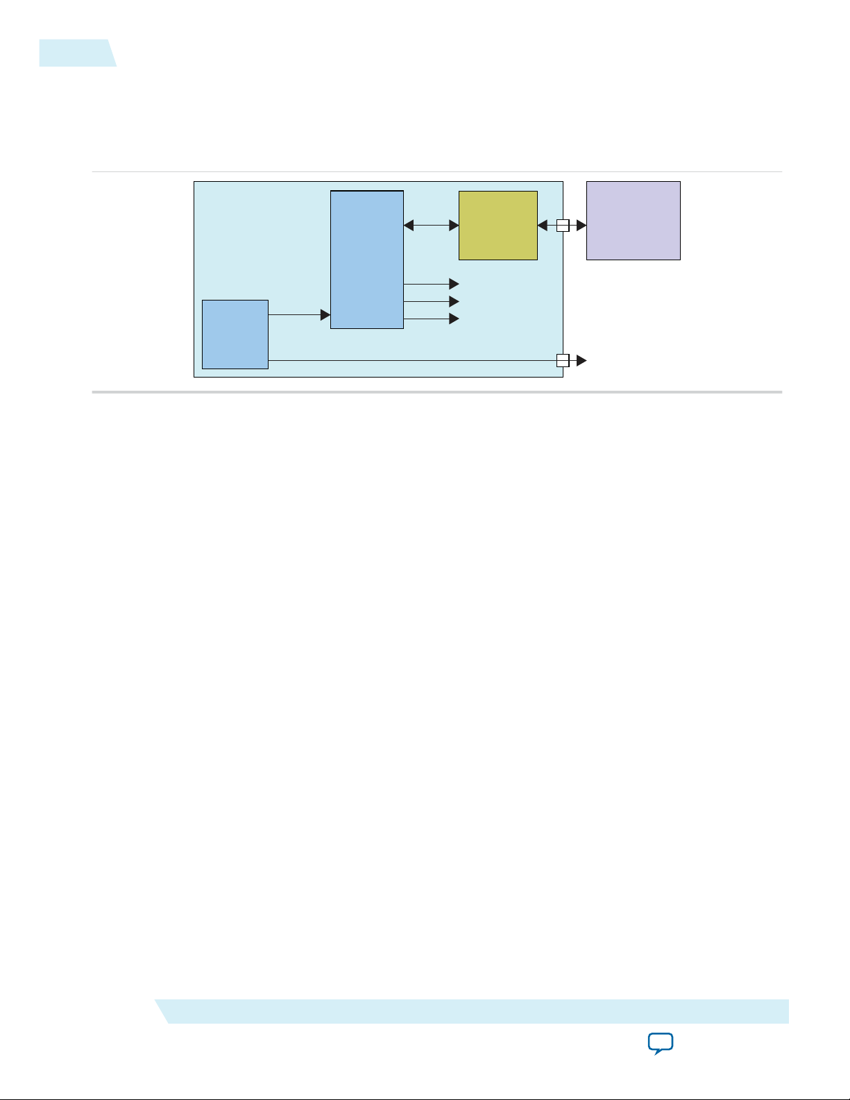
On-Chip Lookup Sensitivity Processing
Altera Advanced SEU Detection IP core interprets the error detection register of the error detection block,
and then compares single-bit error locations with a sensitivity map. This check determines whether or not
the failure affects the device operation.
Figure 1: System Overview for On-Chip Lookup Sensitivity Processing
The Altera Advanced SEU Detection IP core accepts the content of the error message register (EMR) and
issues a query to an external memory containing the sensitivity map. The system designer is responsible
for the memory access logic and external memory.
ALTADVSEU
2015.05.04
Altera recommends that you implement an SEU detection circuit that tolerates a soft error in its logic by
instantiating two instances of the Altera Advanced SEU Detection IP core in your design. In this case, one
instance of the IP core flags errors that occur in the other instance of the IP core as “critical.”
Related Information
• Configuration, Design Security, and Remote System Upgrades in Stratix IV Devices
Provides more information about the design security for Stratix IV devices.
• Configuration, Design Security, and Remote System Upgrades in Arria V Devices
Provides more information about the design security for Arria V devices.
• Configuration, Design Security, and Remote System Upgrades in Cyclone V Devices
Provides more information about the design security for Cyclone V devices.
• Configuration, Design Security, and Remote System Upgrades in Stratix V Devices
Provides more information about the design security for Stratix V devices.
Altera Corporation
Altera Advanced SEU Detection IP Core User Guide
Send Feedback
Page 3
clk
reset
cache_comparison_off
data
valid
error
address
read
byteenable
waitrequest
critical_error
clk
reset
cache_comparison_off
emr[66:0]
emr_valid
emr_error
mem_addr[31:0]
mem_rd
mem_bytesel[3:0]
mem_wait
critical_error
my_asd
Altera Advanced SEU Detection IP Core
noncritical_error noncritical_error
regions_report regions_report
readdata
readdatavalid
mem_data[31:0]
mem_datavalid
ALTADVSEU
2015.05.04
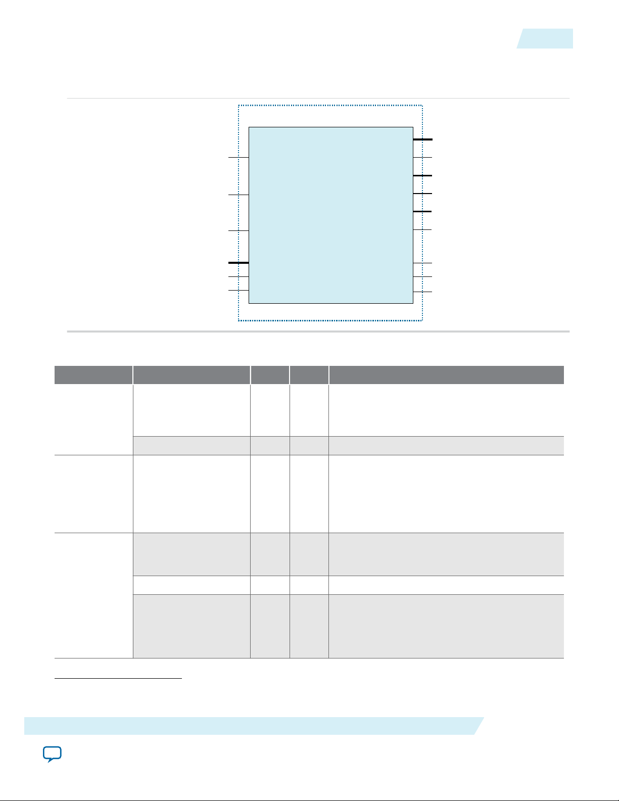
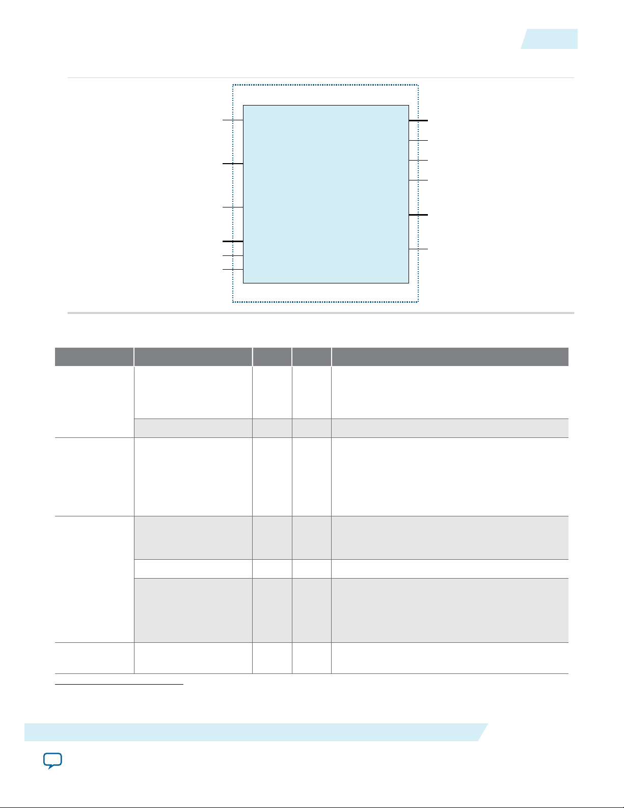
On-Chip Processing Signals
Figure 2: Altera Advanced SEU Detection Core Signals for On-Chip Processing
On-Chip Processing Signals
3
Table 2: Altera Advanced SEU Detection Core Signals for On-Chip Processing
Interface Signals Type Width Description
clk Input 1
• Clock input.
• Recommended frequency is 100 MHz or
Clock and reset
Cache Configu‐
ration
reset Input 1 Active-high reset.
cache_comparison_off Input 1
higher.
• Static input signal.
• Commands the IP core to bypass cache
comparison.
• You can use this signal with the internal
scrubbing feature for custom design.
emr Input 67 Error Message Register data input from the
Altera Error Message Register Unloader IP
core.
Avalon-ST
(Streaming)
Sink Interface
Signals
(1)
emr_valid Input 1 Indicates when emr data input is valid.
emr_error Input 1
• Indicates when emr data will be ignored due
to an error.
• This may occur when there is a data overrun
from the Altera EMR Unloader IP core.
(1)
The Avalon (ST) Streaming Sink Interface should be connected to the corresponding Avalon-ST Source
Altera Advanced SEU Detection IP Core User Guide
Interface of the EMR Uploader IP Core.
Send Feedback
Altera Corporation
Page 4

4
On-Chip Processing Signals
Interface Signals Type Width Description
ALTADVSEU
2015.05.04
Errors Output
External
Memory
Avalon-MM
Master
noncritical_error Outpu
t
critical_error Outpu
t
regions_report Outpu
t
mem_addr
Outpu
t
mem_rd Outpu
t
mem_bytesel Outpu
t
mem_wait Input
1 Indicates that an SMH lookup determined that
the EDCRC error is in a non-critical region.
1 Indicates that an SMH lookup determined that
the EDCRC error is in a critical region.
1
• The ASD region for the error, as reported by
the SMH lookup.
• The width of this port comes from the
setting for the parameter “Largest ASD
region ID used.”
• Output to the user logic.
• Byte address of the 32-bit word to be read.
• Output to the user logic.
• Signals to the user logic to request a read
operation.
• Output to the user logic.
• A four-bit signal that selects the bytes
needed by the IP core. Use of this signal
allows 16-bit or 8-bit memories to optimize
the number of reads in cases where the IP
does not need all 32 bits. If bit 0 of mem_
bytesel is 0, then the IP core ignores bits 0 to
7 of mem_data, and similarly for bits 1 to 3
of mem_bytesel.
• Input from the user logic.
• Signals to the memory interface that the
read operation is still running. Must be high
by the first rising clock after mem_rd is
asserted to hold the IP core in a wait state.
Related Information
Altera Error Message Register Unloader IP Core User Guide
Altera Corporation
mem_data Input
mem_datavalid Input
• Input from the user logic.
• 32-bit data bus. Data must be present if
mem_wait goes high and if mem_rd returns
low.
• Input from the user logic.
• Signals that the mem_data signal contains
valid data in response to a previous mem_rd
request.
Altera Advanced SEU Detection IP Core User Guide
Send Feedback
Page 5
EMR
Unloader
IP Core
Advanced
SEU Detection
IP Core
Error Message
Cache Interface
Error Message
Register Interface
CRAM CRC Error Detected
FPGA
Sensitivity Processor
(e.g., System CPU)
CRC_ERROR
Sensitivity Lookup
Information (SMH)
Stored in System Memory
ALTADVSEU
2015.05.04
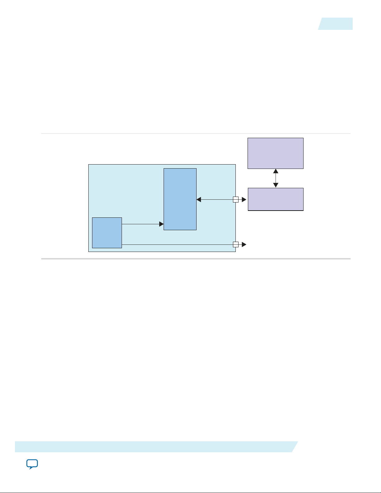
Off-Chip Lookup Sensitivity Processing
The Altera Advanced SEU Detection IP core interprets the content of the error detection block’s EMR
and presents information to a system processor, which determines whether the failure affects the device
operation. The system processor implements the algorithm to perform a lookup against the .smh.
The off-chip lookup sensitivity processing consists of two components:
• Design logic to interpret content of the EMR of the CRC block and present the information to a
processor interface.
• Cache to store off-loaded content of the EMR.
Figure 3: System Overview for Off-Chip Lookup Sensitivity Processing
Off-Chip Lookup Sensitivity Processing
5
The EMR processing unit interprets the content of EMR offloaded from the CRC block by the EMR
Uploader IP core upon an SEU. The EMR processing unit writes each unique EMR value into cache, until
the cache is full. After the cache is full, it asserts a cache overflow flag to the system interface.
For each new value written into cache, the EMR processing unit asserts an interrupt to the processor. The
system processor reads the EMR value and performs a lookup against the .smh to determine the criticality
of a CRAM location. After the system processor services the interrupt, the EMR processing unit advances
the cache line and generates additional interrupt assertions, provided that there is an EMR value in cache
that has not been processed.
After SMH lookup, the system processor determines the required corrective response.
Related Information
• Configuration, Design Security, and Remote System Upgrades in Stratix IV Devices
Provides more information about the design security for Stratix IV devices.
• Configuration, Design Security, and Remote System Upgrades in Arria V Devices
Provides more information about the design security for Arria V devices.
• Configuration, Design Security, and Remote System Upgrades in Cyclone V Devices
Provides more information about the design security for Cyclone V devices.
• Configuration, Design Security, and Remote System Upgrades in Stratix V Devices
Provides more information about the design security for Stratix V devices.
Altera Advanced SEU Detection IP Core User Guide
Send Feedback
Altera Corporation
Page 6
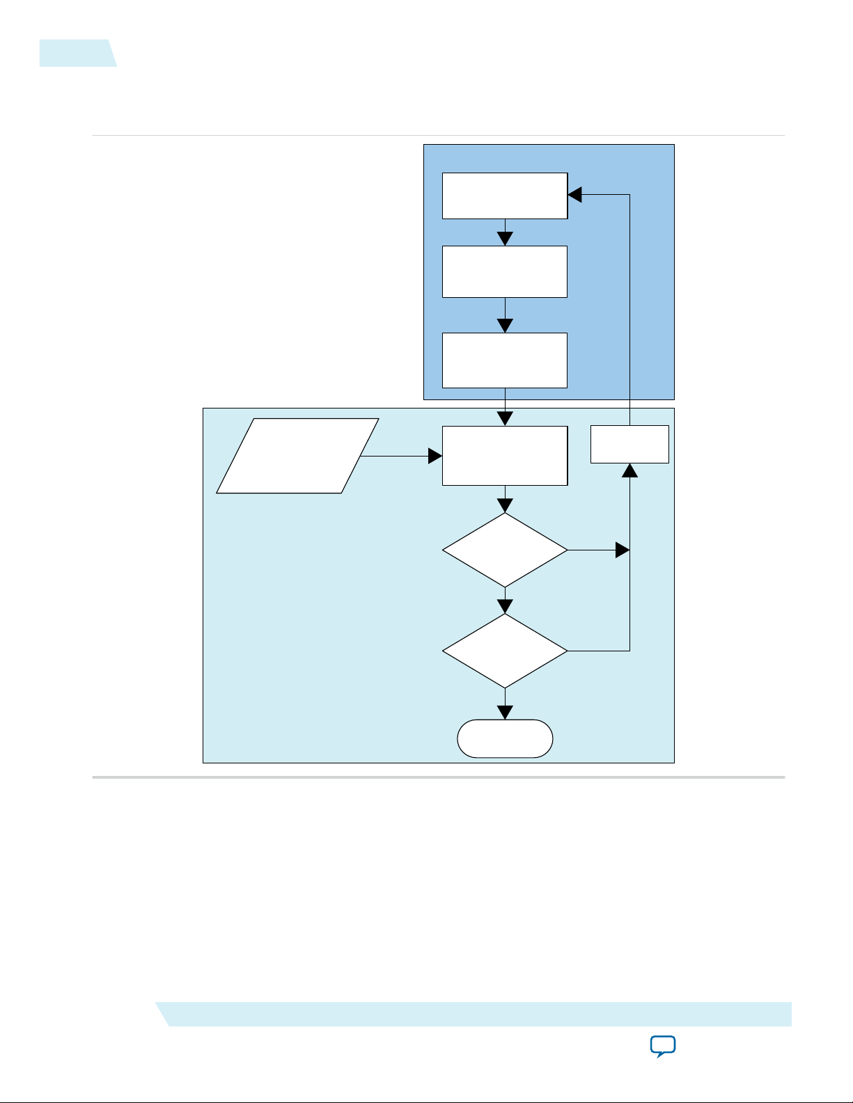
CRC Error Writes a
Value into EMR
CPU Reads SMHSMH File
Bit Critical?
Log Event
Wait for SEU
Corrective
Action Needed?
Reset System
yes
no
yes
no
EMR Processing Unit
System-Level Response
Logic Caches EMR;
Asserts Interupt to CPU
6
Off-Chip Lookup Sensitivity Processing Operation Flow
Off-Chip Lookup Sensitivity Processing Operation Flow
Figure 4: Off-Chip Lookup Sensitivity Processing Operation Flow
ALTADVSEU
2015.05.04
Related Information
SMH Lookup on page 8
Off-Chip Processing Signals
Off-chip sensitivity processing has similar signals with on-chip sensitivity processing, with the exception
of the external memory interface; the off-chip sensitivity processing has EMR cache interface instead.
Altera Corporation
Altera Advanced SEU Detection IP Core User Guide
Send Feedback
Page 7
clk
reset
cache_comparison_off
data
valid
error
data
valid
ready
error
cache_fill_level
critical_error
clk
reset
cache_comparison_off
emr[66:0]
emr_valid
emr_error
cache_data[34:0]
cache_valid
cache_ready
cache_error
cache_fill_level[3:0]
critical_error
my_asd
Altera Advanced SEU Detection IP Core
ALTADVSEU
2015.05.04
Off-Chip Processing Signals
Figure 5: Altera Advanced SEU Detection Core Signals for Off-Chip Processing
7
Table 3: Altera Advanced SEU Detection Core Signals for Off-Chip Processing
Clock and reset
Cache Configu‐
Avalon-ST
(Streaming)
Sink Interface
Signals
Errors Output critical_error Outpu
(2)
Altera Advanced SEU Detection IP Core User Guide
Send Feedback
Interface Signals Type Width Description
clk Input 1
• Clock input.
• Recommended frequency is 100 MHz or
higher.
reset Input 1 Active-high reset.
cache_comparison_off Input 1
ration
• Static input signal.
• Commands the IP core to bypass cache
comparison.
• You can use this signal with the internal
scrubbing feature for custom design.
emr Input 67 Error Message Register data input from the
Altera Error Message Register Unloader IP
core.
emr_valid Input 1 Indicates when emr data input is valid.
(2)
emr_error Input 1
t
• Indicates when emr data will be ignored due
to an error.
• This may occur when there is a data overrun
from the Altera EMR Unloader IP core.
1 Indicates that an SMH lookup determined that
the EDCRC error is in a critical region.
The Avalon (ST) Streaming Sink Interface should be connected to the corresponding Avalon-ST Source
Interface of the EMR Uploader IP Core.
Altera Corporation
Page 8

8
SMH Lookup
Interface Signals Type Width Description
ALTADVSEU
2015.05.04
cache_data Outpu
External
cache_valid Outpu
Memory
Avalon-MM
Master
cache_ready Input 1 Indicates that the reader of the Avalon Stream
cache_error Outpu
Cache Status cache_fill_level Outpu
Related Information
Altera Error Message Register Unloader IP Core User Guide
SMH Lookup
The .smh file represents a hash of the CRAM bit settings on a design. Related groups of CRAM are
mapped to a signal bit in the sensitivity array. During an SEU event, a design can perform a lookup
against the .smh to determine if a bit is used. By using the information about the location of a bit, you can
reduce the effective soft error rate in a running system.
34
t
• Error cache data.
• This is the location information for an EMR
cache entry.
1 Indicates when the cache_data contents are
t
valid.
interface is ready.
1 This Avalon stream control signal indicates the
t
current transfer is in error and should be
ignored.
4 Indicates how many entries are in the cache.
t
The following criteria determine the criticality of a CRAM location in your design:
• Routing—All bits that control a utilized routing line.
• Adaptive logic modules (ALMs)—If you configure an ALM, then the megafunction considers all
CRAM bits related to that ALM sensitive.
• Logic array block (LAB) control lines—If you use an ALM in a LAB, then the megafunction considers
all bits related to the control signals feeding that LAB sensitive.
• M20K memory blocks and digital signal processing (DSP) blocks—If you use a block, then the
megafunction considers all CRAM bits related to that block sensitive.
Related Information
Off-Chip Lookup Sensitivity Processing Operation Flow on page 6
Types of SMH Files
The .smh is an Intel-format Hexadecimal file. You can generate two revisions of .smh files:
• Revision 1—Generated for Stratix IV family devices. This revision does not support hierarchy tagging,
and does not contain tag size or region map information.
• Revision 2—Generated for Arria V, Cyclone V, and Stratix V, and later device families. The
generated .smh contains tag size and region map information.
Altera Corporation
Altera Advanced SEU Detection IP Core User Guide
Send Feedback
Page 9

Sensitivity Data Array
Offset Maps
Frame Information Array
single_offset_map_length
sensitivity_data_array Base Address
offset_map Base Address
frame_info Base Address
32-bit ID: 0x00445341
0x00000014
0x00000000
Header Information
ALTADVSEU
2015.05.04
Revision 1 SMH
Figure 6: Revision 1 SMH
Revision 1 SMH
9
Altera Advanced SEU Detection IP Core User Guide
In revision 1 files, the sensitivity map header starts from 160-bit header information that provides basic
information about the .smh format. This includes the base addresses for the frame information, offset
maps and length of the single offset map, and the sensitivity data array.
• Frame information array—contains a 32-bit string for each frame in the device. The frame number
serves as the index for the frame information string. Each frame information string provides the
following information:
• offset_map_array_index (Bits 7:0)—the index for the offset map array that this frame uses.
• frame_info_data_offset (Bits 31:8)—a 24-bit address offset into the sensitivity array for this
frame.
• Offset map array—The offset map information array is a set of arrays containing 16-bit offset maps.
Each offset map value represents an additional offset into the sensitivity array for a frame group. Each
offset map value is 16 bits. The offset_map_length string in the header information defines the size
of each offset map array.
• Sensitivity data array—The sensitivity data array is a flat-bit vector where 1 specifies a sensitive bit and
0 specifies an insensitive bit.
Altera Corporation
Send Feedback
Page 10

32 bit ID: 0xXX445341
frame_info Base Address
offset_map Base Address
sensitivity_data_array Base Address
single_offset_map_length
sensitivity_data_tag_size
region_map Base Adress
SOF 32 bit CRC Signature
Reserved
Frame Info
Offset Maps
Sensitivity Data Array
Region Map
Header
Information
0x00000000
10
Revision 2 SMH
Revision 2 SMH
Figure 7: Revision 2 SMH
ALTADVSEU
2015.05.04
Altera Corporation
In revision 2 files, the sensitivity map header is an extension of revision 1 header format. The header
information provides basic information about the .smh revision 2, and includes all the revision 1 header
information fields. The additional fields include size of the sensitivity data tag size in bits, base addresses
for the region map, and 32-bit CRC signature of the corresponding .sof file.
The 32-bits ID of the sensitivity map header revision 2 is defined as follows:
• Bits 23:0—Altera sensitivity map header ID 0x445341
• Bits 24:31—a bit mask for the header information with bit 24 reserved
• Bit 25—indicates the presence of sensitivity tag information in the .smh
• Bits 27:26—reserved
• Bit 28—indicates the presence of 32-bit CRC signature of corresponding .sof
• Bits 29:31—reserved
Altera Advanced SEU Detection IP Core User Guide
Send Feedback
Page 11

ALTADVSEU
2015.05.04
Getting Started with Altera Altera Advanced SEU Detection IP Core
• Frame information array—contains a 32-bit string for each frame in the device. The frame number
serves as the index for the frame information string. Each frame information string provides the
following information:
• offset_map_array_index (Bits 7:0)—the index for the offset map array that this frame uses.
• frame_info_data_offset (Bits 31:8)—a 24-bit address offset into the sensitivity array for this
frame.
• Offset map array—The offset map information array is a set of arrays containing 16 bit offset maps.
Each offset map value represents an additional offset into the sensitivity array for a frame group. Each
offset map value is 16 bits. The size of each offset map array is defined by the offset_map_length
string contained in the header information.
• Sensitivity data array—The size of the single sensitivity data entry or tag
(sensitivity_data_tag_size) is in bits and aligned to power of 2. The sensitivity data array is a flat
sensitivity tag vector where a sensitive tag of 0 specifies a bit insensitive for all regions, and non-zero
tag specifies an offset into region map.
• Region map information array—The region map information array contains a 16-bit string for each
non-zero sensitivity tag. The sensitivity data tag serves as the index-1 for the region map array. The
string is a bitmask of the regions, the bit is sensitive for. Each region can be identified in the bitmask by
mask 1 << (Region ID - 1).
Table 4: Revision 2 SMH File Size and ASD Regions Based on Sensitivity Tag
11
These SMH sizes are for Stratix V 5SGXEA7 device with a SOF size of 31,731,193 bytes.
Number of ASD Regions Sensitivity Tag Size (bits) SMH Size (bytes)
1 1 2,296,736
2-3 2 3,984,920
3-15 4 7,361,308
10-127 8 14,114,024
Getting Started with Altera Altera Advanced SEU Detection IP Core
The Altera Advanced SEU Detection IP core must be used along with the Altera EMR Unloader IP core.
The Altera EMR Unloader IP core provides Error Message Register (EMR) contents whenever it detects
an EDCRC error. Connect the EMR, EMR_valid and EMR_error signals from your Altera EMR Unloader
IP variation to the corresponding inputs of your Altera Advanced SEU Detection IP variation.
Installing and Licensing IP Cores
The Altera IP Library provides many useful IP core functions for your production use without purchasing
an additional license. Some Altera MegaCore® IP functions require that you purchase a separate license
for production use. However, the OpenCore® feature allows evaluation of any Altera® IP core in
simulation and compilation in the Quartus II software. After you are satisfied with functionality and
perfformance, visit the Self Service Licensing Center to obtain a license number for any Altera product.
Altera Advanced SEU Detection IP Core User Guide
Send Feedback
Altera Corporation
Page 12

acds
quartus - Contains the Quartus II software
ip - Contains the Altera IP Library and third-party IP cores
altera - Contains the Altera IP Library source code
<IP core name> - Contains the IP core source files
12
Customizing and Generating IP Cores
Figure 8: IP Core Installation Path
Note: The default IP installation directory on Windows is <drive>:\altera\<version number>; on Linux it is
<home directory>/altera/ <version number>.
Related Information
• Altera Licensing Site
• Altera Software Installation and Licensing Manual
Customizing and Generating IP Cores
You can customize IP cores to support a wide variety of applications. The Quartus II IP Catalog and
parameter editor allow you to quickly select and configure IP core ports, features, and output files.
ALTADVSEU
2015.05.04
IP Catalog and Parameter Editor
The Quartus II IP Catalog (Tools > IP Catalog) and parameter editor help you easily customize and
integrate IP cores into your project. You can use the IP Catalog and parameter editor to select, customize,
and generate files representing your custom IP variation.
Note:
The IP Catalog lists installed IP cores available for your design. Double-click any IP core to launch the
parameter editor and generate files representing your IP variation. The parameter editor prompts you to
specify an IP variation name, optional ports, and output file generation options. The parameter editor
generates a top-level Qsys system file (.qsys) or Quartus II IP file (.qip) representing the IP core in your
project. You can also parameterize an IP variation without an open project.
Use the following features to help you quickly locate and select an IP core:
• Filter IP Catalog to Show IP for active device family or Show IP for all device families. If you have no
• Type in the Search field to locate any full or partial IP core name in IP Catalog.
• Right-click an IP core name in IP Catalog to display details about supported devices, open the IP core's
• Click Search for Partner IP, to access partner IP information on the Altera website.
The IP Catalog (Tools > IP Catalog) and parameter editor replace the MegaWizard™ Plug-In
Manager for IP selection and parameterization, beginning in Quartus II software version 14.0. Use
the IP Catalog and parameter editor to locate and paramaterize Altera IP cores.
project open, select the Device Family in IP Catalog.
installation folder, and view links to documentation.
Altera Corporation
Altera Advanced SEU Detection IP Core User Guide
Send Feedback
Page 13

Search for installed IP cores
Double-click to customize, right-click for
detailed information
Show IP only for target device
ALTADVSEU
2015.05.04
Figure 9: Quartus II IP Catalog
Using the Parameter Editor
13
Note: The IP Catalog is also available in Qsys (View > IP Catalog). The Qsys IP Catalog includes
exclusive system interconnect, video and image processing, and other system-level IP that are not
available in the Quartus II IP Catalog. For more information about using the Qsys IP Catalog, refer
to Creating a System with Qsys in the Quartus II Handbook.
Using the Parameter Editor
The parameter editor helps you to configure IP core ports, parameters, and output file generation options.
• Use preset settings in the parameter editor (where provided) to instantly apply preset parameter values
for specific applications.
• View port and parameter descriptions, and links to documentation.
• Generate testbench systems or example designs (where provided).
Altera Advanced SEU Detection IP Core User Guide
Send Feedback
Altera Corporation
Page 14

View IP port
and parameter
details
Apply preset parameters for
specific applications
Specify your IP variation
name and target device
Legacy parameter
editors
14
Specifying IP Core Parameters and Options
Figure 10: IP Parameter Editors
ALTADVSEU
2015.05.04
Specifying IP Core Parameters and Options
Follow these steps to specify IP core parameters and options.
1. In the Qsys IP Catalog (Tools > IP Catalog), locate and double-click the name of the IP core to
customize. The parameter editor appears.
2. Specify a top-level name for your custom IP variation. This name identifies the IP core variation files
in your project. If prompted, also specify the target Altera device family and output file HDL
preference. Click OK.
3. Specify parameters and options for your IP variation:
• Optionally select preset parameter values. Presets specify all initial parameter values for specific
applications (where provided).
• Specify parameters defining the IP core functionality, port configurations, and device-specific
features.
• Specify options for generation of a timing netlist, simulation model, testbench, or example design
(where applicable).
• Specify options for processing the IP core files in other EDA tools.
4. Click Finish to generate synthesis and other optional files matching your IP variation specifications.
The parameter editor generates the top-level .qsys IP variation file and HDL files for synthesis and
simulation. Some IP cores also simultaneously generate a testbench or example design for hardware
testing.
5. To generate a simulation testbench, click Generate > Generate Testbench System. Generate
Testbench System is not available for some IP cores that do not provide a simulation testbench.
6. To generate a top-level HDL example for hardware verification, click Generate > HDL Example.
Generate > HDL Example is not available for some IP cores.
Altera Corporation
The top-level IP variation is added to the current Quartus II project. Click Project > Add/Remove Files
in Project to manually add a .qsys file to a project. Make appropriate pin assignments to connect ports.
Altera Advanced SEU Detection IP Core User Guide
Send Feedback
Page 15

<your_testbench>_tb.csv
<your_testbench>_tb.spd
<your_ip>.cmp - VHDL component declaration file
<your_ip>.ppf - XML I/O pin information file
<your_ip>.qip - Lists IP synthesis files
<your_ip>.sip - Contains assingments for IP simulation files
<your_ip>.v or .vhd
Top-level IP synthesis file
<your_ip>.v or .vhd
Top-level simulation file
<simulator_setup_scripts>
<your_ip>.qsys - System or IP integration file
<your_ip>_bb.v - Verilog HDL black box EDA synthesis file
<your_ip>_inst.v or .vhd - Sample instantiation template
<your_ip>_generation.rpt - IP generation report
<your_ip>.debuginfo - Contains post-generation information
<your_ip>.html - Connection and memory map data
<your_ip>.bsf - Block symbol schematic
<your_ip>.spd - Combines simulation scripts for multiple cores
<your_ip>_tb.qsys
Testbench system file
<your_ip>.sopcinfo - Software tool-chain integration file
<project directory>
<EDA tool setup
scripts>
<your_ip>
IP variation files
<testbench>_tb
testbench system
sim
Simulation files
synth
IP synthesis files
sim
simulation files
<EDA tool name>
Simulator scripts
<testbench>_tb
<ip subcores> n
Subcore libraries
sim
Subcore
Simulation files
synth
Subcore
synthesis files
<HDL files>
<HDL files>
<your_ip> n
IP variation files
testbench files
ALTADVSEU
2015.05.04
Files Generated for Altera IP Cores
Files Generated for Altera IP Cores
The Quartus II software generates the following IP core output file structure:
Figure 11: IP Core Generated Files
15
Table 5: IP Core Generated Files
<my_ip>.qsys
Altera Advanced SEU Detection IP Core User Guide
Send Feedback
File Name Description
The Qsys system or top-level IP variation file. <my_ip> is the name
that you give your IP variation.
Altera Corporation
Page 16

16
Files Generated for Altera IP Cores
File Name Description
<system>.sopcinfo Describes the connections and IP component parameterizations in
your Qsys system. You can parse its contents to get requirements
when you develop software drivers for IP components.
Downstream tools such as the Nios II tool chain use this file.
The .sopcinfo file and the system.h file generated for the Nios II tool
chain include address map information for each slave relative to each
master that accesses the slave. Different masters may have a different
address map to access a particular slave component.
<my_ip>.cmp The VHDL Component Declaration (.cmp) file is a text file that
contains local generic and port definitions that you can use in VHDL
design files.
ALTADVSEU
2015.05.04
<my_ip>.html
A report that contains connection information, a memory map
showing the address of each slave with respect to each master to
which it is connected, and parameter assignments.
<my_ip>_generation.rpt IP or Qsys generation log file. A summary of the messages during IP
generation.
<my_ip>.debuginfo Contains post-generation information. Used to pass System Console
and Bus Analyzer Toolkit information about the Qsys interconnect.
The Bus Analysis Toolkit uses this file to identify debug components
in the Qsys interconnect.
<my_ip>.qip
Contains all the required information about the IP component to
integrate and compile the IP component in the Quartus II software.
<my_ip>.csv Contains information about the upgrade status of the IP component.
<my_ip>.bsf A Block Symbol File (.bsf) representation of the IP variation for use
in Quartus II Block Diagram Files (.bdf).
<my_ip>.spd
Required input file for ip-make-simscript to generate simulation
scripts for supported simulators. The .spd file contains a list of files
generated for simulation, along with information about memories
that you can initialize.
<my_ip>.ppf The Pin Planner File (.ppf) stores the port and node assignments for
<my_ip>_bb.v You can use the Verilog black-box (_bb.v) file as an empty module
<my_ip>.sip Contains information required for NativeLink simulation of IP
<my_ip>_inst.v or _inst.vhd HDL example instantiation template. You can copy and paste the
Altera Corporation
IP components created for use with the Pin Planner.
declaration for use as a black box.
components. You must add the .sip file to your Quartus project.
contents of this file into your HDL file to instantiate the IP variation.
Altera Advanced SEU Detection IP Core User Guide
Send Feedback
Page 17

ALTADVSEU
2015.05.04
Files Generated for Altera IP Cores
File Name Description
<my_ip>.regmap If the IP contains register information, the .regmap file generates.
The .regmap file describes the register map information of master
and slave interfaces. This file complements the .sopcinfo file by
providing more detailed register information about the system. This
enables register display views and user customizable statistics in
System Console.
17
<my_ip>.svd
<my_ip>.v
or
<my_ip>.vhd
mentor/
aldec/
/synopsys/vcs
/synopsys/vcsmx
Allows HPS System Debug tools to view the register maps of
peripherals connected to HPS within a Qsys system.
During synthesis, the .svd files for slave interfaces visible to System
Console masters are stored in the .sof file in the debug section.
System Console reads this section, which Qsys can query for register
map information. For system slaves, Qsys can access the registers by
name.
HDL files that instantiate each submodule or child IP core for
synthesis or simulation.
Contains a ModelSim® script msim_setup.tcl to set up and run a
simulation.
Contains a Riviera-PRO script rivierapro_setup.tcl to setup and run a
simulation.
Contains a shell script vcs_setup.sh to set up and run a VCS
®
simulation.
Contains a shell script vcsmx_setup.sh and synopsys_ sim.setup file to
set up and run a VCS MX® simulation.
/cadence
/submodules Contains HDL files for the IP core submodule.
<child IP cores>/ For each generated child IP core directory, Qsys generates /synth and /
Altera Advanced SEU Detection IP Core User Guide
Send Feedback
Contains a shell script ncsim_setup.sh and other setup files to set up
and run an NCSIM simulation.
sim sub-directories.
Altera Corporation
Page 18

18
Altera Advanced SEU Detection IP Core Parameters
Altera Advanced SEU Detection IP Core Parameters
ALTADVSEU
2015.05.04
Parameter
Group
General
Sensitivity
Data
Access
Parameter
Name Legal Value
CRC error cache depth 2, 4, 8,16, 32,
64
Largest ASD region ID 1 to 16
Use on-chip sensitivity
ON, OFF
processing
Memory interface
—
address width
Description
• Specifies how many non-critical cyclic
redundancy check (CRC) error to ignore.
• Default value is 8.
• Indicates the largest ASD SEU detection
region ID in your design.
• Configures the width of the regions_report
port.
• Default value is 1.
• Configures the IP core to use on-chip
sensitivity processing or off-chip sensitivity
processing.
• When enabled, implements an external
memory interface in the IP.
• Specifies width of the address bus connected
to the external memory interface.
• Default value is 32.
Sensitivity data start
address
—
• Specifies the offset added to all addresses the
external memory interface generates.
• Default value is 0x0.
SEU Mitigation on CRAM Array
Critical applications require an SEU recovery strategy. The Quartus II software provides SEU detection,
and allows you to design a recovery response to reduce SEU disruption.
Enabling the Advanced SEU Detection Feature in the Quartus II Software
To enable the Advanced SEU Detection feature in the Quartus II software and generate an .smh, turn on
Generate SEU sensitivity map file (.smh) in the Device and Pin Options dialog box (Assignments >
Device > Device and Pin Options).
Hierarchy Tagging
The Quartus II hierarchy tagging feature enables customized soft error classification by indicating design
logic susceptible to soft errors. Hierarchy tagging improves design-effective FIT rate by tagging only the
critical logic for device operation. You also define the system recovery procedure based on knowledge of
logic impaired by SEU. This technique reduces downtime for the FPGA and the system in which the
FPGA resides. Hierarchy tagging is available only for Arria V, Cyclone V, Stratix V, and later device
families.
Altera Corporation
Altera Advanced SEU Detection IP Core User Guide
Send Feedback
Page 19
ALTADVSEU
2015.05.04
The .smh contains a mask for design sensitive bits in a compressed format. The sensitivity mask is
generated for the entire design. Hierarchy tagging provides the following benefits:
• Hierarchy tagging provides the following benefits:
• Increases system stability by avoiding disruptive recovery procedures for inconsequential errors.
• Allows diverse corrective action for different design logic.
Using Partitions to Specify Logic Sensitivity ID
In the Quartus II software, you can designate a design block as a design partition. You can then assign a
sensitivity value to the partition.
The PARTITION_ASD_REGION_ID global assignment specifies the numeric value from 0 to 16. The value
represents the sensitivity tag associated with this partition:
set_global_assignment -name PARTITION_ASD_REGION_ID <asd_id> -section_id
<partition_name>
A sensitivity tag of 1 is the same as no PARTITION_ASD_REGION_ID assignment, specifying basic sensitivity
level: "region used in design". If a soft error occurs in this partition, the error is reported back as a critical
error in the sensitivity region 1.
A sensitivity tag of 0 is reserved, as indication that CRAM bits are not used in your design. You can
explicitly set it to indicate that partition is not-critical, and force the partition to be completely excluded
from the sensitivity mapping.
Using Partitions to Specify Logic Sensitivity ID
19
Note:
You can create multiple partitions with the same sensitivity tag in a design.
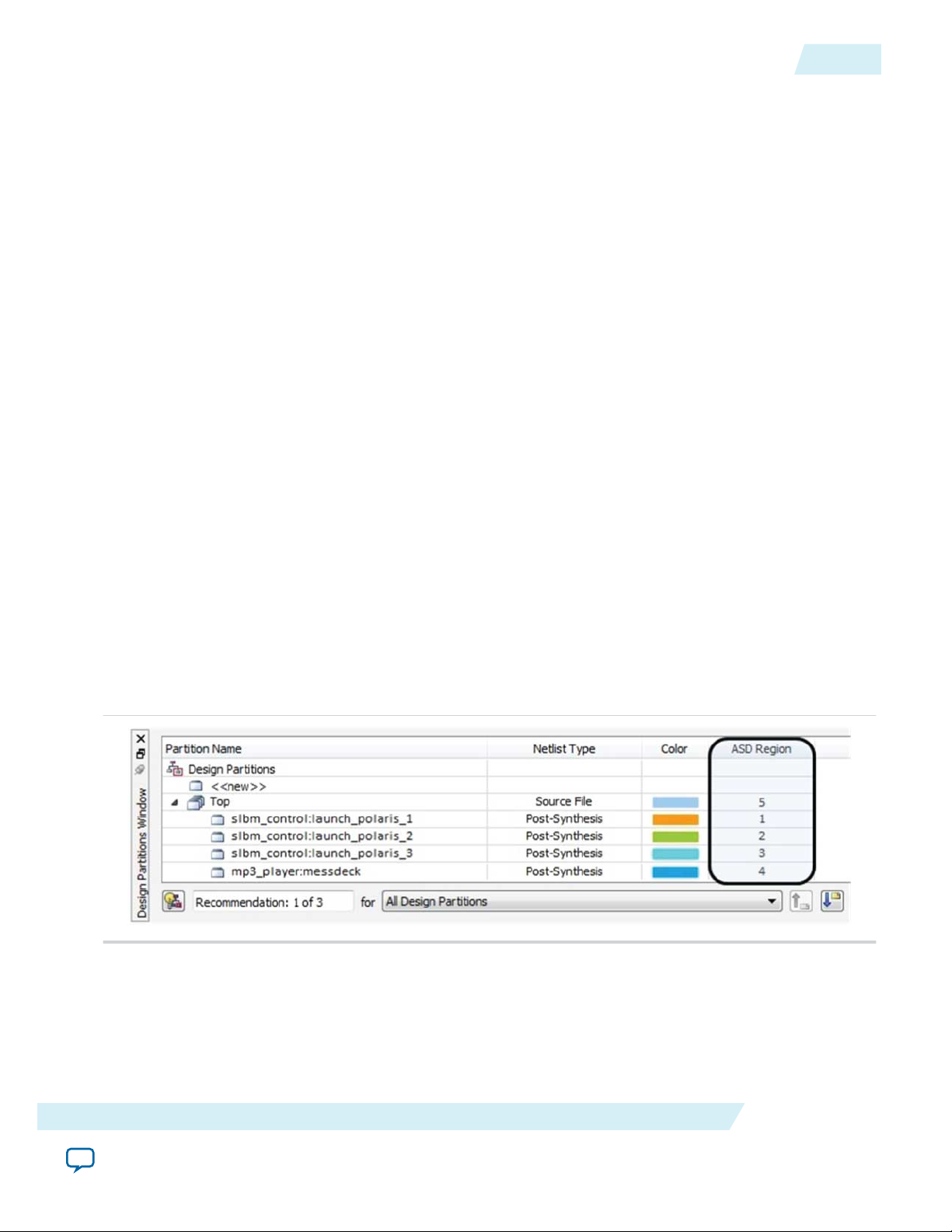
Design Partitions Properties
Specify the sensitivity ID assigned to the partition in the ASD Region column in the Design Partition
window.
Figure 12: ASD Region Column in the Design Partition Window
Sensitivity Map Header File Lookup
The .smh contains critical bit information about the design. The sensitivity data is generated as a standard
Intel hex (big-endian) .smh file during .sof generation.
Altera Advanced SEU Detection IP Core User Guide
Send Feedback
Altera Corporation
Page 20

20
Programming a Sensitivity Map Header File into a Memory
Programming a Sensitivity Map Header File into a Memory
You can program a .smh into any type of memory. For example, to use CFI flash memory, follow these
steps:
1. Rename the .smh to <file_name>.hex, or convert it to little-endian <file_name>.hex if required.
2. In the Quartus II software, click File > Convert Programming Files.
3. In the Convert Programming Files window under Output programming file, select the desired
options.
4. To add hex data, follow these steps:
Figure 13: Add Hex Data Dialog Box
ALTADVSEU
2015.05.04
a. Click Add Hex Data.
b. In the Add Hex Data dialog box, turn on Set start address and enter a start address.
c. In the Hex file box, click browse to select the .hex file, and click OK.
5. Click Generate.
Performing a Lookup for SMH Revision 1
To perform a lookup into the sensitivity map header data using a bit, byte, and frame number from an
EMR (Stratix IV devices only):
1. Read the 32-bit frame information string for the frame number:
• Address = 0x14 + (frame*4)
• Return value = (frame_info_data_offset, offset_map_array_index)
2. Read the offset map information for a frame. The return value for the offset map information is 16 bits:
• Address = offset_map_base_address + offset array for current frame + offset data value for
current byte and bit
where,
Altera Corporation
Altera Advanced SEU Detection IP Core User Guide
Send Feedback
Page 21

ALTADVSEU
2015.05.04
• Offset array for current frame = offset_map_array_index * offset_map_length
• Offset data value for current byte and bit = [(byte * 8) + bit] * 2
• Return value = offset_map_value
3. Read the 8-bit sensitivity value:
• Address = (offset_map_value/8) + sensitivity_base_address + frame_info_data_offset
• Return value = sensitive_bit_word[7:0]
4. Read the sensitive bit. The offset map value provides the sensitive bit index. A value of 1 indicates a
critical bit, and a value of 0 indicates a non-critical bit.
• Sensitive bit = sensitive_bit_word[bit_index]
where,
• bit_index = offset_map_value[2:0]
Performing a Lookup for SMH Revision 2
To perform a lookup into the sensitivity map header data using a bit, byte and frame number from an
EMR (Arria V, Cyclone V, Stratix V, and later devices only):
1. Read the 32-bit frame information string for the frame number:
Performing a Lookup for SMH Revision 2
21
• Address = 0x1C + (frame*4)
• Return value = (frame_info_data_offset, offset_map_array_index
2. Read the offset map information for a frame. The return value for the offset map information is 16 bits:
• Address = offset_map_base_address + offset array for current frame + offset data value for
current byte and bit
where,
• Offset array for current frame = offset_map_array_index * offset_map_length
• Offset data value for current byte and bit = [(byte * 8) + bit] * 2
• Return value = offset_map_value
3. Read the 8-bit sensitivity value:
• Address = (offset_map_value * sensitivity_data_tag_size /8) + sensitivity_base_address
+ frame_info_data_offset
• Return value = sensitive_bit_word[7:0]
4. Read sensitivity data tag. The offset map value provides the sensitive bit index. The return value for the
sensitivity tag is sensitivity_data_tag_size bit length. A zero tag indicates that bit is not critical for
any region while a non-zero tag indicates offset in region map.
• sensitive_tag = (sensitive_data word >> tag_shift) and tag_mask
where,
• tag_shift = (offset_map_value * sensitivity_data_tag_size)[2:0]
• tag_mask = (0x1 << sensitivity_data_tag_size) - 1;
5. Read the region mask for a non-zero sensitivity tag. The return value for the region mask is 16 bits.
• region_mask = region_map_base_address + (sensitivity_data_tag - 1) * 2
Altera Advanced SEU Detection IP Core User Guide
Send Feedback
Altera Corporation
Page 22

22
Document Revision History
Note: The possible values for sensitivity_data_tag_size field are 1,2,4 or 8 that allows to support
a maximal of 255 possible non-zero region masks for a design.
Document Revision History
Table 6: Document Revision History
Date Version Changes
ALTADVSEU
2015.05.04
May 2015 2015.05.04
• Added note to possible values for sensitivity_data_tag_size
field.
• Updated largest ASD region ID in the Altera Advanced SEU
Detection IP Core Parameters.
• Updated supported device for performing Lookup for
Revision 1 and 2.
• Updated features and device family support by combining
in a table.
• Removed duplicated signals in Off-Chip processing signals
table.
• Updated SMH frame information array description to
reduce redundancies.
June 30 2014 2014.06.30
• Updated supported devices.
• Replaced information about the MegaWizard Plug-in
Manager with the IP Catalog.
December 2012 1.0 Initial release.
Altera Corporation
Altera Advanced SEU Detection IP Core User Guide
Send Feedback
 Loading...