

Page 1
SERVICE MANUAL
TO ALPINE Home Page
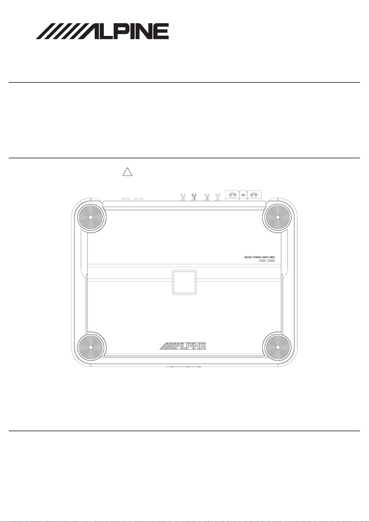
MONO POWER AMPLIFIER
Caution : The part marked with ! is generating a high voltage, so care will be necessary when working.
PDX-1.1000
4 / 06-A
A06008
Page 2
<Cautions for Safe Repair Work>
r
s
- 2 -
The following cautions will prevent accidents in the workplace and will ensure safe products.
*The symbols indicate caution is needed to prevent injuries and damage to property.
The symbols and their meanings follow.
Warning
Caution
*The following symbols indicate two levels of cautions.
When you see this symbol, you have to be very careful.
When you see this symbol, you have to follow the instructions there.
If you ignore this symbol and handle the product incorrectly or unsafely,
serious injury or death may result.
If you ignore this symbol and handle the product incorrectly or unsafely,
injury or only material damage may result.
Warning
Do not look squarely into the laser light
coming from the pickup. Always use a designated fuse.
You may loose you sight. Use of an incorrect fuse may result in a fire.
Caution
Do not allow wiring to be caught in the Battery Caution
screw/chassis. Use the designated battery.
If wiring is caught in the screw/chassis, it may Confirm the correct polarity and seat of the
cause a short circuit, resulting in a fire. battery.
Fuse Caution
An incorrect battery or an improperly connected
or seated battery may result in a fire.
High Temperature Caution Designated Parts Caution
Touching the heat sink may cause severe burns. Look up the part list and ensure that only
designated parts are used to prevent problems or
accidents.
Reverse Power Supply Connections o
Misconnections Caution Ensure that the wiring is correct when rewiring to
Reverse power supply connections or prevent problems with ignition/breakdown.
misconnections may cause ignition problems and
smoke may result.
Soldering Caution Wear Glove
Hot solder from solder splash may cause severe Wear gloves to prevent electrical shocks or injury
burns. from the end face of the metal.
Wiring Caution
Page 3

Contents
- 3 -
PDX-1.1000
Packing Assembly Parts List
Packing Method View
Specifications
Extension Cable
Block Diagram
Parts Layout on P.W.Boards and Wiring Diagram
Schematic Diagram
Terminal Voltage of IC/TR
8 to 10
11 to 13
14 to 18
Description of IC Terminal
Exploded View (Cabinet)
About Semi-fixed VR (VR401) of MAIN P.W.Board
4
4
5
6
7
19
20
21
NOTE : Due to continuing product improvement, specifications and designs are subject to
change without notice.
Page 4
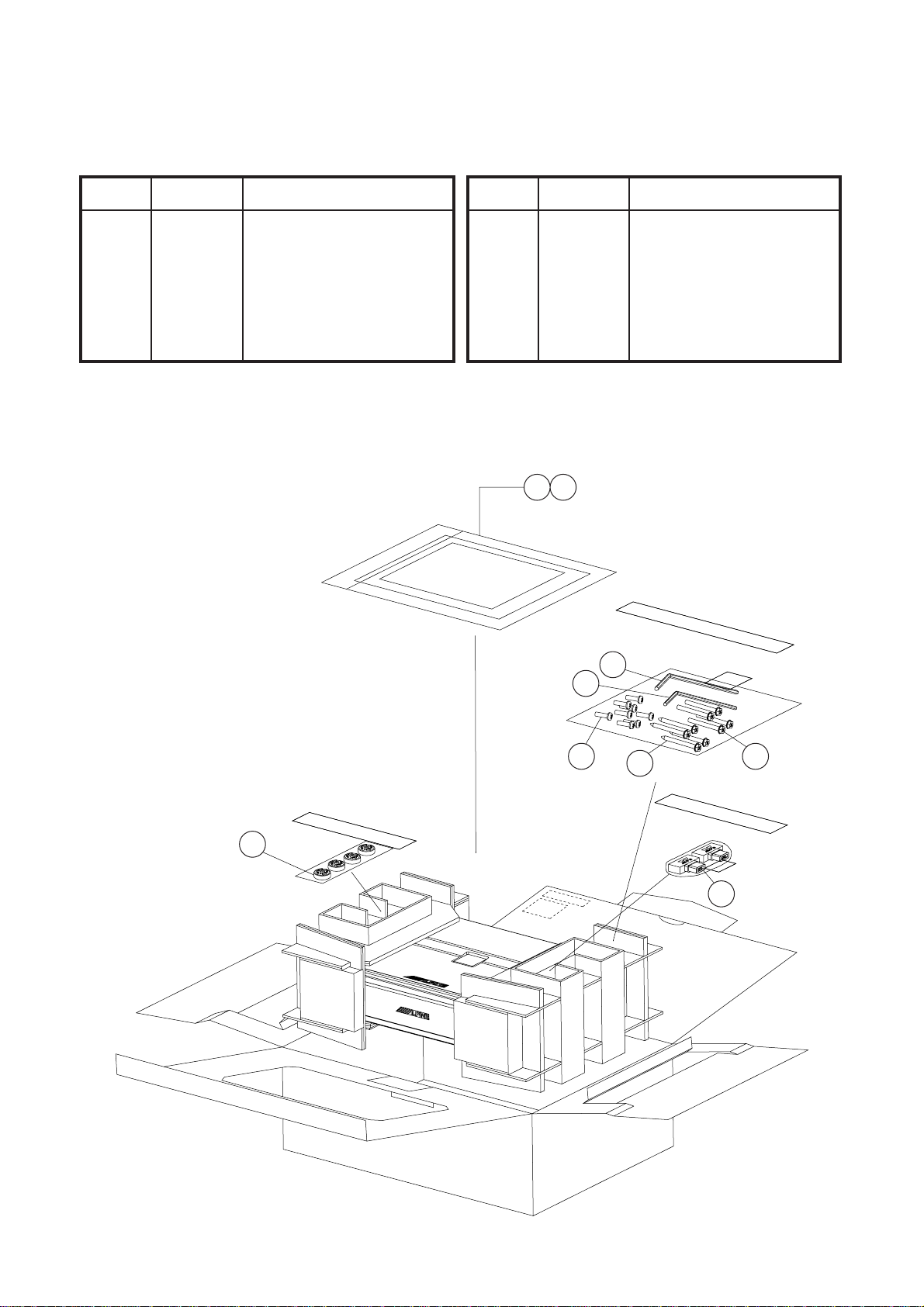
PackingAssembly Parts Lis
t
TO CONTENTS
- 4 -
PDX-1.1000
Symbol Symbol
Part No. Description Part No. Description
No. No.
101
#1
101
$1
101
%1
101
&1
102 68-05946Z03 MANUAL,OWNER'S-IGS 109 03E39508S01 SCR,M4X40(WP)(BLK)
$1
103 09E39816S01 CONN,PLUG 2P
104 42E39219S01 JOINT,TOP
NOTE : #1 : For North American Model Only, $1 : For European Model Only, %1 : For General Foreign Model Only,
&1 : For Chinese Model Only, Others : Common.
68-05946Z01 MANUAL,OWNER'S(AO)
68-05946Z02 MANUAL,OWNER'S-GO
68-05946Z02 MANUAL,OWNER'S-GO
68-05946Z66 O/M AOCH
105 03E36691S01 WRENCH,2X2.3
106 03E36692S01 WRENCH,4X4.6
107 03E39493S01 SCR,M2.6X14(P)(WHT)
108 03E39500S01 SCR,M4X36(WSP)(BLK)
Packing Method View
101
102
104 X4
105
107 X8
106
109 X4
108 X4
103 X2
Page 5
PDX-1.1000
Specifications
TO CONTENTS
- 5 -
Power Output (1) 20Hz, 4ohm, 1.0% T.H.D. (14.4V) 1000W
100Hz, 4ohm, 1.0% T.H.D. (14.4V) 1000W
(2) 20Hz, 2ohm, 1.0% T.H.D. (14.4V) 1000W
100Hz, 2ohm, 1.0% T.H.D. (14.4V) 1000W
T.H.D. (100Hz, 400W/ 4ohm (14.4V)) 1.0%
Residual Noise (Input Short) 20mV
S/N Ratio (Ref.Output 1000W/ 4ohm, Input Short) 80dB
Frequency Response (Ref.Output 1W/ 4ohm, Ref.Frequency 100Hz) 20Hz : -0.5±2dB
200Hz : -3.5±2dB
Output Offset Voltage (No Signal) ±150mV
Remote On Voltage (1W Output) 6.4±1V
Current Drain (1) No Signal 3.0A
(2) 10% T.H.D., 2ohm Load 150A
(3) Remote Current Drain 0.27±0.2mA
(4) Back Up Current Drain 1.2mA
Input Sensitivity (Ref.Output 1000W/ 4ohm, 100Hz) (Input sensitive volume position : MAX)
Input level switch position : 0.1Vrms~1.0Vrms 125mV±3dB
Input level switch position : 1.0Vrms~8.0Vrms 1000mV±3dB
SUB-SONIC Filter (Input 100Hz, Ref.Output 1W/ 4ohm)
SUB-SONIC Filter switch position : 15Hz -4.0dB±2dB
SUB-SONIC Filter switch position : 30Hz -3.4dB±2dB
Pre-Out Level at 1.0V Input 1.0V±3dB
Input Impedance (Reference) 29.2kohm±10%
Fuse Requirement 20A(Peak) x 4 (For Battery Line)
Power Source DC14.4V (11 to 16V)
Dimensions (W x H x D) 257 x 62 x 192mm
Weight 3.41kg
NOTE : Due to Continuing product improvement, specifications and designs are subject to change without notice.
Page 6
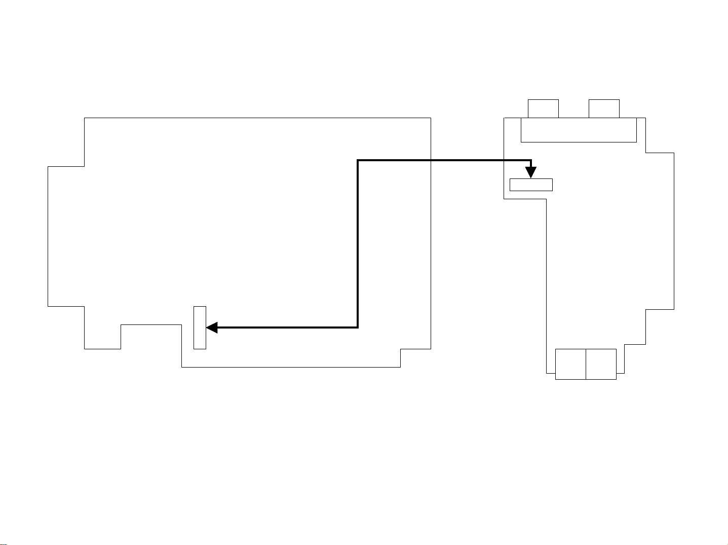
Extension Cable
TO CONTENTS
- 6 -
PDX-1.1000
*Always connect the Extension Cable when making checks of voltage and repair.
(1)
CB201
CB901
MAIN P.W.Board
SUB P.W.Board
(1) 01E35763S01
Page 7
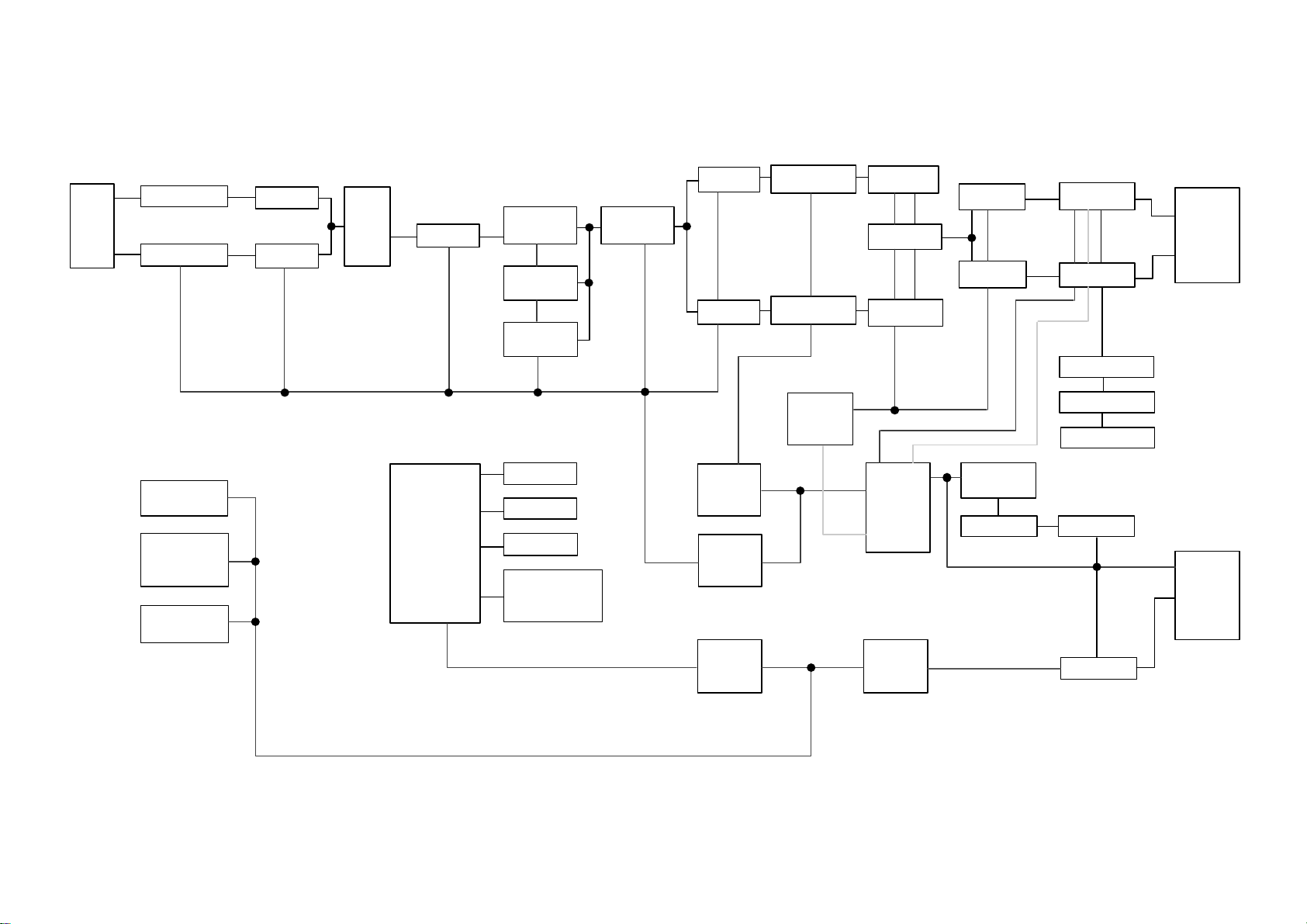
Block Diagram
TO CONTENTS
- 7 -
RCA
JACK
IN L
IN R
INPUT BUFFER
INPUT BUFFER INPUT ISO
TOP LED SUPPLY
BLUE RESET ±5V
FRONT LED u-COM B-DET POWER
BLUE SUPPLY
RED
FRONT LED
BLUE GND
INPUT ISO
INPUT
LEVEL
S/W
IPUT GAIN
LIMITER INTEGRATOR1 INVERTER1
DRIVER1
SUB SONIC
S/W
SUB SONIC DRIVER2
15Hz
SUB SONIC
30Hz
V-DET POWER DC-DC
TRANS THER
INTERNAL THER
LPF
50Hz~200Hz
AND GATE
INVERTER INVERTER2
±15V
POWER POWER
SUPPLY SUPPLY REMOTE+B
+5V +8V
INTEGRATOR2
POWER OVER CURR1
SUPPLY
VSS±12V
±25V
±60V
DC-DC
TRANS
CONTROL
VOLTAGE SW+B
PDX-1.1000
OUTPUT FET
OUTPUT+
OUTPUT-
OUTPUT FET
CURRENT LIMIT
OUTPUT THER
BATTERY
REMOTE
Page 8

Parts Layout on P.W.Boards and Wiring Diagram (1/3)
- 8 -
TO CONTENTS
Caution:The part marked with is generating a high voltage,
MAIN P.W.Board (Component Side View)
R306
C305
C307
R307
R314 R313
R310
R309
C304
R815
C303
D301
R303
R308
R332
R333
R305
R304
E302
R301
C301
C302
D302
R340
C323
D307
D308
R302
E301
R338
Q308
Q307
E B
Q302
R341
E303
E304
C324
B E
B E
E911
C945
R322
R337
R325
R339
C317
R342
Q310
E B
1 5
IC310
3 4
C325
5 4
C322
1 3
Q305
E B
R327
R344
R343
IC309
ZD302
R345
C327
R346
R336
R335
IC909
ZD852
ZD806
ZD805
ZD851
ZD803
B E
ZD801
R878
ZD802
ZD804
D852
R877
Q801
B E
R875
E910
R876
B E
R873
Q856
Z933
T904
C944
Q802
D851
R874
E B
E B
R872
IC908
Q857
Q855
R871
1
2
(CH701)
From LED P.W.Board
BLK
RED
2
1
R702
R701
To CB701
D401
C419
Q701
R401
R409
LUG7
B E
R402
R408
R712
R403
R407
R711
E403
R330
C320
C321
D303
C316
D304
C318
C319
IC308 IC307
IC304
IC305
IC306
C309
C311C310
D306
R808
D305
CB701
C804
Q303
E C
E308
Q304
E C
R819
IC802
R818
C308
C306
R311
IC301
IC302
R312
C803
so care will be necessary when working.
C326
Z931
E311
30
To CB901
2
E310
LUG5
29
1
B E
ZD301
(CB201)
From SUB P.W.Board
Q306
R321
R347
R348
R349
R350
R351
D908 D905
LUG6
CB901
Z932
LUG4
PDX-1.1000
Q703
Q702
B E
B E
C938
C939
3
4
5
Orange Color Pattern:Component Side Pattern
Blue Color Pattern:Foil Side Pattern
Q401
Q402
Q404
Q403
Q408Q407 Q406 Q405
1 3
6 4
C403
R415
R410
R411
R412
R424
C409
R414
D404D403 D402
C410
C420
Q881
R802
R413
R418
R881
LUG11
R417
R803
R445
R416
R446
R801
C801
R449
E401
E402
E404
C447
C442
C457
R448
C451
T4
0
1
T402
C449
C448
C450
R441
R419
R422
R442
C414
R443
R444
R423
R439
VR401
C401
C411
IC405
IC404
E922
E925
C412
E924
E923
C402
C456
CB401
R938
R940
E B
Q931
LUG9
R967
R970
R969 R968
B E
B E
E933
C441
Q935
Q932
E931
R947
R941
E904
R952
D932
C920
E903
C921
T903
D931
ZD931
E908
E909
L901
F902 F901
F004
F003
C942
R950
R943
IC901
SD902
SD904
SD905
SD903
IC902
C936
TH931
LUG3
C934
F002
F001
L902
E902
E901
C932
T902 T901
C933
C931
L931
TML901
LUG2
Q926
LUG1
321
A
BC DE F G
Page 9

Parts Layout on P.W.Boards and Wiring Diagram (2/3)
- 9 -
TO CONTENTS
Caution:The part marked with is generating a high voltage,
so care will be necessary when working.
1
MAIN P.W.Board
(Foil Side View)
G S
D D
Q911 Q910
S G
D D
G S
D D
Q915 Q914
S G
D D
G S
D D
Q919 Q918
S G
D D
Q923Q922
G S
D D
S G
D D
Q902
G S
D D
Q904
G S
D D
Q906
G S
D D
Q908
G S
D D
R918 R917
C913
R919
R920
R954
R905
C914
R921
R922
R915R914
C912
IC903
D902
R916
C906
TP904
C908
IC905
R924 R923
R956
C907
C902
R911
R907
R910
IC904
C915
C901
R909
D901
IC906
C911
R901
R906
C904 C903
R908
C910
R964
Q901
E B
R904
C909
D903
R960
R962
R955
D904
Q934
E B
SD906
TP858
TP859
TP857
R912
R913
C905
SD901
TP862
TP861
TP956
R966 R965
E B
R902
R903
Q936
TP860
TP951
C986
2
4
3
LD705
LD703
D D
D D
D D
D D
G S
Q903
G S
Q905
G S
Q907
G S
Q909
R706
R705
R704
R703
G S
Q912
D D
G S
Q913
D D
G S
Q916
D D
G S
Q917
D D
G S
Q921
D D
G S
Q920
D D
G S
D D
Q925
G S
D D
Q924
TP954
R939
R942
R945
R946
TP952
TP950
TP301
TP302
C405
R437
C404
R438
TP308
TP306
TP305
TP307
TP304
TP310
R421 R420
C413
R440
TP309
TP425
TP423
TP303
TP410
TP411
R319
TP312
TP321
R316
R315
TP322
R317
R318
D408
C314
R320
TP316
C315
R324 R323
TP315
TP311
D407
D410
C312
TP318
TP319
TP317
C313
TP320
R329
TP313
R331
TP314
D409
R328
TP324
TP323
R326
TP326TP325
R406
R405
R404
C445
C446
LD701
TP419
TP415
TP416
TP409
TP405
TP413
TP406
TP412
TP408
TP414
TP407
TP422
TP418
TP421
TP417
PDX-1.1000
5
Orange Color Pattern:Component Side Pattern
Blue Color Pattern:Foil Side Pattern
A
TP949
TP939
TP947
BC DE F G
Page 10

Parts Layout on P.W.Boards and Wiring Diagram (3/3)
- 10 -
TO CONTENTS
PDX-1.1000
1
CH701
ASSY,CON 2P
RED
BLK
2
GND8V
LED P.W.Board
(Component Side View)
3
TP6002
LD4001
TP6001
C4001
4
R4002 R4001
LED P.W.Board
(Foil Side View)
5
Orange Color Pattern:Component Side Pattern
Blue Color Pattern:Foil Side Pattern
From MAIN P.W.Board (CB701)
JK102JK101
R127
3 1
4 2
3 1
4 2
TP209
R226
TP203
R218 R217
R219
R128
R124
R123
C203
R205
TP210
C216
R224
R220
R201
R204
R222
R203 R202
TP139
TP208
R209
R221
Z102Z101
R216
R210
TP201
R106R105 R104 R103R102 R101
R126R125
R208
TP202
R207
R215
TP124
E103
E104
E101
E102
TP143
R213
C213
C215
R214
C212
R212
R211
C214
C219
C221
MT14
C109 C108 C107 C106
TP132
TP204
D103
R107
D104
R108
D101
R109
D102
R110
SUB P.W.Board
(Component Side View)
R114
E109
C121
IC102
E110
C111
R120
TP137
TP140
TP142
C515
Z501
R112
R113
IC101
R111
TP141
TP135
TP133
C120
C118
C119
TP131
TP129
Z502
C516
TP144
E202
E201
E107
E108
MT13
R118 R117
C123 C122
R115
R119
R116
TP125
TP123
C987
C113
IC103
C112
C110
TP128
C983
R122
R121
TP130
R984
C117
C116
C114
TP122
TP120
TP121
R986
C984
R983
3 1
4 5
C982
C115
TP126
TP127
TP119
TP981
R982
ZD981
D981
IC981
TP118
R989
TP983
R987
R985
R981
TP982
R525
Q502
C985
Z901
C981
C507
RA504
RA502
B E
1 5
3 4
R521
R520
R515
RA505
RA503
IC503
C501
R514
R512
TH501
C512
5 4
1 3
R513
E501
R517
R509
C510
IC506
C513
R518
IC505
R516
4 5
IC508
C514
MT11 MT10
R506
FD2
R527
CL501
R502
RA506
C506
4 3
5 1
IC501
R526
R507
IC504
C504
IC502
C503
C517
R508
R505
FD1
RA501
C502
R501
R503
D501
C508
R504
C505
SUB P.W.Board
(Foil Side View)
R524
Q501
B E
3 1
R523
C509
R522
IC507
R519
C511
C225C224
R227R225
C202C201
C232
C223
C218
C217
C220
IC201
TP103
MT8
IC205
SW201
VOL201
SW101
VOL202
TP102
MT9
1
2
CB201
To CB201
(CB901)
29
30
From MAIN P.W.Board
ZD984
R510
IC983
3 1
E982
ZD982
E B
D982
E983
R990
R991
Q950
E984
1 3
TP117 TP116
IC982
3 1
TP114
TP115
TP113 TP112
E503
IC509
E502
1 3
IC510
R511
C227 C226
C229C228
C231C230
IC204 IC203IC202
TP109 TP108
TP110
TP 111
MT12
TP101
ZD202
ZD201
C222
C211
C207
C209
C205
C204
C208
C206
C210
C104
C103
C101
C102
C105
TP107
TP105
TP104
TP106
R223
R206
A
BC DE F G
Page 11

43k
TO CONTENTS
TO PARTS LIST
TO P. W. BOARD
- 11 -
R338
43k
R339
TP301
Q306
KTD718-0
39k
39k
39k
39k
39k
39k
0.01R-5W
R422
0.01R-5W
R419
R808
10k
2.2KB
1500p
C804
82KB
R819 R818
T401
18uH
C445
1500p/500V
1/250V
1/250V
C447
C449
R445
10-3W
R446
10-3W
1/250V
C448
C446
1500p/500V
T402
18uH
2k 1/4W
2k 1/4W
R308
R308
R332
330p-CH
C303
100p-CH
100p-CH
C304
100k 1/4W
R305
IC309
KIC7S08FU
330p-CH
2k 1/4W
IC310
KIC7S00FU
IC301
NJM2136V
IC302
NJM2136V
C305
1200p
R337
1200p
TP307
TP308
C306
C308
TP309
1200p
1kF
R307
R313
470 470
R314
470
R309
470
R310
1kF
R306
C307
TP310
1200p
E304
4.7/50
E303
4.7/50
47k
Q310
DTA144EKA
R346
0
R315
Q303
2N5400
2N5400
10k 1/4W
R316
10k 1/4W
R317
10k 1/4W
Q304
R318
10k 1/4W
R311
1kF
R312
1kF
TP306
100k 1/4W
R303
TP303TP302
E302
R340
R301
6.2KF
0
47/16
N.U.
C323
N.U.
C324
E301
R341
0
47/16
D301
DA204K
R343
120k
C301
D302
DA204K
TP305
TP304
C327
C302
R304
R333
2k 1/4W
R344
1k
0.47
C325
0.1
R302
6.2KF
100p
R347
R321
R349
TP312
0.1
IC304
MC14069UB-D
TP317
TP318
TP313
TP314
MC14069UB-D
R348
TP316
R350
MC14081B-D
IC306
TP311
C326
0.1
D305
1SS355
C309
C311
10/50
0.1
1SS355
C310
E308
D306
220/16
R351
E310
2.2/50
ZD301
HZK12A2L
R319
R320
1kF
IC305
R323
TP315
R324
Q305
2SA1579
R325
E311
47k
R327
47k
1kF
TP321
TP319
180p
C312
C314
180p
R326
0
R328
0
R329
0
0
R331
180p
180p
C315
C313
TP320
1kF
1kF
TP322
R335
R345
TP323
TP325 TP324
TP326
R336
20k
56k1k
ZD302
VDZ11B
C318
1000p
IC307
IR2010S
IC308
IR2010S
C319
1000p
D304
D303
C320
C316
R330
MURS120
MURS120
C321
0.33/100V
100p/500V
4.7
0.33
R401
R402
R403
D401
R404
R405
R406 6.8
R407
R408
R409
R410
R411
R412
D403
R413
R414
R415
R416
R417
R418
33
33
SK2BS
SK2BSD402
33
33
33
33
33
33
SK2BS
SK2BSD404
IRFB4227
IRFB4227
TP417
TP418
Q405
Q406
10/200
TP419
Q408
IRFB4227
TP421
Q407
IRFB4227
TP422
TP425
TP423
C403
470p/250V
8.2
R424
33
TP409
Q402
Q403
IRFB4227
0.33uF
C419
TP415TP405
E403
10/200
TP416
0.33uf
E404
C420
Q401
0.33uf
C410
0.33uF
C409
E402
IRFB4227
10/200
TP406
TP407
TP408
10/200
Q404
IRFB4227
TP413
IRFB4227
TP414
TP412
E401
6.8
6.8
6.8
6.8
6.8
33
33
33
R815
68k
0.1
IC802
C803
NJM2903V(TE2)
TP410
TP411
R441
0.01-5W
C450
1.0uF
0.1
IC404
NJMOP-07
C401
R420
0.1
10-3W
10-3W
1.0uF
200k-B
C404
22p
C402
R421
0.1
C411
IC405
NJM4580V
0.1
C412
R448
R449
C451
R442
22p
200K-B
0.01-5W
C441
C456
1000p/500V
C405
R423
3.3KF
R437
43K-F
47K
1K-B
R439
R443
R438
1K-B
2.2k
VR401
33p
10k
R444
C414
10k
R440
33p
C413
2200p/500V
CB401
CONN,WTB 4P
C457
C442
1000p/500V
2200p/500V
C322
0.1
C801
1000p
4.7K-F
R801
1SS355
1SS355
D308
Q302
2SC2412K
D307
Q308
DTC124EKA
Q307
DTA124EKA
R322
10k
0.1
10k
C317
R342
IC908
NJM7805FA
E910
47/16
E911
47/16
IC909
NJM7905FA
0.1
C944
0.1
C945
R803
R881
Q881
IMZ4
R802
4.7K
D407 GN1D
GN1D
D408
GN1D
D409
GN1D
D410
Page 12

CONN, FFC 30P
TO P. W. BOARD
TO PARTS LIST
TO CONTENTS
- 12 -
TML901
JSZ3-36
CB901
TP939
TP947
TP861
R871
4.7k
TP857
Q855
R917
4.7 1/4W
R918
4.7 1/4W
R919
4.7 1/4W
R920
4.7 1/4W
R921
4.7 1/4W
R922
4.7 1/4W
R923
4.7 1/4W
R924
4.7 1/4W
DTC144EKA
Q902
IRF6612
Q910
IRF6612
Q911
IRF6612
Q903
IRF6612
Q912
IRF6612
Q913
IRF6612
Q904
IRF6612
Q914
IRF6612
Q915
IRF6612
Q905
IRF6612
Q916
IRF6612
Q917
IRF6612
TP858
Q906
IRF6612
Q918
IRF6612
Q919
IRF6612
Q920
IRF6612
Q921
IRF6612
Q907
IRF6612
Q922
IRF6612
Q923
IRF6612
Q908
IRF6612
Q924
IRF6612
Q925
IRF6612
Q909
IRF6612
TP859
D852
BLUE
UB1106W-TR
Q702
DTC123EK
C908
C909
R960
C910
C911
R964
IC903
IR2011
620
620
R703
LD703
0.1
IC904
IR2011
0.1
IC905
IR2011
0.1
0 1/8W
IC906
IR2011
0.1
0 1/8W
0 1/8W
R704
BLUE
UB1106W-TR
DTC143EKA
D901
MURA110T3
Q703
0.33
C912
D902
MURA110T3
D903
MURA110T3
D904
MURA110T3
820
820
R705
R706
RED
LD705
FR1106W-TR
0.33
C913
C914
0.33
0.33
C915
620
C4001
47/6.3
R966
C902
LD4001
UB1106W-TR
Q936
2SA2071
1.1k
1k
0.1
R907
C903
0.022
0.1
TP6001
TP6002
EC21QS10
R965
1.1k
L901
SD906
220u
IC901
NJM2360AM
1k
R908
IC902
UPC494GS
R909
240k-F
C904
R910
0.1
24k
CH701
ASSY, CON 2P
SD901
EC21QS10
CONN, WTB 02P
R711
2.2k
62k-F
R912
E909
5.6k-F
R913
1k
R915
0.1
C907
8V
GND
C905
470p
0.022
750F
C906
R914
R911
2.2k
R4002
620
R4001
620
CIM21J102NE
Z931
CIM21J102NE
Z932
Z933
CIM21J102NE
Q932
TP951 TP954
KTB985
Q935
KTB1241
47k
R947
R952
10k 1/4W
Q934
2SC2412K
10u
L931
0.01
100p
100p
C933
C932
C931
TP956
30k
R950
FUSE, AUTO 20A FUSE, AUTO 20A
D932
F004
F902
BXS-03
C942
RLS-73
F002
FUSE, AUTO 20A
BXS-03
F901
30k 1/4W
0.01
R943
HZK6A1L
FUSE, AUTO 20A
0.01
100p
C936
C934
F003
10p
C939
470/25
D931ZD931
E931
GN1D
F001
L902
1.4uH
10p
C938
TP949
IRLI3803
R938
Q926
47k
TP952
R941
2.2k 1/4W
100/25
R946
2.2k 1/4W
E933
R902
1 1/4W
R903
1 1/4W
0.1
C986
Q901
DTA124EKA
N.U.
E908
R906
4.7k
R901
R904
0.1
C901
100 1/8W
R945
R939
R942
2.2k 1/4W
2.2k 1/4W
TP950
Q931
2SC2412K
10k
R940
10k
E902
2200/25
2200/25
E901
CB701
2SC2412K
100/16
R916
620
R702
R701
LD701
Q701
R712
4.7k
R905
0 1/4W
R954
0 1/8W
1k
R955
0 1/8W
R962
R956
0 1/8W
TP860
D851
DAN202K
RLS-73
Q856
2SC4102
10k
10k
R872
R874
TP862
Q857
2SC4102
47k
4T/17T
4T/17T
R875
Q801
DTC144EKA
T901
T902
DTC144EKA
47k
R876
Q802
ZD851
R877
47k
VDZ24B
ZD803
ZD801
VDZ30B
VDZ30B
TP904
R873
47k 1/4W
R878
47k
ZD802 ZD804
VDZ30B
ZD805
VDZ30B
TH931
100k
C25P20FR
SD904
SD902
SD905
SD903
VDZ30B
KCF25A20
D908
ZD852
VDZ24B
D905
MURA110T3
MURA110T3
MURA110T3
MURA110T3
ZD806
VDZ30B
6.8/250V
C921
6.8/250V
C920
56uH
T903
1000u/100V
E925
1000u/100V
E924
680k
R970 390k
R969
390k
470k
R968
R967
1000u/100V
E923
1000u/100V
T904
E922
56uH
E903
100/35
E904
100/35
Page 13

JK102
TO PARTS LIST
TO CONTENTS
- 13 -
TO P. W. BOARD
RCA,JACK 2P/4P
1000p
C101
1/50
E202
E201
1/50
D101
1PS226
E101
TP104
CM-2M3216-471JT
JK101
RCA,JACK 2P/4P
100p
100p
100p
100p
C104
C102
C105
C103
TP101
CM-2M3216-471JT
TP102
TP105
R105
1k
47/16
TP110
39k39k
R109
100k
C108
Z101
R101
R102
1.2k
120
TP106
TP103
TP107
R106
R103
Z102
1.2k
120
R104
1k
1000p
C109
1000p
R125R126
TP111
R119
E102
47/16
D102
1PS226
D103
1PS226
E103
47/16
TP108
39k
100k
C106
1000p
R107
1000p
C107
TP109
39k
R108
E104
47/16
D104
1PS226
IC101
NJM4580V
R111
R112
IC102
NJM4580V
680
R113
0.1
C118
C116
C119
680
680
0.1 0.1
C120
C121
680
R114
TP112
E107
R115
10/25
18kB
TP113
E108
R116
10/25
18kB
18kB
E109
R117
10/25
0.1
E110
10/25
18kB
R120 R119
18kB
TP114
R118
18kB
TP115
N.U.
C117
TP116
1000p
R122
18kB
C113
33p
C110
1000p
IC103
NJM4580V
C111
1000p
C112
33p
R121
18kB
C114
1000p
C115
N.U.
6.2kF
R127
43kF43kF
R123
0.1
C122
0.1
C123
TP117
SW101
6.2kF
R124
SSSF02
R128
R202
5.1kF
0.1
C224
IC201
NJM4560M
0.1
R221
C225
56k
R203
R205
C203
10p
R204
1M
47k
1.1kF
VOL202
VR,50k
R201
5.6kF
TP202
TP201
N.U.
R207
R208
C204
0.56
N.U.
C205 C209
0.56
R209
C208
0.56
13k
R211
20k
R212
C206
C210
0.56
R215
R216
C207 C211
0.56
R213
R214
0.56
R210
0.56
SW201
SSAF023NB
6.8k
C214
100p
R217
8.2k
C228
IC202
NJM4560M
C212
100p
4.3k
9.1k
C213
100p
0.56
15k
IC203
NJM4560M
C215
100p
C226
C227
36k
27k
0.068
0.1 0.1
C229
0.1
0.1
VOL201
VR.20k
C217
8.2k
R218
TP203
TP208
1k-F
R206
R224
R222
HZK7L1C
R223
HZK7L1C
3.3k3.3k
27k
R227
27k
ZD201
ZD202
TP204
C220
0.15
C221
47p
R220 8.2k
0.1
C230
IC204
NJM4560M
0.1
C231
C219
47p
C218
0.047
R219
8.2k
0.18
C223
C232
0.15
C216
R226
510
47p
0.068
IC205
NJM4580V
C222
R225
27k
0.1
C201
0.1
C202
TP981
TP982
IC981
BD5243G
C982
0.022
10k
R981
N.U.
ZD982
IC982
NJM78M08DL1A
0.1
0.01
C987
C985
470/10
IC983
D982
NJU7222L50
GN1D
CIM21J102NE
470/10
470/10
0.1
Z901
E983
E982
C981
E984
4.7k
R985
N.U.
HZK15-2L
ZD981
2SC2412K
R991
RLS-73
Q950
R986
N.U.
R989
TP983
10kF
0.047
R987
C984
10k
R982R982
1.2kF
D981
R983 R982
8.2kF
0.01
12kF
R984
C983
ZD984
HZK16-1L
R990
10k
IC503
BD5242G
C501
6800p
0.1
C503
IC501
MC74VHC74-DT
C504
10k
R503
R501
1.2k
RLS-73
C502
D501
IC502
TC7S04FU
100p
10k
R504
10k
RA503
RA502
10k
0.01
C505
CL501
RESONATOR,7.7MHz
0.1
C506
RA501
10k
0.1
10k
R502
RA504
IC504
TMP86M4AUG
RA505
C507
0.1
10k
10k
10k
R524
Q501
DTC144EKA
4.7k
R506
4.7k
R527
10k
10k
10k
RA506
R505
R507
10k
R525
DTC144EKA
47k
C508
R508
0.1
Q502
C509
R526
100
0.1
C517
100p
R512
2.2k
R509
240k
IC505
NJM2903V(TE2)
R511
R510
2.2k
150k
10k
R513
IC506
BD5230G
2k
R522
22k
R514
22k
R515
R516
100k
TH501
0.1
IC507
C511
TC7S04FU
0.1
C512
6.2k
R519R523
12k
300
0.1
C510
0.1
22k
R517
E501
22k
C513
R518
C514
IC508
TC74VHC08FT
TP209
TP210
22/16
R520
100
R521
100
IC510
NJM78M15DL1A
E502
E503
220/16
220/16
IC509
79M15DL1A
0.1
C515
C516
Z501
CIM21J601NE
0.1
0.1
Z502
CIM21J601NE
CONN,FFC 30P
TP118
TP119
TP120
TP121
TP122
TP123
TP124
TP125
TP126
TP127
TP128
TP129
TP130
TP131
TP132
TP133
TP135
TP137
TP139
TP140
TP141
TP142
TP143
TP144
CB201
Page 14

Terminal Voltage of IC/TR
TO CONTENTS
TO SCHEMATIC
- 14 -
REF NO. 1 2 3 4 5 6 7 8
IC101 3.3mV 3.8mV 3.8mV -15.5V 3.7mV 2.9mV 3.3mV 14.9V
REF NO. 1 2 3 4 5 6 7 8
IC102 4.2mV 2.4mV 0.8mV -15.4V 8.5mV 5.1mV 3.3mV 14.9V
REF NO. 1 2 3 4 5 6 7 8
IC103 0.6mV 2.1mV 2.3mV -15.3V 2.3mV 3.9mV 0.7mV 14.9V
REF NO. 1 2 3 4 5 6 7 8
IC201 0.1mV 0.6mV 1.5mV -15.3V 0.8mV 1.4mV 1.4mV 14.9V
REF NO. 1 2 3 4 5 6 7 8
IC202 5.2mV 5.0mV 1.4mV -15.3V 1.7mV 2.6mV 2.6mV 14.9V
PDX-1.1000
REF NO. 1 2 3 4 5 6 7 8
IC203 4.3mV 4.4mV 2.0mV -15.3V 2.4mV 1.9mV 1.9mV 14.9V
REF NO. 1 2 3 4 5 6 7 8
IC204 1.9mV 1.9mV 1.2mV -15.3V 2.8mV 3.4mV 3.4mV 14.9V
REF NO. 1 2 3 4 5 6 7 8
IC205 3.9mV 2.5mV 1.5mV -15.3V 1.5mV 3.0mV 3.0mV 14.9V
REF NO. 1 2 3 4 5 6 7 8
IC301 5.0V 17.7mV 1.6mV -5.1V NC -4.3V 5.0V 5.0V
REF NO. 1 2 3 4 5 6 7 8
IC302 5.0V 22.5mV 1.6mV -5.1V NC -4.3V 5.0V 5.0V
REF NO. 1 2 3 4 5 6 7
-54.6V -54.7V -54.7V -54.4V -54.4V -54.6V -60.4V
IC304
8 9 10 11 12 13 14
-48.7V -60.4V -54.7V -54.5V -54.5V -54.6V -48.7V
REF NO. 1 2 3 4 5 6 7
-54.8V -54.7V -55V -54.8V -54.5V -54.5V -54.8V
IC305
8 9 10 11 12 13 14
-54.6V -55.1V -55.1V -54.8V -54.8V -54.7V -55.1V
Page 15

PDX-1.1000
TO SCHEMATIC
TO CONTENTS
- 15 -
REF NO. 1 2 3 4 5 6 7
-54.6V -54.7V -54.7V -54.4V -54.4V -54.6V -60.4V
IC306
REF NO. 1 2 3 4 5 6 7 8
IC307
REF NO. 1 2 3 4 5 6 7 8
IC308
REF NO. 1 2 3 4 5
IC309 4.92V 5.01V 2.6mV 5.08V 5.08V
8 9 10 11 12 13 14
-48.7V -60.4V -54.7V -54.5V -54.5V -54.6V -48.7V
-55.6V -60.4V -48.7V NC NC 5.9V 16.56V 12.69V
9 10 11 12 13 14 15 16
NC NC -48.7V -55V -60.2V -54.8V -60.4V NC
-55.6V -60.4V -48.7V NC NC 5.9V 16.56V 12.69V
9 10 11 12 13 14 15 16
NC NC -48.6V -55.1V -60.3V -54.8V -60.3V NC
REF NO. 1 2 3 4 5
IC310 5.03V 5.07V 2.5mV 9.5mV 5.08V
REF NO. 1 2 3 4 5 6 7 8
IC404 NC 1.9mV 1.9mV -15.2V NC 5.5mV 14.9V NC
REF NO. 1 2 3 4 5 6 7 8
IC405 1.9mV 1.10mV 2.0mV -15.2V 1.9mV 1.9mV 1.9mV 14.9V
REF NO. 1 2 3 4 5 6 7
5.03V 4.8mV 4.7mV 5.4V 5.01V 4.8mV 4.7mV
IC501
REF NO. 1 2 3 4 5
IC502 1.1V 75mV 5.4mV 5.03V 5.03V
REF NO. 1 2 3 4 5
IC503 5.02V 5.03V 5.4mV 80mV 2.7V
8 9 10 11 12 13 14
5.03V 5.03V 4.7mV 4.7mV 4.8mV 4.7mV 5.03V
Page 16

PDX-1.1000
TO SCHEMATIC
TO CONTENTS
- 16 -
REF NO. 1 2 3 4 5 6 7 8 9
6.0mV 2.1V 2.23V 6.0mV 5.03V 5.03V 5.03V 5.03V 5.03V
10 11 12 13 14 15 16 17 18
5.01V 6.6mV 6.6mV NC 6.6mV 6.0mV 6.1mV NC
19 20 21 22 23 24 25 26 27
IC504
REF NO. 1 2 3 4 5 6 7 8
IC505 102mV 4.6V 2.3V 5.3mV 2.3V 4.11V 98.4mV 5.0V
REF NO. 1 2 3 4 5
IC506 5.02V 4.97V 5.4mV 1.2V 2.6V
4.98V
28 29 30 31 32 33 34 35 36
6.0mV
37 38 39 40 41 42 43 44
6.6mV 6.6mV 6.6mV 6.6mV 0.23V 0.1V 78mV 4.98V
4.97V 6.0mV 6.1mV 4.58V 5.03V 8.2mV 5.03V 6.1mV
6.7mV 5.03V 5.03V 4.97V 4.92V 5.03V 5.03V 6.1mV
4.98V
REF NO. 1 2 3 4 5
IC507 1.33V 4.92V 5.4mV 5.4mV 5.03V
REF NO. 1 2 3 4 5 6 7
5.03V 5.0V 4.97V 4.4V 21.1mV 4.7mV 4.7mV
IC508
REF NO. 1 2 3
IC509 0.8mV -24.53V -15.26V
REF NO. 1 2 3
IC510 14.89V 0.8mV 24.58V
REF NO. 1 2 3 4 5 6 7 8
IC802 -60.1V -60.8V -55.6V -60.8V 1.1mV 1.1mV NC -55.1V
REF NO. 1 2 3 4 5 6 7 8
IC901 3.3mV 3.8mV 3.8mV -15.5V 3.7mV 2.9mV 3.3mV 14.9V
8 9 10 11 12 13 14
5.0V 5.03V 4.97V 5.03V 4.98V 5.03V 5.03V
REF NO. 1 2 3 4 5 6 7 8
0.4mV 5.04V 93.3mV 1.8mV 1.71V 3.17V 0.3mV 15.04V
IC902
REF NO. 1 2 3 4 5 6 7 8
IC903 14.97V 14.52V 6.65V 7.19V 6.48V 6.48V 1.2mV 6.65V
9 10 11 12 13 14 15 16
6.5V 6.5V 15.04V 15.04V 5.06V 5.06V 5.06V 0.2mV
Page 17

PDX-1.1000
TO SCHEMATIC
TO CONTENTS
- 17 -
REF NO. 1 2 3 4 5 6 7 8
IC904 14.97V 14.52V 6.65V 7.19V 6.48V 6.48V 1.2mV 6.65V
REF NO. 1 2 3 4 5 6 7 8
IC905 14.97V 14.52V 6.65V 7.19V 6.48V 6.48V 1.2mV 6.65V
REF NO. 1 2 3 4 5 6 7 8
IC906 14.97V 14.52V 6.65V 7.19V 6.48V 6.48V 1.2mV 6.65V
REF NO. 1 2 3
IC908 5.08V 0.8mV 24.59V
REF NO. 1 2 3
IC909 1.6mV -24.55V -5.13V
REF NO. 1 2 3 4 5
IC981 5.03V 7.95V 5.3mV 1.0V 3.8V
REF NO. 1 2 3
IC982 7.9V 5.3mV 14.25V
REF NO. 1 2 3
IC983 5.3mV 7.21V 5.03V
Page 18

PDX-1.1000
: Digital Multi Voltmeter
TO SCHEMATIC
TO CONTENTS
- 18 -
REF NO. E B C REF NO. G D S
Q302 2.2mV 6.8mV 5.06V Q401 -55.8V 5.85V -60.4V
Q303 -1.36V -1.98V -54V Q402 12.98V 60.4V 5.77V
Q304 -1.36V -1.98V -54.2V Q403 13.3V 60.4V 5.97V
Q305 5.08V 4.99V -59.9V Q404 -55.8V 5.9V -60.4V
Q306 -48.7V -60.2V 2.3mV Q405 -55.8V 5.85V -60.4V
Q307 5.08V 5.06V -5.09V Q406 12.98V 60.4V 5.77V
Q308 -5.11V -5.09V -0.65V Q407 13.3V 60.4V 5.97V
Q310 5.08V 11.3mV 5.01V Q408 -55.8V 5.9V -60.4V
Q501 6.02mV 99.3mV 5.03V Q902 6.65V 14.39V 7.19V
Q502 6.2mV 103mV 5.03V Q903 6.65V 7.19V 0.2mV
Q701 5.5mV 0.768V 82.6mV Q904 6.65V 14.39V 7.19V
Q702 4.8mV 0.948V 43.5mV Q905 6.65V 7.19V 0.2mV
Q703 4.8mV 6.1mV 6.49V Q906 6.65V 14.39V 7.19V
Q801 -60.4V -59.9V -59.7V Q907 6.65V 7.19V 0.2mV
Q802 2.3mV 0.384V 0.647V Q908 6.65V 14.39V 7.19V
Q855 2.3mV 2.6mV 4.58V Q909 6.65V 7.19V 0.2mV
Q856 -60.4V -59.4V -60.4V Q910 6.65V 14.39V 7.19V
Q857 2.3mV 0.651V 16.3mV Q911 6.65V 14.39V 7.19V
Q901 5.05V 4.82V 1.8mV Q912 6.65V 7.19V 0.2mV
Q931 1.1mV 0.74V 127mV Q913 6.65V 7.19V 0.2mV
Q932 14.37V 13.63V 14.22V Q914 6.65V 14.39V 7.19V
Q934 0.2mV 0.77V 250mV Q915 6.65V 14.39V 7.19V
Q935 14.37V 13.69V 14.22V Q916 6.65V 7.19V 0.2mV
Q936 14.32V 10.55V 7.7V Q917 6.65V 7.19V 0.2mV
Q950 6.1mV 6.1mV 5.03V Q918 6.65V 14.39V 7.19V
Q919 6.65V 14.39V 7.19V
Q920 6.65V 7.19V 0.2mV
Q921 6.65V 7.19V 0.2mV
Q922 6.65V 14.39V 7.19V
Q923 6.65V 14.39V 7.19V
Q924 6.65V 7.19V 0.2mV
Q925 6.65V 7.19V 0.2mV
Q926 0.2mV 14.4V 0.2mV
REF NO. 1 2 3 4 5 6
Q881 22.2mV 4.64V 5.03V 4.45V 22.2mV 22.2mV
[Measuring Conditions]
1. Power Supply Voltage
2. Measuring Meter
3. Measuring Point Reference
4. Measuring Condition
: DC 14.4V
: Between GND
: No Signal Input
Page 19

Description of IC Terminal
TMP86M4AUG :
IC504
No. Symbol I/O Terminal Description
TO SCHEMATIC
TO CONTENTS
- 19 -
1 VSS - GND connect terminal.
2 XIN I
3 XOUT O
4 TEST(GND) - GND connect terminal.
5 VDD - Power supply terminal. (4.5~5.5V)
6 I2C_SDA(PULL-UP)
7 I2C_SCL(PULL-UP)
8 RESET I RESET terminal.
9 BAT_DET I BAT-DET terminal.
10 I_LIMIT I I_LIMIT input terminal.
11 FAN1(PULL-DOWN)
12 FAN2(PULL-DOWN)
13 NC(PULL-DOWN)
14
15 CMD_DIN(PULL-DOWN)
16
17 NC(PULL-DOWN)
18 POWER_P1 O Power supply circuit control signal output terminal -1.
19 POWER_P2 O Power supply circuit control signal output terminal -2.
20 POWER_P3 O Power supply circuit control signal output terminal -3.
21 FREQ1(PULL-DOWN)
22 FREQ2(PULL-DOWN)
23 VOL_DET I VOLT-DET terminal.
24 6dB_DOWN(PULL-UP) - Pull-up connect terminal.
25 OUT_THRM I Output Thermal detect terminal.
26 AD_KEY(PULL-UP) - Pull-up connect terminal.
27
28 AD_VOLT I Voltage signal input terminal.
29
30 AD_THRM I Temperature signal input terminal.
31 AD_THRM_DET I Temperature detection input terminal.
32 LED(PULL-DOWN) - Pull-down connect terminal.
33 MUTE O MUTE output terminal.
34 VAREF - Analog reference power supply terminal for A/D converter.
35 AVDD - Power supply terminal for A/D converter.
36 AVSS - Analog reference GND terminal for A/D converter.
37 VOL_CE(PULL-DOWN)
38 NC(PULL-DOWN)
39 VOL_CL(PULL-DOWN)
40 VOL_DI(PULL-DOWN)
41 LCD_CE(PULL-DOWN)
42 LCD_DI(PULL-DOWN)
43 LCD_CLK(PULL-DOWN)
44 LCD_INH(PULL-DOWN)
CMD_DOUT
(PULL-DOWN)
CMD_CLK
(PULL-DOWN)
AD_FREQ1
(PULL-DOWN)
AD_FREQ2
(PULL-DOWN)
Crystal OSC connect terminal.
- Pull-up connect terminal.
- Pull-down connect terminal.
- Pull-down connect terminal.
- Pull-down connect terminal.
- Pull-down connect terminal.
- Pull-down connect terminal.
PDX-1.1000
Page 20

13
TO CONTENTS
TO PARTS LIST
- 20 -
JK102
JK101
X7
30
6
VOL201
47
VOL202
47
f
46
48
38
X2
e
d
30
X3
6
X2
g
h
X3
29
PDX-1.1000Exploded View (Cabinet)
28
20
X4
45
22
p
12
13
X2
d
7
X3
13
X3
6
X3
2
9
19
17
X4
q
45
44
j
45
p
X9
1
CB401
F004
F003
k
m
n
F002
F001
f
36
TML901
5
X3
21
X3
10
b
18
X9
c
e
35
15
14
X2
16
13
X2
13
11
X2
11
26
8
13
q
42
41
X2
13
X2
7
X3
32
13
X3
34
6
X3
c
31
31
g
h
j
25
X6
a
31
13
25
X2
k
m
n
27
b
23
24
a
4
40
39
3
31
Page 21

PDX-1.1000
- 21 -
TO CONTENTS
About Semi-fixed VR (VR401) of MAIN P.W.Board
1. Semi-fixed VR (VR401) of PDX-1.1000
This VR requires no adjustment at repair. However, follow the procedure below.
1) Check and record the resistance before repair.
2) Measure the resistance again after repairer.
* This is for confirmation when VR is operated erroneously.
If it is operated erroneously, recover the previous resistance.
*Because of Sub PWB's GAIN there are different value of VR401 resistance depend on each product.
2. Checking operation with single PWB
When checking the operation and voltage of single PWB, use a jig (aluminum plate or the like) for
heat radiation of components such as “Direct-FET“ that generates high heat.
 Loading...