

Page 1
SERVICE MANUAL
TO ALPINE Home Page
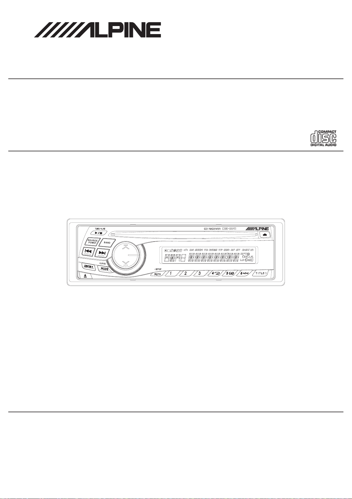
FM/AM CD Receiver
(CDE-9841)
2 / 05-A
68E38344S01
CDE-9841/CDE-9841E
Page 2
<Cautions for Safe Repair Work>
r
s
- 2 -
The following cautions will prevent accidents in the workplace and will ensure safe products.
*The symbols indicate caution is needed to prevent injuries and damage to property.
The symbols and their meanings follow.
Warning
Caution
*The following symbols indicate two levels of cautions.
When you see this symbol, you have to be very careful.
When you see this symbol, you have to follow the instructions there.
If you ignore this symbol and handle the product incorrectly or unsafely,
serious injury or death may result.
If you ignore this symbol and handle the product incorrectly or unsafely,
injury or only material damage may result.
Warning
Do not look squarely into the laser light
coming from the pickup. Always use a designated fuse.
You may loose you sight. Use of an incorrect fuse may result in a fire.
Caution
Do not allow wiring to be caught in the Battery Caution
screw/chassis. Use the designated battery.
If wiring is caught in the screw/chassis, it may Confirm the correct polarity and seat of the
cause a short circuit, resulting in a fire. battery.
Fuse Caution
An incorrect battery or an improperly connected
or seated battery may result in a fire.
High Temperature Caution Designated Parts Caution
Touching the heat sink may cause severe burns. Look up the part list and ensure that only
designated parts are used to prevent problems or
accidents.
Reverse Power Supply Connections o
Misconnections Caution Ensure that the wiring is correct when rewiring to
Reverse power supply connections or prevent problems with ignition/breakdown.
misconnections may cause ignition problems and
smoke may result.
Soldering Caution Wear Glove
Hot solder from solder splash may cause severe Wear gloves to prevent electrical shocks or injury
burns. from the end face of the metal.
Wiring Caution
Page 3

Contents
- 3 -
CDE-9841/CDE-9841E
Packing Assembly Parts List
Packing Method View
Specifications
5, 6
Extension Cable
Block Diagram
Parts Layout on P.W.Boards and Wiring Diagram
Schematic Diagram
Terminal Voltage of IC/TR
Description of IC Terminal
9 to 13
14 to 19
20 to 25
26 to 30
Exploded View (Cabinet)
Exploded View (CD Deck Mechanism) (DP23S87T)
4
4
7
8
31
32
NOTE : Due to continuing product improvement, specifications and designs are subject to
change without notice.
Page 4
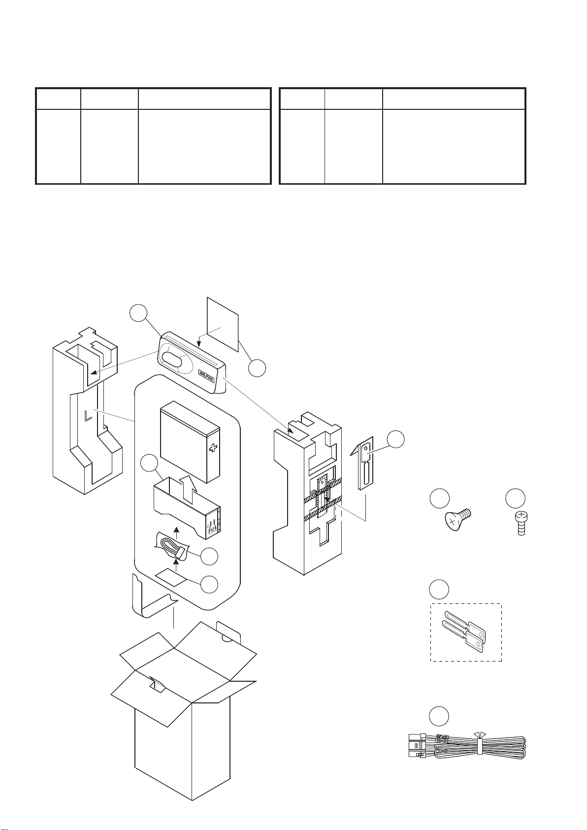
Packing Assembly Parts List
- 4 -
TO CONTENTS
CDE-9841/CDE-9841E
Symbol SymbolDescription
Part No. Part No.
Description
No. No.
101 15-01970Z01 CASE,INNER
102 15D01798K03 CARRYING,CASE
103-1 03S60820Y16 SCR,MCH 5X8 ZN A
103-2 03S60824Y01 SCR,WEV 1.7X4 ZN A
104 07-01964Z01 BKT,RELEASE
NOTE: #2:For CDE-9841 Model Only, $2:For CDE-9841E(General Foreign) Model Only, %2:For CDE-9841E(Chinese) Model Only,
Others:Common.
105 09-02256Z01 ASSY,ANIC-0008-01A
#2
105 09-01538Z05 ASSY,POWER WIRE9841E
$2
105 09-01538Z05 ASSY,POWER WIRE9841E
%2
106 68-00493Z95 O/M AOAM AOTA
#2
106 68-02278Z05 O/M AAO AODN
$2
106 68-02770Z01 O/M,AOCH 9841
%2
Packing Method View
102
106
101
BO
TTOM
Side
105
103
104
103
104
105
X2
103
-2
X1
-1
X4
X1
Page 5

CDE-9841/CDE-9841E
- 5 -
TO CONTENTS
Specifications
< FM RADIO >
Intermediate Frequency ........................................................................................................................ 10.7±0.1MHz
Frequency Range .................................................................................................................... 87.7 to 107.9MHz (#1)
87.5 to 108.0MHz ($1)
Usable Sensitivity (3% Dist., Mono, at 98.1MHz) ........................................................................................... 20.2dBf
Quieting Sensitivity (50dB S/N, Mono, at 98.1MHz) ....................................................................................... 20.2dBf
-3dB Limiting Sensitivity (at 98.1MHz) ........................................................................................................... 20.2dBf
Residual Noise (Ref. 400Hz, at 98.1MHz) .................................................................................................... 30±10dB
S/N Ratio (at 98.1MHz) ......................................................................................................................... Stereo : 55dB
Mono : 60dB
Image Rejection (at 106.1MHz) .......................................................................................................................... 40dB
IF Rejection (at 90.1MHz) .................................................................................................................................. 60dB
Distortion (Input 60dBu, at 98.1MHz) ................................................................................................................. 1.5%
Frequency Response (Ref. 400Hz, at 98.1MHz) ................................................................................ 100Hz : 0±3dB
10kHz : -13±3dB
Stereo Separation (1kHz, at 98.1MHz) .............................................................................................................. 20dB
< AM RADIO >
Intermediate Frequency ....................................................................................................................... 1st : 10.8MHz
2nd : 450kHz
Frequency Range ...................................................................................................................... 530 to 1,710kHz (#1)
531 to 1,602kHz ($1)
Usable Sensitivity (20dB S/N, at 1,000kHz(#1), 999kHz($1)) ............................................................................ 35dB
S/N Ratio (at 1,000kHz(#1), 999kHz($1)) .......................................................................................................... 44dB
Image Rejection (at 1,400kHz(#1), 1,404kHz($1)) ................................................................................ 2nd IF : 40dB
IF Rejection (at 600kHz(#1), 603kHz($1)) ............................................................................................. 2nd IF : 60dB
Distortion (at 1,000kHz(#1), 999kHz($1)) ........................................................................................................... 1.5%
Frequency Response (Ref. 400Hz, at 1,000kHz(#1), 999kHz($1)) .................................................... 100Hz : -3±4dB
4kHz : -14±6dB
< CD SECTION >
System ....................................................................................................................... Optical (Compact Disc System)
Channel Balance (1kHz) ................................................................................................................. TCD-782 : 0±3dB
Distortion (1kHz) ................................................................................................................................ TCD-782 : 0.3%
Frequency Response (Ref. 1kHz, 0dB) ............................................................................... TCD-782 : 17Hz : 0±3dB
127Hz : 0±2dB
10.007kHz : 0±2dB
19.997kHz : -1±4dB
S/N Ratio ........................................................................................................................................... TCD-782 : 85dB
Separation (1kHz) ............................................................................................................................. TCD-782 : 55dB
De-Emphasis (Ref. 1kHz, 0dB) ........................................................................................ TCD-782 : 4kHz : -20±3dB
16kHz : -20±3dB
NOTE : #1 : For CDE-9841 Model Only, $1 : For CDE-9841E Model Only, Others : Common.
Page 6

CDE-9841/CDE-9841E
- 6 -
TO CONTENTS
< CD Deck Mechanism >
Test Disc ....................................................................................................................................................... TCD-782
RF Waveform Amplitude .......................................................................................................................... 1.0±0.5Vp-p
Quantity of Jitter ............................................................................................................................. Less than 30nsec
Measurement Angle Range ............................................................................................... Front and Rear : -15°~75°
Right and Left : ±45°
Laser Current ................................................................................................................................. Initial value ±5mA
(The initial value of laser current is indicated on the Flexible Cable.)
< Pickup >
Wave Length .................................................................................................................................................... 795nm
Laser Power .................................................................................................................................................. CLASS I
< GENERAL >
Power Supply ............................................................................................................................................... DC14.4V
Power Output (FM 98.1MHz, Mod.1kHz, T.H.D.1%) / Impedance ........................................... 16W / ch / 4 ohm (#1)
(TCD-782 (1kHz, 0dB), T.H.D. 10%) / Impedance ............................................ 16W / ch / 4 ohm ($1)
Pre Output (TCD-782 (1kHz, 0dB), T.H.D. 1%) / Impedance ............................................ 6 +3/-2dBV / ch / 10k ohm
Back Up Current .................................................................................................................................................. 5mA
Dimensions (W x H x D) ................................................................................................ Chassis : 178 x 50 x 162mm
Nose : 188 x 58 x 18mm
Weight ................................................................................................................................................................ 1.6kg
NOTE : #1 : For CDE-9841 Model Only, $1 : For CDE-9841E Model Only, Others : Common.
: Due to Continuing product improvement, specifications and designs are subject to change without notice.
Page 7
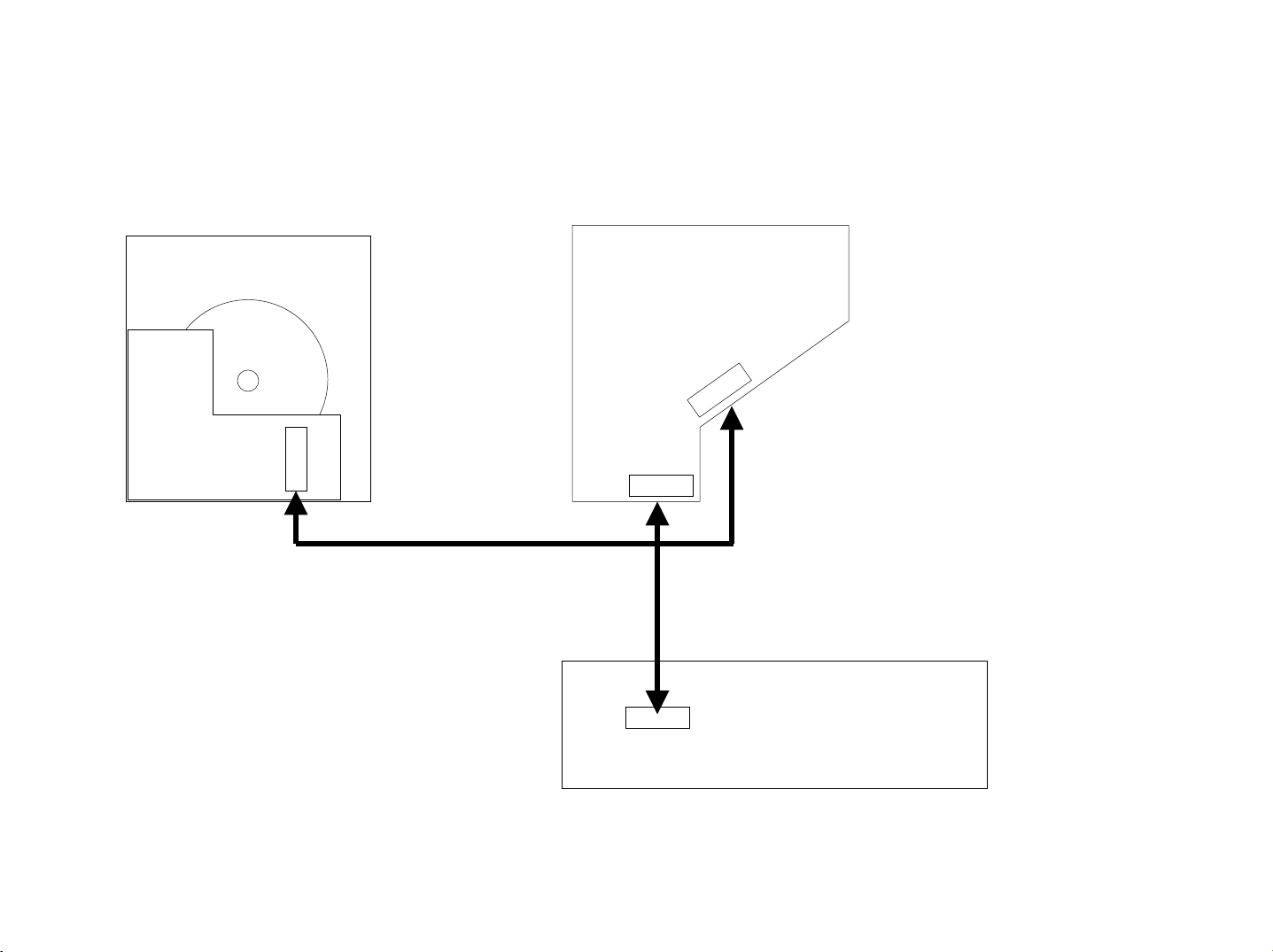
Extension Cable
- 7 -
TO CONTENTS
*Always connect the Extension Cable when making checks of voltage and repair.
CD Deck Mechanism
DP23S87T
MAIN P.W.Board
1
0
1
B
C
CDE-9841/CDE-9841E
CB801
CB501
(1)
(2)
CH401
FRONT P.W.Board
(1) 01E29616S01
(2) 01V37775S01
Page 8
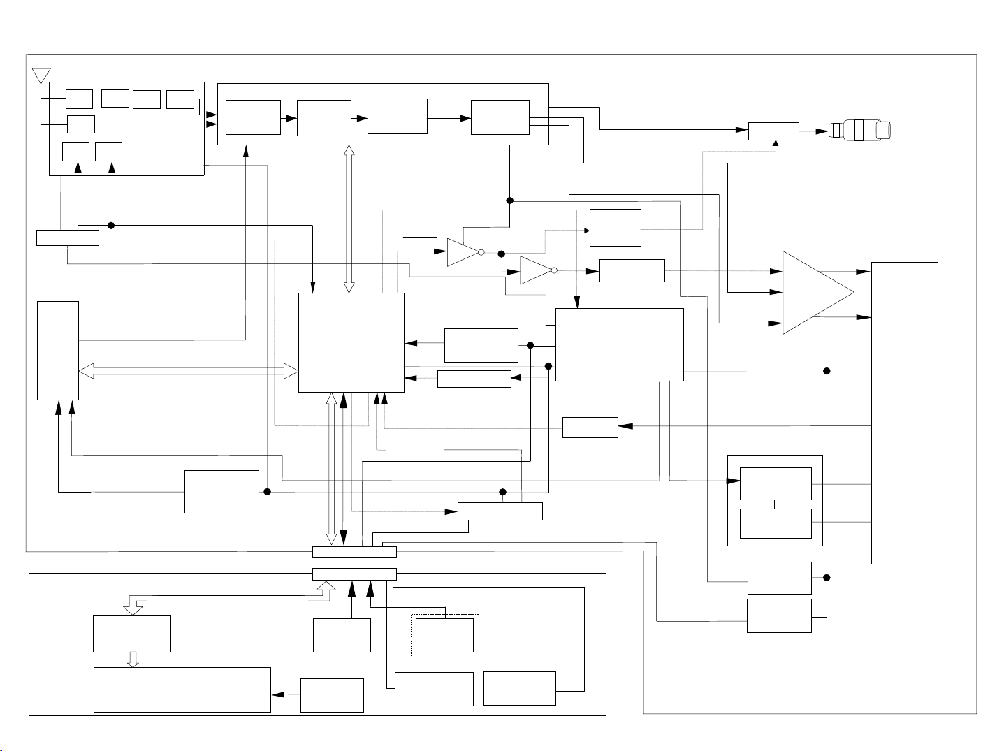
Block Diagram
- 8 -
TO CONTENTS
Tuner unit
E2P
ROM
Tuner on
N.C. MPX
RF IF
AM
PLL
TUNER+B
(CD MECH)
DP23S87T
Selector
CD
Vol.1
Main CPU
Tre/Bass
A-Mute
E-VOL
RESET
BAT DET SW
Vol.2
MUTE
DRIVER
Delay Circuit
Power cont
SYSTEM POWER IC
Batt-Det / VDD
PWR-ON / CD SERVO
TUNER ON
CDE-9841/CDE-9841E
MUTE
Front
Power IC
Rear
BATT
Pre-OUT
SubWoofer/Front
LCD DRIVER
LCD
DISPLAY
VDD+5V
VDD
Key Input
A/D
LCD+B
Nose DET
Remote
Control
Nose
Light
Nose PWR SW
CDE-9841E
Model Only
LCD
Light
ACC DET
CD-SERVO
PWR ON
PWR ANT
Rem SW
AUDIO +B
LED +B
ACC
POWER CONNECTOR
P.ANT
O.REM
Page 9
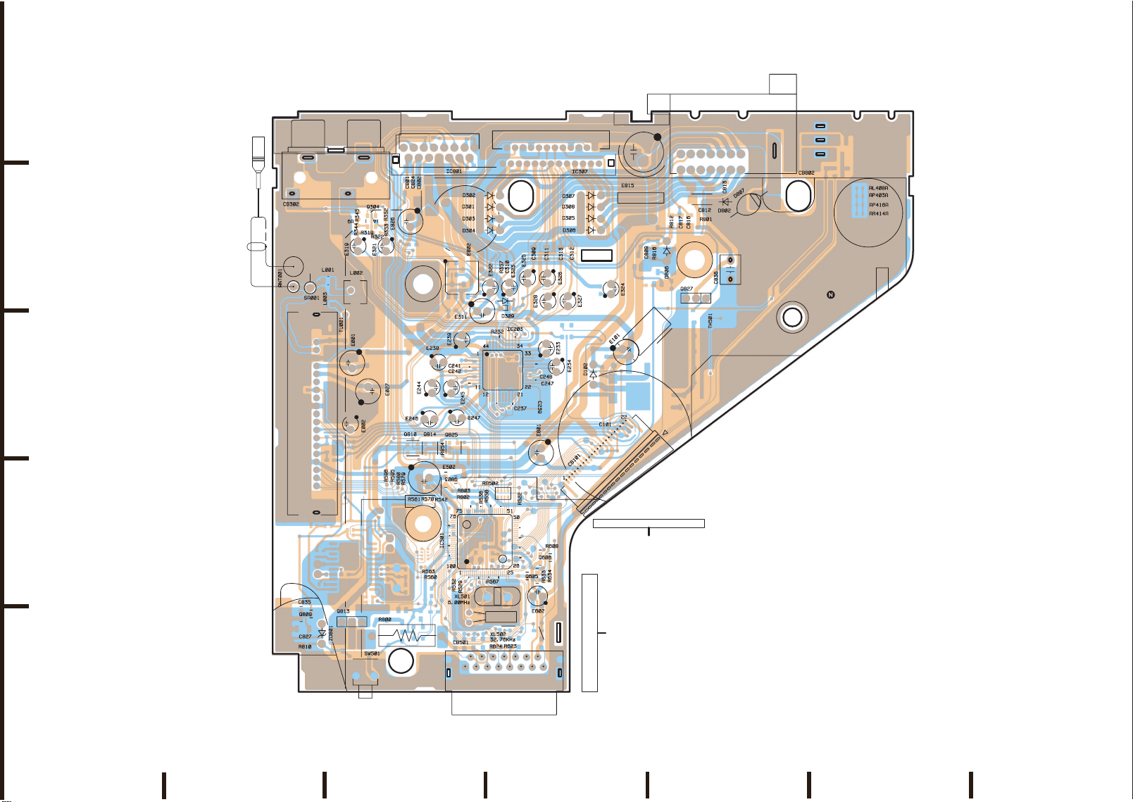
Parts Layout on P.W.Boards and Wiring Diagram(1/5)
- 9 -
TO CONTENTS
MAIN P.W.Board
1
(Component Side View)
JK581
CDE-9841/CDE-9841E
2
4
5
3
ANT001
2
ASSY,ANT CABLE 9805A
BLK
(ANT)
SHIELD
WHT
ANT001
C835
Q809
B
E
R809
C827
R810
L001
SA001
TU001
1
19
C054
R028
E051
C051
L003
C055
C057
ZD801
34
1
CB302
46
R345
R344
E319
L002
E001
E002
R057
R056
IC052
R063
C059
EB
Q813
SW501
Q304
R319
E027
R055
13
R322
C052
R059
R352
R353
E321
E052
IC801
R596
R595
XL051
1
C801
Q810
R580
R579
C824
E826
C011
R561
C802
3512
E244
Q814
12
R578
RA503
R562
R563
R560
35
E502
R542
E246
E238
E245
Q825
R854
53
B
E
R800
C241
C242
21
Q803
R532
E802
E239
R803
R529
XL502
8
142
E247
R802
15
R536
IC501
D302
D301
D303
E322
E311
R556
R567
IC307
D304
R232
IC203
XL501
R624
24
C310
R357
E323
RA502
R623
D309
C237
R522
E325
Q605
E602
C309
C248
B
E
E
B
2
125
D307
D308
D305
D306
C313
C312
C311
E326
E233
C239
E801
R608
Q606
R634
R633
915
E328
C247
1
E234
CB501
E324
E327
D102
C101
1
CB10
From DP-S MAIN P.W.Board (CB801)
18
To CB501
15 9
From FRONT P.W.Board (CH401)
E815
C809
C109
1
E10
To CB101
R816
D806
R812
8
16
C817
C816
B E
221
D808
D802
C812
R801
Q827
TH501
C813
C836
1
CB802
9
D807
R544
R545
R547
R546
A
Orange Color Pattern:Component Side Pattern
Blue Color Pattern:Foil Side Pattern
FGEDCB
Page 10
Parts Layout on P.W.Boards and Wiring Diagram(2/5)
- 10 -
TO CONTENTS
CDE-9841/CDE-9841E
1
2
4
3
Q582
R584
R582
R589
C583
C582
MAIN P.W.Board (Foil Side View)
C811
C814
R602
C601
D601
R604
Q601
R847
R850
R849
R853
R852
R851
B
E
Q828
NOTE : #1 : For CDE-9841 Model Only,
$1 : For CDE-9841E Model Only,
Others : Common.
3
IC101
C308
1
23
Q101
5
R101
C102
1
C103
D101
R804
R855
R065
E
R064
Q815
C560
C318
D001
R002
R043
C001
C010
C012
C061
C062
R819
R828
R813
B
R807
R814
R571
C053
R808
R034
C040
R033
C039
R036
R031
R032
C058
R829
C825
C826
C806
C307
Q307
R355
E
R362
C253
B
Q201
R558
R612
$1
E
TP506
TP504
R613
TP508
TP507
TP503
R614
#1
C505
R615
C506
R518
C504
C503
C507
R616
C240
C243
C255
C256
R552
R551
TP509
TP502
R617
$1
R566
TP501
R618
R231
TP505
R534
$1
$1
R605
R635
R607
R609
C805
C804
B
B
TP510
R619
C810
1
Q306
5
E
Q305
R550
C803
32
R361
Z502
R570
R569
D803
C508
D801
C561
1
IC560
5
23
5
A
Orange Color Pattern:Component Side Pattern
Blue Color Pattern:Foil Side Pattern
FGEDCB
Page 11

Parts Layout on P.W.Boards and Wiring Diagram(3/5)
- 11 -
TO CONTENTS
1
CDE-9841/CDE-9841E
2
4
3
R473
D407
C407
R434
SW414
LD403
LD404
$1
B
Q401
E
$1
R433
LD433
$1
SW412
LD435
SW416
R404
R436
R437
R423
LD410
LD420
LD432
LD436
SW415
R439
R411
SW411
R435
R432
R431
SW410
LD409
LD405
SW413
R440
LD422
R471
R447
FRONT P.W.Board
(Component Side View)
SW418
LD423
LD419
LD401
SW409
SW408SW407SW406SW405SW404SW403SW402
R430R429R428R427R426R425R424
LD424
SW419
LD415 LD414
FRONT P.W.Board (Foil Side View)
To MAIN P.W.Board (CB501)
1 8
D403
D401
R403
R441
R446
IC401
ZD401
C404
C402
C403
R402
R401
C401
R438
D404
C405
To CH401
D402
$1
R442
R422
R417
CH401
LD407 LD406
R405
D406
R421
R419
C406
159
R456
R420
LD412 LD411
NOTE : $1 : For CDE-9841E Model Only,
R455
R444
R445
LD418 LD417 LD416
Others : Common.
R443
R453
R413
R414
R406
R407
LCD401
SW401
LD408
1
4
$1
IC402
23
LD402
LD413
R479
R474
R475
R476
R477
R478
5
A
Orange Color Pattern:Component Side Pattern
Blue Color Pattern:Foil Side Pattern
FGEDCB
Page 12

Parts Layout on P.W.Boards and Wiring Diagram(4/5)
- 12 -
TO CONTENTS
1
FPC CONT P.W.Board
(Foil Side View)
DP-S Main P.W.Board
(Foil Side View)
CDE-9841/CDE-9841E
2
4
3
TP106
TP109
TP101
TP108
TP92
TP91
TP13
TP12
C140
TP102
TP93
Q101
E102
Q107
Q106
E111
TP95
TP94
CB801
TP97
TP104
TP110
TP111
TP112
TP52
TP96
TP99
TP98
TP105
TP103
C102
R105
E112
R107
E103
E203
E110
IC201
IC203
TP89
C104
R121
TP11
E113
TP100
C141
TP88
C105
C112
C111
C110
C108
C205
CB101
R103
R102
R120
R118R119
E104
TP107
IC104
E202
TP90
E201
R101
R104
R116
Q103
R171
C210
R172
E101
C125
C126
R168
C101
Q102
R106
E108
C121
C127
TP30
R108
R113
TP26
C122
R110
TP25
IC102
TP113
TP114
TP22
TP82TP81
TP83
R134
TP115
TP24
TP33TP32TP31
R166
C144
R167
C209
R170
XL101
C146
R173
CL102
TP61TP66 TP65
TP73TP72TP71TP70TP69TP68TP67
TP62
C123
R162
TP80
TP60
C120
TP58
TP59
R112
R111
C139
IC101
TP85
E107
C153
TP19
TP78
C124
TP77
R177
TP20
TP86
C147
E105
C129
C128
C109
R109
R178
C136
TP23
TP18
R133
R141
C133
C134
C132
R132
R130
R124
R129
TP21
TP29
R163
C131
E106
TP63
TP64
R157
C149
R159
C150
R123
C114
CB102
IC103
IC303
C115
C300
R313
C307
R305
C302
IC300
R314
R302
C306
IC302
C303
R306
R304
R300
DP-S Switch P.W.Board
(Foil Side View)
R301
C309
C311
R309
C305
5
A
Orange Color Pattern:Component Side Pattern
Blue Color Pattern:Foil Side Pattern
FGEDCB
Page 13

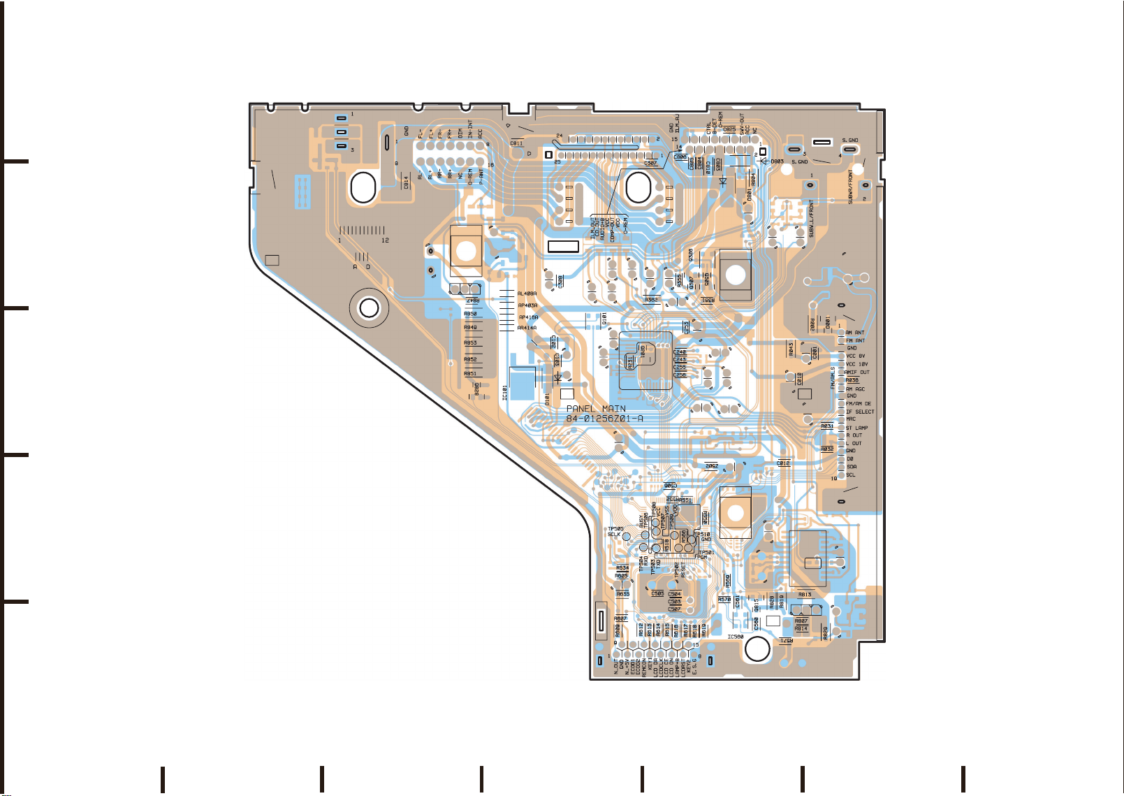
Parts Layout on P.W.Boards and Wiring Diagram(5/5)
- 13 -
TO CONTENTS
1
DP-S Main P.W.Board
(Component Side View)
CDE-9841/CDE-9841E
2
4
3
C310
R158
R315
R311
C312
IC301
4513
C304
TP14
TP15
TP16
R154
R152
R131
R150
R149
D101
TP17
R310
R128
C113
Q105
1
R151
5
TP76
R127
2
3
R153
R161
C135
R165
R126
R156
C137
C138
R164
R125
R155
R160
R115
R114
TP84
TP54
R122
R185
TP56
TP55
R182
R179
R187
R174
R186
R191
TP57
TP4
TP2
TP1
C106
C145
R169
C151
C148
TP3
R183
C143
R219
TP27TP28
R181
C142
R220
TP10
R180
R218
C208
R204
R203
TP8
TP5
R184
TP46
R208
C204
C207
R217
TP9
TP7
TP6
R206
R212
C203
R205
R207
C202
R210
R211
R209
C201
R214
R213
TP53
TP39
TP45
TP42
TP41
TH101
TP40
TP47
TP44
TP43
R188
R189
R190
TP75
TP74
TP51
TP36
C157
TP35
C156
TP34
C155
TP48
TP49
TP50
TP37TP38
5
A
Orange Color Pattern:Component Side Pattern
Blue Color Pattern:Foil Side Pattern
FGEDCB
Page 14

R551
- 14 -
TO CONTENTS
TO PARTS LIST
TO P. W. BOARD
R552
$1:10k
#1:N.U.
$1:N.U.
#1:10k
4.7k
47k
47k
4.7k
R580
R596
R579
R595
R542
100
100
R578
R561
1k
RA503
N.U.
R562
N.U.
R563
100
R560
1k
15k
R550
TH501 100k
1k
R536
IC501
M30624FGPGP
1k
R556
1k
RA502
R570
R534
#1:N.U.
$1:0
R522
1k
R558
N.U.
R569
3.9k
27k
R589
N.U.
N.U.
C582
N.U.
R582
Q582
N.U.
N.U.
R584
JK581
N.U.
N.U.
C583
R532
470k
2.7k
Q605
2SA1037AK
100k
R634
10k
10k
0.1
C560
2.2k
Q606
DTC124EKA
R613
IC560
R633
BD5228G
Z502
C561
0.047
27k
22k
R608
10k
R607
1k
10k
R609
CB501
BTB, DF15-S
BK2125HM102
N.U.
C506
C508
1k
R612
$1:1k
#1:N.U.
0.02225V
E502
330/6.3
R800
12
1k
R619
R614
R616
1k1k1k
1k
R618
R617
R615
XL502
18p
C503
32.76kHz
XL501
47k
R567
27p
20p
27p
6.00MHz
C507
C504
C505
R518
47k
TP502
TP501
TP509
TP510
TP508
TP507
TP504
TP506
TP503
TP505
1k
22k
R566
R529
R571
SW501
SW ,TACT SKHHLW
22/16
R635
E602
R605
#1:N.U.
$1:22k
R623
R624
Page 15

10/16
- 15 -
TO CONTENTS
TO PARTS LIST
TO P. W. BOARD
E234
10/16
E233
C247
C248
1000p
1000p
R231
33k
C239
1000p
C237
1000p
C253
E239
4.7/35
0.1
16V
R232
10k
Q201
DTC124EKA
IC203
BD3426K
1000p
1000p
1000p
1000p
10/16
E238
10/16
0.01
10/16
0.01
4.7/35
E247
E246
E245
C240
C242
C256
E244
C243
C255
C241
4.7/35
CB302
RCA, NLT1987-0
E319
2.2/50
2.2/50
R344
220
Q304
XN0F256
56k
R319
56k
R322
E321
R353
220
R345
R352
100
100
N.U.
C318
Page 16

Q827
- 16 -
TO CONTENTS
TO PARTS LIST
TO P. W. BOARD
2SB1243
24k
R855
N.U.
D808
N.U.
C825
0.22
16V
4.7k
Q803
DTC143EKA
R802
C826
N.U.
4.7k
R803
50V
0.27
C836
10k
R801
D802
S1G-6904
Q825
FMC3A
IC801
HA13165
R804
C835
30k
0.022
C801
D803
S1G-6904
0.1
16V
C824
E802
220/10
0.22
16V
S1G-6904
D801
C810
C803
C804
C805
C806
C802
E826
470/10
220/6.3
E801
0.47
25V
0.1
16V
0.1
16V
0.22
16V
0.1
16V
0.1
16V
R853
Q828
DTC123JKA
1.6k
1.6k
R849
R847
1.6k
1.6k
1.6k
R851
R852
R850
D309
1SS355
DTC114EKA
Q305
R362
100
10k
R361
Q306
FMC2A
E311
1/50
E325
1/50
E326
1/50
E327
1/50
E328
47/16
Q307
DTC124EKA
C309
C311
C312
C313
R355
330
IC307
TA8263BH
1/50
E322
C307
1000p
50V
10/16
E323
E324
C310
0.22
0.22
0.22
0.22
10k
R357
C308
0.22/50
0.22
16V
0.047
16V
SRT14
SRT14
SRT14
SRT14
D302
D301
D303
D304
SRT14
SRT14
SRT14
SRT14
D305
D307
D308
D306
R829
R814
R810
R807
2.2
47k
R808
N.U.
27k
Q813
2SB1243
2.2
R828
2.2k
Q815
DTC143XKA
10k
R813
2.2k
R819
E815
C811
0.022
3300/16
CB802
ASSY, W277A001
D807
C814
0.01
0.01
C813
C816
0.01
C817
0.01
0.01
C812
DSA3A4
ZD801
Q809
DTC124EKA
Q810
FMC2A
Q814
FMC3A
100k
R854
Q601
N.U.
D601
N.U.
N.U.
R604
D806 MA165-(QZ)
C601
R812
6.8k
C809
3.3k
R816
0.1 16V
R602
N.U.
N.U.
HZS6C3L
C827
N.U.
0.1 16V
R809
Page 17

CB101
- 17 -
TO CONTENTS
TO PARTS LIST
TO P. W. BOARD
SFW22R-1STE1
D101
S1G-6904
IC101
AN7705SP
TU001
MX-A196
C109
C103
Q101
FMC3A
N.U.
SA001
ANT001
ASSY, ANTCABLE9805R
C001
R036
33k
N.U.
C039
25V
0.047
E002
R031
R032
N.U.
C040
DSP-201M
L001
4.7u
L002
33mH
15u
L003
10
R002
D001
1PS226
25V
E001
E027
C010
0.047
100/16
4.7/35
3.3k
3.3k
100/16
N.U.
N.U.
R033
R034
R043
4.7
N.U.
C011
0.01
C012
0.01
0.1
C102
D102
11ES2N-TB5
IC052
N.U.
R064
N.U.
N.U.
N.U.
N.U.
E051
C058
C059
N.U.
R063
XL051
N.U.
N.U.
N.U.
C061
C053
N.U.
C055
N.U.
N.U.
R028
C051
N.U.
N.U.
C057
C054
E052
C052
C101
0.022 25V
N.U.
N.U.
R055
N.U.
N.U.
R065
N.U.
C062
N.U.
E101
R101
470/10
N.U.
N.U.
R056
R057
R059
N.U.
Page 18

D406
- 18 -
TO CONTENTS
TO PARTS LIST
TO P. W. BOARD
D401
D402
D403
D404
LCD401
LCD, GTD-22608AAHK-CU
1PS226N.U.
1PS226
750
R406
82
82
R403
R404
R407
3.9k
LD403
LD401
NSCW505CT
Q401
2SD601A
SML-310LT
LD402
NSCW505CT
1PS2261PS226
R419
1k
470
R417
R405
R421
470
330
R413R414
LD420
R443
1.5k-1/4
LD410
1.5k-1/4
GRN 310PT-KL
LD405
GRN UG1104B
GRN 310PT-KL
LD409
GRN 310PT-KLGRN 310PT-KL
LD404
220
R444
220
R445
LD422
LD414
LD415
220
R441
220
R446
LD416
GRN 310PT-KL
GRN 310PT-KL
GRN 310PT-KL
GRN 310PT-KL
LD411
GRN 310PT-KL
LD406
GRN 310PT-KL
220
R456
220
R455
LD424
GRN 310PT-KL
LD423
GRN 310PT-KL
LD419
GRN 310PT-KL
220
R440
220
R447
LD417
GRN 310PT-KL
GRN 310PT-KL
LD412
GRN 310PT-KL
LD407
GRN 310PT-KL
4.7k
C405
R438
0.022 24k
220
R439
220
R411
LD418
GRN 310PT-KL
LD413
GRN 310PT-KL
LD408
GRN 310PT-KL
N.U.
R453
C406
N.U.
LD436
N.U.N.U.
LD435
LD433
N.U.
LD432
470
R422
CH401
R420
24k
0.022
BTB, DF15-P
IC401
PT6523LQ
C402
C403
R401
C401
0.047
0.047
1000p
47k
ZD401
RD5.1MB1
100k
R402
C404
0.047
R423
1.3k
SW401
SKRPACE010E2
R431
1.3k
SW410
SKRPACE010E2
R424
1.8k
SW402
SKRPACE010E2
R432
1.8k
SW418
SKRPACE010E2
R433
2.2k
R426
R434
SW412 SW413
R425
2.2k
SKRPACE010E2
SW411
SKRPACE010E2 SKRPACE010E2
3.3k
R427
4.3k
SW405SW404SW403
SKRPACE010E2
SKRPACE010E2SKRPACE010E2
R435
3.3k
4.3k
SW414
SKRPACE010E2
SKRPACE010E2
R429R428
7.5k
SW407SW406
SKRPACE010E2
R436
7.5k
SW415
SKRPACE010E2 SKRPACE010E2
R430
R437
15k
39k
SW408
SKRPACE010E2
SW416 SW419
R471
39k
SW409
SKRPACE010E2
SKRPACE010E2
15k
R424
#1:N.U.
$1:1k
R473
#1 :N.U.
$1 :100
D407
#1 :N.U.
$1 :1PS226
IC402
C407
$1 :4.7
#1:N.U.
$1:RS-671
#1 :N.U.
Page 19

HD101
- 19 -
TO CONTENTS
TO PARTS LIST
TO P. W. BOARD
PICKUP,
EP21A65T
52207-1590
52207-0790
SW105
SPPB12016B
CB101
CB102
FMG1
TP5
TP76
Q102
TP37
TP103
TP104
TP105
C201
IC203
820p
R207
15k
C203
C204
R208R206R218
15k
10/16
TP39
TP38
TP40
TP36
TP35
TP34
N.U.
NJM2100M
R209
270p
1.1k
240k
R211
R212
270p
C202
820p
E113
100
R185
R186
TP111
TP110
22/6.3
240k
R210
1.1k
IC203
NJM2100M
100
R179
100
R180
100
R181
R182
R183
100
100
R187
TP112
R213
N.U.
E203
C205
R214
TP63
TP64
100
100
100
R184
TP74
47
TP91
TP75
47
TP92
TP93
M101
ASSY, MOTOR-WORM
TP65
TP66
TP67
TP68
TP69
TP70
TP71
TP72
TP73
TP61
TP62
SPVG11
SW1
SW2
SW4
SPVG21
SW3
SPVG21
SPVG21
TP94
TP95
TP96
TP97
TP98
TP99
TP100
TP101
TP51
TP52
TP53
CB801
52207-2290
TP88
TP25
R110
56k
C122
160p
R108
100
0.1
C121
R106
TP30
47k
Q103
FMG1
AN8882SB
C105
3900p
20k
IC102
TP11
10k
0.022
10/16
47/5.5
E103
E110
C104
R131
C113
0
N.U.
R150
R149
390k
820
51k
R151
R301
180k
Q105
FMC2
R118
1
4.7/35
0.027
4700p
0.027
C110
C108
C109
C106
E104
R125
47k
R126
30k
R127
51k
R128
2.7k
R129
390k
R130
47k
470p
C311
R311
47k
C115
E106
10/16
0.022
R153
33k
TP4
TP1
TP2
TP3
47k
R116
TP7
TP6
R101
R102
11k
0
TP9
TP8
TP10
R103
R104
0
11k
Q101
2SB1132
C101
0.022
12
R107
47/5.5
0.047
E101
10
R105
R123
10/16
E102
TP18
C102
R124
10018k
IC103
BA5985FM
TP19
D101
MA159
R152
10k
R154
10k
R120
5.1k
R121
R158
TP13
TP12
TP15
TP16
TP17
TP14
C149
180p
R157
22k
C150
15k
1500p
R159
10k
R111
0
R112
10k
TP26
R113
56k
TP27
TP28
68p
C123
10/16
0.1
0.022
E107
C124
C126
E108
10/16
TP114
20k
R119
2200p
C111
R132
0
E105
N.U.
220k
R315
R134
330p
TP23
TP22
R155
100
R156
IC301
0.1
TP24
100
R133
1k
C114
6800p
C304
0.022
TC7S66FU
N.U.
IC303
R313
C112
C312
0.1
C127
C125
5600p
R122
10k
2.2k
TP113
TP21
R141
C307
TC7SH08FU
R114
R115
220k
240k
N.U.
1800p
TP29
C128
C129
C120
560p
TP20
100
39k
R300
0.01
C300
TC7WH123FU
0.022
IC302
C305
0.022
C310
470p
22k
R310
0.1
C153
47k
R109
C139
0.022
TP115
R306
10k
R305
IC300
0.1
C306
C303
10k
0.033
0.1
C302
NJM2100V
R314
R304
R309
47k
3.3k
C309
1k
2.2
R302
47k
C138
C137
100p
C132
C131
TP77
R160
TP80
TP81
TP82
TP83
TP31
TP32
TP33
0
R161
2.7k
0.22
TP78
R162
220k
Q106
DTB113EK
DTC124EUA
0.1
120k
N.U.
0.1
C133
R178
0.1
C141
Q107
0.022
C134
470
R163
TP86
IC104
TC74VHCT08AFT
1M
0.022
C135
R165
R164
100k
IC101
MN662771AW
100
100
R168
R166
C142
R167
C143
100
C144
100
R169
C145
N.U.
N.U.
N.U.
N.U.
XL101
16.93MHz
E111
C140
47/5.5
C209
0.022
0.022
C136
R170
47k 47k
270
R171
18p
C210
18p
R172
C146
R173
0.1
0
CL102
4.19MHz
TP90
240k
R219
R220
C147
0.022
TP58
TP59
TP60
TP84
47k
R191
33k
R174
240k
R177
8.2k
TP89
TP85
C151
R190
TH101
C148
1000p
100
R217
R205
2.2k
6.2k
16k
R203
150p
C207
E201E202
22/6.3
22/6.3
150p
C208
16k
R204
2.2k
6.2k
IC201
NJM78L05UA
100k
E112
22/6.3
0.01
TP54
TP55
TP56
TP57
TP45
TP46
TP47
TP48
TP49
TP50
TP41
TP102
TP42
TP43
TP44
TP107
TP108
TP106
TP109
R188
R189
100
100
N.U.
N.U.
C157
C155
C156
M103
M102
ASSY, MOTOR SLEDASSY, MOTOR SLED
ASSY, MOTOR SPINDLE
Page 20

CDE-9841/CDE-9841E
- 20 -
TO CONTENTS
TO SCHEMATIC
Terminal Voltage of IC/TR
REF NO. HIGH(V) LOW(V) REF NO. HIGH(V) LOW(V)
1 7.0(CD) 0(TUNER) 1 0(POW ON) 0(POW OFF)
IC101
REF NO. HIGH(V) LOW(V) 6 14.4(POW ON) 14.4(POW OFF)
IC203
2 0.6(CD) 0.2(TUNER) 2 0(POW ON) 0(POW OFF)
3 5.6(CD) 0.2(TUNER) 3 7.6(POW ON) 0(POW OFF)
4 4.8(POW IC ON) 0(POW IC OFF)
5 7.6(POW ON) 0(POW OFF)
1 0(POW ON) 0(POW OFF) 7 7.6(POW ON) 0(POW OFF)
2 4.3(POW ON) 0(POW OFF) 8 0(POW ON) 0(POW OFF)
3 4.3(POW ON) 0(POW OFF) 9 7.6(POW ON) 0(POW OFF)
4 4.3(POW ON) 0(POW OFF) 10 9.0(POW ON) 0(POW OFF)
5 4.3(POW ON) 0(POW OFF) 11 1.4(POW ON) 0(POW OFF)
6 4.3(POW ON) 0(POW OFF) 12 1.4(POW ON) 0(POW OFF)
7 4.3(POW ON) 0(POW OFF) 13 0(POW ON) 0(POW OFF)
8 4.3(POW ON) 0(POW OFF) 14 1.4(POW ON) 0(POW OFF)
9 4.3(POW ON) 0(POW OFF) 15 1.4(POW ON) 0(POW OFF)
10 4.3(POW ON) 0(POW OFF) 16 1.4(POW ON) 0(POW OFF)
11 4.3(POW ON) 0(POW OFF) 17 7.6(POW ON) 0(POW OFF)
12 4.3(POW ON) 0(POW OFF) 18 0(POW ON) 0(POW OFF)
13 4.3(POW ON) 0(POW OFF) 19 7.6(POW ON) 0(POW OFF)
14 4.3(POW ON) 0(POW OFF) 20 14.4(POW ON) 14.4(POW OFF)
15 4.3(POW ON) 0(POW OFF) 21 7.6(POW ON) 0(POW OFF)
16 4.3(POW ON) 0(POW OFF) 22 4.1(NORMAL) 0(MUTE)
17 4.3(POW ON) 0(POW OFF) 23 7.6(POW ON) 0(POW OFF)
18 4.3(POW ON) 0(POW OFF) 24 0(POW ON) 0(POW OFF)
19 4.3(POW ON) 0(POW OFF) 25
20 4.3(POW ON) 0(POW OFF)
21 4.3(POW ON) 0(POW OFF)
22 4.3(POW ON) 0(POW OFF) REF NO. HIGH(V) LOW(V)
23 4.3(POW ON) 0(POW OFF) 1 PULSE PULSE
24 4.3(POW ON) 0(POW OFF) 2 PULSE PULSE
25 4.3(POW ON) 0(POW OFF) 3 PULSE PULSE
26 4.3(POW ON) 0(POW OFF) 4 PULSE PULSE
27 0.7(POW ON) 0(POW OFF) 5 PULSE PULSE
28 4.3(POW ON) 0(POW OFF) 6 PULSE PULSE
29 4.3(POW ON) 0(POW OFF) 7 PULSE PULSE
30 4.3(POW ON) 0(POW OFF) 8 PULSE PULSE
31 4.3(POW ON) 0(POW OFF) 9 PULSE PULSE
32 4.3(POW ON) 0(POW OFF) 10 PULSE PULSE
33 4.3(POW ON) 0(POW OFF) 11 PULSE PULSE
34 4.3(POW ON) 0(POW OFF) 12 PULSE PULSE
35 4.3(POW ON) 0(POW OFF) 13 PULSE PULSE
36 4.3(POW ON) 0(POW OFF) 14 PULSE PULSE
37 4.3(POW ON) 0(POW OFF) 15 PULSE PULSE
38 4.3(POW ON) 0(POW OFF) 16 PULSE PULSE
39 4.3(POW ON) 0(POW OFF) 17 PULSE PULSE
40 8.6(POW ON) 0(POW OFF) 18 PULSE PULSE
41 8.6(POW ON) 0(POW OFF) 19 PULSE PULSE
42 PULSE PULSE 20 PULSE PULSE
43 PULSE PULSE 21 PULSE PULSE
44 0(POW ON) 0(POW OFF) 22 PULSE PULSE
IC307
IC401-1
Page 21

CDE-9841/CDE-9841E
- 21 -
TO CONTENTS
TO SCHEMATIC
REF NO. HIGH(V) LOW(V) REF NO. HIGH(V) LOW(V)
23 PULSE PULSE 1
24 PULSE PULSE 2
25 PULSE PULSE 3 4.8(POW ON) * 4.8(POW OFF) *
26 PULSE PULSE 4
27 PULSE PULSE 5
28 PULSE PULSE 6 0(POW ON) 0(POW OFF)
29 PULSE PULSE 7 0(POW ON) 0(POW OFF)
30 PULSE PULSE 8 0.7(POW ON) 0.7(POW OFF)
31 PULSE PULSE 9 0.7(POW ON) 0.7(POW OFF)
32 PULSE PULSE 10 4.9(NORMAL) 0(RESET)
33 PULSE PULSE 11 2.5(POW ON) 2.5(POW OFF)
34 PULSE PULSE 12 0(POW ON) 0(POW OFF)
35 PULSE PULSE 13 2.3(POW ON) 2.3(POW OFF)
36 PULSE PULSE 14 4.9(POW ON) 4.9(POW OFF)
37 PULSE PULSE 15 4.9(POW ON) 4.9(POW OFF)
38 PULSE PULSE 16 4.8(CD) 0(TUNER)
39 PULSE PULSE 17 4.9(NORMAL) 0(ACC OFF)
40 PULSE PULSE 18 4.9(POW ON) 4.9(POW OFF)
41 PULSE PULSE 19
42 PULSE PULSE 20
IC401-2
REF NO. HIGH(V) LOW(V) 45
IC402 *
* IC402 : For CDE-9841E Model Only 50 4.8( 0 MUTE) 0(ELSE)
43 PULSE PULSE 21
44 PULSE PULSE 22
45 PULSE PULSE 23 4.9(CD IN) 0(CD OUT)
46 PULSE PULSE 24 4.9(NOSE ON) 0(NOSE OFF)
47 PULSE PULSE 25 PULSE PULSE
48 PULSE PULSE 26
49 PULSE PULSE 27
50 PULSE PULSE 28
51 PULSE PULSE 29
52 PULSE PULSE 30
53 PULSE PULSE 31
54 PULSE PULSE 32
55 PULSE PULSE 33 PULSE PULSE
56 4.8(POW ON) 4.8(POW OFF) 34 PULSE PULSE
57 4.9(POW ON) 4.9(POW OFF) 35 PULSE PULSE
58 3.1(POW ON) 3.1(POW OFF) 36 4.9(CD) 4.9(TUNER)
59 1.5(POW ON) 1.5(POW OFF) 37 4.8(CD) 0(TUNER)
60 0(POW ON) 0(POW OFF) 38 PULSE PULSE
61 3.7(POW ON) 3.7(POW OFF) 39
62 PULSE PULSE 40 4.9(NOSE ON) 0(NOSE OFF)
63 PULSE PULSE 41
64 PULSE PULSE 42
1 4.6(CD) 4.6(TUNER) 46
2 0(CD) 0(TUNER) 47
3 4.6(CD) 4.6(TUNER) 48 4.9(POW IC ON) 0(POW IC OFF)
4 0(CD) 0(TUNER) 49 4.8(POW ON) 0(POW OFF)
IC501-1
43
44
51 4.8(NORMAL) 0(MUTE)
52
53 4.9(TUNER) 0(CD)
* PIN NO.3 : For CDE-9841E Model Only
Page 22

CDE-9841/CDE-9841E
- 22 -
TO CONTENTS
TO SCHEMATIC
REF NO. HIGH(V) LOW(V) REF NO. HIGH(V) LOW(V)
54 1 5.0(NORMAL) 0(RESET)
55 2 4.9(NORMAL) 1.9(RESET)
IC501-2
56 3 0(NORMAL) 0(RESET)
57 4
58 5 2.6(NORMAL) 0(RESET)
59 PULSE PULSE
60 4.9(POW ON) 4.9(POW OFF)
61 PULSE PULSE REF NO. HIGH(V) LOW(V)
62 0(POW ON) 0(POW OFF) 1
63 4.8(NORMAL) 0(LAMP OFF) 2 13.8(POW ON) 0(POW OFF)
64 4.9(POW ON) 0(NORMAL) 3 4.5(ACC ON) 0(ACC OFF)
65 4 5.6(POW ON) 5.6(POW OFF)
66 4.9(FM) 4.9(AM) 5 5.0(POW ON) 1.3(POW OFF)
67 6 5.1(POW ON) 5.1(POW OFF)
68 7 4.8(POW ON) 0(POW OFF)
69 8 14.4(POW ON) 14.4(POW OFF)
70 9 1.9(POW ON) 1.9(POW OFF)
71 10 8.6(POW ON) 0(POW OFF)
72 11 4.6(CD) 2.4(TUNER)
73 12 7.0(CD) 0(TUNER)
74 4.9(POW ON) 0(POW OFF) 13 1.3(POW ON) 0(POW OFF)
75 4.8(TUNER) 0(CD) 14 10.0(POW ON) 0(POW OFF)
76 15 0(POW ON) 0(POW OFF)
77
78 PULSE PULSE
79 PULSE PULSE REF NO. HIGH(V) LOW(V)
80 1
81 4.8(MONO) 0(ST) 2 8.5(CD) 0(TUNER)
82 3 8.6(CD) 8.6(TUNER)
83 4 4.9(CD) 0(TUNER)
84 5 0(CD) 0(TUNER)
85
86
87 4.0(NORMAL) 0(HI-TEMP) REF NO. HIGH(V) LOW(V)
88 B 4.8(POW ON) 0(NORMAL)
89 C 8.5(POW ON) 0(POW OFF)
90 4.0(FM) 2.9(AM) E 0(POW ON) 0(POW OFF)
91 4.8(POW ON) 2.8(POW OFF)
92 PULSE PULSE
93 PULSE PULSE REF NO. HIGH(V) LOW(V)
94 0(POW ON) 0(POW OFF) 1 0(NORMAL) 0(MUTE)
95 4.9(NOSE OFF) 2.4(NOSE ON) 2 0(NORMAL) 0(MUTE)
96 4.9(POW ON) 4.9(POW OFF) 3 0(NORMAL) 0(MUTE)
97 4.9(POW ON) 4.9(POW OFF) 4 14.4(MUTE) 0(NORMAL)
98 4.8(LCD ON) 0(LCD OFF) 5 0(NORMAL) 0(MUTE)
99 PULSE PULSE 6 14.4(MUTE) 0(NORMAL)
100 PULSE PULSE
IC560
IC801
Q101
Q201
Q304
Page 23

CDE-9841/CDE-9841E
- 23 -
TO CONTENTS
TO SCHEMATIC
REF NO. HIGH(V) LOW(V) REF NO. HIGH(V) LOW(V)
B 4.4(NORMAL) 0(MUTE) 1
Q305
REF NO. HIGH(V) LOW(V)
Q306
REF NO. HIGH(V) LOW(V) REF NO. HIGH(V) LOW(V)
Q307
REF NO. HIGH(V) LOW(V)
Q401
REF NO. HIGH(V) LOW(V)
Q605
REF NO. HIGH(V) LOW(V) 4 1.9(POW ON) 1.9(POW OFF)
Q606
REF NO. HIGH(V) LOW(V) C 13.6(TUNER) 0(CD)
Q803
REF NO. HIGH(V) LOW(V) B 3.5(TUNER) 0(CD)
Q809
C 4.3(MUTE) 0(NORMAL) 2 4.9(ACC ON) 0(ACC OFF)
E 0(NORMAL) 0(MUTE) 3 4.9(ACC ON) 4.9(ACC OFF)
1
2 14.4(MUTE) 0(NORMAL) REF NO. HIGH(V) LOW(V)
3 14.4(NORMAL) 14.4(MUTE) E 14.4(NOSE OFF) 13.7(NOSE ON)
4 4.3(MUTE) 0(NORMAL) C 14.4(NOSE ON) 0(NOSE OFF)
5 0(NORMAL) 0(NORMAL) B 14.4(NOSE ON) 14.4(NOSEOFF)
B 4.0(MUTEL) 0(NORMA) 1
C 4.3(NORMAL) 0(MUTE) 2 4.9(ACC ON) 0(ACC OFF)
E 0(NORMAL) 0(MUTE) 3 5.0(ACC ON) 5.0(ACC OFF)
E 0.8(POW ON) 0(POW OFF)
B 2.7(POW OFF) 0.1(POW ON) REF NO. HIGH(V) LOW(V)
C 0(POW ON) 0(POW OFF) B 4.8(NORMAL) 0(NOSE OFF)
B 4.9(NOSE OFF) 4.1(NOSE ON)
C 4.9(NOSE ON) 0(NOSE OFF) REF NO. HIGH(V) LOW(V)
E 4.9(NOSE OFF) 4.9(NOSE ON) 1
B 4.9(NOSE ON) 0(NOSE OFF) 5 0(POW ON) 0(POW OFF)
C 4.9(NOSE OFF) 0(NOSE ON)
E 0(NOSE ON) 0(NOSE OFF)
B 4.8(TUNER) 0(CD) B 13.8(CD) 12.9(TUNER)
C 4.6(CD) 0(TUNER)
E 0(TUNER) 0(CD)
B 1.2(OverVoltage) 0(NORMAL) C 13.8(CD) 0(TUNER)
C 1.9(NORMAL) 0(OverVoltage)
E 0(OverVoltage) 0(OverVoltage)
Q810
4 5.1(ACC ON) 0(ACC OFF)
5 0(ACC ON) 0(ACC OFF)
Q813
Q814
4 4.9(ACC ON) 0(ACC OFF)
5 0(ACC ON) 0(ACC OFF)
Q815
Q825
REF NO. HIGH(V) LOW(V)
Q827
REF NO. HIGH(V) LOW(V)
Q828
C 14.4(NOSE OFF) 0(NORMAL)
E 0(NORMAL) 0(NOSE OFF)
2 4.9(POW ON) 4.9(POW OFF)
3 4.9(POW ON) 4.9(POW OFF)
E 13.8(CD) 13.6(TUNER)
E 0(TUNER) 0(CD)
[Measuring Conditions]
1. Power Supply Voltage : DC14.4V
2. Measuring Meter : Digital Multimeter
3. Measuring Point Reference : Between GND
4. Measuring Condition : See each data
Page 24

CDE-9841/CDE-9841E
(CD Deck Mechanism)
11
0.04
5
2.550.02
*1
5
2.5
IC101
IC102
IC103
IC201
IC300
IC302
IC301
IC303
IC203
IC104
- 24 -
TO CONTENTS
TO SCHEMATIC
1 0.04 21 0.02 41 NC 61 NC 81 0.05
2 0.2 22 NC 42 2.83 62 NC 82 0.05
3 0.05 23 2.6 43 NC 63 0.05 83 0.05
4 0.04 24 1.25 44 NC 64 0.04 84 4.93
5 4.98 25 1.77 45 NC 65 0.04 85 NC
6 NC 26 NC 46 NC 66 5.05 86 NC
7 NC 27 0.04 47 0.04 67 5.05 87 NC
8 0.04 28 2.06 48 NC 68 OSC 88 5.05
9 5.03 29 2.5 49 NC 69 OSC 89 5.03
10 - 30 2.5 50 NC 70 0.04 90 5
11 - 31 NC 51 0.04 71 OSC 91 0.02
12 2.5 32 2.5 52 0.04 72 OSC 92 5.03
13 NC 33 2.5 53 0.04 73 5.05 93 5.03
14 NC 34 2.5 54 0.04 74 5.01 94 4.96
15 2.5 35 2.5 55 5.05 75 0.03 95 *
16 NC 36 2.5 56 2.5 76 0.03 96 4.96
17 NC 37 2.2 57 2.5 77 0.03 97 2.51
18 NC 38 5.03 58 2.5 78 5.02 98 5.02
19 0.02 39 0.04 59 NC 79 0.05 99 2.51
20 2.5 40 0.04 60 0.04 80 NC 100 0.03
NOTE : * : Changing Voltage by Temperature
1 2.51 10 1.73 19 NC 28 2.38 1 5.04
2 4.7 11 3.01 20 2.51 29 - 2 5
3 4.95 12 2.5 21 4.96 30 - 3 5.03
4 0.04 13 3.1 22 2.48 31 2.53 4 0.05
5 2.47 14 0.05 23 2.48 32 2.53 5 0.05
6 2.84 15 3.04 24 2.49 33 2.53 6 0.04
7 2.02 16 0.2 25 NC 34 2.53 7 0.04
8 2.83 17 0.05 26 2.49 35 2.53 8 0.04
9 1.41 18 0.04 27 2.49 36 2.69 9 2.53
10 0.05
1 0.07 8 6.93 15 3.14 22 2.51 12 0.05
2 2.5 9 0.06 16 3.37 23 2.51 13 2.5
3 2.5 10 0.06 17 3.21 24 2.49 14 5.04
4 2.5 11 2.93 18 3.24 25 2.46
5 2.5 12 3.62 19 0.04 26 2.5
6 2.5 13 6.27 20 2.52 27 2.5
7 2.5 14 3.29 21 4.96 28 0.07
1 5.03 1 2.56 1 0.02
2 0.02 2 2.56 2 0.07 *2
3 8.01 3 2.46 3 5
4 0.02 4 0.02
1 2.53 6 2.52 6 0.02
2 2.5 7 2.52 7 4.9
3 2.5 8 4.9 8 5
4 0.02
6 2.5 1 2.45 1 0.02 *1
7 2.5 2 2.5 2 0.04 *2
8 5.02 3 0.02 3 0.02
4 0.02 *1 4 0.02 *1
5 4.9 5 5
*1 When a defect is detected :4.9V
*2 When a defect is detected :4.1V
Page 25

ECB
Q101 4.36 2.55 3.69
12345
- 25 -
TO CONTENTS
TO SCHEMATIC
Q106 0.08 0.12 5.05
Q107 0.12 5.06 4.99
Q102 0.09 2.54 6.09 0.08 5.01
Q103 0.08 2.51 0.08 0.08 4.96
Q105 5.03 2.51 5.03 0.08 0.07
[Measuring Conditions]
1.Power Supply Voltage : DC14.4V
2.Measuring Meter : Digital Multi Voltmeter
3.Measuring Point Reference : Between GND
4.Measuring Condition : at playing Disc
CDE-9841/CDE-9841E
Page 26

CDE-9841/CDE-9841E
Description of IC Terminal
M30624FGPGP :
IC501
- 26 -
TO CONTENTS
TO SCHEMATIC
No. Symbol I/O Terminal Description
1
2
3
4
5
6 BYTE(GND)
7 CNVSS
8 I
9 O
10 RESET I System Reset input terminal.
11 6MHz O Crystal connect terminal for main system clock OSC.
12 VSS - GND connect terminal.
13 6MHz I Crystal connect terminal for main system clock OSC.
14 VCC - Power supply connect terminal.
15 VDDPULLUP - Pull-up connect terminal.
16 CD SRQ I CD SRQ input terminal.
17 ACC DET I ACC ON detection signal input terminal.
18 BATT DET I BATT ON detection signal input terminal.
19
I
22
23 DISC IN I CD DISC-IN detection signal input terminal.
24 LCD INH O LCD INH signal output terminal.
25 LCD CE O LCD CE signal output terminal.
26
27
28
29
30
31
32
33 CD CMD O CMD signal output terminal to CD MECH.
34 CD STS I STS signal input terminal from CD MECH.
35 CD CLK O CLK signal output terminal to CD MECH.
36 CD RESET O RESET signal output terminal to CD MECH.
37 CD STBY O STBY signal output terminal to CD MECH.
38 CD CS O CS signal output terminal to CD MECH.
39 NC - No connect terminal.
40 NOSE PWR O Power supply control signal output terminal for NOSE.
41
I
47
48 PWR IC ON O Power-IC Stand-by control signal output terminal.
49 O-REM O OUT-REM signal output terminal.
50 ZERO DET I 0 bit MUTE signal input terminal from CD-uCOM.
51 A-MUTE O A-MUTE signal output terminal.
REMOCON ($1) I Remote control signal input terminal.
PULL-DOWN (#1) - Pull-down connect terminal.
NC -
32.768K
NC
NC
R.MONI(NC)
NC
NC
No connect terminal.
-NC
No connect terminal.
- GND connect terminal.
Crystal connect terminal for sub system clock OSC.
No connect terminal.
-
- No connect terminal.
No connect terminal.
-
NOTE : #1 : For CDE-9841 Model Only, $1 : For CDE-9841E Model Only, Others : Common.
Page 27

No. Symbol I/O Terminal Description
- 27 -
TO CONTENTS
TO SCHEMATIC
52 IN INT(NC) - No connect terminal.
53 P-ANT O External Power ANT control signal output terminal.
54
I
58
59 ELE VOL-DATA I/O E-VOL DATA input / output terminal.
60 VCC - Power supply connect terminal.
61 ELE VOL-CLK O E-VOL CLOCK output terminal.
62 VSS - GND connect terminal.
63 LAMP ON O Lighting power supply control output terminal.
64 IF MUTE O IF MUTE signal output terminal.
65 NC - No connect terminal.
66 MOD SEL I Destination switching input terminal.
67
I
73
74 CONT1
75 CONT2
76
77
78 TU SCL O Serial clock output terminal to TUNER.
79 TU SDA I/O Serial data input / output terminal to TUNER.
80 NC - No connect terminal.
81 ST I ST signal input terminal.
82 NC
83 DAVN(NC)
84 NC
85 RDS SDA(NC)
86 RDS SCL(NC)
87 HI TEMP I CD HI-TEMP input terminal.
88 NC
89 M/P(NC)
90 S/M I TUNER S/M level input terminal.
91 SD I SD signal input terminal.
92 KEY2
93 KEY1
94 AVSS - GND connect terminal for A/D Converter.
95 NOSE DET I NOSE installation detect terminal.
96 VREF - Reference voltage input terminal for A/D Converter.
97 AVCC - Power supply connect terminal for A/D Converter.
98 LCD ON O LCD back-lighting control terminal.
99 LCD DO O Data output terminal to LCD Driver.
100 LCD CLK O Clock output terminal to LCD Driver.
NC
NC
NC - No connect terminal.
- No connect terminal.
No connect terminal.-
O System Power IC (HA13165) control signal output terminal.
- No connect terminal.
- No connect terminal.
KEY signal input terminal.I
CDE-9841/CDE-9841E
Page 28

CDE-9841/CDE-9841E
MN662771AW :
IC101 (DP23S87T)
Interpolation Flag signal output terminal. (H:Interpolation)
(No connect)
- 28 -
TO CONTENTS
TO SCHEMATIC
No. Symbol I/O Terminal Description
1 BDO I Drop-Out signal input terminal. (H:Drop-Out)
2 OFT I Off Track signal input terminal. (H:Off Track)
3 /RFDET I RF detect signal input terminal. (L:detection)
4 VDET I Vibration detect signal input terminal. (H:detection)
5 LDON O Laser ON signal output terminal. (H:ON)
6
7
8 AVSS3 - GND connect terminal for analog circuit.
9 AVDD3 - Power supply terminal for analog circuit.
10 FBAL O Focus Balance adjustment output terminal.
11 TBAL O Tracking Balance adjustment output terminal.
12 FE I Focus Error signal input terminal. (analog input)
13
14
15 TE I Tracking Error signal input terminal. (analog input)
16
I
18
19 RFENV I RF Envelop signal input terminal. (analog input)
20 VREF I VREF input terminal.
21 ARF I RF signal input terminal. (for DSL)
22 DRF(NC) I Bias terminal for DSL. (No connect)
23 DSLF I/O Roop Filter terminal for DSL.
24 IREF I Standard current input terminal.
25 PLLF I/O Roop Filter terminal for PLL.
26 PLLF2 I/O Characteristic Roop Filter switching terminal for PLL.
27 VCOF I/O Roop Filter terminal for VCO.
28 VCOF2 I/O Terminal of Digital Servo (33.8688MHz)/Roop Filter for VCO.
29 TRV O Traverse compulsion sending output terminal.
30 TVD O Traverse drive output terminal.
31 PC O Spindle Motor ON output terminal.
32 ECM O Spindle Motor driving signal terminal. (compulsion mode output) 3-State
33 ECS O Spindle Motor driving signal terminal. (Servo Error signal output)
34 KICK O Kick Pulse output terminal. 3-State
35 TRD O Tracking Drive output terminal.
36 FOD O Focus Drive output terminal.
37 TOFS O Tracking Offset adjustment output terminal.
38 AVDD2 - Power supply terminal for analog circuit. (for DSL,PLL,AD and DA block)
39 AVSS2 - GND connect terminal for analog circuit. (for DSL,PLL,AD and DA block)
40 DVSS2 - GND connect terminal for digital circuit.
41 EFM/CK384(NC) O EFM signal output terminal at IOSEL=L. (No connect)
42 PCK/DSLB O
43 /CLDCK(NC) O
44 FCLK(NC) O
45 IPFLAG(NC) O
NC - No connect terminal.
NC - No connect terminal.
NC - No connect terminal.
PLL Sampling Clock output terminal. (fPCK=4.3218MHz)
*at default:PLL Sampling Clock output
*at fulfillment command:DSL Balance output
Sub Code Frame Clock signal output terminal. (fCLDCK=7.35KHz)
(No connect)
Crystal Frame Clock signal output terminal. (fFCLK=7.35KHz)
(No connect)
Page 29

CDE-9841/CDE-9841E
Bit Clock signal output terminal for monitor signal.
(fSMCK=4.2336MHz) (No connect)
- 29 -
TO CONTENTS
TO SCHEMATIC
No. Symbol I/O Terminal Description
46 FLAG(NC) O Flag signal output terminal. (No connect)
47 TRCRS I Track Cross signal input terminal.
48 STOUT(NC) O
49 STLD(NC) O Load signal output terminal for monitor signal. (No connect)
50 SMCK(NC) O
51 CSEL(GND) I
52 TEST1(GND) I Test1 terminal. (usually:L) (GND connect)
53 TEST2(GND) I Test2 terminal. (usually:L) (GND connect)
54 IOSEL(GND) I Input mode set up terminal of DAC outside data for audio. (GND connect)
55 /RST I Reset input terminal from CD Signal Processor LSI block. (L:Reset)
56 BCLK O Bit Clock output terminal for SRDATA.
57 LRCK O L/R discrimination signal output terminal.
58 SRDATA O Serial Data output terminal.
59 SUBC(NC) O Sub code serial output terminal. (No connect)
60 SBCK(GND) I Clock input terminal for sub code serial output. (GND connect)
61 DQSY(NC) O Sub code block clock signal terminal. (No connect)
62 DEMPH(NC) O De-Emphasis detect signal output terminal. (No connect)
63 TX O Digital audio interface signal output terminal.
64 PSEL(GND) I Test terminal at IOSEL=L. (usually:L) (GND connect)
65 MSEL(GND) I SMCK output/frequency switching terminal at IOSEL=L. (GND connect)
66 SSEL(BATT+5V) I Test terminal at IOSEL=L. (usually:H) (BATT+5V connect)
67 DVDD1 - Power supply terminal for digital circuit.
68 X1 I Main Clock input terminal. (f=16.9344MHz)
69 X2 O Main Clock output terminal. (f=16.9344MHz)
70 DVSS1 - GND connect terminal for digital circuit.
71 OSC1 I Sub clock input terminal for u-COM. (f=6.7 to 1.0MHz)
72 OSC2 O Sub clock output terminal for u-COM. (f=6.7 to 1.0MHz)
73 DVDD2 - Power supply terminal for digital circuit.
74 SW-A
75 SW-B
76 SW-C
77 SW-D
78 LMTSW I Pick-Up detect SW input terminal. (L:detection)
79 D/OCNT O Digital audio data control output terminal. (H:D/O ON)
80 RF-GAIN(NC) O Spindle Motor ON output terminal. (No connect)
81 LODM+
82 LODM83 ZMUTE O Zero Mute signal output terminal.
84 DR-MUTE O Servo Driver MUTE signal output terminal. (L:Servo Driver MUTE ON)
85 DATA(NC) O DATA output terminal for Error monitor. (No connect)
86 LATCH(NC) O LATCH output terminal for Error monitor. (No connect)
87 CLOCK(NC) O CLOCK output terminal for Error monitor. (No connect)
88 /SRQ O Communication Request output terminal.
89 RST I µ-COM block reset input terminal.
90 STBY I Stand-by signal input terminal.
91 /CS I Chip select signal input terminal.
92 CMD I Command input terminal.
Serial Data output terminal for monitor signal.
(SENSE,NFLOCK,NTLOCK…etc.) (No connect)
OSC frequency appointment terminal.
(L:OSC frequency=16.9344MHz, usually:L) (GND connect)
I Mechanism control SW signal input terminal. (L:SW ON)
O Loading Motor driving signal terminal.
Page 30

No. Symbol I/O Terminal Description
- 30 -
TO CONTENTS
TO SCHEMATIC
93 STS O Status output terminal.
94 SCK I Serial clock input terminal.
95 TEMP I Temperature detect terminal.
96 VREF+ - Power supply terminal for A/D converter.
97 OUTR O Rch audio output terminal.
98 AVDD1 99 OUTL O Lch audio output terminal.
100 AVSS1 -
Power supply terminal for analog circuit.
(for audio output block (for using both as Lch and Rch))
GND connect terminal for analog circuit.
(for audio output block (for using both as Lch and Rch))
CDE-9841/CDE-9841E
Page 31

ANT001
- 31 -
TO CONTENTS
TO PARTS LIST
Exploded View (Cabinet)
5
LCD401
8
6
9
7
38
SW501
CB501
28
15
X3
CDE-9841/CDE-9841E
27
24
g
35
f
CB302
34
d
13
31
CB802
12
e
33
X2
30
X2
32
26
24
X2
2
29
18
29
24
a
f
23
19
X2
20
h
1
h
CH401
25
37
g
e
b
22
X2
36
c
b
24
3
X2
c
a
17
d
i
i
Page 32

Exploded View (CD Deck Mechanism)
- 32 -
TO CONTENTS
TO PARTS LIST
(DP23S87T)
CDE-9841/CDE-9841E
31
33
30
41
74
32
D
N
SW105
67
40
66
A
14
H
56
15
X2
20
HD101
24
25
43
63
44
26
51
L
46
H
K
J
61
L
B
57
C
89
X2
60
71
39
38
37
36
19
27
45
L
N
M103
34
X3
23
62
L
K
D
P
21
28
22
29
M102
53
29
68
52
A
M
J
G
48
47
F
F
59
E
50
M
P
75
58
90
86
67
X2
65
2
B
42
6
7
72
64
C
E
SW2
SW1
67
49
G
54
55
67
SW3
69
SW4
4
3
80
79
77
83
M101
X2
1
76
84
82
81
78
13
12
67
9
X2
73
6
5
64
10
11
 Loading...