


Allegro A3054SU-30, A3054SU-29, A3054SU-28, A3054SU-27, A3054SU-26 Datasheet
...3054
MULTIPLEXED 3054 TWO-WIRE
HALL-EFFECT SENSOR ICs
Sheet Data 1.27680
X
LOGIC
1 |
2 |
3 |
BUS |
GROUND |
SWITCH IN |
|
|
Dwg. PH-005 |
Pinning is shown viewed from branded side.
ABSOLUTE MAXIMUM RATINGS
at TA = +25°C
Supply Voltage, VBUS . . . . . . . . . . . . . . 18 V Magnetic Flux Density, B . . . . . . . Unlimited
Operating Temperature Range, TA
A3054KU . . . . . . . . . . . -40°C to +125°C
A3054SU . . . . . . . . . . . . -20°C to +85°C
Storage Temperature Range,
TS . . . . . . . . . . . . . . . . . -55°C to +150°C
Package Power Dissipation,
PD . . . . . . . . . . . . . . . . . . . . . . . 635 mW
MULTIPLEXED TWO-WIRE
HALL-EFFECT SENSOR ICs
The A3054KU and A3054SU Hall-effect sensors are digital magnetic sensing ICs capable of communicating over a two-wire power/ signal bus. Using a sequential addressing scheme, the device responds to a signal on the bus and returns the diagnostic status of the IC, as well as the status of each monitored external magnetic field. As many as 30 sensors can function on the same two-wire bus. This IC is ideal for multiple sensor applications where minimizing the wiring harness size is desirable or essential.
Each device consists of high-resolution bipolar Hall-effect switching circuitry, the output of which drives high-density CMOS logic stages. The logic stages decode the address pulse and enable a response at the appropriate address. The combination of magneticfield or switch-status sensing, low-noise amplification of the Halltransducer output, and high-density decoding and control logic is made possible by the development of a new sensor DABiC™ (digital analog bipolar CMOS) fabrication technology. The A3054SU is an improved replacement for the original UGN3055U.
These unique magnetic sensing ICs are available in two temperature ranges; the A3054SU operates within specifications between -20°C and +85°C, while the A3054KU is rated for operation between -40°C and +125°C. Alternative magnetic and temperature specifications are available on special order. Both versions are supplied in 0.060" (1.54 mm) thick, three-pin plastic SIPs. Each device is clearly marked with a two-digit device address (XX).
FEATURES
■Complete Multiplexed Hall-Effect ICs with Simple Sequential Addressing Protocol
■Allows Power and Communication Over a Two-Wire Bus (Supply/Signal and Ground)
■Up to 30 Hall-Effect Sensors Can Share a Bus
■Sensor Diagnostic Capabilities
■Magnetic-Field or Switch-Status Sensing
■Low Power of DABiC Technology Favors Battery-Powered and Mobile Applications
■Ideal for Automotive, Consumer, and Industrial Applications
Always order by complete part number:
Part Number |
Operating Temperature Range |
|
|
A3054KU-XX |
-40°C to +125°C |
A3054SU-XX |
-20°C to +85°C |
where XX = address (01, 02, … 29, 30).

3054
MULTIPLEXED TWO-WIRE
HALL-EFFECT SENSOR ICs
ELECTRICAL CHARACTERISTICS over operating temperature range.
|
|
|
|
|
Limits |
|
|
|
|
|
|
|
|
Characteristic |
Symbol |
Test Conditions |
Min |
Typ |
Max |
Units |
|
|
|
|
|
|
|
Power Supply Voltage |
VBUS |
|
— |
— |
15 |
V |
Signal Current |
IS |
DUT Addressed, B > 300 G |
12 |
15 |
20 |
mA |
|
|
|
|
|
|
|
Quiescent Current |
IQL |
VBUS = 6 V |
— |
1.5 |
2.5 |
mA |
|
IQH |
VBUS = 9 V |
— |
1.4 |
2.5 |
mA |
|
IQ |
IQL – IQH |
— |
100 |
300 |
μA |
Address Range |
Addr |
Factory Specified |
1 |
— |
30 |
— |
|
|
|
|
|
|
|
Clock Thresholds |
VCLH |
LOW to HIGH |
— |
— |
8.5 |
V |
|
VCHL |
HIGH to LOW |
6.5 |
— |
— |
V |
|
VCHYS |
Hysteresis |
— |
0.8 |
— |
V |
Max. Clock Frequency* |
fCLK |
50% Duty Cycle |
2.5 |
— |
— |
kHz |
Address LOW Voltage |
VL |
|
VRST |
6.0 |
VCHL |
V |
Address HIGH Voltage |
VH |
|
VCLH |
9.0 |
VBUS |
V |
Reset Voltage |
VRST |
|
2.5 |
3.5 |
5.5 |
V |
Propagation Delay* |
tplh |
LOW to HIGH |
10 |
20 |
30 |
μs |
|
tphl |
HIGH to LOW |
— |
5.0 |
10 |
μs |
Pin 3-2 Resistance |
RSWH |
DUT Addressed, B < 5 G |
— |
50 |
— |
kΩ |
|
RSWL |
DUT Addressed, B > 300 G |
— |
200 |
— |
Ω |
Pin 3-2 Output Voltage |
VSWH |
DUT Addressed, B < 5 G |
— |
3.9 |
— |
V |
|
VSWL |
DUT Addressed, B> 300 G |
— |
30 |
— |
mV |
MAGNETIC CHARACTERISTICS over operating temperature range. |
|
|
|
|||
|
|
|
|
|
|
|
|
|
|
|
|
Limits |
|
|
|
|
|
|
|
|
Characteristic |
Symbol |
Test Conditions |
Min. |
Typ. |
Max. |
Units |
|
|
|
|
|
|
|
Magnetic Threshold† |
BOP |
Turn-On |
50 |
150 |
300 |
G |
|
BRP |
Turn-Off |
5.0 |
100 |
295 |
G |
Hysteresis |
BHYS |
BOP – BRP |
5.0 |
50 |
— |
G |
Typical Data is at TA = +25°C and is for design information only. *This parameter, although warranteed, is not production tested.
†Alternative magnetic switch point specifications are available on special order. Please contact the factory.
115 Northeast Cutoff, Box 15036
Worcester, Massachusetts 01615-0036 (508) 853-5000
Copyright © 1995 Allegro MicroSystems, Inc.
3054 |
|
|
|
|
|
|
MULTIPLEXED |
|
|
|
|
|
|
TWO-WIRE |
|
|
|
|
|
|
HALL-EFFECT SENSOR ICs |
|
|
|
|||
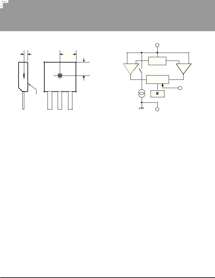
SENSOR LOCATION |
FUNCTIONAL BLOCK DIAGRAM |
|||||
(±0.005Ó [0.13 mm] die placement) |
1 |
BUS |
|
|||
ACTIVE AREA DEPTH |
|
|
|
|
||
|
|
|
|
|
|
|
0.015" |
|
|
0.090" |
|
|
|
0.38 mm |
|
|
|
|
|
|
|
|
2.29 mm |
|
|
|
|
NOM |
|
|
|
|
|
|
|
|
|
REG |
|
|
|
|
|
|
|
|
|
|
|
|
|
0.073" |
COMP |
COMP |
|
|
|
|
|
|
|
|
|
|
|
1.85 mm |
|
|
|
|
|
|
|
CLOCK |
RESET |
|
|
|
|
|
CMOS LOGIC |
|
|
A |
|
|
|
|
3 |
SWITCH IN |
|
|
|
|
(OPTIONAL) |
||
BRANDED |
1 |
2 |
3 |
|
|
|
SURFACE |
|
|
|
|||
|
|
|
|
2 |
GROUND |
Dwg. FH-009 |
|
|
|
|
|
|
|
|
|
|
Dwg. MH-002-10A |
|
|
|
DEFINITION OF TERMS
Sensor Address
Each bus sensor has a factory-specified predefined address. At present, allowable sensor addresses are integers from 01 to 30.
LOW-to-HlGH Clock Threshold (VCLH)
Minimum voltage required during the positive-going transition to increment the bus address and trigger a diagnostic response from the bus sensors. This is also the maximum threshold of the on-chip comparator that monitors the supply voltage, VBUS.
HlGH-to-LOW Threshold (VHL)
Maximum voltage required during the negative-going transition to trigger a signal current response from the bus sensors. This is also the maximum threshold of the on-chip comparator that monitors the supply voltage,
VBUS.
Bus HIGH Voltage (VH)
Bus HIGH voltage during addressing. Voltage should be greater than VCLH.
Address LOW Voltage (VL)
Bus LOW voltage during addressing. Voltage should be greater than VRST and less than VCHL.
Bus Reset Voltage (VRST)
Voltage level while resetting sensors.
Sensor Quiescent Current Drain (IQ)
The current drain of bus sensors when active but not addressed. IQH is the quiescent current drain when the sensor is not addressed and is at VH IQL is the quiescent current drain when the sensor is not addressed and is at VL. Note that IQL is greater than IQH.
Diagnostic Phase
Period on the bus when the address voltage is at VH. During this period, a correctly addressed sensor responds by increasing its current drain on the bus. This response from the sensor is called the diagnostic response and the bus current increase is called the diagnostic current.
Signal Phase
Period on the bus when the address voltage is at VL. During this period, a correctly addressed sensor that detects a magnetic field greater than the magnetic operate point, BOP, responds by maintaining a current drain of IS on the bus. This response from the sensor is called the signal response and the bus current is called the signal current.
Sensor Address Response Current (IS)
Sensor current during the diagnostic and the signal responses of the bus sensor. This is accomplished by enabling an internal constant-current source.

3054
MULTIPLEXED TWO-WIRE
HALL-EFFECT SENSOR ICs
ADDRESSING PROTOCOL
Magnetic Operate Point (BOP)
Minimum magnetic field required to switch ON the Hall amplifier and switching circuitry of the addressed sensor. This circuitry is only active when the sensor is addressed.
Magnetic Release Point (BRP)
Magnetic field required to switch OFF the Hall amplifier and switching circuitry after the output has been switched ON. When a device is deactivated by changing the bus address, all magnetic memory is lost.
Magnetic Hysteresis (BHYS)
Difference between the BOP and BRP magnetic field thresholds.
A device may be addressed by changing the supply voltage as shown in Figure 1. A preferred addressing protocol is as follows: the bus supply voltage is brought low (<2.5 V) so that all devices on the bus are reset. The voltage is then raised to the address LOW voltage (VL) and the bus quiescent current is measured. The bus is then toggled between VL and VH (address HIGH voltage), with each positive transition representing an increment in the bus address. After each voltage transition, the bus current may be monitored to check for diagnostic and signal responses from sensor ICs.
Sensor Addressing
When a sensor detects a bus address equal to its factory-programmed address, it responds with an increase in its supply current drain ( IS) during the next HIGH portion
|
|
|
FIGURE 1 |
|
|
|
|
|
|
BUS TIMING |
|
|
|
|
DIAGNOSTIC |
DIAGNOSTIC |
DIAGNOSTIC |
DIAGNOSTIC |
DIAGNOSTIC |
DIAGNOSTIC |
|
ADDRESS 01 |
ADDRESS 02 |
ADDRESS 03 |
ADDRESS 04 |
ADDRESS n |
ADDRESS 01 |
|
VH |
|
|
|
|
|
|
VCLH |
|
|
|
|
|
BUS |
VCHL |
|
|
|
|
|
VL |
|
|
|
|
|
|
VOLTAGE |
|
|
|
|
|
|
|
RESET |
|
|
|
|
RESET |
|
V RST |
|
|
|
|
|
|
0 |
t plh |
t phl |
|
|
|
|
IS |
|
SENSOR 02 — |
|
|
|
|
|
|
DIAGNOSTIC CURRENT |
|
|
|
SENSOR 02 |
|
|
|
|
|
|
CURRENT |
|
|
|
|
|
|
WITH NO |
|
|
|
|
|
|
MAGNETIC |
|
|
|
|
|
|
FIELD |
I QL |
|
|
|
|
|
|
|
|
|
|
|
|
|
I QH |
|
|
|
|
|
|
0 |
|
|
|
|
|
|
|
|
SENSOR 03 — DIAGNOSTIC |
|
|
|
|
I S |
|
AND SIGNAL CURRENTS |
|
|
|
|
|
|
|
|
|
|
SENSOR 03 |
|
|
|
|
|
|
CURRENT |
|
|
|
|
|
|
WITH |
|
|
|
|
|
|
MAGNETIC |
|
|
|
|
|
|
FIELD |
I QL |
|
|
|
|
|
|
I QH |
|
|
|
|
|
|
0 |
|
|
|
|
|
|
IS |
|
|
|
|
|
TOTAL |
|
|
|
|
|
|
BUS CURRENT |
SENSOR 01 |
|
|
|
|
SENSOR 01 |
WITH |
|
|
|
|
||
NOT PRESENT |
|
|
|
|
NOT PRESENT |
|
MAGNETIC |
|
|
|
|
|
|
FIELD AT |
n • I QL |
|
|
|
|
|
SENSOR 03 |
|
|
|
|
|
|
|
n • I QH |
|
|
|
|
|
|
0 |
|
|
|
|
|
|
|
|
|
|
|
Dwg. WH-005 |
115 Northeast Cutoff, Box 15036
Worcester, Massachusetts 01615-0036 (508) 853-5000
 Loading...