

Acer AOZ1210 datasheet
AOZ1210
EZBuck™ 2A Simple Buck Regulator
General Description
The AOZ1210 is a high efficiency, simple to use, 2A buck
regulator flexible enough to be optimized for a variety of
applications. The AOZ1210 works from a 4.5V to 27V
input voltage range, and provides up to 2A of continuous
output current on each buck regulator output. The output
voltage is adjustable down to 0.8V.
Features
●
4.5V to 27V operating input voltage range
●
70m Ω internal NFET, efficiency: up to 95%
●
Internal soft start
Output voltage adjustable down to 0.8V
●
2A continuous output current
●
Fixed 370kHz PWM operation
●
Cycle-by-cycle current limit
●
●
Short-circuit protection
●
Thermal shutdown
●
Small size SO-8 packages
Applications
●
Point of load DC/DC conversion
Set top boxes
●
DVD drives and HDD
●
LCD Monitors & TVs
●
Cable modems
●
●
Telecom/Networking/Datacom equipment
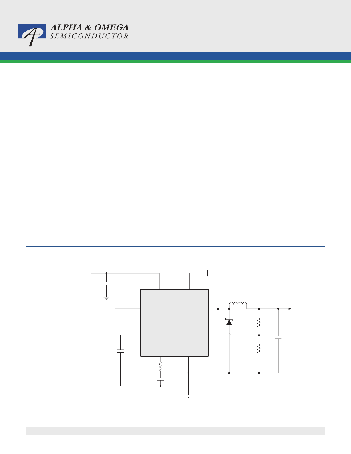
Typical Application
VIN
C1
22µF
VIN BS
EN
AOZ1210
VBIAS
C4
Figure 1. 3.3V/2A Buck Regulator
COMP
R
GND
C
C
C
LX
FB
C7
L1
6.8µH
VOUT
R1
C4, C6
22µF
R2
Rev. 1.3 December 2007
www.aosmd.com
Page 1 of 14
Ordering Information
AOZ1210
Part Number
Ambient Temperature Range Package Environmental
AOZ1210AI -40°C to +85°C SO-8 RoHS
All AOS Products are offering in packaging with Pb-free plating and compliant to RoHS standards.
Please visit www.aosmd.com/web/quality/rohs_compliant.jsp for additional information.
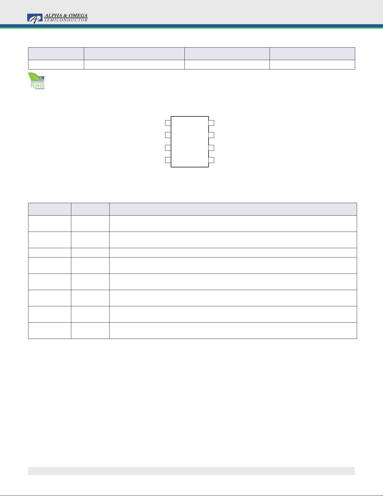
Pin Configuration
LX
BST
GND
FB
1
2
3
4
SO-8
(Top View)
8
7
6
5
VBIAS
VIN
EN
COMP
Pin Description
Pin Number
1LXPWM output connection to inductor. LX pin needs to be connected externally. Thermal connection
2 BST Bootstrap voltage input. High side driver supply. Connected to 0.1µF capacitor between BST and
3 GND Ground.
4FBFeedback input. It is regulated to 0.8V. The FB pin is used to determine the PWM output voltage
5 COMP External loop compensation. Output of internal error amplifier. Connect a series RC network to
6ENEnable pin. The enable pin is active HIGH. Connect EN pin to V
7V
8 VBIAS Compensation pin of internal linear regulator. Place put a 1µF capacitor between this pin and
Pin Name Pin Function
for output stage.
LX.
via a resistor divider between the output and GND.
GND for control loop compensation.
pin floating.
IN
Supply voltage input. Range from 4.5V to 27V. When V
device starts up. All V
pins need to be connected externally.
IN
ground.
IN
if not used. Do not leave the EN
IN
rises above the UVLO threshold the
Rev. 1.3 December 2007
www.aosmd.com
Page 2 of 14
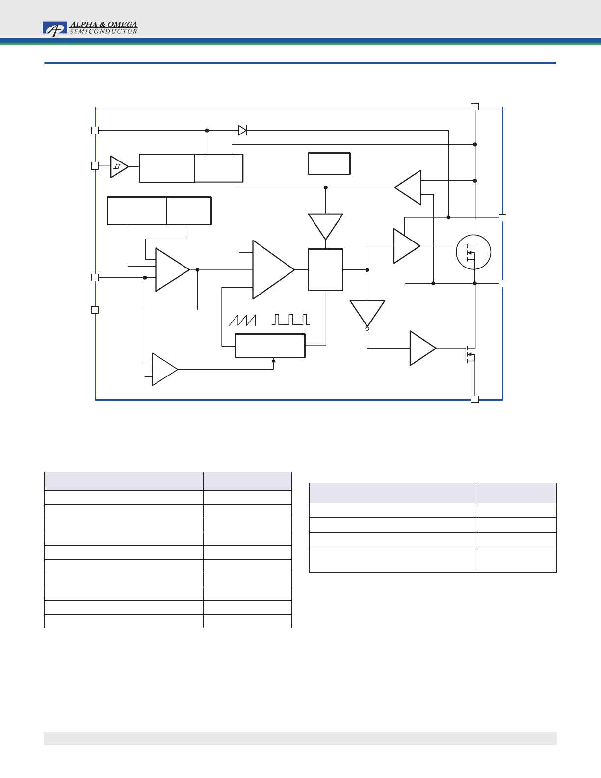
Block Diagram
AOZ1210
VIN
VBIAS
EN
FB
COMP
Reference
& Bias
0.8V
0.2V
+5V
& POR
+
–
UVLO
Softstart
GM = 200µA/V
+
EAmp
–
Frequency
Foldback
Comparator
5V LDO
Regulator
+
PWM
–
Comp
+
370kHz/24kHz
Oscillator
OTP
ILimit
PWM
Control
Logic
ISen
+
–
BST
Q1
LX
Q2
GND
Absolute Maximum Ratings
Exceeding the Absolute Maximum Ratings may damage the device.
Parameter
Supply Voltage (V
LX to GND -0.7V to V
EN to GND -0.3V to V
FB to GND -0.3V to 6V
COMP to GND -0.3V to 6V
BST to GND V
VBIAS to GND -0.3V to 6V
Junction Temperature (T
Storage Temperature (T
ESD Rating: Human Body Model
Note:
1. Devices are inherently ESD sensitive, handling precautions are
required. Human body model rating: 1.5k Ω in series with 100pF.
) 30V
IN
) +150°C
J
) -65°C to +150°C
S
(1)
Rating
+0.3V
IN
+0.3V
IN
LX
+6V
2kV
Recommend Operating Ratings
The device is not guaranteed to operate beyond the Maximum
Operating Ratings.
Parameter
Supply Voltage (V
Output Voltage Range 0.8V to V
Ambient Temperature (T
Package Thermal Resistance SO-8
)
(2
( Θ
)
JA
Note:
2. The value of
FR-4 board with 2oz. Copper, in a still air environment with T
The value in any given application depends on the user's specific
board design.
) 4.5V to 27V
IN
) -40°C to +85°C
A
Θ
is measured with the device mounted on 1-in
JA
Rating
105°C/W
A
= 25°C.
IN
2
Rev. 1.3 December 2007
www.aosmd.com
Page 3 of 14
mV
V
AOZ1210
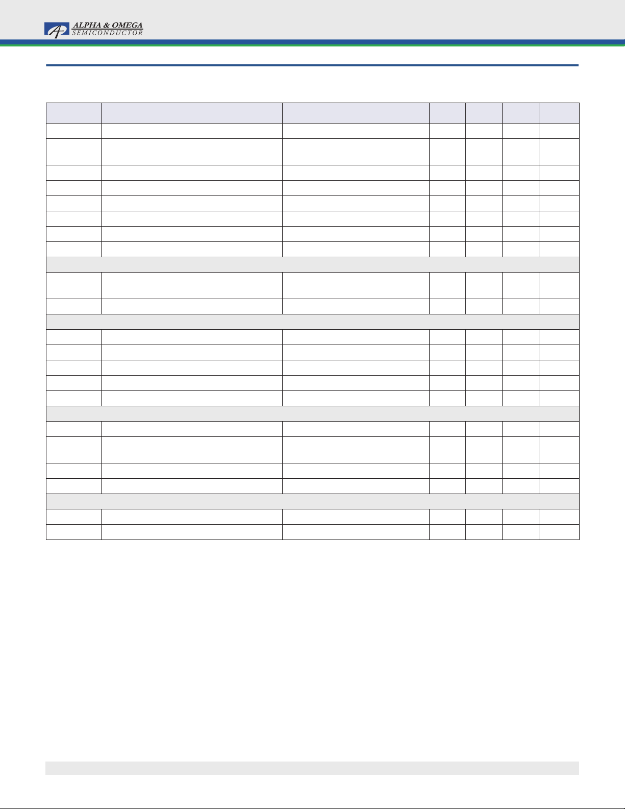
Electrical Characteristics
T
= 25°C, V
A
Symbol
V
IN
V
UVLO
I
IN
I
OFF
V
FB
= V
IN
= 12V, V
EN
= 3.3V unless otherwise specified
OUT
Parameter Conditions Min. Typ. Max. Units
Supply Voltage
Input Under-Voltage Lockout Threshold V
Supply Current (Quiescent) I
Shutdown Supply Current V
Feedback Voltage 0.782 0.8 0.818 V
V
OUT
IN
IN
EN
Rising
Falling
= 0, V
= 0V
)
(3
FB
= 1.2V, V
EN
> 2V
4.5 27
4.3
4.1
23 mA
320 µA
Load Regulation 0.5 %
Line Regulation 0.08 % / V
I
FB
Feedback Voltage Input Current 200 nA
ENABLE
V
V
HYS
EN
EN Input Threshold Off Threshold
On Threshold
EN Input Hysteresis
2.5
200
MODULATOR
D
D
G
f
MAX
VEA
G
O
MIN
EA
Frequency 315 370 425 kHz
Maximum Duty Cycle 85 %
Minimum Duty Cycle 6%
Error Amplifier Voltage Gain 500 V
Error Amplifier Transconductance 200 µA
PROTECTION
I
f
t
LIM
SC
SS
Current Limit 3.5 5.0 A
Over-Temperature Shutdown Limit T
Short Circuit Hiccup Frequency V
Rising
J
T
Falling
J
= 0V 24 kHz
FB
145
100
Soft Start Interval 4ms
PWM OUTPUT STAGE
R
DS(ON)
Note:
3. Specification in BOLD indicate an ambient temperature range of -40°C to +85°C. These specifications are guaranteed by design.
High-Side Switch On-Resistance 70 100 m Ω
High-Side Switch Leakage V
= 0V, V
EN
= 0V 10 µA
LX
0.6
V
V
V
°C
/ V
/
Rev. 1.3 December 2007
www.aosmd.com
Page 4 of 14
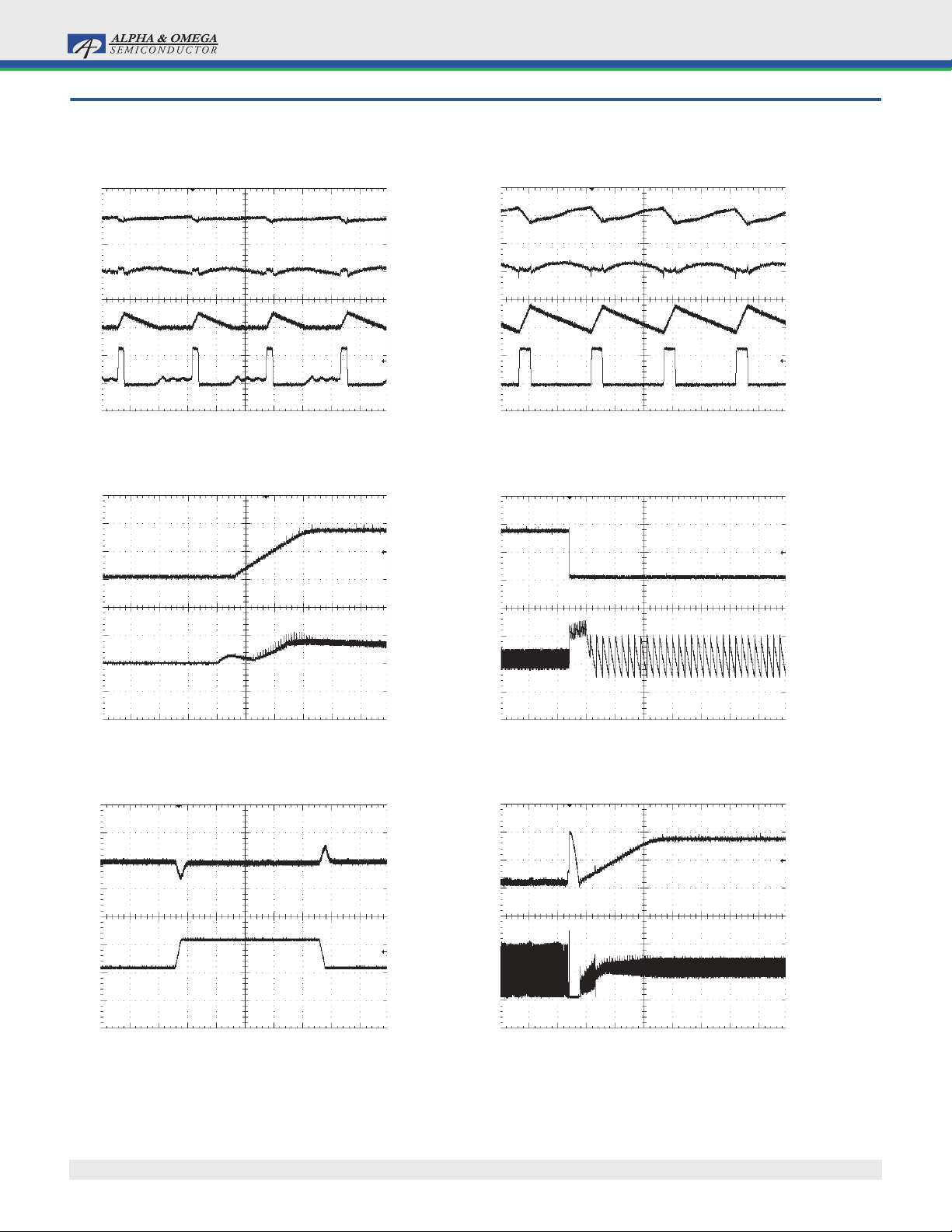
Typical Performance Characteristics
Circuit of Figure 1. T
Light Load (DCM) Operation Full Load (CCM) Operation
= 25°C, V
A
IN
= V
= 24V, V
EN
OUT
= 3.3V unless otherwise specified.
AOZ1210
Vin ripple
0.1V/div
Vo ripple
20mV/div
IL
1A/div
VLX
20V/div
1µs/div 1µs/div
Startup to Full Load Short Circuit Protection
Vo
2V/div
lin
0.5A/div
Vin ripple
0.1V/div
Vo ripple
20mV/div
IL
1A/div
VLX
20V/div
Vo
2V/div
lL
2A/div
50% to 100% Load Transient Short Circuit Recovery
Rev. 1.3 December 2007
2ms/div 200µs/div
Vo Ripple
200mV/div
lo
1A/div
200µs/div 2ms/div
www.aosmd.com
Vo
2V/div
IL
2A/div
Page 5 of 14
 Loading...