

Page 1
Data sheet
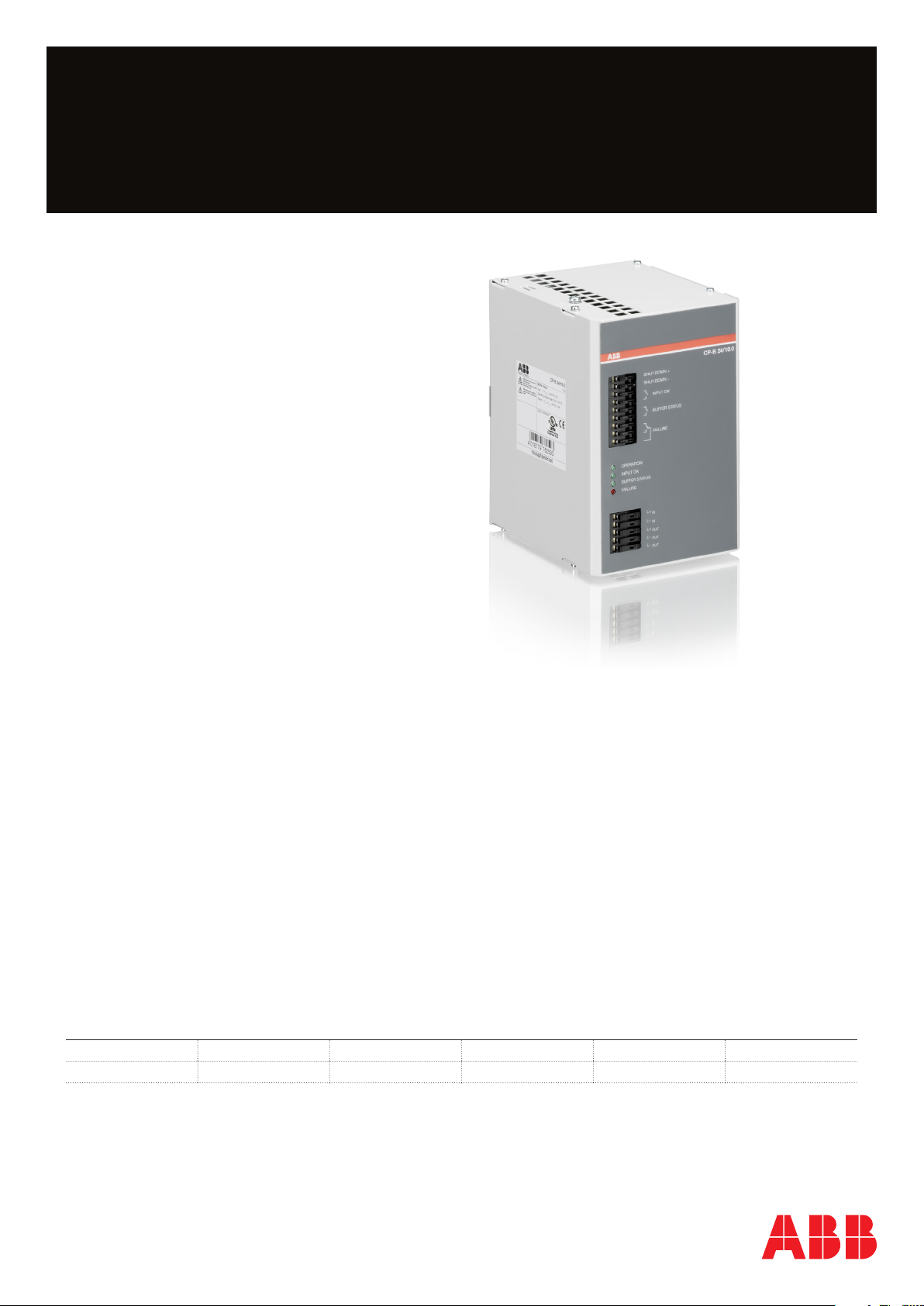
Buffer module CP-B 24/10.0, ultra-capacitor based
Accessory for power supplies
(e.g. switch mode power supplies CP range)
The CP-B 24/10.0 serves to ensure a short-
term uninterrupted power supply system with a
voltage of 24 V DC by buffering the load in case of
power loss.
The buffer module features a new technology
of storing energy by using ultra-capacitors
which entirely obviate the need for maintenance
and exempt deep discharge in comparison to
batteries.
Characteristics
– Buffer module for supporting the supply system
in case of mains failure
– Rated input voltage 24 V DC
– Rated output voltage 24 V DC
– Rated input current 10 A
– Rated output current 10 A
– Typical charging time < 134 s at 100 % load current
– Typical buffering time > 38 s at 100 % load current
– 2 relay contacts, normally open, ‘INPUT OK’ and
‘BUFFER STATUS’ status signal
– 1 relay contact, change-over, ‘FAILURE’ status signal
– 4 LEDs for indication of operational states
– 1 control signal input for specifical switch off, ‘SHUT-DOWN’
– Maintenance free
– Temperature resistant
– No deep discharge
Order data
2CDC 271 002 S0010
Buffer module
Type Rated input voltage Input voltage range Rated output voltage Rated output current Order code
CP-B 24/10.0 24 V DC 23.9-27 V DC 24 V DC 10 A 1SVR 427 060 R1000
Page 2

Functions
max. 10
nl
Operating controls and terminals
1
Signalling
SHUT-DOWN+, SHUT-DOWN-: Input signal terminals
INPUT OK, BUFFER STATUS, FAILURE:
Signalling contact – terminals
2
Indication of operational states
1
OPERATION: Buffer module in operation
(standby or buffering)
INPUT OK: Input voltage applied
BUFFER STATUS, FAILURE: details see table ‘LEDs,
status information and fault messages’ on page 4
3
Input terminals
L+IN, L-IN: Input voltage terminals
4
Output terminals
L+
OUT
, L-
OUT, L-OUT
: Output voltage terminals
2CDC 271 002 S0010
2
3
4
Application
In most areas of energy management and automation technology power supply systems have to be highly reliable. Often
batteries are used for supporting the supply system in case of mains failures. Batteries have limited lifetimes depending on
environmental parameters and, therefore, have to be maintained regularly, which causes efforts and costs.
Using the latest ultra-capacitor technology, ABB offers an innovative and completely maintenance-free new product for
buffering the 24 V DC supply at 10 A in case of interrupted mains on the primary side of the power supply.
The CP-B 24/10.0 buffer module provides an ultra-capacitor buffered energy storage for power supply units. It ensures a
short-term uninterrupted power supply system. In case of power loss, the energy stored in the capacitors guarantees that
the load is continually provided, depending on the load current, up to several hundred seconds.
Example of application
L
N
L+
L
-
IN
IN
CP-B 24/10.0
L
-
L+
OUT
OUT
A
buffered
L+
-
L
load 1load
...
2 - Buffer module CP-B 24/10.0, ultra-capacitor based | Data sheet
max. 20 A
CP-C 24/20.0
L+
-
L
unbuffered
L+
-
L
...
oad 1load n
2CDC 273 009 F0210
Page 3
Operating mode
60
70
Temperature [°C]
Years
A power supply has to be connected to the buffer module‘s terminals L+IN and L-IN. Once the input voltage has been
applied, the buffer module starts loading its ultra-capacitors. Having achieved an energy level greater than 80 % of the
nominal capacitance, the LED ‘BUFFER STATUS’ glows. Regardless of the energy level, the buffer module provides the
according output voltage after having applied the minimum charging potential on the input side for about 2 s.
In case of interrupted mains on the primary side of the power supply the buffer module guarantees that the load connected
to terminals L+
OUT
and L-
is continually provided. In order to display the interrupted supply on the primary side the LED
OUT
‘INPUT OK‘ turns off while the capacitors are being discharged. When the energy level drops below 30 % of the nominal
capacitance, the LED ‘BUFFER STATUS’ turns off.
The LED ‘FAILURE’ indicates faults due to overvoltage at the internal capacitors as well as overcurrent at the output.
The messaging relays ‘INPUT OK’, ‘BUFFER OK’ and ‘FAILURE’ are coupled with the correspondent LED which glows
while the according relay is energized.
Important operating features
To trigger a safe shut-down of connected loads, a 24 V DC control signal can be applied to the terminals labelled
‘SHUT-DOWN+’ and ‘SHUT-DOWN-’. This effects that buffered loads can be switched off in a defined state. Furthermore
the shut-down can be used if a specific energy level of the capacitors has to be conserved.
Its advantage is that a subsequent charging of the capacitors can be shortened.
Decommissioning
To put the buffer module out of operation, the power supply has to be turned off. Subsequently the buffer module continues
to supply the load until the capacitors are discharged.
In order to circumvent the subsequent buffering operation and the discharge of the capacitors, the module can be directly
switched off by activating the shut-down without buffering. All LEDs turn off immediately.
Functional interaction of power supply and buffer module in charging operation
The buffer module’s ultra-capacitors require a minimum charging potential, which has to be provided by the power supply.
The minimum charging potential is necessary to charge the capacitors or to preserve the energy level in case of fully loaded
capacitors. The charging process and the charging time of the buffer module depend on the input and the load current.
Having buffered and unbuffered loads connected to the power supply result in a split up of its provided current into parallel
divided circuits (see ’Example of application’ on page 2).
In order to use the maximum available current provided by the power supply, the buffer module acts as a variable load.
The module decreases its load, if the rated input current of the buffer module would cause the power supply to cut the
output voltage down (load limiting function) or to perform a slow lowering of the output voltage, resulting in an input voltage
lower than the specified minimum charging potential. In this way the buffer module ascertains the fastest possible charging
process according to the power supply used.
Note: It is highly recommended that loads which do not need an uninterrupted supply are connected directly, in parallel
to all buffered loads, with the power supply. Buffering such loads would only reduce the buffering time which is load
dependent. Therefore loads should be selected as small as necessary in order to achieve high buffering times.
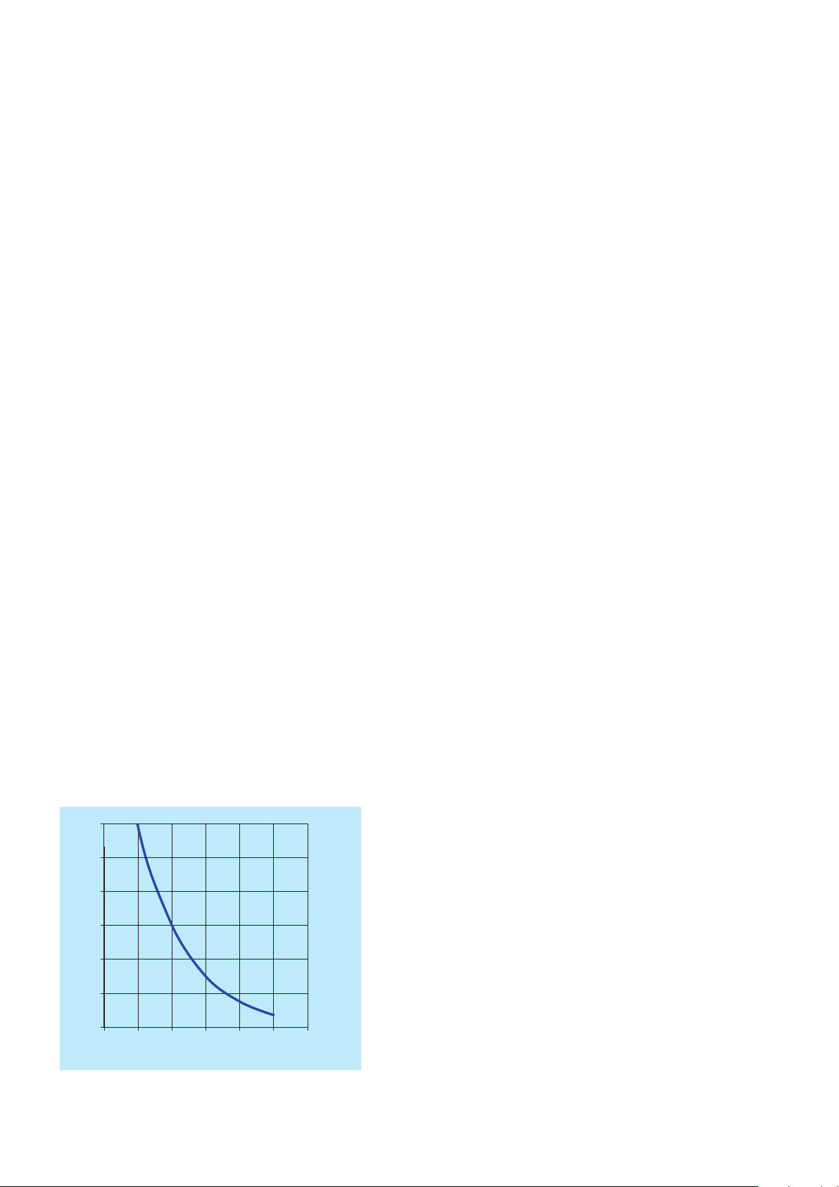
Note: The capacitor’s life span depends on the temperature
exposed to as shown in the figure below as well as on the load
50
40
current. The end of the life span is reached, when its capacitance
drops below 70 % of its nominal capacitance. Using
the buffer
module continuously at its specified maximum applicable
temperature, the expected product lifetime is approximately 5 years.
30
20
10
0
Capacitor’s life span over temperature
302010
40 50
60
2CDC 272 031 F0210
Data sheet | Buffer module CP-B 24/10.0, ultra-capacitor based - 3
Page 4

Indication of operational states
(A)
115.6
(B)
LEDs, status information and fault messages
Operating state INPUT OK
LED green
Input voltage applied
Device in operation (input voltage applied or internally supplied
V V
--
OPERATION
LED green
V
BUFFER STATUS
LED green
-- --
-- --
FAILURE
LED red
by using energy stored in capacitors)
Charging process
Energy stored in capacitors > 80 % (while charging)
Energy stored in capacitors < 30 % (while discharging) OFF
Capacitors discharged (load no longer supplied, only internal
(energy stored in capacitors > 30 and < 80 % )
V V
-- --
V V V
OFF
--
OFF
V
V
--
V
V
supply is maintained)
Overvoltage at internal capacitors, overcurrent at output,
--
V
--
V
overvoltage at input terminal
Capacitors discharged or shut-down activated OFF OFF OFF OFF
-- = not relevant
Installation
The device must be installed by qualified persons only and in accordance with the specific national regulations (e.g. VDE,
etc.). The CP-B 24/10.0 is a chassis-mounted unit. It is maintance-free and does not contain any integral setting elements
and should therefore not be opened.
If the buffer module is built into systems needing overvoltages for testing (e.g. EN 60204-1/ VDE0113 part1 19.4 voltage
control), the module must be disconnected during the test. (Original text EN 60204-1: components, which are not
dimensioned for the testing voltage must be separated during the testing.)
Note: The device is completely maintenance free. The enclosure is sealed.
DANGER!
Components with high stored energy
Danger to be electrocuted!
► Disconnect the system from the supply network and protect against switching on before any installation,
maintenance or modification work.
► Discharge the buffer module completely.
► Do not introduce any objects into the unit and do not open the unit.
► Ensure that the service personnel is protected against inadvertent contact with parts carrying energy.
Mounting position
4.55"
The device has to be mounted horizontally with the input terminals
on the bottom. In order to ensure a sufficient convection, the
minimum distance to the other modules must be not less than
(B)
40 mm (1.58 in) in vertical direction. Minimum distance in horizontal
direction is not necessary.
SHUT-DOWN +
SHUT-DOWN -
INPUT OK
BUFFER STATUS
OPERATION
INPUT OK
BUFFER STATUS
FAILURE
FAILURE
L+
IN
L-
IN
L+
OUT
L-
OUT
L-
OUT
CP-B 24/10.0
(A)
6.42"
163
5.43"
137.8
4 - Buffer module CP-B 24/10.0, ultra-capacitor based | Data sheet
2CDC 272 025 F0010
Page 5

Electrical connection
The installation must be executed according to EN 60950 and possible applicable local standards. The input side is
protected by an internal input fuse.
L+IN L-IN Input voltage
IN
L+
L
-
SHUT
DOWN+
SHUT
DOWN
-
Connection diagram
OUT
L+
L
-
L
-
INPUT
OK
BUFFER
STATUS
FAILURE
SHUT-DOWN+
SHUT-DOWN
INPUT OK
INPUT OK
BUFFER STATUS
BUFFER STATUS
FAILURE
FAILURE
FAILURE
L+
L
L+
L
-
L
-
-
IN
-
IN
OUT
OUT
OUT
L+
L-
L-
OUT
OUT
Output voltage
OUT
INPUT OK Signalling contact (relay)
BUFFER STATUS Signalling contact (relay)
FAILURE Signalling contact (relay)
SHUT-DOWN Input control signal
2CDC 272 021 F0010
1. Connect the load to be buffered to the output terminals L+
OUT
and L-
OUT
.
2. The signalling contact ‘INPUT OK’ can be used for external status analysis.
In case of overload, the output current comprises the maximum current of the buffer module as well as the current of the
power supply unit. The overload protection has to be realized externally.
Rate the lines for the maximum output current or provide separate fuse protection. It is recommended to choose the wire
size as large as possible in order to minimize voltage drops. Observe the polarity. The device is overload and open-circuit
proof.
Operation
DANGER!
High current
Risk of electric arcs and electric shocks!
► Do not modify the installation (primary and secondary side).
► Intended use.
CAUTION!
Enclosure can become very hot depending on the operation conditions
Risk of burns!
► In order to ensure sufficient air-cooling the distance to other devices has to be considered.
Before start of operation the following must be ensured:
1. Connect electrical lines according to the specific national regulations for class of protection III.
2. Power supply cables and unit must be sufficiently fused.
3. A disconnection device has to be provided for the power supply to disengage unit and supply cables from supply
mains if required.
4. Rate the output lines for the output current of the buffer module and connect them with the correct polarity.
If the buffer module is entirely charged and works in the standby mode, there is no heating of the module. From the thermal
point of view this can be compared with a switched-off device.
The device is intended for use as a buffer module. Any other usage is not supported by the manufacturer. Other usage,
improper installation or operation may impair safety and cause operational difficulties or destruction of the unit.
Service
The internal fuse is not user-replaceable. If the internal fuse blows, most probably the device is defective. In this case, an
examination of the buffer module by the manufacturer is necessary.
Data sheet | Buffer module CP-B 24/10.0, ultra-capacitor based - 5
Page 6

Technical data
Data at Ta = 25 °C and rated values, unless otherwise indicated
Input circuits
Supply circuit L+IN L-
Rated input voltage U
in
IN
24 V DC
Input voltage range 23.9-27 V DC
Minimum charging potential 23.9 V DC
Rated input current 10 A DC
Inrush current limiting 35 A / 2 ms
Transient overvoltage protection varistor / suppressor diode
Internal input fuse (apparatus protection, not accessible) 15 A (FK2)
Internal fuse capacitors circuit (not accessible) 25 A (FK2)
Kind of input SHUT-DOWN control input
rated voltage 24 V DC
voltage range 6-45 V DC
Indication of operational states
details see table ‘LEDs, status information and fault
messages’ on page 4
Input voltage INPUT OK LED green
Internal system voltage OPERATION LED green
Energy storage level BUFFER STATUS LED green
Fault status FAILURE LED red
Output circuits
L+
L-
OUT
L-
OUT
r
OUT
Rated output power 240 W
Rated output voltage U
out
24 V DC
Output voltage (buffer mode) 23.2 V DC
Tolerance of the output voltage +2...-10 %
Rated output current I
r
Ta ≤ 60 °C 10 A DC
Peak output current (fully loaded capacitors required) Ta ≤ 60 °C 20 A DC (10 A power supply + 10 A CP-B, min. 1.5 s)
Control of limiting current 10.3 A DC ±0.1 A
Shut-down if limiting current is exceeded after 1.5 s
Short-circuit protection (via internal 15 A fuse and external 10 A fuse) no continuous short-circuit stability
Internal output fuse (not accessible) 15 A (FK2)
Required external fuse 10 A slow acting
Current limiting at output circuit 1.05...1.2 x I
Breaking capacity of output circuit
τ = 2,5 ms
24 V DC, 10 A
Power failure buffering time load-dependent, min. 38 s at 100 % load
Overload protection thermal protection
Kind of output INPUT OK n/o contact
BUFFER STATUS n/o contact
FAILURE c/o contact
Contact material Ag + Au-clad
Minimum switching voltage / Minimum switching current 5 V DC / 1 mA
Maximum switching voltage / Maximum switching current 50 V AC / 1 A, 30 V DC / 0.5 A
Mechanical lifetime 5 x 10⁶ switching cycles
Electrical lifetime 0.1 x 10⁶ switching cycles
Maximum fuse rating to achieve short-circuit protection n/o or n/c contact 1.0 A AC / 0.5 A DC
6 - Buffer module CP-B 24/10.0, ultra-capacitor based | Data sheet
Page 7

General data
MTBF available on request
Maximum internal power consumption 20 W
Power consumption with unloaded output 3 W
Energy storage (min.) 10000 Ws
Typical charging time at load current 100 % 134 s
0 % 82 s
Typical buffering time at load current
Efficiency greater than 90 %
Duty time 100 %
Dimensions see "Dimensional drawings"
Weight net 2.1 kg (4.63 lb)
Material of enclosure cover steel sheet powdered
Mounting
Mounting position horizontal
Minimum distance to other units horizontal not necessary
Pollution degree 2
Degree of protection enclosure IP20
Protection class (IEC/EN 61140) III SELV / PELV (condition: power supply fulfills class III)
1)
buffering time ≈
energy storage x 0.9
load current x 23.2 V
1)
100 % 38 s
50 % 76 s
25 % 140 s
10 % 380 s
enclosure shell steel sheet powdered
DIN rail (IEC/EN 60715), snap-on mounting
vertical 40 mm (1.58 in)
terminal IP20
Electrical connection (pull spring terminals)
Input circuit, output circuit
Connecting capacity fine-strand with(out) wire end ferrule 0.08-1.5 mm² (28-18 AWG)
rigid 0.08-4.0 mm² (28-16 AWG)
Stripping length 6.0 mm (0.24 in)
Signalling circuit
Connecting capacity fine-strand with(out) wire end ferrule 0.08-1.0 mm² (28-18 AWG)
rigid 0.08-1.5 mm² (28-16 AWG)
Stripping length 6.0 mm (0.24 in)
Environmental data
Ambient temperature operation -40...+60 °C (-40...+140 °F)
storage -40...+60 °C (-40...+140 °F)
Vibration, sinusoidal based on IEC/EN 60068-2-6 1.5 mm, 3-57.55 Hz; 2 g, 57.55-500 Hz, 10 cycles
Shock, half-sine based on IEC/EN 60068-2-27 15 g, 11 ms, 3 axes, 6 faces, 3 times for each face
Data sheet | Buffer module CP-B 24/10.0, ultra-capacitor based - 7
Page 8

Standards / Directives
I
[A]
Normal application (up to
ging
10.0
Standards
Low Voltage Directive
EMC Directive
RoHS Directive
EN 50178, IEC/EN 60950-1, IEC/EN 62040-2
2014/35/EU
2014/30/EU
2011/65/EU
Electromagnetic compatibility
Interference immunity to IEC/EN 61000-6-2
electrostatic discharge IEC/EN 61000-4-2 Level 3, 6 kV / 8 kV
radiated, radio-frequency, electromagnetic field IEC/EN 61000-4-3 Level 3, 10 V/m (27-1000 MHz) /
Level 2, 3 V/m (1400-2700 MHz)
electrical fast transient / burst IEC/EN 61000-4-4 Level 3, 2(1) kV / 5 kHz
surge IEC/EN 61000-4-5 Level 1, 0.5 kV
conducted disturbances, induced by radio-frequency fields IEC/EN 61000-4-6 Level 3, 10 V (150 kHz-80 MHz)
voltage dips, short interruptions and voltage variations IEC/EN 61000-4-11 buffered by ultra-capacitors
Interference emission EN 61000-6-4
high-frequency radiated DIN EN 55011 B/C1
high-frequency conducted DIN EN 55011 B/C1
Technical diagrams
Temperature behavior
out
7.5
5.0
-40
Characteristic curve of the temperature at rated load
0204060
-20
50 % buffer mode, 5 char
and discharging cycles in
direct series)
Continuous charging and
discharging in direct series.
As this is not typical of a real
application, this should
be considered as theoretical
indication
Ta [°C]
2CDC 272 029 F0210
8 - Buffer module CP-B 24/10.0, ultra-capacitor based | Data sheet
Page 9

Dimensions
in mm and inches
IEC/EN 60715
TH 35-7.5
TH 35-15
163.0 6.42"
167.9 6.61"
CP-B 24/10.0
137.8 5.43"
145.3 5.72"
151.0 5.95"
115.6 4.55"
2CDC 272 008 F0017
Data sheet | Buffer module CP-B 24/10.0, ultra-capacitor based - 9
 Loading...