

Page 1
ABB industrial drives
Firmware manual
ACS880 IGBT supply control program
Page 2

List of related manuals
General manuals Code (English)
Safety instructions for ACS880 multidrive cabinets and modules 3AUA0000102301
Electrical planning instructions for ACS880 multidrive cabinets
and modules
Mechanical installation instructions for ACS880 multidrive
cabinets
Cabinet design and construction instructions for ACS880 air-
cooled and liquid-cooled multidrive modules
Inverter module manuals and guides
ACS880-104 inverter modules hardware manual 3AUA0000104271
ACS880-104LC inverter modules hardware manual 3AXD50000045610
ACS880 primary control program firmware manual 3AUA0000085967
ACS880 primary control program quick start-up guide 3AUA0000098062
Supply module manuals
ACS880-204 IGBT supply modules hardware manual 3AUA0000131525
ACS880 IGBT supply control program firmware manual 3AUA0000131562
ACS880-304 +A003 diode supply modules hardware manual 3AUA0000102452
ACS880-304 +A018 diode supply modules hardware manual 3AXD50000010104
ACS880-304LC+A019 diode supply modules hardware manual 3AXD50000045157
ACS880 diode supply control program firmware manual 3AUA0000103295
ACS880-904 regenerative rectifier modules hardware manual 3AXD50000020457
ACS880 regenerative rectifier control program firmware manual 3AXD50000020827
3AUA0000102324
3AUA0000101764
3AUA0000107668
Brake module and DC/DC converter module manuals
ACS880-604 1-phase brake chopper units as modules hardware
manual
ACS880-604 3-phase brake modules hardware manual 3AXD50000022033
ACS880 brake control program firmware manual 3AXD50000020967
ACS880-1604 DC/DC converter modules hardware manual 3AXD50000023642
ACS880 DC/DC converter control program firmware manual 3AXD50000024671
Cabinet-installed multidrive manuals
ACS880-107 inverter units hardware manual 3AUA0000102519
ACS880-207 IGBT supply units hardware manual 3AUA0000130644
ACS880-307 (+A003) diode supply units hardware manual 3AUA0000102453
ACS880-307 +A018 diode supply units hardware manual 3AXD50000011408
ACS880-607 1-phase brake units hardware manual 3AUA0000102559
ACS880-607 3-phase brake units hardware manual 3AXD50000022034
ACS880-907 regenerative rectifier units hardware manual 3AXD50000020546
ACS880-1607 DC/DC converter units hardware manual 3AXD50000023644
Option manuals and guides
ACX-AP-x assistant control panels user’s manual 3AUA0000085685
Drive composer start-up and maintenance PC tool user’s manual 3AUA0000094606
Manuals and quick guides for I/O extension modules, fieldbus
adapters, safety options, application programs etc.
3AUA0000106244
You can find manuals and other product documents in PDF format on the Internet. See section
Document library on the Internet on the inside of the back cover. For manuals not available in the
Document library, contact your local ABB representative.
Page 3

Firmware manual
ACS880 IGBT supply control program
Table of contents
2. Start-up
2017 ABB Oy. All Rights Reserved.
3AUA0000131562 Rev F
EN
EFFECTIVE: 2017-08-30
Page 4

Page 5

5
Table of contents
1. Introduction to the manual
What this chapter contains . . . . . . . . . . . . . . . . . . . . . . . . . . . . . . . . . . . . . . . . . . . . . . . . 9
Applicability . . . . . . . . . . . . . . . . . . . . . . . . . . . . . . . . . . . . . . . . . . . . . . . . . . . . . . . . . . . . 9
Safety instructions . . . . . . . . . . . . . . . . . . . . . . . . . . . . . . . . . . . . . . . . . . . . . . . . . . . . . . . 9
Target audience . . . . . . . . . . . . . . . . . . . . . . . . . . . . . . . . . . . . . . . . . . . . . . . . . . . . . . . . 9
Contents of the manual . . . . . . . . . . . . . . . . . . . . . . . . . . . . . . . . . . . . . . . . . . . . . . . . . . 10
Related documents . . . . . . . . . . . . . . . . . . . . . . . . . . . . . . . . . . . . . . . . . . . . . . . . . . . . . 10
Terms and abbreviations . . . . . . . . . . . . . . . . . . . . . . . . . . . . . . . . . . . . . . . . . . . . . . . . . 11
Cybersecurity disclaimer . . . . . . . . . . . . . . . . . . . . . . . . . . . . . . . . . . . . . . . . . . . . . . . . . 12
2. Start-up
3. Using the control panel
4. Control locations and operating modes
What this chapter contains . . . . . . . . . . . . . . . . . . . . . . . . . . . . . . . . . . . . . . . . . . . . . . . 17
Local control vs. external control . . . . . . . . . . . . . . . . . . . . . . . . . . . . . . . . . . . . . . . . . . . 18
External control . . . . . . . . . . . . . . . . . . . . . . . . . . . . . . . . . . . . . . . . . . . . . . . . . . . . . . 18
Local control . . . . . . . . . . . . . . . . . . . . . . . . . . . . . . . . . . . . . . . . . . . . . . . . . . . . . . . . 18
Operating modes . . . . . . . . . . . . . . . . . . . . . . . . . . . . . . . . . . . . . . . . . . . . . . . . . . . . . . . 19
5. Program features
What this chapter contains . . . . . . . . . . . . . . . . . . . . . . . . . . . . . . . . . . . . . . . . . . . . . . . 21
Overview of the control program . . . . . . . . . . . . . . . . . . . . . . . . . . . . . . . . . . . . . . . . . . . 21
Control program configuration and programming . . . . . . . . . . . . . . . . . . . . . . . . . . . . . . 22
Application programming . . . . . . . . . . . . . . . . . . . . . . . . . . . . . . . . . . . . . . . . . . . . . . 22
Programming via parameters . . . . . . . . . . . . . . . . . . . . . . . . . . . . . . . . . . . . . . . . . . . 22
Run enable, Start/stop and Start enable control . . . . . . . . . . . . . . . . . . . . . . . . . . . . . . . 23
Settings and diagnostics . . . . . . . . . . . . . . . . . . . . . . . . . . . . . . . . . . . . . . . . . . . . . . . 23
Control interfaces . . . . . . . . . . . . . . . . . . . . . . . . . . . . . . . . . . . . . . . . . . . . . . . . . . . . . . 24
Programmable analog inputs . . . . . . . . . . . . . . . . . . . . . . . . . . . . . . . . . . . . . . . . . . . 24
Programmable analog outputs . . . . . . . . . . . . . . . . . . . . . . . . . . . . . . . . . . . . . . . . . . 24
Programmable digital inputs and outputs . . . . . . . . . . . . . . . . . . . . . . . . . . . . . . . . . . 24
Programmable relay outputs . . . . . . . . . . . . . . . . . . . . . . . . . . . . . . . . . . . . . . . . . . . 24
Programmable I/O extensions . . . . . . . . . . . . . . . . . . . . . . . . . . . . . . . . . . . . . . . . . . 25
Fieldbus control . . . . . . . . . . . . . . . . . . . . . . . . . . . . . . . . . . . . . . . . . . . . . . . . . . . . . 25
External controller interface . . . . . . . . . . . . . . . . . . . . . . . . . . . . . . . . . . . . . . . . . . . . 26
Reference chains . . . . . . . . . . . . . . . . . . . . . . . . . . . . . . . . . . . . . . . . . . . . . . . . . . . . . . 28
DC voltage control . . . . . . . . . . . . . . . . . . . . . . . . . . . . . . . . . . . . . . . . . . . . . . . . . . . 28
Active power control . . . . . . . . . . . . . . . . . . . . . . . . . . . . . . . . . . . . . . . . . . . . . . . . . . 28
Reactive power control . . . . . . . . . . . . . . . . . . . . . . . . . . . . . . . . . . . . . . . . . . . . . . . . 29
Net lost detection . . . . . . . . . . . . . . . . . . . . . . . . . . . . . . . . . . . . . . . . . . . . . . . . . . . . . . 30
Settings and diagnostics . . . . . . . . . . . . . . . . . . . . . . . . . . . . . . . . . . . . . . . . . . . . . . . 30
Reduced run function . . . . . . . . . . . . . . . . . . . . . . . . . . . . . . . . . . . . . . . . . . . . . . . . . . . 30
Activation of the reduced run function . . . . . . . . . . . . . . . . . . . . . . . . . . . . . . . . . . . . 31
Page 6

6
Settings and diagnostics . . . . . . . . . . . . . . . . . . . . . . . . . . . . . . . . . . . . . . . . . . . . . . 31
Programmable protection functions . . . . . . . . . . . . . . . . . . . . . . . . . . . . . . . . . . . . . . . . 32
Emergency stop . . . . . . . . . . . . . . . . . . . . . . . . . . . . . . . . . . . . . . . . . . . . . . . . . . . . 32
External events . . . . . . . . . . . . . . . . . . . . . . . . . . . . . . . . . . . . . . . . . . . . . . . . . . . . . 32
Earth fault detection . . . . . . . . . . . . . . . . . . . . . . . . . . . . . . . . . . . . . . . . . . . . . . . . . 32
External earth leakage fault source selection . . . . . . . . . . . . . . . . . . . . . . . . . . . . . . 33
External earth leakage action selection . . . . . . . . . . . . . . . . . . . . . . . . . . . . . . . . . . 33
Supply phase loss detection . . . . . . . . . . . . . . . . . . . . . . . . . . . . . . . . . . . . . . . . . . . 33
Local control loss detection . . . . . . . . . . . . . . . . . . . . . . . . . . . . . . . . . . . . . . . . . . . . 33
Automatic fault resets . . . . . . . . . . . . . . . . . . . . . . . . . . . . . . . . . . . . . . . . . . . . . . . . 33
Thermal switch monitoring . . . . . . . . . . . . . . . . . . . . . . . . . . . . . . . . . . . . . . . . . . . . 34
Power limiting due to heat rise in the supply module . . . . . . . . . . . . . . . . . . . . . . . . 34
Counting the number of charging attempts . . . . . . . . . . . . . . . . . . . . . . . . . . . . . . . . 34
DC overvoltage and undervoltage protections . . . . . . . . . . . . . . . . . . . . . . . . . . . . . 35
Diagnostics . . . . . . . . . . . . . . . . . . . . . . . . . . . . . . . . . . . . . . . . . . . . . . . . . . . . . . . . . . 36
Maintenance timers and counters . . . . . . . . . . . . . . . . . . . . . . . . . . . . . . . . . . . . . . . 36
Load analyzer . . . . . . . . . . . . . . . . . . . . . . . . . . . . . . . . . . . . . . . . . . . . . . . . . . . . . . 36
User parameter sets . . . . . . . . . . . . . . . . . . . . . . . . . . . . . . . . . . . . . . . . . . . . . . . . . . . 37
Settings and diagnostics . . . . . . . . . . . . . . . . . . . . . . . . . . . . . . . . . . . . . . . . . . . . . . 37
User lock . . . . . . . . . . . . . . . . . . . . . . . . . . . . . . . . . . . . . . . . . . . . . . . . . . . . . . . . . . . . 37
Settings . . . . . . . . . . . . . . . . . . . . . . . . . . . . . . . . . . . . . . . . . . . . . . . . . . . . . . . . . . . 37
Data storage parameters . . . . . . . . . . . . . . . . . . . . . . . . . . . . . . . . . . . . . . . . . . . . . . . . 38
Settings and diagnostics . . . . . . . . . . . . . . . . . . . . . . . . . . . . . . . . . . . . . . . . . . . . . . 38
Charging . . . . . . . . . . . . . . . . . . . . . . . . . . . . . . . . . . . . . . . . . . . . . . . . . . . . . . . . . . . . 39
Timing diagram . . . . . . . . . . . . . . . . . . . . . . . . . . . . . . . . . . . . . . . . . . . . . . . . . . . . . 40
Settings and diagnostics . . . . . . . . . . . . . . . . . . . . . . . . . . . . . . . . . . . . . . . . . . . . . . 40
DDCS communication with inverter unit . . . . . . . . . . . . . . . . . . . . . . . . . . . . . . . . . . . . 41
Settings and diagnostics . . . . . . . . . . . . . . . . . . . . . . . . . . . . . . . . . . . . . . . . . . . . . . 41
Default I/O connection diagram (BCU) . . . . . . . . . . . . . . . . . . . . . . . . . . . . . . . . . . . . . 42
Default I/O connection diagram (ZCU) . . . . . . . . . . . . . . . . . . . . . . . . . . . . . . . . . . . . . 44
Parameters that define the use of relay outputs . . . . . . . . . . . . . . . . . . . . . . . . . . . . 45
Parameters that define the use of digital inputs . . . . . . . . . . . . . . . . . . . . . . . . . . . . 45
Power share with droop control . . . . . . . . . . . . . . . . . . . . . . . . . . . . . . . . . . . . . . . . . . . 47
Master/follower link . . . . . . . . . . . . . . . . . . . . . . . . . . . . . . . . . . . . . . . . . . . . . . . . . . 48
Before start . . . . . . . . . . . . . . . . . . . . . . . . . . . . . . . . . . . . . . . . . . . . . . . . . . . . . . . . 48
Settings . . . . . . . . . . . . . . . . . . . . . . . . . . . . . . . . . . . . . . . . . . . . . . . . . . . . . . . . . . . 48
Master/follower functionality . . . . . . . . . . . . . . . . . . . . . . . . . . . . . . . . . . . . . . . . . . . . . 49
General . . . . . . . . . . . . . . . . . . . . . . . . . . . . . . . . . . . . . . . . . . . . . . . . . . . . . . . . . . . 49
Communication . . . . . . . . . . . . . . . . . . . . . . . . . . . . . . . . . . . . . . . . . . . . . . . . . . . . . 49
Construction of the master/follower link . . . . . . . . . . . . . . . . . . . . . . . . . . . . . . . . . . 50
Example parameter settings . . . . . . . . . . . . . . . . . . . . . . . . . . . . . . . . . . . . . . . . . . . 52
Specifications of the fiber optic master/follower link . . . . . . . . . . . . . . . . . . . . . . . . . 53
Settings and diagnostics . . . . . . . . . . . . . . . . . . . . . . . . . . . . . . . . . . . . . . . . . . . . . . 53
6. Parameters
What this chapter contains . . . . . . . . . . . . . . . . . . . . . . . . . . . . . . . . . . . . . . . . . . . . . . 55
Terms and abbreviations . . . . . . . . . . . . . . . . . . . . . . . . . . . . . . . . . . . . . . . . . . . . . . . . 55
Reserved digital inputs and relay outputs . . . . . . . . . . . . . . . . . . . . . . . . . . . . . . . . . . . 56
Summary of parameter groups . . . . . . . . . . . . . . . . . . . . . . . . . . . . . . . . . . . . . . . . . . . 57
Parameter listing . . . . . . . . . . . . . . . . . . . . . . . . . . . . . . . . . . . . . . . . . . . . . . . . . . . . . . 58
101 Actual values . . . . . . . . . . . . . . . . . . . . . . . . . . . . . . . . . . . . . . . . . . . . . . . . . . . 58
103 Input references . . . . . . . . . . . . . . . . . . . . . . . . . . . . . . . . . . . . . . . . . . . . . . . . . 60
104 Warnings and faults . . . . . . . . . . . . . . . . . . . . . . . . . . . . . . . . . . . . . . . . . . . . . . 61
Page 7

7
105 Diagnostics . . . . . . . . . . . . . . . . . . . . . . . . . . . . . . . . . . . . . . . . . . . . . . . . . . . . . 66
106 Control and status words . . . . . . . . . . . . . . . . . . . . . . . . . . . . . . . . . . . . . . . . . . . 67
107 System info . . . . . . . . . . . . . . . . . . . . . . . . . . . . . . . . . . . . . . . . . . . . . . . . . . . . . 73
110 Standard DI, RO . . . . . . . . . . . . . . . . . . . . . . . . . . . . . . . . . . . . . . . . . . . . . . . . . 74
111 Standard DIO, FI, FO . . . . . . . . . . . . . . . . . . . . . . . . . . . . . . . . . . . . . . . . . . . . . . 78
112 Standard AI . . . . . . . . . . . . . . . . . . . . . . . . . . . . . . . . . . . . . . . . . . . . . . . . . . . . . 80
113 Standard AO . . . . . . . . . . . . . . . . . . . . . . . . . . . . . . . . . . . . . . . . . . . . . . . . . . . . 83
114 Extension I/O module 1 . . . . . . . . . . . . . . . . . . . . . . . . . . . . . . . . . . . . . . . . . . . . 86
115 Extension I/O module 2 . . . . . . . . . . . . . . . . . . . . . . . . . . . . . . . . . . . . . . . . . . . 101
116 Extension I/O module 3 . . . . . . . . . . . . . . . . . . . . . . . . . . . . . . . . . . . . . . . . . . . 105
119 Operation mode . . . . . . . . . . . . . . . . . . . . . . . . . . . . . . . . . . . . . . . . . . . . . . . . . 108
120 Start/stop . . . . . . . . . . . . . . . . . . . . . . . . . . . . . . . . . . . . . . . . . . . . . . . . . . . . . . 109
121 Start/stop mode . . . . . . . . . . . . . . . . . . . . . . . . . . . . . . . . . . . . . . . . . . . . . . . . . 114
122 Power reference . . . . . . . . . . . . . . . . . . . . . . . . . . . . . . . . . . . . . . . . . . . . . . . . 114
123 DC voltage reference . . . . . . . . . . . . . . . . . . . . . . . . . . . . . . . . . . . . . . . . . . . . . 116
124 Reactive power reference . . . . . . . . . . . . . . . . . . . . . . . . . . . . . . . . . . . . . . . . . 117
130 Limits . . . . . . . . . . . . . . . . . . . . . . . . . . . . . . . . . . . . . . . . . . . . . . . . . . . . . . . . . 121
131 Fault functions . . . . . . . . . . . . . . . . . . . . . . . . . . . . . . . . . . . . . . . . . . . . . . . . . . 125
133 Generic timer & counter . . . . . . . . . . . . . . . . . . . . . . . . . . . . . . . . . . . . . . . . . . . 130
136 Load analyzer . . . . . . . . . . . . . . . . . . . . . . . . . . . . . . . . . . . . . . . . . . . . . . . . . . 136
146 Monitoring settings . . . . . . . . . . . . . . . . . . . . . . . . . . . . . . . . . . . . . . . . . . . . . . 139
147 Data storage . . . . . . . . . . . . . . . . . . . . . . . . . . . . . . . . . . . . . . . . . . . . . . . . . . . 140
149 Panel port communication . . . . . . . . . . . . . . . . . . . . . . . . . . . . . . . . . . . . . . . . . 142
150 FBA . . . . . . . . . . . . . . . . . . . . . . . . . . . . . . . . . . . . . . . . . . . . . . . . . . . . . . . . . . 142
151 FBA A settings . . . . . . . . . . . . . . . . . . . . . . . . . . . . . . . . . . . . . . . . . . . . . . . . . . 147
152 FBA A data in . . . . . . . . . . . . . . . . . . . . . . . . . . . . . . . . . . . . . . . . . . . . . . . . . . . 148
153 FBA A data out . . . . . . . . . . . . . . . . . . . . . . . . . . . . . . . . . . . . . . . . . . . . . . . . . . 149
154 FBA B settings . . . . . . . . . . . . . . . . . . . . . . . . . . . . . . . . . . . . . . . . . . . . . . . . . . 149
155 FBA B data in . . . . . . . . . . . . . . . . . . . . . . . . . . . . . . . . . . . . . . . . . . . . . . . . . . . 150
156 FBA B data out . . . . . . . . . . . . . . . . . . . . . . . . . . . . . . . . . . . . . . . . . . . . . . . . . 151
160 DDCS communication . . . . . . . . . . . . . . . . . . . . . . . . . . . . . . . . . . . . . . . . . . . . 151
161 DDCS transmit . . . . . . . . . . . . . . . . . . . . . . . . . . . . . . . . . . . . . . . . . . . . . . . . . . 158
162 DDCS receive . . . . . . . . . . . . . . . . . . . . . . . . . . . . . . . . . . . . . . . . . . . . . . . . . . 162
195 HW configuration . . . . . . . . . . . . . . . . . . . . . . . . . . . . . . . . . . . . . . . . . . . . . . . . 169
196 System . . . . . . . . . . . . . . . . . . . . . . . . . . . . . . . . . . . . . . . . . . . . . . . . . . . . . . . . 170
7. Additional parameter data
What this chapter contains . . . . . . . . . . . . . . . . . . . . . . . . . . . . . . . . . . . . . . . . . . . . . . 177
Terms and abbreviations . . . . . . . . . . . . . . . . . . . . . . . . . . . . . . . . . . . . . . . . . . . . . . . . 177
Fieldbus addresses . . . . . . . . . . . . . . . . . . . . . . . . . . . . . . . . . . . . . . . . . . . . . . . . . . . . 178
Parameter groups 101…107 . . . . . . . . . . . . . . . . . . . . . . . . . . . . . . . . . . . . . . . . . . . . . 179
Parameter groups 110…196 . . . . . . . . . . . . . . . . . . . . . . . . . . . . . . . . . . . . . . . . . . . . . 183
8. Fault tracing
What this chapter contains . . . . . . . . . . . . . . . . . . . . . . . . . . . . . . . . . . . . . . . . . . . . . . 205
Safety . . . . . . . . . . . . . . . . . . . . . . . . . . . . . . . . . . . . . . . . . . . . . . . . . . . . . . . . . . . . . . 205
How to reset . . . . . . . . . . . . . . . . . . . . . . . . . . . . . . . . . . . . . . . . . . . . . . . . . . . . . . . . . 205
Warning/fault history and analysis . . . . . . . . . . . . . . . . . . . . . . . . . . . . . . . . . . . . . . . . 206
Event logs . . . . . . . . . . . . . . . . . . . . . . . . . . . . . . . . . . . . . . . . . . . . . . . . . . . . . . . . . 206
Other data loggers . . . . . . . . . . . . . . . . . . . . . . . . . . . . . . . . . . . . . . . . . . . . . . . . . . 206
Parameters that contain warning/fault information . . . . . . . . . . . . . . . . . . . . . . . . . . 206
Fault and warning words . . . . . . . . . . . . . . . . . . . . . . . . . . . . . . . . . . . . . . . . . . . . . . . . 207
Page 8

8
Warning messages . . . . . . . . . . . . . . . . . . . . . . . . . . . . . . . . . . . . . . . . . . . . . . . . . . . 209
Fault messages . . . . . . . . . . . . . . . . . . . . . . . . . . . . . . . . . . . . . . . . . . . . . . . . . . . . . . 220
9. Fieldbus control through the embedded fieldbus interface (EFB)
10. Fieldbus control through a fieldbus adapter
What this chapter contains . . . . . . . . . . . . . . . . . . . . . . . . . . . . . . . . . . . . . . . . . . . . . 235
System overview . . . . . . . . . . . . . . . . . . . . . . . . . . . . . . . . . . . . . . . . . . . . . . . . . . . . . 236
Basics of the fieldbus control interface . . . . . . . . . . . . . . . . . . . . . . . . . . . . . . . . . . . . 237
Control word and Status word . . . . . . . . . . . . . . . . . . . . . . . . . . . . . . . . . . . . . . . . . 237
References . . . . . . . . . . . . . . . . . . . . . . . . . . . . . . . . . . . . . . . . . . . . . . . . . . . . . . . 237
Actual values . . . . . . . . . . . . . . . . . . . . . . . . . . . . . . . . . . . . . . . . . . . . . . . . . . . . . . 238
Contents of the fieldbus Control word . . . . . . . . . . . . . . . . . . . . . . . . . . . . . . . . . . . 239
Contents of the fieldbus Status word . . . . . . . . . . . . . . . . . . . . . . . . . . . . . . . . . . . 240
The state diagram . . . . . . . . . . . . . . . . . . . . . . . . . . . . . . . . . . . . . . . . . . . . . . . . . . 241
Setting up the IGBT supply unit for fieldbus control . . . . . . . . . . . . . . . . . . . . . . . . . . . 242
Setting up communication through inverter unit . . . . . . . . . . . . . . . . . . . . . . . . . . . . . 243
11. Drive-to-drive link
12. Control chain diagrams
What this chapter contains . . . . . . . . . . . . . . . . . . . . . . . . . . . . . . . . . . . . . . . . . . . . . 247
DC voltage reference chain . . . . . . . . . . . . . . . . . . . . . . . . . . . . . . . . . . . . . . . . . . . . . 248
Power reference chain . . . . . . . . . . . . . . . . . . . . . . . . . . . . . . . . . . . . . . . . . . . . . . . . . 249
Reactive power reference chain . . . . . . . . . . . . . . . . . . . . . . . . . . . . . . . . . . . . . . . . . 250
Reactive power control overview . . . . . . . . . . . . . . . . . . . . . . . . . . . . . . . . . . . . . . 250
Reactive power control detail – Processing of the reference type AC voltage . . . . 251
Further information
Product and service inquiries . . . . . . . . . . . . . . . . . . . . . . . . . . . . . . . . . . . . . . . . . . . . 253
Product training . . . . . . . . . . . . . . . . . . . . . . . . . . . . . . . . . . . . . . . . . . . . . . . . . . . . . . 253
Providing feedback on ABB manuals . . . . . . . . . . . . . . . . . . . . . . . . . . . . . . . . . . . . . 253
Document library on the Internet . . . . . . . . . . . . . . . . . . . . . . . . . . . . . . . . . . . . . . . . . 253
Page 9

Introduction to the manual 9
1
Introduction to the manual
What this chapter contains
This chapter describes the contents of the manual. It also contains information on the
compatibility, safety and intended audience.
Applicability
This manual applies to ACS880 IGBT supply control program (AISLX v2.6x or later) and
ACS880 IGBT supply control program 2Q (ALHLX v2.6x or later) used in ACS880 drives.
The manual covers two versions of the control program: IGBT supply control program for
the regenerative drives, and IGBT supply control program for the ultra-low harmonic drives
(non-regenerative). The regenerative drives are ACS880 multidrive with IGBT supply unit,
ACS880-14 and ACS880-17. The ultra-low harmonic drives are ACS880-34 and
ACS880-37.
Safety instructions
Follow all safety instructions delivered with the drive.
• Read the complete safety instructions before you install, commission, or use the
drive. See ACS880 multidrive cabinets and modules safety instructions
(3AUA0000102301 [English]).
• Read the firmware function-specific warnings and notes before changing
parameter values. These warnings and notes are included in the parameter
descriptions presented in chapter Parameters.
Target audience
This manual is intended for people who design, commission, or operate the drive system.
Page 10

10 Introduction to the manual
Contents of the manual
This manual consists of the following chapters:
• Start-up refers to where the start-up procedure of the supply unit is described.
• Using the control panel provides the basic instructions for use of the control panel.
• Control locations and operating modes describes the control locations and operating
modes supported by the control program.
• Program features describes the features and I/O interface of the control program.
• Parameters describes the parameters of the control program.
• Additional parameter data contains further information on the parameters.
• Fault tracing lists the warning and fault messages with possible causes and remedies.
• Fieldbus control through the embedded fieldbus interface (EFB) describes the
communication to and from a fieldbus network using the embedded fieldbus interface.
• Fieldbus control through a fieldbus adapter describes the communication to and from
a fieldbus network using an optional fieldbus adapter module.
• Drive-to-drive link describes the communication between drives connected together
by the drive-to-drive (D2D) link.
• Control chain diagrams presents the control chain diagrams of the control program.
Related documents
A list of related manuals is printed on the inside of the front cover.
Page 11

Introduction to the manual 11
Terms and abbreviations
Term/abbreviation Definition
ACS-AP-I Types of control panel used with ACS880 drives
ACS-AP-W
ADC Analog-to-digital converter
AI Analog input; interface for analog input signals
AO Analog output; interface for analog output signals
BCU Type of control unit used in ACS880 drives.
BU Branching unit
Control board Circuit board in which the control program runs.
Control unit Control board built in a rail-mountable housing
DC link DC circuit between rectifier and inverter
DDCS Distributed drives communication system; a protocol used in optical fiber
communication
DI Digital input; interface for digital input signals
DIO Digital input/output; interface that can be used as a digital input or output
DO Digital output; interface for digital output signals
EFB Embedded fieldbus
FAIO-01 Optional analog I/O extension module
FBA Fieldbus adapter
FIO-01 Optional digital I/O extension module
FIO-11 Optional analog I/O extension module
FCAN-0x Optional CANopen® adapter
FCNA-0x Optional ControlNet™ adapter
FDCO-0x Optional DDCS communication module
FDIO-01 Optional digital I/O extension module
FDNA-0x Optional DeviceNet™ adapter
FEA-03 Optional I/O extension adapter
FECA-01 Optional EtherCAT® adapter
FENA-11 Optional EtherNet/IP™, Modbus TCP® and PROFINET IO® adapter
FENA-21 Optional dual-port EtherNet/IP, Modbus TCP and PROFINET IO adapter
FEPL-0x Optional Ethernet POWERLINK adapter
FPBA-0x Optional PROFIBUS DP® adapter
FSCA-0x Optional Modbus® adapter
IGBT Insulated gate bipolar transistor; a voltage-controlled semiconductor type widely
used in converters due to their easy controllability and high switching frequency
IGBT supply unit (ISU) IGBT supply module(s) under control of one control board, and related
components such as LCL filters, main contactor, fuses etc.
Inverter unit (INU) Inverter module(s) under control of one control board, and related components.
One inverter unit typically controls one motor.
I/O Input/Output
LCL filter Inductor-capacitor-inductor filter for attenuating harmonics
LSB Least significant bit
LSW Least significant word
MCB Main circuit breaker. Electrically-controlled main switching and protecting device.
A withdrawable breaker can also be used as the main disconnector.
MSB Most significant bit
MSW Most significant word
Parameter User-adjustable operation instruction to the drive, or signal measured or
calculated by the drive
Page 12

12 Introduction to the manual
Term/abbreviation Definition
PLC Programmable logic controller
RDCO-0x DDCS communication module
RO Relay output; interface for a digital output signal. Implemented with a relay.
STO Safe torque off
ZCU Type of control unit used in ACS880 drives.
The control unit may be fitted onto the power module, or installed separately.
Cybersecurity disclaimer
This product is designed to be connected to and to communicate information and data via
a network interface. It is Customer's sole responsibility to provide and continuously ensure
a secure connection between the product and Customer network or any other network (as
the case may be). Customer shall establish and maintain any appropriate measures (such
as but not limited to the installation of firewalls, application of authentication measures,
encryption of data, installation of anti-virus programs, etc) to protect the product, the
network, its system and the interface against any kind of security breaches, unauthorized
access, interference, intrusion, leakage and/or theft of data or information. ABB and its
affiliates are not liable for damages and/or losses related to such security breaches, any
unauthorized access, interference, intrusion, leakage and/or theft of data or information.
See also section User lock (page 37).
Page 13

2
Start-up
Start-up 13
See the appropriate hardware manual. See List of related manuals on page 2.
Page 14

14 Start-up
Page 15

3
Using the control panel
Using the control panel 15
See ACX-AP-x assistant control panels user’s manual (3AUA0000085685 [English]).
Page 16

16 Using the control panel
Page 17

Control locations and operating modes 17
4
Control locations and operating modes
What this chapter contains
This chapter describes the control locations and operating modes supported by the control
program.
Page 18
18 Control locations and operating modes
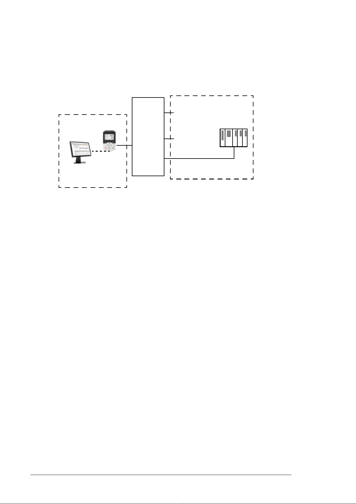
Control panel or Drive composer
PC tool (optional)
Fieldbus adapter (Fxxx) or DDCS
communication module
1) Extra inputs/outputs can be added by installing optional I/O extension modules (FIO-xx)
in the option slots of the control unit.
PLC
(= Programmable
logic controller)
I/O
1)
Drive-to-drive (D2D)
link or Embedded
fieldbus interface
External control
Local control
ACS880
Local control vs. external control
The ACS880 has two main control locations: external and local. The control location is
selected with the Loc/Rem key on the control panel or in the PC tool.
External control
When the supply unit is in external control, control commands are given through
• the I/O terminals (digital and analog inputs), or optional I/O extension modules
• the embedded fieldbus interface or an optional fieldbus adapter module
• the external (DDCS) controller interface, and/or
• the drive-to-drive link.
External references are given through the fieldbus interface, analog inputs or drive-to-drive
link.
Two external control locations, EXT1 and EXT2, are available. The user can select control
signals (e.g. start and stop) and control modes for both external control locations.
Depending on the user selection, either EXT1 or EXT2 is active at a time. Selection
between EXT1/EXT2 is done via any binary source such as a digital input or fieldbus
control word (see parameter 119.11 Ext1/Ext2 sel).
Note: Typically, ABB wires essential external control signals and status monitoring signals
of a supply unit of the cabinet-installed drive to its digital inputs and relay outputs at the
factory. We also set the parameters related to the external control signals accordingly. The
commission engineer must not change these settings or the external control does not
operate as planned. See the delivery-specific circuit diagrams.
Local control
The control commands are given from the control panel keypad or from a PC equipped
with Drive composer when the supply unit is in local control.
Local control is mainly used during commissioning and maintenance. The control panel
always overrides the external control signal sources when used in local control. When
switched to local control, the control panel Start and Stop keys override the external
Start/Stop source defined for the control program. However, to control the supply unit on
Page 19

Control locations and operating modes 19
and off by the panel, you must still have the external Run enable and Start enable signals
switched on at the appropriate digital inputs of the supply unit. See section Run enable,
Start/stop and Start enable control on page 23. Changing the control location to local can
be disabled by parameter 119.17 Local control disable.
The user can select by a parameter (149.05 Communication loss action) how the supply
unit reacts to a control panel loss or PC tool communication break.
Operating modes
The IGBT supply unit can operate in two operating modes with different types of reference:
• DC control
• power control.
In both of these modes, the reactive power reference is possible simultaneously. The
mode is selectable for each control location (Local, EXT1 and EXT2) in parameter group
119 Operation mode. For control chain diagrams for each reference type, see chapter
Control chain diagrams.
Page 20

20 Control locations and operating modes
Page 21

5
Program features
Program features 21
What this chapter contains
This chapter describes the features and I/O interface of the control program.
Overview of the control program
ACS880 IGBT supply control program controls the IGBT supply unit with an IGBT bridge
type supply module. The main functions of the control program are:
• maintain DC or active power reference,
• maintain reactive power reference,
• control external charging circuit (when used),
• control main contactor.
In addition, the control program protects the unit against overtemperature, DC or AC
overvoltage and DC undervoltage. See section Charging on page 39. The control program
also limits the active and reactive power as a function of the external temperature, and the
temperature of the IGBTs. See section Power limiting due to heat rise in the supply module
on page 34.
Page 22
22 Program features
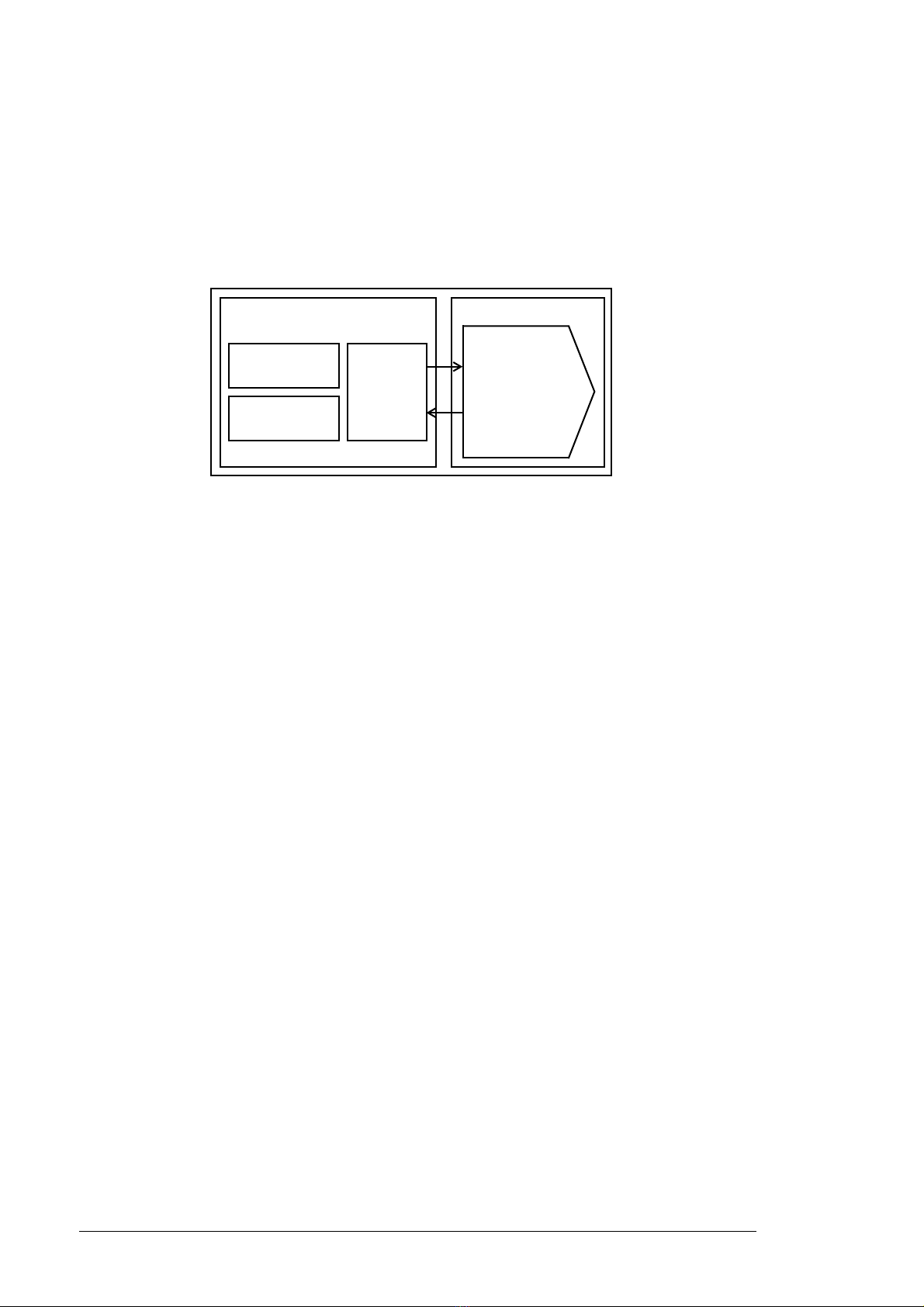
Application program Firmware
Logic
I/O interface
Fieldbus interface
Protections
Feedback
Standard
block library
Function block
program
Control program
Firmware
blocks
(parameter
interface)
Control program configuration and programming
The control program is divided into two parts:
• firmware program (forms the control program alone as standard)
• application program (addition by the customer, for special cases only).
The firmware program performs the main control functions, including handling of DC
voltage reference, reactive power reference, active power reference, supply unit logic
(start/stop), I/O, feedback, communication and protection functions. Firmware functions
are configured and programmed with parameters.
Application programming
The functions of the firmware program can be extended with application programming. (A
standard delivery does not include an application program.) Application programs can be
built out of function blocks based on the IEC 61131-3 standard using a PC tool available
separately.
For more information, see Programming manual: Drive application programming (IEC
61131-3) (3AUA0000127808 [English]).
Programming via parameters
Parameters can be set via
• the control panel, as described in chapter Using the control panel
• the Drive composer PC tool, or
• the fieldbus interface, as described in chapters Fieldbus control through the
embedded fieldbus interface (EFB) and Fieldbus control through a fieldbus adapter.
All parameter settings are stored automatically to the permanent memory of the supply
unit. However, if an external +24 V DC power supply is used for the control unit, it is highly
recommended to force a save by using parameter 196.07 Parameter save manually
before powering down the control unit after any parameter changes.
If necessary, the default parameter values can be restored by parameter 196.06
Parameter restore.
Page 23

Program features 23
Run enable, Start/stop and Start enable control
The user controls the operation of the IGBT supply unit with the Run enable command,
Start/Stop command and Start enable command. When all commands are on in the
control program, it controls the main contactor of the supply unit on with a relay output
(relay output RO3 by default), and the charging contactor/relay (relay output RO1 by
default). The main contactor connects the supply unit to the power line and the supply unit
starts rectifying. If the Start/stop command or the Run enable command is off, the control
program de-energizes the relay output and the main contactor switches off.
Note: If all supply and inverter modules connected to the common DC link have internal
charging circuits of their own, no common charging circuit in the supply unit is needed, and
the supply unit can start without doing the charging first. For more information, see section
Charging on page 39. If any of the commands is off, the control program de-energizes the
relay output and the main contactor switches off.
There is a parameter in the control program for defining the value or source for each of the
commands. By default, the parameters define the command values or sources as follows:
• Control program reads the Run enable command from digital input DI2.
• Control program reads the Start/Stop command from digital input DI2.
• Start enable is set on constantly.
Typically, DI2 is connected to the operating switch installed on the cabinet door. When the
switch is on, the control program receives both the Run enable and Start/Stop commands
via DI2.
Note: When you switch the control panel to local control, the control program starts
reading the Start/Stop from the panel (Start and Stop keys). The parameter-defined
Start/Stop source is not valid until you switch the panel back to remote control. The
Loc/Rem key of the panel selects between local and remote control.
Note: Despite of the Local/Remote mode selection by the panel, the program reads the
Run enable and Start enable from the interface defined by the appropriate parameters.
Note: Do not change the parameter settings related to Run enable, Start/Stop or Start
enable unless you are absolutely sure what you are doing. The parameters settings and
I/O wirings of the cabinet-installed unit are done at the factory according to the application
requirements.
Settings and diagnostics
Control panel key: Loc/Rem
Parameters: parameter group 119 Operation mode, 120.01 Ext1 commands…120.09 Ext2
in2 source, 120.12 Run enable 1 source, 120.19 Enable start command
Warnings: AE5A Enable start signal missing, AE5B Run enable missing
Faults: 5E06 Main contactor Fault, 3E08 LSU charging
Page 24

24 Program features
Control interfaces
Programmable analog inputs
The control unit has two programmable analog inputs. Each of the inputs can be
independently set as a voltage (0/2…10 V or -10…10 V) or current (0/4…20 mA) input by
a jumper or switch on the control unit. Each input can be filtered, inverted and scaled. The
number of analog inputs can be increased by using FIO-11 or FAIO-01 I/O extensions.
Settings and diagnostics
Parameters: parameter group 112 Standard AI
Warnings: AE27 AI parameterization
Programmable analog outputs
The control unit has two current (0…20 mA) analog outputs. Each output can be filtered,
inverted and scaled. The number of analog outputs can be increased by using FIO-11 or
FAIO-01 I/O extensions.
Settings and diagnostics
Parameters: parameter group 113 Standard AO
Programmable digital inputs and outputs
The control unit has six digital inputs, a digital start interlock input, and two digital
input/outputs.
Digital input/output DIO1 can be used as a frequency input, DIO2 as a frequency output.
The number of digital inputs/outputs can be increased by installing FIO-01, FIO-11 or
FDIO-01 I/O extensions (see Programmable I/O extensions below).
Note: Do not change the settings of the reserved digital inputs (or outputs, if any). See
subsection Reserved digital inputs and relay outputs on page 56.
Settings and diagnostics
Parameters: parameter groups 110 Standard DI, RO and 111 Standard DIO, FI, FO
Programmable relay outputs
The control unit has three relay outputs. The signal to be indicated by the outputs can be
selected by parameters. Relay outputs can be added by installing FIO-01 or FDIO-01 I/O
extensions.
Note: Do not change the settings of the reserved relay outputs. See subsection Reserved
digital inputs and relay outputs on page 56.
Settings and diagnostics
Parameters: parameter group 110 Standard DI, RO
Page 25

Program features 25
Programmable I/O extensions
The number of inputs and outputs can be increased by using I/O extension modules. The
I/O configuration parameters include the maximum number of DI, DIO, AI, AO and RO that
can be in use with different I/O extension module combinations. Slots can be added by
connecting an FEA-03 I/O extension adapter.
The table below shows the possible I/O combinations:
Digital
Location
Control unit 7 2 2 2 3
FIO-01 - 4 - - 2
FIO-11 - 2 3 1 -
FAIO-01 - - 2 2 -
FDIO-01 3 - - - 2
inputs
(DI)
Digital I/Os
(DIO)
Analog
inputs
(AI)
Analog
outputs
(AO)
Relay
outputs
(RO)
Note: Not all the FIO-xx I/O extensions are supported by the current firmware version.
(FIO-11 is supported.)
Settings and diagnostics
Parameters: parameter groups 110 Standard DI, RO, 111 Standard DIO, FI, FO,
112 Standard AI, 113 Standard AO, 114 Extension I/O module 1,
115 Extension I/O module 2, 116 Extension I/O module 3
Warnings: AE2E Extension AI parameterization, AE2F Extension I/O configuration failure
Faults: 7E00 Option module comm loss
Fieldbus control
The supply unit can be connected to an overriding control system via an optional fieldbus
adapter. See chapter Fieldbus control through a fieldbus adapter (page 235).
Settings and diagnostics
Parameters: parameter groups 150 FBA, 151 FBA A settings, 152 FBA A data in, 153 FBA
A data out, 154 FBA B settings, 155 FBA B data in, 156 FBA B data out
Warnings: AE25 FBA A parameter conflict, AE26 FBA B parameter conflict, AE30 FBA A
communication, AE31 FBA B communication
Faults: 6E01 FBA A mapping file, 6E02 FBA B mapping file, 6E0D FBA A parameter
conflict, 6E0E FBA B parameter conflict, 7E0B FBA A communication, 7E0C FBA B
communication
Page 26
26 Program features
T = Transmitter; R = Receiver
ACS880
(BCU) Control unit
RDCO
CH0
Controller
RT
RT
ACS880
(ZCU) Control unit
FDCO
RT
External controller interface
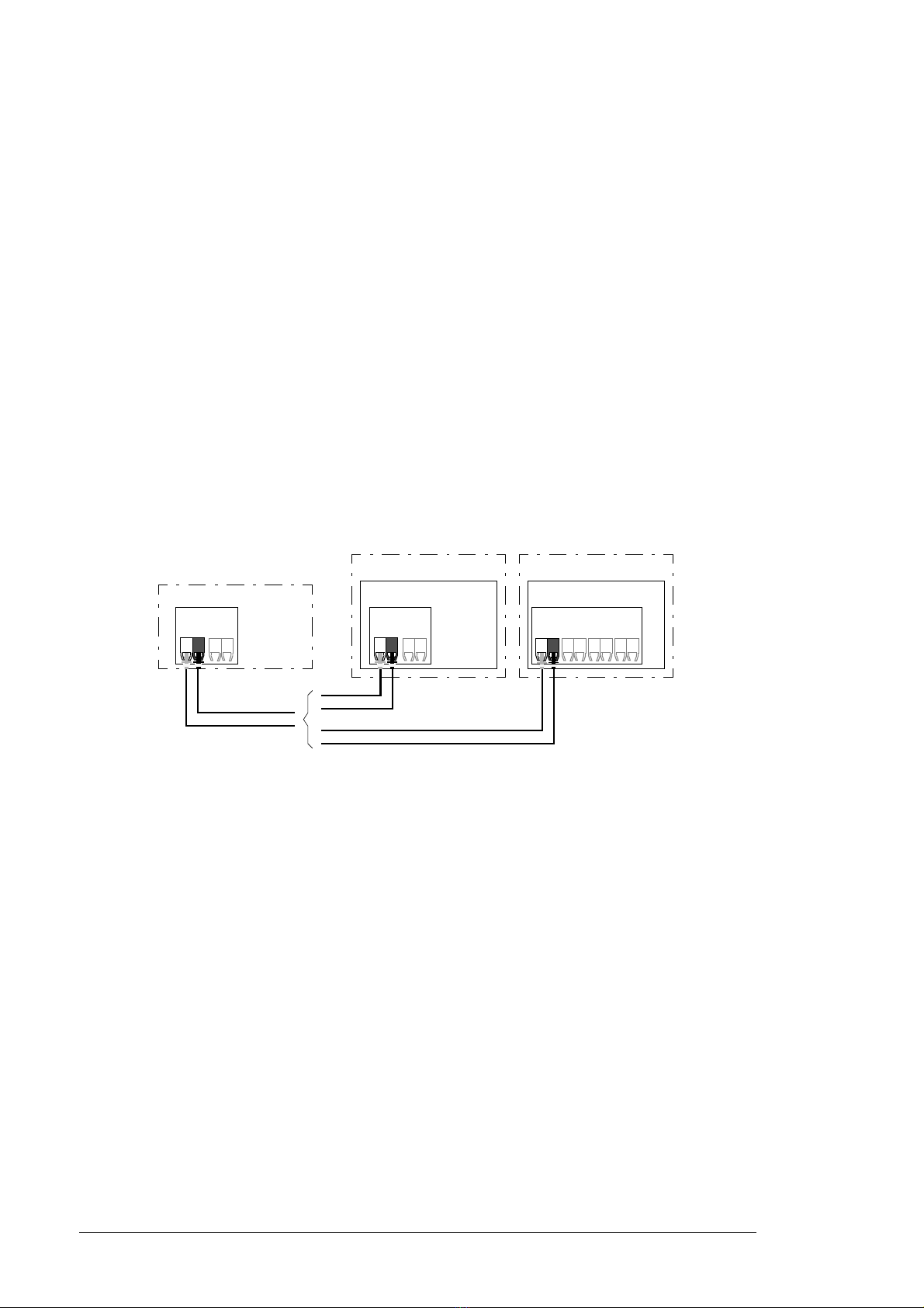
General
The IGBT supply unit can be connected to an external controller (such as the ABB
AC 800M) using either fiber optic or twisted-pair cable. The ACS880 is compatible with
both the ModuleBus and DriveBus connections. Note that some features of DriveBus
(such as BusManager) are not supported.
Topology
An example connection with either a ZCU-based or BCU-based IGBT supply unit using
fiber optic cables is shown below.
IGBT supply units with a ZCU control unit require an additional FDCO DDCS
communication module; IGBT supply units with a BCU control unit require an RDCO or
FDCO module. The BCU has a dedicated slot for the RDCO – an FDCO module can also
be used with a BCU control unit but it will reserve one of the three universal option module
slots. Ring and star configurations are also possible much in the same way as with the
master/follower link; the notable difference is that the external controller connects to
channel CH0 on the RDCO module instead of CH2. The channel on the FDCO
communication module can be freely selected.
Communication
The communication between the controller and the IGBT supply unit consists of data sets
of three 16-bit words each. The controller sends a data set to the IGBT supply unit, which
returns the next data set to the controller.
The communication uses data sets 10…33. The contents of the data sets are freely
configurable, but data set 10 typically contains the control word, while data set 11 returns
the status word and selected actual values.
The word that is defined as the control word is internally connected to the logic; the coding
of the bits is as presented in section Contents of the fieldbus Control word (page 239).
Likewise, the coding of the status word is as shown in section Contents of the fieldbus
Status word (page 240).
Page 27
Program features 27
3 3 . 1
3 2 . 1
3 2 . 2
3 3 . 3
3 2 . 3
3 3 . 2
1 9 . 0 1
1 2 3 4
1
2 4 . 0 3 4 3 0 0
.
.
.
.
.
.
.
.
.
.
.
.
Data set
Data set
Data set
Data set
Data set
Data set
Par.
Value
Parameter write to ISU
Parameter read from ISU
Transmit address
Value = 37653*
Transmit data
Value = 1234
Transmit address
feedback
Value = 37653*
Inquire address
Value = 37654**
Inquired data
Value = 4300
Inquire address
feedback
Value = 37654**
Controller ACS880
*147.21 -> 93h.15h -> 9315h -> 37653
**147.22 -> 93h.16h -> 9316h -> 37654
147.21
147.22
By default, data sets 32 and 33 are dedicated for the mailbox service, which enables the
setting or inquiry of parameter values as follows:
By parameter 160.64 Mailbox dataset selection, data sets 24 and 25 can be selected
instead of data sets 32 and 33.
The update intervals of the data sets are as follows:
• Data sets 10…11: 2 ms
• Data sets 12…13: 4 ms
• Data sets 14…17: 10 ms
• Data sets 18…25, 32, 33: 100 ms.
Settings
Parameter groups 160 DDCS communication (page 151), 161 DDCS transmit (page 158)
and 162 DDCS receive (page 162).
Page 28

28 Program features
Reference chains
Reference chains of the control program are
• DC voltage reference chain,
• active power reference chain, and
• reactive power reference chain.
Tasks of the reference chains are reference source and type selection, limitation and
ramping. The active power, DC voltage and reactive power reference chains are controlled
by reference chain control. All of the reference chains are controlled by the bits of limit
word (130.01).
DC voltage control
DC voltage is controlled by the DC voltage reference chain. DC voltage control is the
default control mode of the supply unit. It is also the alternative control mode for the active
power control. DC voltage control includes DC voltage reference selection, limitation and
ramping. Incoming DC reference is limited between maximum and minimum of the DC
limits. If the incoming reference exceeds the defined limits, the limit word is updated. DC
reference is ramped according to DC ramp up and DC ramp down times.
Control chain diagram
See page 248.
Internal DC voltage reference
Lowest possible DC voltage level in IGBT supply unit is defined by AC voltage level. If DC
voltage reference is lower than what the IGBT supply unit can achieve with control,
reference is limited internally to the lowest possible value. Minimum DC voltage reference
is filtered with 10 second time constant to prevent immediate drop in DC voltage reference
while AC voltage level drops. See also the table on page 47.
Settings and diagnostics
Parameters: parameter groups 123 DC voltage reference and 130 Limits
Active power control
Active power is controlled by the power reference chain. Active power control is an
alternative main control mode for the IGBT supply unit with the DC voltage control (which
is the default control mode of the supply unit). Power reference chain includes reference
selection, limitation and ramping.
The power reference modifies the input reference to active current reference for the ramp
function. Possible input reference types are:
• Active current reference in Amperes
• Active current reference in percent of the nominal current
• Power reference in kW
• Power reference in percent of the nominal power.
Main tasks of active current ramping are:
• Active current reference limitation
• Active current reference ramping.
The control program contains a limitation feature for limiting the active power based on
ambient temperature or the temperature of the IGBTs. The user can tune the limitation
parameters.
Page 29

Program features 29
Control chain diagram
See page 249.
Settings and diagnostics
Parameters: parameter groups 122 Power reference and 130 Limits
Reactive power control
Reactive power is controlled by the reactive power reference chain. Reactive power (or
current) control is the secondary control mode for the IGBT supply unit, and it is executed
in parallel with either of the main control options (DC voltage control or active power
control). If the IGBT supply unit is at its current limit, reactive power is limited before active
power. Reactive power reference chain includes reference selection, limitation and
ramping.
The reactive power reference modifies the input reference to reactive current reference.
Possible input reference types are:
• Reactive current reference in Amperes
• Reactive current reference in percent of the nominal current
• Reactive power reference in kVAr
• Reactive power reference in percent of the nominal power
• Reactive power reference angle in degrees
• Reactive power reference in cosphi
• Voltage reference for the AC voltage control in Volts
• Voltage reference for the AC voltage control in percent.
The type of the reactive power reference is selected with parameter.
Main tasks of the reactive current ramping are:
• Reactive current reference limitation
• Reactive current reference ramping
• Ramp bypass in case of AC voltage control.
In reactive current reference limiting the incoming reference is limited between maximum
and minimum of the reactive current limits. If the incoming reference exceeds the defined
limits, the limit word is updated. The limited output is the input signal for the ramping
function.
The control program also contains a limitation feature for limiting the reactive power based
on ambient temperature or the temperature of the IGBTs. The user can tune the limitation
parameters.
Control chain diagram
See page 250.
Settings and diagnostics
Parameters: parameter groups 124 Reactive power reference and 130 Limits
Page 30

30 Program features
Net lost detection
The IGBT supply unit recognizes the loss of supply AC voltage and recovers automatically
when the AC voltage is connected again. The supply AC lost detection is based on fast
(about 0.2 s, 10 Hz) frequency change of the grid frequency. When the frequency goes
outside the frequency limits (+
activates the net lost state and generates a warning (AE78 Net lost). When the net lost is
detected, there are two options:
• If the grid measurements from external BAMU measuring board are not available,
after the delay (default 0.1 s) the IGBT supply unit tries to resynchronize to the grid. If
resynchronization is not successful and the net lost lasts too long (default 5 s), the
IGBT supply unit trips to a fault (8E07 Net lost).
• If the grid measurements from external BAMU measuring board are available, after
the delay (default 0.1 s) the IGBT supply unit tries to resynchronize to the grid when
the grid voltages are connected again and the frequency has been estimated to be
between allowed limits. If the maximum duration of the net lost is exceeded, the IGBT
supply unit trips to a fault (8E07 Net lost).
Settings and diagnostics
Warnings: AE78 Net lost
10 Hz of the nominal frequency), the control program
Faults: 3E05 DC link undervoltage, 8E07 Net lost
Reduced run function
Reduced run function is available for IGBT supply units consisting of parallel-connected
IGBT supply modules of frame size R8i. The function makes it possible to continue
operation with limited current even if one (or more) module is out of service, for example,
because of maintenance work. In principle, reduced run is possible with only one module,
but in practice, the modules in service must be able to provide enough current for running
the inverter modules.
The number of removed IGBT supply modules and LCL filter modules is restricted. The
following table lists the allowed configurations.
Original configuration Allowed configurations when using reduced run function
2×R8i + 1×LCL 1×R8i + 1×LCL
3×R8i + 2×LCL 2×R8i + 2×LCL
4×R8i + 2×LCL 2×R8i + 1×LCL or 1×R8i + 1×LCL
6×R8i + 3×LCL 4×R8i + 2×LCL or 2×R8i + 1×LCL or 1×R8i + 1×LCL
8×R8i + 4×LCL 6×R8i + 3×LCL or 4×R8i + 2×LCL or 2×R8i + 1×LCL or 1×R8i + 1×LCL
10×R8i + 5×LCL 8×R8i + 4×LCL or 6×R8i + 3×LCL or 4×R8i + 2×LCL or 2×R8i + 1×LCL or
1×R8i + 1×LCL
Note: When IGBT supply modules and LCL filter modules are removed, the corresponding
AC fuses need to be removed too.
Page 31

Program features 31
Activation of the reduced run function
Note: For cabinet-built drives, the wiring accessories and the air baffle needed during the
procedure are available from ABB, and are included in the delivery.
WARNING! Follow the safety instructions provided for the IGBT supply
unit in question.
1. Disconnect the supply voltage and all other sources that can supply the DC bus (eg,
DC/DC converter) from the IGBT supply unit.
2. If the control unit of the IGBT supply unit is powered from the faulty module, install an
extension to the wiring and connect it to one of the remaining modules.
3. Remove the module to be serviced from its bay. See the appropriate hardware manual
for instructions.
4. Install an air baffle to the top module guide to block the airflow through the empty
module bay.
5. Switch on the power to the IGBT supply unit.
6. Enter the number of IGBT supply modules present into parameter 195.13 Reduced
run mode.
7. Reset all faults and start the IGBT supply unit. The maximum current is now
automatically limited according to the new configuration. A mismatch between the
number of detected modules and the value set in 195.13 will generate a fault (5E0E
Reduced run).
After all modules have been reinstalled, parameter 195.13 Reduced run mode must be
reset to 0 to disable the reduced run function.
Settings and diagnostics
Parameters: 195.13 Reduced run mode, 195.14 Connected modules
Faults: 5E0E Reduced run
Page 32

32 Program features
Programmable protection functions
Emergency stop
The emergency stop signal is connected to the input selected by parameter 121.05
Emergency stop source. An emergency stop can also be generated through fieldbus
(parameter 106.01 Main control word, bits 1…2).
The way the IGBT supply unit is stopped when an emergency stop command is received,
is selected with parameter 121.04 Emergency stop mode. The following selections are
available:
• stop and warning,
• warning,
• fault.
Notes:
• The installer of the equipment is responsible for installing the emergency stop devices
and all additional devices needed for the emergency stop function to fulfill the required
emergency stop categories. For more information, contact your local ABB
representative.
• After an emergency stop signal is detected, the emergency stop function cannot be
canceled even though the signal is canceled.
Settings and diagnostics
Parameters: 121.04 Emergency stop mode, 121.05 Emergency stop source
Warnings: AE68 Emergency stop warning
Faults: 6E1C Emergency stop fault
External events
An external event signal can be connected to a selectable input which is not used for other
purposes. When the signal is lost, an external event (fault, warning, or a mere log entry) is
generated.
Settings and diagnostics
Parameters: 131.01 External event 1 source…131.10 External event 5 type
Warnings: AE51 External warning 1…AE55 External warning 5
Faults: 9E01 External fault 1…9E05 External fault 5
Earth fault detection
The earth fault detection function is based on sum current measurement. Note that
• in a grounded supply, the protection activates in 200 ms,
• in an ungrounded supply, the supply network capacitance should be 1 μF or more,
• the protection is deactivated when the supply unit is stopped.
Settings and diagnostics
Parameters: 131.20 Earth fault
Warnings: AE02 Earth leakage
Faults: 2E01 Earth leakage
Page 33

Program features 33
External earth leakage fault source selection
The parameter selects in which digital input or digital input/output external earth leakage
fault is connected.
Parameters: 131.28 Ext earth leakage signal source
Faults: 2E08 External earth fault
External earth leakage action selection
The parameter selects how the IGBT supply unit reacts when an external earth leakage is
detected.
Parameters: 131.29 Ext earth leakage action
Faults: 2E08 External earth fault
Warnings: AE87 Ext earth leakage
Supply phase loss detection
The parameter selects how the supply unit reacts whenever a supply phase loss is
detected.
Settings and diagnostics
Parameters: 131.21 Supply phase loss
Faults: 3E00 Input phase loss
Local control loss detection
The parameter selects how the supply unit reacts to a control panel or PC tool
communication break.
Settings and diagnostics
Parameters: 149.05 Communication loss action
Faults: 7E01 Panel loss
Automatic fault resets
The supply unit can automatically reset itself after overcurrent, DC overvoltage, DC
undervoltage, and external faults. The user can also specify a fault that is automatically
reset.
By default, automatic resets are off and must be specifically activated by the user.
Settings and diagnostics
Parameters: 131.12 Autoreset selection…131.16 Delay time
Warnings: AE57 Autoreset
Page 34

34 Program features
Thermal switch monitoring
The control program has a thermal switch monitoring function. The function monitors the
status of the switch through a digital input typically. By default, digital input DI1 is used for
monitoring the status of the thermal switch. Multiple switches must be connected in series.
The commissioning engineer can activate the function and define the monitored input by a
parameter. If the function receives an overtemperature indication (DI1 = 0), it trips the
supply unit to a fault.
Settings and diagnostics
Parameters: 131.33 Cabinet temperature fault source, 131.34 Cabinet temperature
supervision
Faults: 4E06 Cabinet or LCL overtemperature
Power limiting due to heat rise in the supply module
The control program has a supply module temperature monitoring function. The
commissioning engineer can define:
• the source for the coolant temperature measurement
• active and reactive power profile vs. temperature value
• warning and fault trip limits.
The function monitors the temperature of the coolant exiting the module. When the value
reaches the limit defined for the power limiting profile, the control program starts limiting
the power. If the temperature keeps rising despite of the power limiting, the control
program generates first a warning (at warning limit), and then trips to a fault (at fault limit).
User can activate and tune limitation in parameter group 130 Limits.
Example
Set parameter 130.50 Ext Tmp1 input selection with selection Other to 114.26 AI1 actual
value. Set parameter 114.77 AO1 source with selection Other to 130.54 Pt current. It is
possible to use groups 115 or 116 also.
Settings and diagnostics
Parameter groups: 130 Limits, 114 Extension I/O module 1…116 Extension I/O module 3
Warnings: AE10 Ext Tmp1 warning, AE11 Ext Tmp2 warning
Counting the number of charging attempts
The control program monitors charging attempts to prevent charging circuit overheating.
Settings and diagnostics
Parameters: 120.50 Charging overload event sel
Warnings: AE85 Charging count
Faults: 3E09 Charging count
Page 35

Program features 35
DC overvoltage and undervoltage protections
The control program defines the DC overvoltage and undervoltage limits on basis of the
supply voltage range given by the user with a parameter (195.01). The program monitors
the actual voltage level with an internal voltage measurement. When the measured value
exceeds the overvoltage limit or falls below the undervoltage limit, the control program
trips to a fault.
Trip limits
The trip limits of the intermediate DC link voltage are relative to the supply voltage range
selected with parameter 195.01 Supply voltage as well as supply unit type. The DC
voltage is displayed by parameter 101.01 DC voltage. The following table shows the
values of selected DC voltage levels in Volts.
Fault limit type
Overvoltage fault limit (R1i…R6i,
xxxxA-3)
Overvoltage fault limit (R1i…R6i,
xxxxA-5)
Overvoltage fault limit (R8i, xxxxA-3) 859.5 - - - -
Overvoltage fault limit (R8i, xxxxA-5) 859.5 895.5 895.5 - -
Overvoltage fault limit (R8i, xxxxA-7) - - - 1293 1293
Undervoltage fault limit (all types) 308 357 405 425 535
380…415 V 440…480 V 500 V 525…600 V 660…690 V
844----
880 880 880 - -
Supply voltage range (195.01)
Boost limits
Boost limit depends on the maximum voltage of the power module. Boost limits for DC
voltage are given in the table below.
DC voltage reference range
IGBT supply module type
xxxxA-3
xxxxA-5
xxxxA-7
Minimum
[V]
1)
1)
1)
Maximum
[V]
2)
663
2)
799
2)
110 2
1)
The control program limits the minimum value to sqrt(2) × Uac × (1.03…1.08).
2)
The maximum value is limited by parameter 123.06 DC voltage ref max.
Settings and diagnostics
Parameters: 101.01 DC voltage, 123.06 DC voltage ref max, 195.01 Supply voltage
Warnings: AE09 DC link overvoltage, AE0A DC link undervoltage
Faults: 3E04 DC link overvoltage, 3E05 DC link undervoltage
Page 36

36 Program features
Percentage of samples
0…10%
10…20%
20…30%
30…40%
40…50%
50…60%
60…70%
70…80%
80…90%
>90%
Amplitude ranges (parameters 136.40…136.49)
Diagnostics
Maintenance timers and counters
The program has six different maintenance timers or counters that can be configured to
generate a warning when a pre-defined limit is reached. The contents of the message can
be edited on the control panel by selecting Settings - Edit texts.
The timer/counter can be set to monitor any parameter. This feature is especially useful as
a service reminder.
There are three types of counters:
• On-time timers. Measures the time a binary source (for example, a bit in a status
word) is on.
• Signal edge counters. The counter is incremented whenever the monitored binary
source changes state.
• Value counters. The counter measures, by integration, the monitored parameter. A
warning is given when the calculated area below the signal exceeds a user-defined
limit.
Settings and diagnostics
Parameters: parameter group 133 Generic timer & counter
Load analyzer
Peak value logger
The user can select a signal to be monitored by a peak value logger. The logger records
the peak value of the signal along with the time the peak occurred, as well as supply unit
current, DC voltage and power at the time of the peak.
Amplitude loggers
The control program has two amplitude loggers.
For amplitude logger 2, the user can select a signal to be sampled at 200 ms intervals
when the IGBT supply unit is running, and specify a value that corresponds to 100%. The
collected samples are sorted into 10 read-only parameters according to their amplitude.
Each parameter represents an amplitude range 10 percentage points wide, and displays
the percentage of the collected samples that fall within that range.
Page 37

Program features 37
Amplitude logger 1 is fixed to monitor the converter current, and cannot be reset. With
amplitude logger 1, 100% corresponds to the maximum output current (I
distribution of samples is shown by parameters 136.20…136.29.
Settings
Parameters: parameter group 136 Load analyzer
max
). The
User parameter sets
The IGBT supply unit supports four user parameter sets that can be saved to the
permanent memory and recalled using parameters. It is also possible to use digital inputs
to switch between user parameter sets.
A user parameter set contains all editable values in parameter groups 110…199 except
• I/O extension module settings (groups 114…116)
• data storage parameters (group 147), and
• fieldbus communication settings (groups 151…156).
Settings and diagnostics
Parameters 196.10…196.13 (page 172).
User lock
For better cybersecurity, it is highly recommended that you set a master pass code to
prevent eg, the changing of parameter values and/or the loading of firmware and other
files.
WARNING! ABB will not be liable for damages or losses caused by the failure to
activate the user lock using a new pass code. See Cybersecurity disclaimer (page
12).
To activate the user lock for the first time, enter the default pass code, 10000000, into
196.02 Pass code. This will make parameters 196.100…196.102 visible. Then enter a new
pass code into 196.100 Change user pass code, and confirm the code in 196.101 Confirm
user pass code. In 196.102 User lock functionality, define the actions that you want to
prevent (we recommend you select all the actions unless otherwise required by the
application).
To close the user lock, enter an invalid pass code into 196.02 Pass code, activate 196.08
Control board boot, or cycle the power. With the lock closed, parameters
196.100…196.102 are hidden.
To reopen the lock, enter your pass code into 196.02 Pass code. This will again make
parameters 196.100…196.102 visible.
Settings
Parameters 196.02 (page 171) and 196.100…196.102 (page 175).
Page 38

38 Program features
Data storage parameters
Twenty-four (sixteen 32-bit, eight 16-bit) parameters are reserved for data storage. These
parameters are unconnected and can be used for linking, testing and commissioning
purposes. They can be written to and read from using other parameters’ source or target
selections.
Settings and diagnostics
Parameters: parameter group 147 Data storage
Page 39

Program features 39
Charging
The charging is always needed to power up the DC link capacitors smoothly. In other
words: you may not connect the discharged capacitors to full supply voltage but you must
increase the voltage gradually until the capacitors are charged and ready for normal use.
The control program has a function for controlling an additional charging circuit in the IGBT
supply unit. The charging function is active as standard, since the cabinet-installed ABB
drive which uses IGBT supply unit, needs the additional charging circuit typically.
Note: Some ABB supply and inverter module sizes have internal charging circuit as
standard. (Check from the appropriate supply and inverter module hardware manuals.) If
all supply and inverter modules connected to the common DC link of the drive have the
internal charging circuit, you do not need the common, additional circuit in the supply unit.
Then you can also inactivate the charging function of the supply unit (a parameter setting).
When the control program receives the start command (and Run enable and Start enable
are on), the control program controls the charging contactor on by a relay output. The
contactor connects the input power line to the drive DC link via charging resistors. The DC
capacitor charging starts. The DC voltage level in the DC link increases as the charging
continues. The charging resistors limit the charging current.
Charging is completed when:
• the actual DC voltage exceeds the predefined level (parameter 120.25 MCB closing
level)
• the actual DC voltage change rate is below the predefined level (parameter 120.26
Maximum dU/dt), and
• the pre-defined delay time has passed (parameter 120.27 Start delay).
The control program monitors the charging time. If charging takes more time than defined
by a parameter, the supply unit trips to a fault.
If the IGBT supply unit is used in a drive system where the charging must be done by the
IGBT supply unit, you must install an additional charging circuit, and activate and tune the
charging function in the IGBT supply control program. Consult ABB for more information
on tuning the parameters, and the components and wirings needed.
The control program checks that voltage rises after the charging contactor is closed. If the
voltage does not rise and the current stays below the level defined with parameter 120.22
Max current for MCB closing, the supply unit trips on fault 3E08 LSU charging (auxiliary
code 5). If the current is higher, the supply unit trips on fault 2E09 DC short circuit.
The control program monitors charging attempts to prevent charging circuit overheating. If
there are more than two attempts in five minutes to charge the DC link externally, start
inhibit is set (106.18 Start inhibit status word, bit 9). After five minutes from the first
charging attempt the start inhibit is removed. The supply unit also generates an event
selected with parameter 120.50 Charging overload event sel.
Page 40

40 Program features
1
3
1 2 3 4
1001h
1h
4
2
107h
3h
Udc 100% of nominal
120.25 MCB closing level
80% default, range
20…100%
Udc 0% of nominal
DC voltage and current
measurements are not active with
all power unit types on low DC
voltage levels in the beginning of
the charging sequence
DC voltage
Delay if 120.28 MCB relay
timing >0
0 s default, range -6…6 s
120.26 Maximum dU/dt
50.0 V/s default, range 0.0…200.0 V/s
Charging ready [conditions
passed]
Running on DC voltage control
120.22 Max current for
MCB closing
5% default, range 0…10%
106.11 Main status word
Only starting procedure related bits of the 106.11 Main
status word are shown in hexadecimal values here.
Other values of Main status word are possible
depending on control location etc. (eg, bit 9 Remote).
ON command and START
command from active control
location
110.24 RO1 source
Charging
Charging contactor closing command
Delay if 120.28 MCB relay timing <0
0 s default, range -6…6 s
110.30 RO3 source
MCB
MCB closing command
Delay if 120.28 MCB relay
timing >0
0 s default, range -6…6 s
If feedback is missing after
supervision delay, fault
5E06 Main contactor Fault is
generated.
Start delay for starting of
modulation begins after MCB
closing feedback (DI3 status is 1)
120.21 Delay for MCB DI3
supervision
1 s default, range 0…8 s
DI3 status
Running status
120.27 Start delay
0.5 s default, range 0…10 s
120.23 Max DC charging time
3 s default, range 0…10 s
Charging ready state can not be
reached before this time is
passed.
If charging ready state is not
reached before this time has
elapsed, fault 3E08 LSU
charging is generated. See
auxiliary code in chapter
Fault tracing.
Module current
4001h
Timing diagram
Settings and diagnostics
Signals: 101.01 DC voltage
Parameters: 106.18 Start inhibit status word, 110.24 RO1 source, 120.22 Max current for
MCB closing, 120.23 Max DC charging time, 120.25 MCB closing level, 120.26 Maximum
dU/dt, 120.27 Start delay, 120.28 MCB relay timing, 120.29 Diode mode, 120.30 External
charge enable, 120.50 Charging overload event sel
Warnings: AE85 Charging count
Faults: 2E09 DC short circuit, 3E08 LSU charging, 3E09 Charging count, 5E06 Main
contactor Fault
Page 41

Program features 41
DDCS communication with inverter unit
DDCS communication can be used for transferring data between IGBT supply unit and
inverter unit. The DDCS communication and the related transfer media (fiber optic link) are
in use in the single drives which consist of one supply unit and one inverter unit. The
DDCS link is not in use in multidrives, typically.
You can use the DDCS communication for these purposes:
• You can show and adjust the supply unit parameters in the inverter control program
(one interface for the control panel and commissioning engineer).
• You can show supply unit warnings and faults in the inverter control program.
• You can control both the inverter unit and the supply unit through one control interface
(for example one fieldbus adapter) in the inverter unit, and transfer the supply unit
control commands and references via the link to the supply unit.
For information on using DDCS communication, see section Setting up communication
through inverter unit on page 243.
Settings and diagnostics
Parameters: parameter groups 160 DDCS communication, 161 DDCS transmit,
162 DDCS receive
Warnings: AE56 INU-LSU comm loss
Faults: 7E0D FA2FA DDCS Com loss
Page 42

42 Program features
XD2D Drive-to-drive link
1 B
Drive-to-drive link (not in use by default)
2 A
3 BGND
4 Shield
D2D.TERM Drive-to-drive link termination
1)
X485 RS485 connection
5 B
Not in use (not in use by default)
6 A
7 BGND
8 Shield
XRO1…XRO3 Relay outputs
11 NC
XRO1: Charging
2)
(Energized = Closes charging contactor.)
250 V AC / 30 V DC / 2 A
12 COM
13 NO
21 NC
XRO2: Fault(-1)
3)
(Energized = Indicates no fault.)
250 V AC / 30 V DC / 2 A
22 COM
23 NO
31 NC XRO3: MCB ctrl
2)
(Energized = Closes main contactor/breaker.)
250 V AC / 30 V DC / 2 A
32 COM
33 NO
XSTO XSTO connector
1 OUT XSTO connector. Both circuits (power module, control unit) must be closed for
the supply unit to start. (IN1 and IN2 must be connected to OUT.)
4)
2 SGND
3 IN1
4 IN2
5 IN1
Not in use
6 SGND
7 IN2
8 SGND
XDI Digital inputs
1 DI1 Temp fault
3)
(0 = overtemperature)
2 DI2 Run / enable
3)
(1 = run / enable)
3 DI3 MCB fb
2)
(0 = main contactor/breaker open)
4 DI4 Not in use by default. Can be used for eg, auxiliary circuit breaker fault
5 DI5 Not in use by default. Can be used for eg, earth fault monitoring.
6 DI6 Reset 3) (0 -> 1 = fault reset)
7 DIIL Not in use by default. Can be used for eg, emergency stop.
XDIO Digital input/outputs
1 DIO1 Not in use by default
2 DIO2 Not in use by default
3 DIOGND Digital input/output ground
4 DIOGND Digital input/output ground
XD24 Auxiliary voltage output
5 +24VD +24 V DC 200 mA
5)
6 DICOM Digital input ground
7 +24VD +24 V DC 200 mA
5)
8 DIOGND Digital input/output ground
DICOM=DIOGND Ground selection switch
6)
XAI Analog inputs, reference voltage output
1 +VREF 10 V DC, RL 1…10 kohm
2 -VREF -10 V DC, RL 1…10 kohm
3 AGND Ground
4 AI1+ Not in use by default.
0(2)…10 V, R
in
> 200 kohm
7)
5 AI1-
6 AI2+ Not in use by default.
0(4)…20 mA, R
in
= 100 ohm
8)
7 AI2-
XAO Analog outputs
1 AO1
Zero
3)
0…20 mA, RL < 500 ohm
2 AGND
3 AO2
Zero
3)
0…20 mA, RL < 500 ohm
4 AGND
XPOW External power input
1 +24VI
24 V DC, 2.05 A
2 GND
3 +24VI
4 GND
X12 Safety functions module connection (not in use in supply units)
X13 Control panel connection
X205 Memory unit connection
Default I/O connection diagram (BCU)
Page 43

Program features 43
The table above shows the control connections of the IGBT supply unit, and the default
meaning or use of the signals in the control program. Most I/O connections are reserved
and wired for the internal use at the factory. Do not change the connections.
Wire sizes and tightening torques: 0.5 … 2.5 mm
2
(24…12 AWG) and 0.5 N·m (5 lbf·in) for
both stranded and solid wiring.
Notes:
1)
Switch D2D.TERM. Must be set to ON when the supply unit is the first or last unit on the drive-to-drive (D2D)
link. On intermediate supply units, set termination to OFF.
2)
Use of the signal in the control program. When parameter 120.30 External charge enable has value Yes
(default setting), the control program reserves this I/O terminal for external charging circuit control and
monitoring, and parameters 110.24 RO1 source and 110.30 RO3 source are write-protected. If the value is No,
you can use the I/O terminal for other purposes.
3)
Default use of the signal in the control program. The use can be changed by a parameter. For the delivery-
specific use, see the delivery-specific circuit diagrams.
4)
The Safe torque off (STO) function is only implemented in the inverter units. When the control board is used
in the supply or brake unit, de-energizing IN1 or IN2 of XSTO connector only stops the operation of the supply
or brake unit. This stopping is not safety related and can not be used in safety purposes.
5)
Total load capacity of these outputs is 4.8 W (200 mA at 24 V) minus the power taken by DIO1 and DIO2.
6)
Determines whether DICOM is separated from DIOGND (ie, common reference for digital inputs floats).
DICOM=DIOGND ON: DICOM connected to DIOGND. OFF: DICOM and DIOGND separate.
7)
Current [0(4)…20 mA, Rin= 100 ohm] or voltage [0(2)…10 V, Rin> 200 kohm] input selected by switch AI1.
Change of setting requires reboot of control unit.
8)
Current [0(4)…20 mA, Rin= 100 ohm] or voltage [0(2)…10 V, Rin> 200 kohm] input selected by switch AI2.
Change of setting requires reboot of control unit.
Page 44

44 Program features
Default I/O connection diagram (ZCU)
Relay outputs XRO1…XRO3
XRO1: Charging
1)
250 V AC / 30 V DC
2 A
XRO2: Fault (-1)
2)
250 V AC / 30 V DC
2 A
XRO3: MCB ctrl
1)
250 V AC / 30 V DC
2 A
(Energized = Closes charging contactor.)
(Energized = Indicates no fault)
(Energized = Closes main contactor/breaker.)
NO
COM 2
NC 1
NO
COM 2
NC 1
NO
COM 2
NC 1
Power supply XPOW
24 V DC, 2 A
GND
+24VI
Reference voltage and analog inputs J1, J2, XAI
AI1/AI2 current/voltage selection
Not in use by default
0(4) … 20 mA, Rin> 100 ohm
Not in use by default
0(4) … 20 mA, Rin> 100 ohm
3)
4)
AI1: U AI2: U
AI1: I AI2: I
AI2- 7
AI2+ 6
AI1- 5
AI1+ 4
Ground AGND 3
-10 V DC, RL 1 … 10 kohm -VREF 2
10 V DC, RL 1 … 10 kohm +VREF 1
Analog outputs XAO
2)
0 … 20 mA, RL < 500 ohm
Zero
2)
0 … 20 mA, RL< 500 ohm
Zero
AGND
AO2 3
AGND
AO1 1
Drive-to-drive link (not connected by default)
Shield 4
Drive-to-drive link
BGND 3
A 2
B 1
Drive-to-drive link termination
5)
XSTO circuit XSTO
IN2 4
Both circuits (power module, control unit) must be closed for the supply unit to
start. (IN1 and IN2 must be connected to out.) 6)
IN1
SGND 2
OUT 1
Digital inputs XDI
2)
Reset
(0 -> 1 = fault reset) DI6 6
Not in use by default. Can be used for eg, earth fault monitoring. DI5
Not in use by default. Can be used for eg, auxiliary circuit breaker fault. DI4 4
MCB fb
Run / enable
Temp fault
1)
(0 = main contactor/breaker open) DI3 3
2)
(1 = run / enable) DI2 2
2)
(0 = overtemperature) DI1 1
Digital input/outputs XDIO
Not in use by default DIO2 2
Not in use by default DIO1 1
Ground selection
7)
Auxiliary voltage output, digital input interlock XD24
Digital input/output ground DIOGND 5
+24 V DC 200 mA
8)
+24VD 4
Digital input ground (common) DICOM
+24 V DC 200 mA
8)
+24VD 2
Not in use by default DIIL
Safety functions module connection (not connected by default) X12
Control panel connection (connected to control panel by default) X13
Memory unit connection X205
3
3
3
2
1
4
2
XD2D
3
5
3
1
J3
J6
Page 45

Program features 45
The table above shows the control connections of the IGBT supply unit, and the default
meaning or use of the signals in the control program. Most I/O connections are reserved
and wired for the internal use at the factory. Do not change the connections.
Wire sizes and tightening torques: 0.5 … 2.5 mm
2
(24…12 AWG) and 0.5 N·m (5 lbf·in) for
both stranded and solid wiring.
Notes:
1)
Use of the signal in the control program. When parameter 120.30 External charge enable has value Yes
(default setting), the control program reserves this I/O terminal for external charging circuit control and
monitoring, and parameters 110.24 RO1 source and 110.30 RO3 source are write-protected. If the value is No,
you can use the I/O terminal for other purposes
2)
Default use of the signal in the control program. The use can be changed by a parameter. For the delivery-
specific use, see the delivery-specific circuit diagrams.
3)
Current [0(4)…20 mA, Rin> 100 ohm] or voltage [0(2)…10 V, Rin> 200 kohm] input selected by jumper J2.
Change of setting requires reboot of control unit.
4)
Current [0(4)…20 mA, Rin> 100 ohm] or voltage [0(2)…10 V, Rin> 200 kohm] input selected by jumper J1.
Change of setting requires reboot of control unit.
5)
Jumper/switch J3. Enable bus termination on the supply units at the ends of the drive-to-drive (D2D) link. On
intermediate supply units, disable bus termination.
ZCU-14: Termination disabled. Termination enabled.
6)
The Safe torque off (STO) function is only implemented in the inverter units. When the control board is used
in the supply or brake unit, de-energizing IN1 or IN2 of XSTO connector only stops the operation of the supply
or brake unit. This stopping is not safety related and can not be used in safety purposes.
7)
Jumper/switch J6. Determines whether DICOM is separated from DIOGND (ie, common reference for digital
inputs floats).
ZCU-14: DICOM connected to DIOGND. DICOM and DIOGND separate.
8)
Total load capacity of these outputs is 4.8 W (200 mA at 24 V) minus the power taken by DIO1 and DIO2.
Parameters that define the use of relay outputs
The table below shows the relay outputs and the parameters and that define their use by
default.
Output Parameter Default value
RO1 110.24 RO1 source Charging
RO2 110.27 RO2 source Fault (-1)
RO3 110.30 RO3 source MCB
Parameters that define the use of digital inputs
The table below shows the default use of digital inputs by parameters.
Input Parameter Additional information
DI1 131.33 Cabinet temperature fault source 0 = overtemperature
Typically this is used for monitoring the status of
cabinet temperature fault.
DI2 120.12 Run enable 1 source
120.03 Ext1 in1 source
DI6 131.11 Fault reset selection 0 -> 1 = fault reset
1 = run enable
1 = on
Page 46

46 Program features
The table below shows the common use of the remaining digital inputs in the cabinet
installed drives by ABB. Note that these are no default parameters settings in the control
program.
Input Parameter Additional information
DI4 131.32 Aux circuit breaker fault source 0 = auxiliary circuit breaker or switch open
Typically this is used for monitoring the status of
auxiliary circuit breaker.
DI5 131.28 Ext earth leakage signal source 0 = earth leakage current monitoring tripped
DIIL 121.05 Emergency stop source 0 = emergency stop active
For the rest of the parameters that can use digital inputs as signal source, see chapter
Parameters.
Page 47

Program features 47
0.05 ·
2/3 · 500 V 20 V
222
Power share with droop control
If two supply units that are fed from separate transformers are connected to the same DC
link, you must make sure that the power share is controlled and the system remains
stable. Always use the same DC voltage reference for all units. Use also the droop
function in all units.
The droop function stabilizes the load sharing between the units. It automatically tunes the
external DC voltage reference slightly as the actual load of the unit varies: it changes the
reference in the generating mode and in the motoring mode. See the diagram below.
When the droop is active in all units, their reference corrections help in finding the right
load balance and remain it automatically.
With the droop control enabled, two supply units can control the same DC link voltage. DC
voltage reference droop is implemented by modifying the DC link voltage reference
depending on actual power with droop rate. The droop increases the DC link voltage in
generator-side and decreases it in motoring side. Droop control is defined by parameters
123.30 Udc-ctrl droop and 123.31 Udc-ctrl drooping rate. The default drooping rate is 5%
of nominal phase peak voltage. With nominal motor-side power the DC link reference is
decreased:
Some examples of needed marginal for DC reference with 5% drooping rate are given in
the table below. See also the diagram below.
AC line voltage DC voltage Minimum DC
voltage
415 V 616 V
500 V 742 V
690 V 1025 V
·415·1.05
·500·1.05
·690·1.05
Droop marginal DC reference (see
parameter 123.01)
17 V 616 V +17 V = 633 V
20 V 742 V + 20 V = 762 V
28 V 1025 V + 28 V = 1053 V
If the AC grid voltage is higher, more marginal is needed since phase-to-phase peak grid
voltage is the lowest DC voltage that the supply unit can produce. Producing capacitive
reactive power requires DC voltage and DC voltage marginal that are higher than usual
default values. See also section Reactive power control on page 29.
Page 48

48 Program features
650 V
-100% 100%
633 V
0V
DC voltage (V)
Maximum DC voltage reference
Power (% of nominal)
Minimum DC
voltage reference
2)
1)
1) 616 V (calculated from nominal DC voltage with 5% modulation margin)
2) 663 V (113% of nominal DC voltage)
Example from the table (page 47) with 415 V AC voltage
Nominal DC voltage 587 V (parameter 101.62)
The following figure shows an example of drooping.
Difference in voltage measurements of the IGBT supply units causes error in power share
between the units. This error can be corrected with parameter 123.13 DC voltage ref add.
Then check with the load also. In master/follower communication the correction is done
automatically when the master sends the actual value of the power to the follower.
Example:
Increase the reference by 0.25 V in that IGBT supply unit that takes less power
or vice versa.
See also Parallel-connected ACS880-207 IGBT supply units system description
(3AXD50000032517 [English]).
Master/follower link
The supply units have a master/follower link between them. The link is built by connecting
the units together with fiber optic cables. The communication on the link is based on the
DDCS protocol, and there are RDCO communication modules on the BCU control units of
both supply units to organize DDCS communication.
Before start
Droop must be enabled from all supply units feeding the same DC link. See parameter
123.30 Udc-ctrl droop. When drooping is used, the user-given DC voltage reference
(source 123.02 DC voltage ref selection) needs to be increased from internally calculated
default value so that the droop control can decrease the DC voltage.
Settings
Parameters: 123.13 DC voltage ref add, 123.30 Udc-ctrl droop, 123.31 Udc-ctrl drooping
rate
Page 49

Program features 49
Master/follower functionality
General
The master/follower functionality can be used to link several supply units together so that
the load can be evenly distributed between them.
The external control signals are typically connected to one supply unit only which acts as
the master. The master controls up to 10 followers by sending broadcast messages over
an electrical cable or fiber optic link. The master can read feedback signals from up to 3
selected followers.
The operating mode can be selected by parameter (119.12 Ext1 ctrl mode1 or 119.14 Ext2
ctrl mode1). See chapter Control locations and operating modes (page 17).
If a supply unit needs to quickly switch between master and follower statuses, one user
parameter set (see page 37) can be saved with the master settings, another with the
follower settings. The suitable settings can then be activated using eg, digital inputs. For
more information on redundant system, see Parallel-connected ACS880-207 IGBT supply
units system description (3AXD50000032517 [English]).
Communication
A master/follower link can be built by connecting the units together with fiber optic cables
(may require additional equipment depending on existing hardware), or by wiring together
the XD2D connectors of the units. The medium is selected by parameter 160.01 M/F
communication port. Parameter 160.03 M/F mode defines whether the unit is the master
or a follower on the communication link.
The communication on the master/follower link is based on the DDCS protocol, which
employs data sets (specifically, data set 41). One data set contains three 16-bit words. The
contents of the data set are freely configurable using parameters 161.01…161.03. The
data set broadcast by the master typically contains the control word and the references,
while the followers return a status word with two actual values.
The default setting of parameter 161.01 M/F data 1 selection is Follower CW. With this
setting in the master, a word consisting of bits 0…11 of 106.01 Main control word is
broadcast to the followers. However, bit 3 of the follower control word is modified so that it
remains on as long as the master is modulating, and its switching to 0 causes the follower
to stop modulating. This is to synchronize the stopping of both master and follower.
Three words of additional data can optionally be read from each follower. The followers
from which data is read are selected by parameter 160.14 M/F follower selection in the
master. In each follower, the data to be sent is selected by parameters 161.01…161.03.
The data is transferred in integer format over the link, and displayed by parameters
162.28…162.36 in the master. The data can then be forwarded to other parameters using
162.04…162.12.
To indicate faults in the followers, each follower must be configured to transmit its status
word as one of the above-mentioned data words. In the master, the corresponding target
parameter must be set to Follower SW. The action to be taken when a follower is faulted is
selected by 160.17 Follower fault action. External events (see parameter group 131 Fault
functions) can be used to indicate the status of other bits of the status word.
Page 50

50 Program features
Master/follower wiring with electrical cable
Master
Termination ON
1
2
3
4
1
2
3
4
1
2
3
4
XD2D
B
XD2D
XD2D
A
BGND
Shield
B
A
BGND
Shield
B
A
BGND
Shield
Follower 1
Termination OFF
Follower n
Termination ON
See the hardware manual for wiring and termination details.
Ring configuration with fiber optic cables
T = Transmitter; R = Receiver
Follower 2
(ZCU) Control unit
FDCO
RT
Follower 1
(BCU) Control unit
RDCO
RT
CH2
Master
(ZCU) Control unit
FDCO
RT
Construction of the master/follower link
The master/follower link is formed by connecting the units together using either
• shielded twisted-pair cable between the XD2D terminals*, or
• fiber optic cables. Supply units with a ZCU control unit require an additional FDCO
DDCS communication module; supply units with a BCU control unit require an RDCO
module.
*This connection cannot co-exist, and is not to be confused with, drive-to-drive (D2D)
communication implemented by application programming (detailed in Drive application
programming manual (IEC 61131-3), 3AUA0000127808 [English]).
Connection examples are shown below. Note that a star configuration using fiber optic
cables requires an NDBU-95C DDCS branching unit.
Page 51

Program features 51
Follower 3
(ZCU) Control unit
FDCO
Follower 1
Star configuration with fiber optic cables (1)
T = Transmitter
R = Receiver
NDBU
MSTR CH0 CH1 CH2
R T R T R T R T
RT
(ZCU) Control unit
Follower 2
(BCU) Control unit
RDCO
RT
CH2
FDCO
RT
Master
(ZCU) Control unit
FDCO
RT
Follower 3
(ZCU) Control unit
FDCO
Follower 1
Star configuration with fiber optic cables (2)
T = Transmitter
R = Receiver
NDBU
CHx CHx
R T R T
RT
(ZCU) Control unit
Follower 2
(BCU) Control unit
RDCO
RT
CH2
FDCO
RT
Master
(ZCU) Control unit
FDCO
RT
CHx CHx
R T R T
X13 = REGEN
Page 52

52 Program features
Example parameter settings
The following is a checklist of parameters that need to be set when configuring the
master/follower link. In this example, the master broadcasts the Follower control word and
the references. The follower returns a status word and two actual values (this is not
compulsory but is shown for clarity).
Master settings
:
• Master/follower link activation
• 160.01 M/F communication port (fiber optic channel or XD2D selection)
• (160.02 M/F node address = 1)
• 160.03 M/F mode = DDCS master (for both fiber optic and wire connection)
• 160.05 M/F HW connection (Ring or Star for fiber optic, Star for wire)
• Data to be broadcast to the followers
• 161.01 M/F data 1 selection = Follower CW (Follower control word)
• 161.02 M/F data 2 selection = Master power
• Data to be read from the followers (optional)
• 160.14 M/F follower selection (selection of followers that data is read from)
• 162.04 Follower node 2 data 1 sel … 162.12 Follower node 4 data 3 sel (mapping
of data received from followers)
Follower settings
:
• Master/follower link activation
• 160.01 M/F communication port (fiber optic channel or XD2D selection)
• 160.02 M/F node address = 2…60
• 160.03 M/F mode = DDCS follower (for both fiber optic and wire connection)
• 160.05 M/F HW connection (Ring or Star for fiber optic, Star for wire)
• Mapping of data received from master
• 162.01 M/F data 1 selection = CW 16bit
• 162.02 M/F data 2 selection = Ref1 16bit
• 162.03 M/F data 3 selection = Ref2 16bit
• Selection of operating mode
• 119.12 Ext1 ctrl mode1 = DC control or Power control
• Selection of data to be sent to master (optional)
• 161.01 M/F data 1 selection = SW 16bit
• 161.02 M/F data 2 selection = Act1 16bit
• 161.03 M/F data 3 selection = Act2 16bit
Page 53

Program features 53
Specifications of the fiber optic master/follower link
• Maximum fiber optic cable length:
• FDCO-01/02 or RDCO-04 with POF (Plastic Optic Fiber): 30 m
• FDCO-01/02 or RDCO-04 with HCS (Hard-clad Silica Fiber): 200 m
• For distances up to 1000 m, use two NOCR-01 optical converter/repeaters with
glass optic cable (GOF, 62.5 micrometers, Multi-Mode)
• Maximum shielded twisted-pair cable length: 50 m
• Transmission rate: 4 Mbit/s
• Total performance of the link: < 5 ms to transfer references between the master and
followers.
• Protocol: DDCS (Distributed Drives Communication System)
Settings and diagnostics
Parameter groups 160 DDCS communication (page 151), 161 DDCS transmit (page 158)
and 162 DDCS receive (page 162)
Warnings: AE81 MF comm loss, AE82 Follower
Faults: FE06 MF communication loss, FE07 Follower drive failure
Page 54

54 Program features
Page 55

6
Parameters
Parameters 55
What this chapter contains
The chapter describes the parameters, including actual signals, of the control program.
Terms and abbreviations
Term Definition
Actual signal Type of parameter that is the result of a measurement or calculation by the IGBT supply
unit, or contains status information. Most actual signals are read-only, but some
(especially counter-type actual signals) can be reset.
Def (In the following table, shown on the same row as the parameter name)
The default value of a parameter.
FbEq16 (In the following table, shown on the same row as the parameter range, or for each
selection)
16-bit fieldbus equivalent: The scaling between the value shown on the panel and the
integer used in fieldbus communication when a 16-bit value is selected for transmission
to an external system.
A dash (-) indicates that the parameter is not accessible in 16-bit format.
The corresponding 32-bit scalings are listed in chapter Additional parameter data (page
177).
Other The value is taken from another source.
Parameter Either an user-adjustable operating instruction for the IGBT supply unit, or an actual
signal.
p.u. Per unit
Page 56

56 Parameters
Reserved digital inputs and relay outputs
For the cabinet-installed unit, digital inputs and relay outputs are typically defined in use
and connected to the appropriate control circuits already at the factory. Do not change the
settings of the reserved digital inputs or relay outputs. See the delivery-specific circuit
diagrams and subsections Default I/O connection diagram (BCU) on page 42, and Default
I/O connection diagram (ZCU) on page 44.
Page 57

Parameters 57
Summary of parameter groups
Group Contents Page
101 Actual values Basic signals for monitoring of the IGBT supply unit. 58
103 Input references Values of references received from various sources. 60
104 Warnings and faults Information on warnings and faults that occurred last. 61
105 Diagnostics Various run-time-type counters and measurements related to IGBT
supply unit maintenance.
106 Control and status words Control and status words. 67
107 System info Hardware and firmware information. 73
110 Standard DI, RO Configuration of digital inputs and relay outputs. 74
111 Standard DIO, FI, FO Configuration of digital input/outputs and frequency inputs/outputs. 78
112 Standard AI Configuration of standard analog inputs. 80
113 Standard AO Configuration of analog outputs. 83
114 Extension I/O module 1 Configuration of I/O extension module 1. 86
115 Extension I/O module 2 Configuration of I/O extension module 2. 101
116 Extension I/O module 3 Configuration of I/O extension module 3. 105
119 Operation mode Selection of external control location sources and operating
modes.
120 Start/stop Start/stop and run/start enable signal source selection; charging
settings.
121 Start/stop mode Emergency stop settings. 114
122 Power reference Settings of the active power reference chain. 114
123 DC voltage reference Settings of the DC voltage reference chain. 116
124 Reactive power reference Settings of the reactive power reference chain. 117
130 Limits Operation limits of the IGBT supply unit. 121
131 Fault functions Settings that define the behavior of the IGBT supply unit upon fault
situations.
133 Generic timer & counter Configuration of maintenance timers/counters. 130
136 Load analyzer Peak value and amplitude logger settings. 136
146 Monitoring settings Scaling settings. 139
147 Data storage Parameters that can be written to and read from by using source
and target settings of other parameters.
149 Panel port communication Communication settings for the control panel port. 142
150 FBA General settings for fieldbus communication configuration. 142
151 FBA A settings Fieldbus adapter A configuration. 147
152 FBA A data in Selection of data to be transferred from IGBT supply unit to
fieldbus controller through fieldbus adapter A.
153 FBA A data out Selection of data to be transferred from fieldbus controller to IGBT
supply unit through fieldbus adapter A.
154 FBA B settings Fieldbus adapter B configuration. 149
155 FBA B data in Selection of data to be transferred from IGBT supply unit to
fieldbus controller through fieldbus adapter B.
156 FBA B data out Selection of data to be transferred from fieldbus controller to IGBT
supply unit through fieldbus adapter B.
160 DDCS communication DDCS communication configuration. 151
161 DDCS transmit Defines the data sent to the DDCS link. 158
162 DDCS receive Mapping of data received through the DDCS link. 162
195 HW configuration Various hardware-related settings. 169
196 System Language selection; parameter save and restore; control unit
reboot; user lock.
66
108
109
125
140
148
149
150
151
170
Page 58

58 Parameters
Parameter listing
No. Name/Value Description Def/FbEq16
101
101 Actual values
101.01 DC voltage Measured intermediate circuit voltage in Volts. -
0.00 … 2000.00 V Measured intermediate circuit voltage. See par.
101.02 Line current Estimated line current in Amperes. -
- Estimated line current. 1 = 1 A
101.03 Line current % Estimated line current in percent of the nominal value.
0.0 … 1000.0% Estimated line current in percent of the nominal value. 1 = 1%
101.04 Active current Estimated fundamental frequency active current in Amperes. -
- Estimated fundamental frequency active current. See par.
101.05 Active current % Estimated active current in percent of the nominal value. -
-1000.0 … 1000.0% Estimated active current in percent of the nominal value. 1 = 1%
101.06 Reactive current Estimated reactive current in Amperes. -
- Estimated reactive current. See par.
101.07 Reactive current % Estimated reactive current in percent of the nominal value. -
-1000.0 … 1000.0% Estimated reactive current in percent of the nominal value. 1 = 1%
101.08 Frequency Estimated frequency of power supply network. -
0.00…100.00 Hz Estimated frequency of power supply network. 100 = 1 Hz
101.09 Grid voltage Estimated voltage of power supply network in Volts. -
0.00…1000.00 V Estimated voltage of power supply network. 1 = 1 V
101.10 Apparent power Estimated apparent power in kVA. -
- Estimated apparent power. 1 = 1 kVA
101.11 Apparent power % Estimated apparent power in percent of the nominal value. -
-1000.0 … 1000.0% Estimated apparent power in percent of the nominal value. 1 = 1%
101.12 Power Estimated IGBT supply unit fundamental frequency power in
- Estimated IGBT supply unit fundamental frequency power. See par.
101.13 Power % Estimated fundamental frequency input power in percent of
-1000.0 … 1000.0% Estimated fundamental frequency input power in percent of
101.14 Reactive power Estimated reactive power in kVAr.
- Estimated reactive power. See par.
101.15 Reactive power % Estimated reactive power in percent. -
-1000.0 … 1000.0% Estimated reactive power in percent. 1 = 1%
101.16 CosPhi Cos phi. -
-1.00 … 1.00 Cos phi. 100 = 1
Basic signals for monitoring of the IGBT supply unit.
All parameters in this group are read-only unless otherwise
noted.
146.04
146.01
146.02
-
kW. Sign can be changed with parameter 130.47 Power sign
change.
(positive = power flow from power supply network to
intermediate circuit,
negative = power flow from intermediate circuit to power
supply network)
146.01
-
the nominal value.
1 = 1%
the nominal value.
-
(positive = capacitive, negative = inductive)
146.02
Page 59

Parameters 59
Relative
reactive
power
Relative active power
10
20
30
40
50
60
70
80
90
10 20 30 40 50 60 70 80 90 100110
No. Name/Value Description Def/FbEq16
101.20 Converter current Measured converter module current in Amperes. -
- Measured converter module current. 1 = 1 A
101.21 Converter current % Measured converter module current in percent. -
0.0…1000.0% Measured converter module current in percent. 1 = 1%
101.22 kWh supply Counts the net kWh. Motoring side minus generating side. -
0…1000 kWh kWh value. 10 = 1 kWh
101.23 MWh supply Counts the net MWh. Motoring side minus generating side. -
0…1000 MWh MWh value. 1 = 1 MWh
101.24 GWh supply Counts the net GWh. Motoring side minus generating side. -
-32768…
32767 GWh
101.25 kWh motoring Counts kWh for motoring side. -
0…1000 kWh kWh value. 10 = 1 kWh
101.26 MWh motoring Counts MWh for motoring side. -
0…1000 MWh MWh value. 1 = 1 MWh
101.27 GWh motoring Counts the motoring side GWh. -
0…32767 GWh GWh value. 1 = 1 GWh
101.28 kWh generating Counts kWh for generating side. -
0…1000 kWh kWh value. 10 = 1 kWh
101.29 MWh generating Counts MWh for generating side. -
0…1000 MWh MWh value. 1 = 1 MWh
101.30 GWh generating Counts the generating side GWh. -
0…32767 GWh GWh value. 1 = 1 GWh
101.31 Ambient
temperature
0…100 °C Ambient temperature. 1 = 1 °C
101.33 Reactive power
reserve
GWh value. 1 = 1 GWh
Temperature of module incoming air [°C]. -
Calculates reactive power reserve based on nominal power
and active power. Maximum reserve in no-load situation is
80% of nominal power The figure below shows the capacity to
produce reactive power relative to nominal power.
-30000.00…
30000.00 kVAr
101.61 Nominal supply
voltage
0…2000 V Nominal supply voltage. 1 = 1 V
Reactive power. 1 = 1 kVAr
Nominal supply voltage of the converter [V]. -
Page 60

60 Parameters
No. Name/Value Description Def/FbEq16
101.62 Nominal DC voltage Nominal DC voltage of the converter [V]. -
0…2000 V Nominal DC voltage. 1 = 1 V
101.63 Nominal current Nominal current from the supply modules before LCL filter [A]. -
0…30000 A Nominal current. 1 = 1 A
101.64 Nominal power Nominal power of the converter [V]. -
0…30000 kW Nominal power. 1 = 1 kW
101.70 Ambient
temperature percent
-200.00…200.00% Ambient temperature in percent. 100 = 1%
103
103 Input references
103.01 Panel reference Reference 1 given from the control panel. -
-100000.00 …
100000.00
103.05 FB A reference 1 Scaled fieldbus A reference 1. -
-100000.00 …
100000.00
103.06 FB A reference 2 Scaled fieldbus A reference 2. -
-100000.00 …
100000.00
103.07 FB B reference 1 Scaled fieldbus B reference 1. -
-100000.00 …
100000.00
103.08 FB B reference 2 Scaled fieldbus B reference 2. -
-100000.00 …
100000.00
103.11 DDCS controller
ref 1
-30000.00 …
30000.00
103.12 DDCS controller
ref 2
-30000.00 …
30000.00
103.13 M/F or D2D ref1 Master/follower reference 1 received from the master. The
-30000.00 …
30000.00
103.14 M/F or D2D ref2 Master/follower reference 2 received from the master. The
-30000.00 …
30000.00
Ambient temperature of supply unit in percent. 0…100%
-
corresponds to 0…60 °C or 32…140 °F.
See also 101.31 Ambient temperature.
Values of references received from various sources.
All parameters in this group are read-only unless otherwise
noted.
Control panel reference. 1 = 10
Fieldbus A reference 1. 1 = 10
Fieldbus A reference 2. 1 = 10
Fieldbus B reference 1. 1 = 10
Fieldbus B reference 2. 1 = 10
Reference 1 received from the external (DDCS) controller.
-
The value has been scaled according to parameter 160.60
DDCS controller ref1 type.
See also section Setting up communication through inverter
unit on page 243.
Scaled reference 1 received from external controller. 1 = 10
Reference 2 received from the external (DDCS) controller.
-
The value has been scaled according to parameter 160.61
DDCS controller ref2 type.
See also section Setting up communication through inverter
unit on page 243.
Scaled reference 2 received from external controller. 1 = 10
1 = 10
value has been scaled according to parameter 160.10 M/F
ref1 type.
See also section Master/follower functionality (page 49).
Scaled reference 1 received from master. 1 = 10
1 = 10
value has been scaled according to parameter 160.11 M/F
ref2 type.
Scaled reference 2 received from master. 1 = 10
Page 61

Parameters 61
No. Name/Value Description Def/FbEq16
104
104 Warnings and faults
104.01 Tripping fault Code of the 1st active fault (the fault that caused the current
0000h…FFFFh 1st active fault. 1 = 1
104.02 Active fault 2 Code of the 2nd active fault. -
0000h…FFFFh 2nd active fault. 1 = 1
104.03 Active fault 3 Code of the 3rd active fault. -
0000h…FFFFh 3rd active fault. 1 = 1
104.04 Active fault 4 Code of the 4th active fault. -
0000h…FFFFh 4th active fault. 1 = 1
104.05 Active fault 5 Code of the 5th active fault. -
0000h…FFFFh 5th active fault. 1 = 1
104.06 Active warning 1 Code of the 1st active warning. -
0000h…FFFFh 1st active warning. 1 = 1
104.07 Active warning 2 Code of the 2nd active warning. -
0000h…FFFFh 2nd active warning. 1 = 1
104.08 Active warning 3 Code of the 3rd active warning. -
0000h…FFFFh 3rd active warning. 1 = 1
104.09 Active warning 4 Code of the 4th active warning. -
0000h…FFFFh 4th active warning. 1 = 1
104.10 Active warning 5 Code of the 5th active warning. -
0000h…FFFFh 5th active warning. 1 = 1
104.11 Latest fault Code of the 1st stored (non-active) fault. -
0000h…FFFFh 1st stored fault. 1 = 1
104.12 2nd latest fault Code of the 2nd stored (non-active) fault. -
0000h…FFFFh 2nd stored fault. 1 = 1
104.13 3rd latest fault Code of the 3rd stored (non-active) fault. -
0000h…FFFFh 3rd stored fault. 1 = 1
104.14 4th latest fault Code of the 4th stored (non-active) fault. -
0000h…FFFFh 4th stored fault. 1 = 1
104.15 5th latest fault Code of the 5th stored (non-active) fault. -
0000h…FFFFh 5th stored fault. 1 = 1
104.16 Latest warning Code of the 1st stored (non-active) warning. -
0000h…FFFFh 1st stored warning. 1 = 1
104.17 2nd latest warning Code of the 2nd stored (non-active) warning. -
0000h…FFFFh 2nd stored warning. 1 = 1
104.18 3rd latest warning Code of the 3rd stored (non-active) warning. -
0000h…FFFFh 3rd stored warning. 1 = 1
104.19 4th latest warning Code of the 4th stored (non-active) warning. -
0000h…FFFFh 4th stored warning. 1 = 1
104.20 5th latest warning Code of the 5th stored (non-active) warning. -
0000h…FFFFh 5th stored warning. 1 = 1
Information on warnings and faults that occurred last.
For explanations of individual warning and fault codes, see
chapter Fault tracing.
All parameters in this group are read-only unless otherwise
noted.
-
trip).
Page 62

62 Parameters
Bit Name
0 LSU charging (3E08)
1 Overcurrent (2E00)
2 External earth leakage (2E08)
3 Power unit temperature (several events, see page 207)
4 Auxiliary circuit Breaker (5E13)
5 Fan failure (4E06)
6 Main contactor (5E06)
7 Short circuit (2E02)
8 Internal system fault (several events, see page 207)
9 Net lost (8E07)
10 Field bus comm (several events, see page 207)
11 External fault 1 (9E01)
12 Earth leakage (2E01)
13 Synchronization fault (6E19)
14 Undervoltage (3E0E)
15 Overvoltage (3E0D)
Bit Name
0 Field bus comm (several events, see page 207)
1 Panel loss (AE3E)
2 Fan (AE73)
3 Not in use.
4 Power unit temperature (several events, see page 207)
5 External warning 5 (AE55)
6…9 Not in use.
10 Net lost (AE78)
11 External warning 2 (AE52)
12 Not in use.
13 Earth leakage (AE02)
14 External warning 3 (AE53)
15 External warning 4 (AE54)
No. Name/Value Description Def/FbEq16
104.21 Fault word 1 A 16-bit unsigned data word indicating predefined events.
See section Fault and warning words on page 207.
0000h…FFFFh Fault word 1. 1 = 1
104.31 Warning word 1 A 16-bit unsigned data word indicating predefined events.
See section Fault and warning words on page 207.
0000h…FFFFh Warning word 1. 1 = 1
Page 63

Parameters 63
Bit Name Parameter for event code Parameter for auxiliary code
0User bit0104.41 Event word 1 bit 0 code 104.42 Event word 1 bit 0 aux code
1User bit1104.43 Event word 1 bit 1 code 104.44 Event word 1 bit 1 aux code
2User bit2104.45 Event word 1 bit 2 code 104.46 Event word 1 bit 2 aux code
3User bit3104.47 Event word 1 bit 3 code 104.48 Event word 1 bit 3 aux code
4User bit4104.49 Event word 1 bit 4 code 104.50 Event word 1 bit 4 aux code
5User bit5104.51 Event word 1 bit 5 code 104.52 Event word 1 bit 5 aux code
6User bit6104.53 Event word 1 bit 6 code 104.54 Event word 1 bit 6 aux code
7User bit7104.55 Event word 1 bit 7 code 104.56 Event word 1 bit 7 aux code
8User bit8104.57 Event word 1 bit 8 code 104.58 Event word 1 bit 8 aux code
9User bit9104.59 Event word 1 bit 9 code 104.60 Event word 1 bit 9 aux code
10 User bit 10 104.61 Event word 1 bit 10 code 104.62 Event word 1 bit 10 aux code
11 U s e r b i t 11 104.63 Event word 1 bit 11 code 104.64 Event word 1 bit 11 aux code
12 User bit 12 104.65 Event word 1 bit 12 code 104.66 Event word 1 bit 12 aux code
13 User bit 13 104.67 Event word 1 bit 13 code 104.68 Event word 1 bit 13 aux code
14 User bit 14 104.69 Event word 1 bit 14 code 104.70 Event word 1 bit 14 aux code
15 User bit 15 104.71 Event word 1 bit 15 code 104.72 Event word 1 bit 15 aux code
No. Name/Value Description Def/FbEq16
104.40 Event word 1 A 16-bit unsigned data word indicating customer-selected
events. For each bit, there are two programming parameters
which event code and optionally auxiliary code activates the
bit.
Bit value false = no fault or warning
Bit value true = selected event fault or warning is active
0000h…FFFFh Event word 1. 1 = 1
104.41 Event word 1 bit 0
code
0000h…FFFFh Event code. 1 = 1
104.42 Event word 1 bit 0
aux code
0000h…FFFFh Auxiliary code. 1 = 1
104.43 Event word 1 bit 1
code
0000h…FFFFh Event code. 1 = 1
104.44 Event word 1 bit 1
aux code
104.45 Event word 1 bit 2
104.46 Event word 1 bit 2
0000h…FFFFh Auxiliary code. 1 = 1
code
0000h…FFFFh Event code. 1 = 1
aux code
0000h…FFFFh Auxiliary code. 1 = 1
Defines a user-selected event code that activates bit 0 in
parameter 104.40 Event word 1 if the event is active.
Defines a user-selected auxiliary code for the event code
defined with parameter 104.41 Event word 1 bit 0 code.
Parameter 104.41 Event word 1 bit 0 code activates bit 0 in
parameter 104.40 Event word 1 if the event with defined
auxiliary code is active.
Value 0h means that the auxiliary code is not defined.
Defines a user-selected event code that activates bit 1 in
parameter 104.40 Event word 1 if the event is active.
Defines a user-selected auxiliary code for the event code
defined with parameter 104.43 Event word 1 bit 1 code.
Parameter 104.43 Event word 1 bit 1 code activates bit 1 in
parameter 104.40 Event word 1 if the event with defined
auxiliary code is active.
Value 0h means that the auxiliary code is not defined.
Defines a user-selected event code that activates bit 2 in
parameter 104.40 Event word 1 if the event is active.
Defines a user-selected auxiliary code for the event code
defined with parameter 104.45 Event word 1 bit 2 code.
Parameter 104.45 Event word 1 bit 2 code activates bit 2 in
parameter 104.40
auxiliary code is active.
Value 0h means that the auxiliary code is not defined.
Event word 1 if the event with defined
-
-
-
-
-
-
Page 64

64 Parameters
No. Name/Value Description Def/FbEq16
104.47 Event word 1 bit 3
code
0000h…FFFFh Event code. 1 = 1
104.48 Event word 1 bit 3
aux code
0000h…FFFFh Auxiliary code. 1 = 1
104.49 Event word 1 bit 4
code
0000h…FFFFh Event code. 1 = 1
104.50 Event word 1 bit 4
aux code
0000h…FFFFh Auxiliary code. 1 = 1
104.51 Event word 1 bit 5
code
0000h…FFFFh Event code. 1 = 1
104.52 Event word 1 bit 5
aux code
0000h…FFFFh Auxiliary code. 1 = 1
104.53 Event word 1 bit 6
code
0000h…FFFFh Event code. 1 = 1
104.54 Event word 1 bit 6
aux code
0000h…FFFFh Auxiliary code. 1 = 1
104.55 Event word 1 bit 7
code
0000h…FFFFh Event code. 1 = 1
104.56 Event word 1 bit 7
aux code
0000h…FFFFh Auxiliary code. 1 = 1
104.57 Event word 1 bit 8
code
0000h…FFFFh Event code. 1 = 1
Defines a user-selected event code that activates bit 3 in
parameter 104.40 Event word 1 if the event is active.
Defines a user-selected auxiliary code for the event code
defined with parameter 104.47 Event word 1 bit 3 code.
Parameter 104.47 Event word 1 bit 3 code activates bit 3 in
parameter 104.40 Event word 1 if the event with defined
auxiliary code is active.
Value 0h means that the auxiliary code is not defined.
Defines a user-selected event code that activates bit 4 in
parameter 104.40 Event word 1 if the event is active.
Defines a user-selected auxiliary code for the event code
defined with parameter 104.49 Event word 1 bit 4 code.
Parameter 104.49 Event word 1 bit 4 code activates bit 4 in
parameter 104.40 Event word 1 if the event with defined
auxiliary code is active.
Value 0h means that the auxiliary code is not defined.
Defines a user-selected event code that activates bit 5 in
parameter 104.40 Event word 1 if the event is active.
Defines a user-selected auxiliary code for the event code
defined with parameter 104.51 Event word 1 bit 5 code.
Parameter 104.51 Event word 1 bit 5 code activates bit 5 in
parameter 104.40 Event word 1 if the event with defined
auxiliary code is active.
Value 0h means that the auxiliary code is not defined.
Defines a user-selected event code that activates bit 6 in
parameter 104.40 Event word 1 if the event is active.
Defines a user-selected auxiliary code for the event code
defined with parameter 104.53 Event word 1 bit 6 code.
Parameter 104.53 Event word 1 bit 6 code activates bit 6 in
parameter 104.40 Event word 1 if the event with defined
auxiliary code is active.
Value 0h means that the auxiliary code is not defined.
Defines a user-selected event code that activates bit 7 in
parameter 104.40 Event word 1 if the event is active.
Defines a user-selected auxiliary code for the event code
defined with parameter 104.55 Event word 1 bit 7 code.
Parameter 104.55 Event word 1 bit 7 code activates bit 7 in
parameter 104.40 Event word 1 if the event with defined
auxiliary code is active.
Value 0h means that the auxiliary code is not defined.
Defines a user-selected event code that activates bit 8 in
parameter 104.40 Event word 1 if the event is active.
-
-
-
-
-
-
-
-
-
-
-
Page 65

Parameters 65
No. Name/Value Description Def/FbEq16
104.58 Event word 1 bit 8
aux code
0000h…FFFFh Auxiliary code. 1 = 1
104.59 Event word 1 bit 9
code
0000h…FFFFh Event code. 1 = 1
104.60 Event word 1 bit 9
aux code
0000h…FFFFh Auxiliary code. 1 = 1
104.61 Event word 1 bit 10
code
0000h…FFFFh Event code. 1 = 1
104.62 Event word 1 bit 10
aux code
0000h…FFFFh Auxiliary code. 1 = 1
104.63 Event word 1 bit 11
code
0000h…FFFFh Event code. 1 = 1
104.64 Event word 1 bit 11
aux code
0000h…FFFFh Auxiliary code. 1 = 1
104.65 Event word 1 bit 12
code
0000h…FFFFh Event code. 1 = 1
104.66 Event word 1 bit 12
aux code
0000h…FFFFh Auxiliary code. 1 = 1
104.67 Event word 1 bit 13
code
0000h…FFFFh Event code. 1 = 1
Defines a user-selected auxiliary code for the event code
defined with parameter 104.57 Event word 1 bit 8 code.
Parameter 104.57 Event word 1 bit 8 code activates bit 8 in
parameter 104.40 Event word 1 if the event with defined
auxiliary code is active.
Value 0h means that the auxiliary code is not defined.
Defines a user-selected event code that activates bit 9 in
parameter 104.40 Event word 1 if the event is active.
Defines a user-selected auxiliary code for the event code
defined with parameter 104.59 Event word 1 bit 9 code.
Parameter 104.59 Event word 1 bit 9 code activates bit 9 in
parameter 104.40 Event word 1 if the event with defined
auxiliary code is active.
Value 0h means that the auxiliary code is not defined.
Defines a user-selected event code that activates bit 10 in
parameter 104.40 Event word 1 if the event is active.
Defines a user-selected auxiliary code for the event code
defined with parameter 104.61 Event word 1 bit 10 code.
Parameter 104.61 Event word 1 bit 10 code activates bit 10 in
parameter 104.40 Event word 1 if the event with defined
auxiliary code is active.
Value 0h means that the auxiliary code is not defined.
Defines a user-selected event code that activates bit 11 in
parameter 104.40 Event word 1 if the event is active.
Defines a user-selected auxiliary code for the event code
defined with parameter 104.63 Event word 1 bit 11 code.
Parameter 104.63 Event word 1 bit 11 code activates bit 11 in
parameter 104.40 Event word 1 if the event with defined
auxiliary code is active.
Value 0h means that the auxiliary code is not defined.
Defines a user-selected event code that activates bit 12 in
parameter 104.40 Event word 1 if the event is active.
Defines a user-selected auxiliary code for the event code
defined with parameter 104.65 Event word 1 bit 12 code.
Parameter 104.65 Event word 1 bit 12 code activates bit 12 in
parameter 104.40 Event word 1 if the event with defined
auxiliary code is active.
Value 0h means that the auxiliary code is not defined.
Defines a user-selected event code that activates bit 13 in
parameter 104.40 Event word 1 if the event is active.
-
-
-
-
-
-
-
-
-
-
Page 66

66 Parameters
No. Name/Value Description Def/FbEq16
104.68 Event word 1 bit 13
aux code
0000h…FFFFh Auxiliary code. 1 = 1
104.69 Event word 1 bit 14
code
0000h…FFFFh Event code. 1 = 1
104.70 Event word 1 bit 14
aux code
0000h…FFFFh Auxiliary code. 1 = 1
104.71 Event word 1 bit 15
code
0000h…FFFFh Event code. 1 = 1
104.72 Event word 1 bit 15
aux code
0000h…FFFFh Auxiliary code. 1 = 1
105
105 Diagnostics
105.01 On-time counter On-time counter. The counter runs when the IGBT supply unit
0…65535 d On-time counter. 1 = 1 d
105.02 Run-time counter Run-time counter. The counter runs when the IGBT supply
0…65535 d Run-time counter. 1 = 1 d
105.04 Fan on-time counter Running time of the cooling fan. Can be reset on the control
0…65535 d Cooling fan run-time counter. 1 = 1 d
105.11 Converter
temperature %
-40.0 … 160.0% Converter temperature in percent. 1 = 1%
105.21 MCB closing time
counter
0…4294967295 Count of closures of main circuit breaker. 1 = 1
Defines a user-selected auxiliary code for the event code
defined with parameter 104.67 Event word 1 bit 13 code.
Parameter 104.67 Event word 1 bit 13 code activates bit 13 in
parameter 104.40 Event word 1 if the event with defined
auxiliary code is active.
Value 0h means that the auxiliary code is not defined.
Defines a user-selected event code that activates bit 14 in
parameter 104.40 Event word 1 if the event is active.
Defines a user-selected auxiliary code for the event code
defined with parameter 104.69 Event word 1 bit 14 code.
Parameter 104.69 Event word 1 bit 14 code activates bit 14 in
parameter 104.40 Event word 1 if the event with defined
auxiliary code is active.
Value 0h means that the auxiliary code is not defined.
Defines a user-selected event code that activates bit 15 in
parameter 104.40 Event word 1 if the event is active.
Defines a user-selected auxiliary code for the event code
defined with parameter 104.71 Event word 1 bit 15 code.
Parameter 104.71 Event word 1 bit 15 code activates bit 15 in
parameter 104.40 Event word 1 if the event with defined
auxiliary code is active.
Value 0h means that the auxiliary code is not defined.
Various run-time-type counters and measurements related to
IGBT supply unit maintenance.
All parameters in this group are read-only unless otherwise
noted.
is powered.
unit modulates.
panel by keeping Reset depressed for over 3 seconds.
Converter temperature in percent of the fault limit. -
Counts the closures of the main circuit breaker (MCB). This
parameter can be used for maintenance purposes.
Depending on application, the maintenance interval of the
main circuit breaker may vary. See the maintenance
instructions of the main circuit breaker.
-
-
-
-
-
-
-
-
-
Page 67

Parameters 67
Bit Name
0 On/Off
1Off 2
2Off 3
3Start
4567 Reset
8910 Remote cmd
11 Ext ctrl loc
12 User bit 0
13 User bit 1
14 User bit 2
15 User bit 3
No. Name/Value Description Def/FbEq16
105.41 Main fan service
counter
0…150% Main cooling fan age. 1 = 1%
105.42 Aux. fan service
counter
0…150% Auxiliary cooling fan age. 1 = 1%
106
106 Control and status
Displays the age of the main cooling fan as a percentage of
its estimated lifetime. The estimate is based on the duty,
operating conditions and other operating parameters of the
fan. When the counter reaches 100%, a warning (AE84 Fan
service counter) is generated.
Can be reset from the control panel by keeping Reset
depressed for over 3 seconds.
Displays the age of the auxiliary cooling fan as a percentage
of its estimated lifetime. The estimate is based on the duty,
operating conditions and other operating parameters of the
fan. When the counter reaches 100%, a warning (AE84 Fan
service counter) is generated.
Can be reset from the control panel by keeping Reset
depressed for over 3 seconds.
Control and status words.
-
-
words
106.01 Main control word The main control word of the IGBT supply unit. This
parameter shows the control signals as received from the
selected sources (such as digital inputs, the fieldbus interface
and the application program).
This parameter is read-only.
The bit assignments are shown in the table below. For
detailed bit descriptions, see page 239.
-
0000h…FFFFh Main control word. 1 = 1
106.02 Application control
word
0000h…FFFFh Application program control word. 1 = 1
106.03 FBA A transparent
control word
0…4294967295 The control word from fieldbus A. 1 = 1
The control word received from the application program (if
any). This parameter is read-only. The bit assignments of the
word are as described on page 239.
The control word from fieldbus A, when transparent profile is
used.
-
-
Page 68

68 Parameters
Bit Name
0 Ready to switch ON
1 Ready run
2 Ready ref
3 Tripped
4567 Warning
8 Modulating
9 Remote
10 Net OK
11 User bit 0
12 User bit 1
13 User bit 2
14 Charging
15 User bit 3
Bit Name Description
0 Enabled 1 = Run enable and start enable signals are present
1 Inhibited 1 = Start inhibited
2 Operation allowed 1 = Drive is ready to operate
3 Ready to start 1 = Drive is ready to receive a start command
4 Running 1 = Drive is ready to follow given reference
5 Started 1 = Drive has been started
6 Modulating 1 = Drive is modulating (output stage is being controlled)
7 Limiting 1 = Any operating limit is active
8 Local control 1 = Drive is in local control
9 Network control 1 = Drive is in network control
10 Ext1 active 1 = Control location Ext1 active
11 Ext2 active 1 = Control location Ext2 active
12 Charging relay 1 = Charging relay is closed
13 MCB relay 1 = MCB relay is closed
14…15 Reserved
No. Name/Value Description Def/FbEq16
106.04 FBA B transparent
control word
00000000h …
FFFFFFFFh
106.11 Main status word Main status word of the IGBT supply unit.
Displays the unaltered control word received from the PLC
through fieldbus adapter B when a transparent
communication profile is selected eg, by parameter group 154
FBA B settings. See section Control word and Status word
(page 237).
This parameter is read-only.
Control word received through fieldbus adapter B. 1 = 1
This parameter is read-only.
The bit assignments are shown in the table below. For
detailed bit descriptions, see page 240.
-
-
0000h…FFFFh Main status word. 1 = 1
106.16 Drive status word 1 Drive status word 1.
This parameter is read-only.
0000h…FFFFh Drive status word 1. 1 = 1
-
Page 69

Parameters 69
Bit Name Description
0 Start req final
1 Reserved
2 Reserved
3 Reserved
4 Power control Power control.
5 Internal UDC reference When the bit is set, the drive is not able to fulfill user
reference and follows its internally calculated
reference. The bits are updated only when the drive is
modulating.
6 Internal power reference
7 Internal reactive power
reference
8 Reserved
9 Reserved
10 Reserved
11 Emergency stop active 1 = An emergency stop command signal is active, or
the drive is stopping after receiving an emergency
stop command.
12 Reduced run 1 = Reduced run active (see section Reduced run
function on page 30)
13…15 Reserved
Bit Name
0 Not ready run
1 Ctrl location changed
2 SSW inhibit
3 Fault reset
4 Lost start enable
5 Lost run enable
6 Reserved
7 Reserved
8 Reserved
9 Charging overload
10 Reserved
11 Reserv ed
12 Em Off2
13 Em Off3
14 Auto reset inhibit
15 Reserved
No. Name/Value Description Def/FbEq16
106.17 Drive status word 2 Drive status word 2.
This parameter is read-only.
-
0000h…FFFFh Drive status word 2. 1 = 1
106.18 Start inhibit status
word
0000h…FFFFh Start inhibit status word. 1 = 1
Start inhibit status word. -
Page 70

70 Parameters
Bit Name Description
0 Follower drive 1 = A follower is preventing the master from starting.
1 Application 1 = The application program is preventing the drive from starting.
2 Aux. power failure 1 = A control unit auxiliary power failure is preventing the drive from
starting.
3 Reserved
4 Ref source
parametrization
1 = A reference source parametrization conflict is preventing the
drive from starting.
5…15 Reserved
Bit Name Description
0 User status bit 0 See 106.60 User status word 1 bit 0 sel.
1 User status bit 1 See 106.61 User status word 1 bit 1 sel.
2 User status bit 2 See 106.62 User status word 1 bit 2 sel.
3 User status bit 3 See 106.63 User status word 1 bit 3 sel.
4 User status bit 4 See 106.64 User status word 1 bit 4 sel.
5 User status bit 5 See 106.65 User status word 1 bit 5 sel.
6 User status bit 6 See 106.66 User status word 1 bit 6 sel.
7 User status bit 7 See 106.67 User status word 1 bit 7 sel.
8 User status bit 8 See 106.68 User status word 1 bit 8 sel.
9 User status bit 9 See 106.69 User status word 1 bit 9 sel.
10 User status bit 10 See 106.70 User status word 1 bit 10 sel.
11 User status bit 11 See 106.71 User status word 1 bit 11 sel.
12 User status bit 12 See 106.72 User status word 1 bit 12 sel.
13 User status bit 13 See 106.73 User status word 1 bit 13 sel.
14 User status bit 14 See 106.74 User status word 1 bit 14 sel.
15 User status bit 15 See 106.75 User status word 1 bit 15 sel.
No. Name/Value Description Def/FbEq16
106.25 Drive inhibit status
word 2
0000h…FFFFh Drive inhibit status word 2. 1 = 1
106.30 MSW bit 11 sel Selects source for the User bit 0 of 106.11 Main status word. False
False 0. 1
True 1. 2
Other A specific bit in another parameter. 3
106.31 MSW bit 12 sel Selects source for the User bit 1 of 106.11 Main status word. False
False 0. 1
True 1. 2
Other A specific bit in another parameter. 3
106.32 MSW bit 13 sel Selects source for the User bit 2 of 106.11 Main status word. False
False 0. 1
True 1. 2
Other A specific bit in another parameter. 3
106.33 MSW bit 15 sel Selects source for the User bit 3 of 106.11 Main status word. False
False 0. 1
True 1. 2
Other A specific bit in another parameter. 3
106.50 User status word1 User status word 1.
Drive inhibit status word 2. This word specifies the source of
the inhibiting signal that is preventing the unit from starting.
See also parameter 106.18 Start inhibit status word, and
106.16 Drive status word 1, bit 1.
This parameter is read-only.
-
0000h…FFFFh User-defined status word. 1 = 1
Page 71

Parameters 71
No. Name/Value Description Def/FbEq16
106.60 User status word 1
bit 0 sel
False 0. 1
True 1. 2
Other A specific bit in another parameter. 3
106.61 User status word 1
bit 1 sel
False 0. 1
True 1. 2
Other A specific bit in another parameter. 3
106.62 User status word 1
bit 2 sel
False 0. 1
True 1. 2
Other A specific bit in another parameter. 3
106.63 User status word 1
bit 3 sel
False 0. 1
True 1. 2
Other A specific bit in another parameter. 3
106.64 User status word 1
bit 4 sel
False 0. 1
True 1. 2
Other A specific bit in another parameter. 3
106.65 User status word 1
bit 5 sel
False 0. 1
True 1. 2
Other A specific bit in another parameter. 3
106.66 User status word 1
bit 6 sel
False 0. 1
True 1. 2
Other A specific bit in another parameter. 3
106.67 User status word 1
bit 7 sel
False 0. 1
True 1. 2
Other A specific bit in another parameter. 3
106.68 User status word 1
bit 8 sel
False 0. 1
True 1. 2
Other A specific bit in another parameter. 3
106.69 User status word 1
bit 9 sel
False 0. 1
True 1. 2
Other A specific bit in another parameter. 3
Selects a binary source whose status is transmitted as bit 0 of
106.50 User status word1.
Selects a binary source whose status is transmitted as bit 1 of
106.50 User status word1.
Selects a binary source whose status is transmitted as bit 2 of
106.50 User status word1.
Selects a binary source whose status is transmitted as bit 3 of
106.50 User status word1.
Selects a binary source whose status is transmitted as bit 4 of
106.50 User status word1.
Selects a binary source whose status is transmitted as bit 5 of
106.50 User status word1.
Selects a binary source whose status is transmitted as bit 6 of
106.50 User status word1.
Selects a binary source whose status is transmitted as bit 7 of
106.50 User status word1.
Selects a binary source whose status is transmitted as bit 8 of
106.50 User status word1.
Selects a binary source whose status is transmitted as bit 9 of
106.50 User status word1.
False
False
False
False
False
False
False
False
False
False
Page 72

72 Parameters
Bit Name
0 User control word 1 bit 0 sel
1 User control word 1 bit 1 sel
2 User control word 1 bit 2 sel
3 User control word 1 bit 3 sel
4 User control word 1 bit 4 sel
5 User control word 1 bit 5 sel
6 User control word 1 bit 6 sel
7 User control word 1 bit 7 sel
8 User control word 1 bit 8 sel
9 User control word 1 bit 9 sel
10 User control word 1 bit 10 sel
11 User control word 1 bit 11 sel
12 User control word 1 bit 12 sel
13 User control word 1 bit 13 sel
14 User control word 1 bit 14 sel
15 User control word 1 bit 15 sel
No. Name/Value Description Def/FbEq16
106.70 User status word 1
bit 10 sel
False 0. 1
True 1. 2
Other A specific bit in another parameter. 3
106.71 User status word 1
bit 11 sel
False 0. 1
True 1. 2
Other A specific bit in another parameter. 3
106.72 User status word 1
bit 12 sel
False 0. 1
True 1. 2
Other A specific bit in another parameter. 3
106.73 User status word 1
bit 13 sel
False 0. 1
True 1. 2
Other A specific bit in another parameter. 3
106.74 User status word 1
bit 14 sel
False 0. 1
True 1. 2
Other A specific bit in another parameter. 3
106.75 User status word 1
bit 15 sel
False 0. 1
True 1. 2
Other A specific bit in another parameter. 3
106.100 User control word 1 User-defined control word 1.
Selects a binary source whose status is transmitted as bit 10
of 106.50 User status word1.
Selects a binary source whose status is transmitted as bit 11
of 106.50 User status word1.
Selects a binary source whose status is transmitted as bit 12
of 106.50 User status word1.
Selects a binary source whose status is transmitted as bit 13
of 106.50 User status word1.
Selects a binary source whose status is transmitted as bit 14
of 106.50 User status word1.
Selects a binary source whose status is transmitted as bit 15
of 106.50 User status word1.
False
False
False
False
False
False
0000h…FFFFh User-defined control word 1. 1 = 1
Page 73

Parameters 73
Bit Name
0 User control word 2 bit 0 sel
1 User control word 2 bit 1 sel
2 User control word 2 bit 2 sel
3 User control word 2 bit 3 sel
4 User control word 2 bit 4 sel
5 User control word 2 bit 5 sel
6 User control word 2 bit 6 sel
7 User control word 2 bit 7 sel
8 User control word 2 bit 8 sel
9 User control word 2 bit 9 sel
10 User control word 2 bit 10 sel
11 User control word 2 bit 11 sel
12 User control word 2 bit 12 sel
13 User control word 2 bit 13 sel
14 User control word 2 bit 14 sel
15 User control word 2 bit 15 sel
No. Name/Value Description Def/FbEq16
106.101 User control word 2 User-defined control word 2.
0000h…FFFFh User-defined control word 2. 1 = 1
107
107 System info
107.03 Drive rating id Type of the unit. -
0…999 Type of the unit. -
107.04 Firmware name Firmware identification. -
107.05 Firmware version Version number of the firmware. -
107.06 Loading package
name
107.07 Loading package
version
107.08 Bootloader version Version number of the firmware bootloader. -
107.11 Cpu usage Microprocessor load in percent. -
0…100% Microprocessor load. 1 = 1%
107.13 PU logic version
number
107.23 Application name First five ASCII letters of the name given to the application
107.24 Application version Application program version number given to the application
107.25 Customization
package name
107.26 Customization
package version
Hardware and firmware information.
All parameters in this group are read-only.
Name of the firmware loading package. -
Version number of the firmware loading package. -
The version number of the power unit FPGA logic. -
program in the programming tool. The full name is visible
under System info on the control panel or the Drive composer
PC tool.
_N/A_ = None.
program in the programming tool. Also visible under System
info on the control panel or the Drive composer PC tool.
First five ASCII letters of the name given to the customization
package. The full name is visible under System info on the
control panel or the Drive composer PC tool.
_N/A_ = None.
Customization package version number. Also visible under
System info on the control panel or the Drive composer PC
tool.
-
-
-
-
Page 74

74 Parameters
Bit Value
0 1 = Force DI1 to value of bit 0 of parameter 110.04 DI force data.
1 1 = Force DI2 to value of bit 1 of parameter 110.04 DI force data.
2 1 = Force DI3 to value of bit 2 of parameter 110.04 DI force data.
3 1 = Force DI4 to value of bit 3 of parameter 110.04 DI force data.
4 1 = Force DI5 to value of bit 4 of parameter 110.04 DI force data.
5 1 = Force DI6 to value of bit 5 of parameter 110.04 DI force data.
6…14 Reserved
15 1 = Force DIIL to value of bit 15 of parameter 110.04 DI force data.
1
0
1
0
t
On
t
Off
t
On
t
Off
*DI status
**Delayed DI status
Time
No. Name/Value Description Def/FbEq16
110
110 Standard DI, RO
110.01 DI status Displays the electrical status of digital inputs DIIL and
0000h…FFFFh Status of digital inputs. 1 = 1
110.02 DI delayed status Displays the status of digital inputs DIIL and DI6…DI1. This
0000h…FFFFh Delayed status of digital inputs. 1 = 1
110.03 DI force selection Selects if the electrical statuses of digital inputs will be
Configuration of digital inputs and relay outputs.
DI6…DI1. The activation/deactivation delays of the inputs (if
any are specified) are ignored.
Bits 0…5 reflect the status of DI1…DI6; bit 15 reflects the
status of the DIIL input.
This parameter is read-only.
word is updated only after activation/deactivation delays.
Bits 0…5 reflect the delayed status of DI1…DI6; bit 15
reflects the delayed status of the DIIL input.
This parameter is read-only.
0000h
overridden by bits on signal 110.04 DI force data. These
values overrides the electrical statuses of the digital inputs in
eg, testing purposes. A bit in parameter 110 .04 DI force data
is provided for each digital input, and its value is applied
whenever the corresponding bit in this parameter is 1.
0000h…FFFFh Override selection for digital inputs. 1 = 1
110.04 DI force data Defines the values of digital inputs that are used instead of
the electrical statuses if selected in parameter 110.03 DI force
selection. Bit 0 is the forced value for DI1; bit 15 is the forced
value for the DIIL input.
0000h…FFFFh Forced values of digital inputs. 1 = 1
110.05 DI1 ON delay Defines the activation delay for digital input DI1. 0.0 s
tOn = 110 .05 DI1 ON delay
t
= 110 .06 DI1 OFF delay
Off
*Electrical status of digital input. Indicated by 110. 01 DI status.
**Indicated by 110.02 DI delayed status.
0.0 … 3000.0 s Activation delay for DI1. 10 = 1 s
110.06 DI1 OFF delay Defines the deactivation delay for digital input DI1. See
parameter 110.05 DI1 ON delay.
0.0 … 3000.0 s Deactivation delay for DI1. 10 = 1 s
0000h
0.0 s
Page 75

Parameters 75
1
0
1
0
t
On
t
Off
t
On
t
Off
*DI status
**Delayed DI status
Time
1
0
1
0
t
On
t
Off
t
On
t
Off
*DI status
**Delayed DI status
Time
1
0
1
0
t
On
t
Off
t
On
t
Off
*DI status
**Delayed DI status
Time
No. Name/Value Description Def/FbEq16
110.07 DI2 ON delay Defines the activation delay for digital input DI2. 0.0 s
tOn = 110 .07 DI2 ON delay
t
= 110 .08 DI2 OFF delay
Off
*Electrical status of digital input. Indicated by 110. 01 DI status.
**Indicated by 110 .02 DI delayed status.
0.0 … 3000.0 s Activation delay for DI2. 10 = 1 s
110.08 DI2 OFF delay Defines the deactivation delay for digital input DI2. See
parameter 110.07 DI2 ON delay.
0.0 … 3000.0 s Deactivation delay for DI2. 10 = 1 s
110.09 DI3 ON delay Defines the activation delay for digital input DI3. 0.0 s
0.0 s
tOn = 110 .09 DI3 ON delay
t
= 110 .10 DI3 OFF delay
Off
*Electrical status of digital input. Indicated by 110. 01 DI status.
**Indicated by 110 .02 DI delayed status.
0.0 … 3000.0 s Activation delay for DI3. 10 = 1 s
110.10 DI3 OFF delay Defines the deactivation delay for digital input DI3. See
0.0 s
parameter 110.09 DI3 ON delay.
0.0 … 3000.0 s Deactivation delay for DI3. 10 = 1 s
110.11 D I 4 O N d e l a y Defines the activation delay for digital input DI4. 0.0 s
tOn = 110 .11 DI4 ON delay
t
= 110 .12 DI4 OFF delay
Off
*Electrical status of digital input. Indicated by 110. 01 DI status.
**Indicated by 110 .02 DI delayed status.
0.0 … 3000.0 s Activation delay for DI4. 10 = 1 s
110.12 DI4 OFF delay Defines the deactivation delay for digital input DI4. See
0.0 s
parameter 110.11 DI4 ON delay.
0.0 … 3000.0 s Deactivation delay for DI4. 10 = 1 s
Page 76

76 Parameters
1
0
1
0
t
On
t
Off
t
On
t
Off
*DI status
**Delayed DI status
Time
1
0
1
0
t
On
t
Off
t
On
t
Off
*DI status
**Delayed DI status
Time
No. Name/Value Description Def/FbEq16
110.13 DI5 ON delay Defines the activation delay for digital input DI5. 0.0 s
tOn = 110 .13 DI5 ON delay
t
= 110 .14 DI5 OFF delay
Off
*Electrical status of digital input. Indicated by 110. 01 DI status.
**Indicated by 110.02 DI delayed status.
0.0 … 3000.0 s Activation delay for DI5. 10 = 1 s
110.14 DI5 OFF delay Defines the deactivation delay for digital input DI5. See
parameter 110.13 DI5 ON delay.
0.0 … 3000.0 s Deactivation delay for DI5. 10 = 1 s
110.15 DI6 ON delay Defines the activation delay for digital input DI6. 0.0 s
0.0 s
tOn = 110 .15 DI6 ON delay
t
= 110 .16 DI6 OFF delay
Off
*Electrical status of digital input. Indicated by 110. 01 DI status.
**Indicated by 110.02 DI delayed status.
0.0 … 3000.0 s Activation delay for DI6. 10 = 1 s
110.16 DI6 OFF delay Defines the deactivation delay for digital input DI6. See
parameter 110.15 DI6 ON delay.
0.0 … 3000.0 s Deactivation delay for DI6. 10 = 1 s
110.21 RO status Status of relay outputs RO3…RO1. -
0000h…FFFFh Status of relay outputs. 1 = 1
110.24 RO1 source Selects a signal to be connected to relay output RO1.
Note: This parameter is write-protected if parameter 120.30
External charge enable is set to Yes.
Not energized Relay output is not energized. 0
Energized Relay output is energized. 1
Ready Bit 0 of 106.11 Main status word (see page 68). Relay is
energized when the IGBT supply unit is ready.
Enabled Bit 0 of 106.16 Drive status word 1 (see page 68). Relay is
energized when the IGBT supply unit is enabled.
Started Bit 5 of 106.16 Drive status word 1 (see page 68). Relay is
energized when the IGBT supply unit is started.
Running Bit 4 of 106.16 Drive status word 1 (see page 68). Relay is
energized when the IGBT supply unit is running.
Warning Bit 7 of 106.11 Main status word (see page 68). Relay is
energized when a warning is active.
Fault Bit 3 of 106.11 Main status word (see page 68). Relay is
energized when a fault is active.
Fault (-1) Inverted bit 3 of 106.11 Main status word (see page 68). 8
0.0 s
Charging
2
3
4
5
6
7
Page 77

Parameters 77
1
0
1
0
t
On
t
Off
t
On
t
Off
Status of selected
source
RO status
Time
1
0
1
0
t
On
t
Off
t
On
t
Off
Status of selected
source
RO status
Time
1
0
1
0
t
On
t
Off
t
On
t
Off
Status of selected
source
RO status
Time
No. Name/Value Description Def/FbEq16
MCB Bit 13 of 106.16 Drive status word 1 (see page 68). Relay is
energized when MCB closing command is given.
Charging Bit 12 of 106.16 Drive status word 1 (see page 68). Relay is
energized when the external charging has charged the IGBT
supply unit.
Start req final Bit 0 of 106.17 Drive status word 2 (see page 69). 11
Other A specific bit in another parameter. -
110.25 RO1 ON delay Defines the activation delay for relay output RO1. 0.0 s
tOn = 110 .25 RO1 ON delay
t
= 110 .26 RO1 OFF delay
Off
0.0 … 3000.0 s Activation delay for RO1. 10 = 1 s
110.26 RO1 OFF delay Defines the deactivation delay for relay output RO1. See
parameter 110.25 RO1 ON delay.
0.0 … 3000.0 s Deactivation delay for RO1. 10 = 1 s
110.27 RO2 source Selects a signal to be connected to relay output RO2.
For the selections, see parameter 110.24 RO1 source.
110.28 RO2 ON delay Defines the activation delay for relay output RO2. 0.0 s
9
10
0.0 s
Fault (-1)
tOn = 110 .28 RO2 ON delay
t
= 110 .29 RO2 OFF delay
Off
0.0 … 3000.0 s Activation delay for RO2. 10 = 1 s
110.29 RO2 OFF delay Defines the deactivation delay for relay output RO2. See
parameter 110.28 RO2 ON delay.
0.0 … 3000.0 s Deactivation delay for RO2. 10 = 1 s
110.30 RO3 source Selects a signal to be connected to relay output RO3.
For the selections, see parameter 110.24 RO1 source.
Note: This parameter is write-protected if parameter 120.30
External charge enable is set to Yes.
110.31 RO3 ON delay Defines the activation delay for relay output RO3. 0.0 s
tOn = 110 .31 RO3 ON delay
t
= 110 .32 RO3 OFF delay
Off
0.0 s
MCB
Page 78

78 Parameters
Bit Name Description
0 RO1 Source bits for relay outputs RO1…RO3 (see parameters 110.24, 110.27
and 110.30).
1RO2
2RO3
3…7 Reserved
8 DIO1 Source bits for digital input/outputs DIO1…DIO3 (see parameters 111.06
and 111.10).
9DIO2
10…15 Reserved
No. Name/Value Description Def/FbEq16
0.0 … 3000.0 s Activation delay for RO3. 10 = 1 s
110.32 RO3 OFF delay Defines the deactivation delay for relay output RO3. See
parameter 110.31 RO3 ON delay.
0.0 … 3000.0 s Deactivation delay for RO3. 10 = 1 s
110.51 DI filter time Defines a filtering time for parameter 110.01 DI status. 10.0 ms
0.3 … 100.0 ms Filtering time for 110.01. 10 = 1 ms
110.99 RO/DIO control
word
Storage parameter for controlling the relay outputs and digital
input/outputs.
To control the relay outputs (RO) and the digital input/outputs
(DIO), send a control word with the bit assignments shown
below as Modbus I/O data. Set the target selection parameter
of that particular data. In the source selection parameter of
the desired output, select the appropriate bit of this word.
0.0 s
0000h
0000h…FFFFh RO/DIO control word. 1 = 1
111
111 Standard DIO, FI, FO
Configuration of digital input/outputs and frequency
inputs/outputs.
111.01 DIO status Displays the electrical status of digital input/outputs
DIO2…DIO1. The activation/deactivation delays (if any are
specified) are ignored.
This parameter is read-only.
0000h…FFFFh Status of digital input/outputs. 1 = 1
111.02 DIO delayed status Displays the status of digital input/outputs DIO2…DIO1. This
word is updated only after activation/deactivation (if any)
delays.
This parameter is read-only.
0000h…FFFFh Delayed status of digital input/outputs. 1 = 1
111.05 DIO1 function Selects whether DIO1 is used as a digital output or input, or a
frequency input.
Output DIO1 is used as a digital output. 0
Input DIO1 is used as a digital input. 1
Frequency DIO1 is used as a frequency input. 2
111.06 DIO1 output source Selects a signal to be connected to digital input/output DIO1
when parameter 111.05 DIO1 function is set to Output.
Not energized Output is not energized. 0
Energized Output is energized. 1
Ready Bit 0 of 106.11 Main status word (see page 68). Output is
energized when the IGBT supply unit is ready.
Charge ready Bit 1 of 106.11 Main status word (see page 68). Output is
energized when the intermediate circuit DC charging is ready.
Enabled Bit 0 of 106.16 Drive status word 1 (see page 68). Output is
energized when the IGBT supply unit is enabled.
Started Bit 5 of 106.16 Drive status word 1 (see page 68). Output is
energized when the IGBT supply unit is started.
-
-
Output
Not
energized
2
3
4
5
Page 79

Parameters 79
1
0
1
0
t
On
t
Off
t
On
t
Off
*DIO status
**Delayed DIO status
Time
1
0
1
0
t
On
t
Off
t
On
t
Off
*DIO status
**Delayed DIO status
Time
No. Name/Value Description Def/FbEq16
Running Bit 4 of 106.16 Drive status word 1 (see page 68). Output is
energized when the IGBT supply unit is running.
Warning Bit 7 of 106.11 Main status word (see page 68). Output is
energized when a warning is active.
Fault Bit 3 of 106.11 Main status word (see page 68). Output is
energized when a fault is active.
MCB Bit 13 of 106.16 Drive status word 1 (see page 68). Output is
energized when MCB closing command is given.
Charging Bit 12 of 106.16 Drive status word 1 (see page 68). Output is
energized when the external charging has charged the IGBT
supply unit.
Start req final Bit 0 of 106.17 Drive status word 2 (see page 69). 11
Other A specific bit in another parameter. -
111.07 DIO1 ON delay Defines the activation delay for digital input/output DIO1
(when used as a digital output or digital input).
6
7
8
9
10
0.0 s
tOn = 111. 07 DIO1 ON delay
t
= 111. 08 DIO1 OFF delay
Off
*Electrical status of DIO (in input mode) or status of selected source (in output mode). Indicated by 111.0 1 DIO status.
**Indicated by 111.02 DIO delayed status.
0.0 … 3000.0 s Activation delay for DIO1. 10 = 1 s
111.08 DIO1 OFF delay Defines the deactivation delay for digital input/output DIO1
(when used as a digital output or digital input). See parameter
111.07 DIO1 ON delay.
0.0 … 3000.0 s Deactivation delay for DIO1. 10 = 1 s
111.09 DIO2 function Selects whether DIO2 is used as a digital output or input, or a
frequency output.
Output DIO2 is used as a digital output. 0
Input DIO2 is used as a digital input. 1
111.10 DIO2 output source Selects a signal to be connected to digital input/output DIO2
when parameter 111.09 DIO2 function is set to Output. For
selections, see parameter 111.06 DIO1 output source.
111.11 DIO2 ON delay Defines the activation delay for digital input/output DIO2
(when used as a digital output or digital input).
0.0 s
Output
Not
energized
0.0 s
tOn = 111. 11 DIO2 ON delay
t
= 111. 12 DIO2 OFF delay
Off
*Electrical status of DIO (in input mode) or status of selected source (in output mode). Indicated by 111.0 1 DIO status.
**Indicated by 111.02 DIO delayed status.
0.0 … 3000.0 s Activation delay for DIO2. 10 = 1 s
Page 80

80 Parameters
111.43
111.45
111.42
111.39
111.38
111.44
No. Name/Value Description Def/FbEq16
111.12 DIO2 OFF delay Defines the deactivation delay for digital input/output DIO2
(when used as a digital output or digital input). See parameter
111.11 DIO2 ON delay.
0.0 … 3000.0 s Deactivation delay for DIO2. 10 = 1 s
111.38 Freq in 1 actual
value
Displays the value of frequency input 1 before scaling. See
parameter 111.42 Freq in 1 min.
This parameter is read-only.
0 … 16000 Hz Unscaled value of frequency input 1. 1 = 1 Hz
111.39 Freq in 1 scaled Displays the value of frequency input 1 after scaling. See
parameter 111.42 Freq in 1 min.
This parameter is read-only.
-32768.000 …
Scaled value of frequency input 1. 1 = 1
32767.000
111.42 Freq in 1 min Defines the minimum input frequency for frequency input 1
(DIO1 when it is used as a frequency input).
The incoming frequency signal (111.38 Freq in 1 actual value)
is scaled into an internal signal (111.39 Freq in 1 scaled) by
parameters 111.42…111.45 as follows:
0.0 s
-
-
0 Hz
0 … 16000 Hz Minimum frequency of frequency input 1 (DIO1). 1 = 1 Hz
111.43 Freq in 1 max Defines the maximum input frequency for frequency input 1
(DIO1 when it is used as a frequency input). See parameter
111.42 Freq in 1 min.
0 … 16000 Hz Maximum frequency for frequency input 1 (DIO1). 1 = 1 Hz
111.44 Freq in 1 at scaled
min
Defines the value that corresponds to the minimum input
frequency defined by parameter 111.42 Freq in 1 min. See
diagram at parameter 111. 42 Freq in 1 min.
-32768.000 …
Value corresponding to minimum of frequency input 1. 1 = 1
32767.000
111.45 Freq in 1 at scaled
max
Defines the value that corresponds to the maximum input
frequency defined by parameter 111.43 Freq in 1 max. See
diagram at parameter 111. 42 Freq in 1 min.
-32768.000 …
Value corresponding to maximum of frequency input 1. 1 = 1
32767.000
111.81 DIO filter time Defines a filtering time for parameter 111.01 DIO status
. The
filtering time will only affect the DIOs that are in input mode.
0.3 … 100.0 ms Filtering time for 111.01. 10 = 1 ms
112
112 Standard AI
Configuration of standard analog inputs.
112.01 AI tune Triggers the analog input tuning function.
Connect the signal to the input and select the appropriate
tuning function.
No action AI tune is not activated. 0
16000 Hz
0.000
1500.000
10.0 ms
No action
Page 81

Parameters 81
Bit Name Description
0 AI1 < MIN 1 = Minimum limit supervision of AI1 active.
1 AI1 > MAX 1 = Maximum limit supervision of AI1 active.
2 AI2 < MIN 1 = Minimum limit supervision of AI2 active.
3 AI2 > MAX 1 = Maximum limit supervision of AI2 active.
4…15 Reserved
No. Name/Value Description Def/FbEq16
AI1 min tune Current analog input AI1 signal value is set as minimum value
AI1 max tune Current analog input AI1 signal value is set as maximum
AI2 min tune Current analog input AI2 signal value is set as minimum value
AI2 max tune Current analog input AI2 signal value is set as maximum
112.03 AI supervision
function
No action No action taken. 0
Fault Drive trips on 8E06 AI supervision.1
Warning Drive generates an AE67 AI supervision warning. 2
112.04 AI supervision
selection
of AI1 into parameter 112.17 AI1 min. The value reverts back
to No action automatically.
value of AI1 into parameter 112.18 AI1 max. The value
reverts back to No action automatically.
of AI2 into parameter 112.27 AI2 min. The value reverts back
to No action automatically.
value of AI2 into parameter 112.28 AI2 max. The value
reverts back to No action automatically.
Selects how the supply unit reacts when an analog input
signal moves out of the minimum and/or maximum limits
specified for the input.
The inputs and the limits to be observed are selected by
parameter 112.04 AI supervision selection.
Specifies the analog input limits to be supervised. See
parameter 112.03 AI supervision function.
1
2
3
4
No action
0000b
0000b…1111b Activation of analog input supervision. 1 = 1
112.11 AI1 actual value Displays the value of analog input AI1 in mA or V (depending
on whether the input is set to current or voltage by jumper J1).
This parameter is read-only.
-22.000 … 22.000
mA or V
112.12 AI1 scaled value Displays the value of analog input AI1 after scaling. See
-32768.000 …
32767.000
112.15 AI1 unit selection Selects the unit for readings and settings related to analog
VVolts. 2
mA Milliamperes. 10
Value of analog input AI1. 1000 = 1
parameters 112.19 AI1 scaled at AI1 min and 112.20 AI1
scaled at AI1 max.
This parameter is read-only.
Scaled value of analog input AI1. 1 = 1
input AI1.
Note: This setting must match the corresponding jumper
setting on the control unit (see the appropriate hardware
manual). Control board reboot (either by cycling the power or
through parameter 196.08 Control board boot) is required to
validate any changes in the jumper settings.
-
mA or V
-
V
Page 82

82 Parameters
63
%
100
T
t
O = I × (1 - e
-t/T
)
I = filter input (step)
O = filter output
t = time
T = filter time constant
Unfiltered signal
Filtered signal
112.20
112.18
112.17
112.19
112.11
112.12
No. Name/Value Description Def/FbEq16
112.16 AI1 filter time
Defines the filter time constant for analog input AI1.
Note: The signal is also filtered due to the signal interface
hardware (approximately 0.25 ms time constant). This cannot
be changed by any parameter.
0.000 … 30.000 s Filter time constant. 1000 = 1 s
112.17 AI1 min Defines the minimum value for analog input AI1. 0.000 mA
-22.000 … 22.000
Minimum value of AI1. 1000 = 1
mA or V
112.18 AI1 max Defines the maximum value for analog input AI1. 10.000 mA
-22.000 …
Maximum value of AI1. 1000 = 1
22.000 mA
112.19 AI1 scaled at AI1
min
Defines the real value that corresponds to the minimum
analog input AI1 value defined by parameter 112.17 AI1 min.
0.000 s
mA or V
mA
0.000
112.20 AI1 scaled at AI1
112.21 AI2 actual value Displays the value of analog input AI2 in mA or V (depending
-32768.000 …
32767.000
max
-32768.000 …
32767.000
-22.000 …
22.000 mA
Real value corresponding to minimum AI1 value. 1 = 1
Defines the real value that corresponds to the maximum
1500.000
analog input AI1 value defined by parameter 112.18 AI1 max.
See the drawing at parameter 112.19 AI1 scaled at AI1 min.
Real value corresponding to maximum AI1 value. 1 = 1
on whether the input is set to current or voltage by jumper J2).
This parameter is read-only.
Value of analog input AI2. 1000 = 1
mA or V
Page 83

Parameters 83
112.30
112.28
112.27
112.29
112.21
112.22
No. Name/Value Description Def/FbEq16
112.22 AI2 scaled value Displays the value of analog input AI2 after scaling. See
parameters 112.29 AI2 scaled at AI2 min and 112.30 AI2
scaled at AI2 max.
This parameter is read-only.
-32768.000 …
Scaled value of analog input AI2. 1 = 1
32767.000
112.25 AI2 unit selection Selects the unit for readings and settings related to analog
input AI2.
Note: This setting must match the corresponding jumper
setting on the control unit (see the appropriate hardware
manual). Control board reboot (either by cycling the power or
through parameter 196.08 Control board boot) is required to
validate any changes in the jumper settings.
VVolts. 2
mA Milliamperes. 10
112.26 AI2 filter time Defines the filter time constant for analog input AI2. See
parameter 112.16 AI1 filter time.
0.000 … 30.000 s Filter time constant. 1000 = 1 s
112.27 AI2 min Defines the minimum value for analog input AI2. 0.000 mA
-22.000 … 22.000
Minimum value of AI2. 1000 = 1
mA or V
112.28 AI2 max Defines the maximum value for analog input AI2. 20.000 mA
-22.000 … 22.000
Maximum value of AI2. 1000 = 1
mA or V
112.29 AI2 scaled at AI2
min
Defines the real value that corresponds to the minimum
analog input AI2 value defined by parameter 112.27 AI2 min.
-
mA
0.000 s
mA or V
mA or V
0.000
-32768.000 …
Real value corresponding to minimum AI2 value. 1 = 1
32767.000
112.30 AI2 scaled at AI2
max
Defines the real value that corresponds to the maximum
analog input AI2 value defined by parameter 112.28 AI2 max.
See the drawing at parameter 112.29 AI2 scaled at AI2 min.
-32768.000 …
Real value corresponding to maximum AI2 value. 1 = 1
32767.000
113
113 Standard AO
Configuration of analog outputs.
113.11 AO1 actual value Displays the value of AO1 in mA.
This parameter is read-only.
0.000 … 22.000 mA Value of AO1. 1000 =
113.12 AO1 source Selects a signal to be connected to analog output AO1. Zero
Zero None. 0
DC voltage 101.01 DC voltage 1
1500.000
-
1mA
Page 84

84 Parameters
63
%
100
T
t
O = I × (1 - e
-t/T
)
I = filter input (step)
O = filter output
t = time
T = filter time constant
Unfiltered signal
Filtered signal
I
AO1
(mA)
113.20
113.19
113.18 113.17
113.18113.17
113.20
113.19
Signal (real)
selected by par. 113.12
I
AO1
(mA)
Signal (real)
selected by par. 113.12
No. Name/Value Description Def/FbEq16
Line current 101.02 Line current 2
AO1 data storage 113.91 AO1 data storage (page 86). 37
AO2 data storage 113.92 AO2 data storage (page 86). 38
Other The value is taken from another parameter. -
113.16 AO1 filter time
Defines the filtering time constant for analog output AO1.
0.100 s
0.000 … 30.000 s Filter time constant. 1000 = 1 s
113.17 AO1 source min Defines the real value of the signal (selected by parameter
113.12 AO1 source) that corresponds to the minimum AO1
output value (defined by parameter 113.19 AO1 out at AO1
src min).
0.0
113.18 AO1 source max Defines the real value of the signal (selected by parameter
-32768.0 …
32767.0
-32768.0 …
32767.0
Real signal value corresponding to minimum AO1 output
value.
113.12 AO1 source) that corresponds to the maximum AO1
output value (defined by parameter 113.20 AO1 out at AO1
src max). See parameter 113.17 AO1 source min.
Real signal value corresponding to maximum AO1 output
value.
1 = 1
100.0
1 = 1
Page 85

Parameters 85
I
AO2
(mA)
113.30
113.29
113.28 113.27
113.28113.27
113.30
113.29
Signal (real)
selected by par. 113.22
I
AO2
(mA)
Signal (real)
selected by par. 113.22
No. Name/Value Description Def/FbEq16
113.19 AO1 out at AO1 src
min
0.000 … 22.000 mA Minimum AO1 output value. 1000 =
113.20 AO1 out at AO1 src
max
0.000 … 22.000 mA Maximum AO1 output value. 1000 =
113.21 AO2 actual value Displays the value of AO2 in mA.
0.000 … 22.000 mA Value of AO2. 1000 =
113.22 AO2 source Selects a signal to be connected to analog output AO2.
113.26 AO2 filter time Defines the filtering time constant for analog output AO2. See
0.000 … 30.000 s Filter time constant. 1000 = 1 s
113.27 AO2 source min Defines the real value of the signal (selected by parameter
Defines the minimum output value for analog output AO1.
See also drawing at parameter 113.17 AO1 source min.
Defines the maximum output value for analog output AO1.
See also drawing at parameter 113.17 AO1 source min.
This parameter is read-only.
For the selections, see parameter 113.12 AO1 source.
parameter 113.16 AO1 filter time.
113.22 AO2 source) that corresponds to the minimum AO2
output value (defined by parameter 113.29 AO2 out at AO2
src min).
4.000 mA
1mA
20.000 mA
1mA
-
1mA
Zero
0.100 s
0.0
-32768.0 …
32767.0
Real signal value corresponding to minimum AO2 output
value.
113.28 AO2 source max Defines the real value of the signal (selected by parameter
113.22 AO2 source) that corresponds to the maximum AO2
output value (defined by parameter 113.30 AO2 out at AO2
src max). See parameter 113.27 AO2 source min.
-32768.0 …
32767.0
113.29 AO2 out at AO2 src
min
Real signal value corresponding to maximum AO2 output
value.
Defines the minimum output value for analog output AO2.
See also drawing at parameter 113.27 AO2 source min.
0.000 … 22.000 mA Minimum AO2 output value. 1000 =
1 = 1
100.0
1 = 1
4.000 mA
1mA
Page 86

86 Parameters
No. Name/Value Description Def/FbEq16
113.30 AO2 out at AO2 src
max
0.000 … 22.000 mA Maximum AO2 output value. 1000 = 1
113.91 AO1 data storage Storage parameter for controlling analog output AO1 eg,
-327.68 … 327.67 Storage parameter for AO1. 100 = 1
113.92 AO2 data storage Storage parameter for controlling analog output AO2 eg,
-327.68 … 327.67 Storage parameter for AO2. 100 = 1
114
114 Extension I/O module 1
114.01 Module 1 type Activates (and specifies the type of) I/O extension module 1. None
None Inactive. 0
FIO-01 FIO-01. 1
FIO-11 FIO-11. 2
FDIO-01 FDIO-01. 3
FAIO- 01 FAIO-01. 4
114.02 Module 1 location Specifies the node number (1…3) on the control unit into
Slot 1 Slot 1. 1
Slot 2 Slot 2. 2
Slot 3 Slot 3. 3
4…254 Node ID of the slot on the FEA-03 extension adapter. 1 = 1
114.03 Module 1 status Displays the status of I/O extension module 1. No option
No option No module detected in the specified slot. 0
No communication A module has been detected but cannot be communicated
Unknown The module type is unknown. 2
FIO-01 An FIO-01 module has been detected and is active. 3
FIO-11 An FIO-11 module has been detected and is active. 4
FAIO-01 An FAIO-01 module has been detected and is active. 24
FDIO-01 An FDIO-01 module has been detected and is active. 25
114.05 DI status (Visible when 114.01 Module 1 type = FDIO-01)
0000b…1111b Status of digital inputs. 1 = 1
Defines the maximum output value for analog output AO2.
See also drawing at parameter 113.27 AO2 source min.
through fieldbus.
In 113.12 AO1 source, select AO1 data storage. Then set this
parameter as the target of the incoming value data.
through fieldbus.
In 113.22 AO2 source, select AO2 data storage. Then set this
parameter as the target of the incoming value data.
Configuration of I/O extension module 1.
See also section Programmable I/O extensions (page 25).
Note: The contents of the parameter group vary according to
the selected I/O extension module type.
which the I/O extension module is installed. (Node 1 = slot 1,
node 2 = slot 2, node 3 = slot 3) Alternatively, specifies the
node ID of the slot on an FEA-0x extension adapter.
with.
Displays the status of the digital inputs on the extension
module. The activation/deactivation delays (if any are
specified) are ignored. A filtering time (for input mode) can be
defined by parameter 114.08 DI filter time.
Bit 0 indicates the status of DI1.
Note: The number of active bits in this parameter depends on
the number of digital input/outputs on the extension module.
Example: 0101b = DI1 and DI3 are on, remainder are off.
This parameter is read-only.
20.000 mA
mA
0.00
0.00
Slot 1
1
-
Page 87

Parameters 87
No. Name/Value Description Def/FbEq16
114.05 DIO status (Visible when 114 .01 Module 1 type = FIO-01 or FIO-11)
Displays the electrical status of the digital input/outputs on the
extension module. The activation/deactivation delays (if any
are specified) are ignored.
Bit 0 indicates the status of DIO1.
Note: The number of active bits in this parameter depends on
the number of digital input/outputs on the extension module.
Example: 1001b = DIO1 and DIO4 are on, remainder are off.
This parameter is read-only.
0000b…1111b Status of digital input/outputs. 1 = 1
114.06 DI delayed status (Visible when 114.01 Module 1 type = FDIO-01)
Displays the delayed status of the digital inputs on the
extension module. The word is updated only after
activation/deactivation delays (if any are specified).
Bit 0 indicates the status of DI1.
Note: The number of active bits in this parameter depends on
the number of digital inputs on the extension module.
Example: 0101b = DI1 and DI3 are on, remainder are off.
This parameter is read-only.
0000b…1111b Delayed status of digital inputs. 1 = 1
114.06 DIO delayed status (Visible when 114.01 Module 1 type = FIO-01 or FIO-11)
Displays the status of the digital input/outputs on the
extension module. This word is updated only after
activation/deactivation delays (if any are specified).
Bit 0 indicates the status of DIO1.
Note: The number of active bits in this parameter depends on
the number of digital input/outputs on the extension module.
Example: 1001b = DIO1 and DIO4 are on, remainder are off.
This parameter is read-only.
0000b…1111b Delayed status of digital input/outputs. 1 = 1
114.08 DI filter time (Visible when 114.01 Module 1 type = FDIO-01)
Defines a filtering time for parameter 114.05 DI status.
0.8 … 100.0 ms Filtering time for 114.05. 10 = 1 ms
114.08 DIO filter time (Visible when 114 .01 Module 1 type = FIO-01 or FIO-11)
Defines a filtering time for parameter 114.05 DIO status. The
filtering time will only affect the DIOs that are in input mode.
0.8 … 100.0 ms Filtering time for 114.05. 10 = 1 ms
114.09 DIO1 configuration (Visible when 114 .01 Module 1 type = FIO-01 or FIO-11)
Selects whether DIO1 of the extension module is used as a
digital input or output.
Input DIO1 is used as a digital input. 0
Output DIO1 is used as a digital output. 1
114.11 DIO1 output source (Visible when 114 .01 Module 1 type = FIO-01 or FIO-11)
Selects a signal to be connected to digital input/output DIO1
when parameter 114.09 DIO1 configuration is set to Output.
Not energized Output is not energized. 0
Energized Output is energized. 1
Ready Bit 0 of 106.11 Main status word (see page 68). Output is
energized when the IGBT supply unit is ready.
Charge ready Bit 1 of 106.11 Main status word (see page 68). Output is
energized when the intermediate circuit DC charging is ready.
Enabled Bit 0 of 106.16 Drive status word 1 (see page 68). Output is
energized when the IGBT supply unit is enabled.
Started Bit 5 of 106.16 Drive status word 1 (see page 68). Output is
energized when the IGBT supply unit is started.
-
-
-
10.0 ms
10.0 ms
Input
Not
energized
2
3
4
5
Page 88

88 Parameters
1
0
1
0
t
On
t
Off
t
On
t
Off
*DI status
**Delayed DI status
Time
1
0
1
0
t
On
t
Off
t
On
t
Off
*DIO status
**Delayed DIO status
Time
No. Name/Value Description Def/FbEq16
Running Bit 4 of 106.16 Drive status word 1 (see page 68). Output is
energized when the IGBT supply unit is running.
Warning Bit 7 of 106.11 Main status word (see page 68). Output is
energized when a warning is active.
Fault Bit 3 of 106.11 Main status word (see page 68). Output is
energized when a fault is active.
MCB Bit 13 of 106.16 Drive status word 1 (see page 68). Output is
energized when MCB closing command is given.
Charging Bit 12 of 106.16 Drive status word 1 (see page 68). Output is
energized when the external charging has charged the IGBT
supply unit.
Other A specific bit in another parameter. -
114.12 DI1 ON delay (Visible when 114.01 Module 1 type = FDIO-01)
Defines the activation delay for digital input DI1.
6
13
14
15
16
0.00 s
t
= 114.12 DI1 ON delay
On
t
= 114.13 DI1 OFF delay
Off
*Electrical status of DI or status of selected source (in output mode). Indicated by 11 4 .05 DI
status.
**Indicated by 114.06 DI delayed status.
0.00 … 3000.00 s Activation delay for DI1. 10 = 1 s
114.12 DIO1 ON delay (Visible when 114.01 Module 1 type = FIO-01 or FIO-11)
Defines the activation delay for digital input/output DIO1.
= 114.12 DIO1 ON delay
t
On
= 114.13 DIO1 OFF delay
t
Off
*Electrical status of DIO (in input mode) or status of selected source (in output mode). Indicated
by 114.05 DIO status.
**Indicated by 114.06 DIO delayed status.
0.0 … 3000.0 s Activation delay for DIO1. 10 = 1 s
114.13 DI1 OFF delay (Visible when 114.01 Module 1 type = FDIO-01)
Defines the deactivation delay for digital input DI1. See
parameter 114.12 DI1 ON delay.
0.00 … 3000.00 s Deactivation delay for DI1. 10 = 1 s
114.13 DIO1 OFF delay (Visible when 114.01 Module 1 type = FIO-01 or FIO-11)
Defines the deactivation delay for digital input/output DIO1.
See parameter 114.12 DIO1 ON delay.
0.0 … 3000.0 s Deactivation delay for DIO1. 10 = 1 s
0.0 s
0.00 s
0.0 s
Page 89

Parameters 89
1
0
1
0
t
On
t
Off
t
On
t
Off
*DIO status
**Delayed DIO status
Time
No. Name/Value Description Def/FbEq16
114.14 DIO2 configuration (Visible when 114 .01 Module 1 type = FIO-01 or FIO-11)
Selects whether DIO2 of the extension module is used as a
digital input or output.
Input DIO2 is used as a digital input. 0
Output DIO2 is used as a digital output. 1
114.16 DIO2 output source (Visible when 114 .01 Module 1 type = FIO-01 or FIO-11)
Selects a signal to be connected to digital input/output DIO2
when parameter 114.14 DIO2 configuration is set to Output.
For the available selections, see parameter 114 . 11 DIO1
output source.
114.17 DI2 ON delay (Visible when 114.01 Module 1 type = FDIO-01)
Defines the activation delay for digital input DI2. See
parameter 114.12 DI1 ON delay.
0.00 … 3000.00 s Activation delay for DI2. 10 = 1 s
114.17 DIO2 ON delay (Visible when 114 .01 Module 1 type = FIO-01 or FIO-11)
Defines the activation delay for digital input/output DIO2.
Input
Not
energized
0.00 s
0.0 s
t
= 114.17 DIO2 ON delay
On
t
= 114.18 DIO2 OFF delay
Off
*Electrical status of DIO (in input mode) or status of selected source (in output mode). Indicated
by 114 .05 DIO status.
**Indicated by 114.06 DIO delayed status.
0.0 … 3000.0 s Activation delay for DIO2. 10 = 1 s
114.18 DI2 OFF delay (Visible when 114 . 0 1 Module 1 type = FDIO-01)
Defines the deactivation delay for digital input DI2. See
parameter 114.12 DI1 ON delay.
0.00 … 3000.00 s Deactivation delay for DI2. 10 = 1 s
114.18 DIO2 OFF delay (Visible when 114.01 Module 1 type = FIO-01 or FIO-11)
Defines the deactivation delay for digital input/output DIO2.
See parameter 114.17 DIO2 ON delay.
0.0 … 3000.0 s Deactivation delay for DIO2. 10 = 1 s
114.19 DIO3 configuration (Visible when 114 .01 Module 1 type = FIO-01)
Selects whether DIO3 of the extension module is used as a
digital input or output.
Input DIO3 is used as a digital input. 0
Output DIO3 is used as a digital output. 1
114.19 AI supervision
function
(Visible when 114.01 Module 1 type = FIO-11 or FAIO-01)
Selects how the IGBT supply unit reacts when an analog
input signal moves out of the minimum and/or maximum limits
specified for the input.
The inputs and the limits to be observed are selected by
parameter 114.20 AI supervision selection.
No action No action taken. 0
Fault IGBT supply unit trips on 8E06 AI supervision.1
Warning IGBT supply unit generates an AE67 AI supervision warning. 2
0.00 s
0.0 s
Input
No action
Page 90

90 Parameters
Bit Name Description
0 AI1 < MIN 1 = Minimum limit supervision of AI1 active.
1 AI1 > MAX 1 = Maximum limit supervision of AI1 active.
2 AI2 < MIN 1 = Minimum limit supervision of AI2 active.
3 AI2 > MAX 1 = Maximum limit supervision of AI2 active.
4 AI3 < MIN 1 = Minimum limit supervision of AI3 active.
5 AI3 > MAX 1 = Maximum limit supervision of AI3 active.
6…15 Reserved
1
0
1
0
t
On
t
Off
t
On
t
Off
*DIO status
**Delayed DIO status
Time
Bit Value
0 1 = Force AI1 to value of parameter 114.28 AI1 force data.
1 1 = Force AI2 to value of parameter 114.43 AI2 force data.
2 1 = Force AI3 to value of parameter 114.58 AI3 force data.
3…31 Reserved.
No. Name/Value Description Def/FbEq16
114.20 AI supervision
selection
0000h…FFFFh Activation of analog input supervision. 1 = 1
114.21 DIO3 output source (Visible when 114.01 Module 1 type = FIO-01)
114.22 DI3 ON delay (Visible when 114.01 Module 1 type = FDIO-01)
0.00 … 3000.00 s Activation delay for DI3. 10 = 1 s
114.22 DIO3 ON delay (Visible when 114.01 Module 1 type = FIO-01)
(Visible when 114.01 Module 1 type = FIO-11 or FAIO-01)
Specifies the analog input limits to be supervised. See
parameter 114.19 AI supervision function.
Selects a signal to be connected to digital input/output DIO3
when parameter 114.19 DIO3 configuration is set to Output.
For the available selections, see parameter 11 4 .11 DIO1
output source.
Defines the activation delay for digital input DI3. See
parameter 114.12 DI1 ON delay.
Defines the activation delay for digital input/output DIO3.
0000h
Not
energized
0.00 s
0.0 s
t
= 114.22 DIO3 ON delay
On
t
= 114.23 DIO3 OFF delay
Off
*Electrical status of DIO (in input mode) or status of selected source (in output mode). Indicated
by 114.05 DIO status.
**Indicated by 114.06 DIO delayed status.
0.0 … 3000.0 s Activation delay for DIO3. 10 = 1 s
114.22 AI force sel (Visible when 114.01 Module 1 type = FIO-11 or FAIO-01)
The true readings of the analog inputs can be overridden for
eg, testing purposes. A forced value parameter is provided for
each analog input, and its value is applied whenever the
corresponding bit in this parameter is 1.
00000000h …
FFFFFFFFh
Forced values selector for analog inputs. 1 = 1
00000000h
Page 91

Parameters 91
1
0
1
0
t
On
t
Off
t
On
t
Off
*DIO status
**Delayed DIO status
Time
No. Name/Value Description Def/FbEq16
114.23 DI3 OFF delay (Visible when 114 . 0 1 Module 1 type = FDIO-01)
Defines the deactivation delay for digital input DI3. See
parameter 114.12 DI1 ON delay.
0.00 … 3000.00 s Deactivation delay for DI3. 10 = 1 s
114.23 DIO3 OFF delay (Visible when 114.01 Module 1 type = FIO-01)
Defines the deactivation delay for digital input/output DIO3.
See parameter 114.22 DIO3 ON delay.
0.0 … 3000.0 s Deactivation delay for DIO3. 10 = 1 s
114.24 DIO4 configuration (Visible when 114 .01 Module 1 type = FIO-01)
Selects whether DIO4 of the I/O extension module is used as
a digital input or output.
Input DIO4 is used as a digital input. 0
Output DIO4 is used as a digital output. 1
114.26 DIO4 output source (Visible when 114 .01 Module 1 type = FIO-01)
Selects a signal to be connected to digital input/output DIO4
when parameter 114.24 DIO4 configuration is set to Output.
For the available selections, see parameter 114 . 11 DIO1
output source.
114.26 AI1 actual value (Visible when 114.01 Module 1 type = FIO-11 or FAIO-01)
Displays the value of analog input AI1 in mA or V (depending
on whether the input is set to current or voltage).
This parameter is read-only.
-22.000 … 22.000
Value of analog input AI1. 1000 = 1
mA or V
114.27 DIO4 ON delay (Visible when 114 .01 Module 1 type = FIO-01)
Defines the activation delay for digital input/output DIO4.
0.00 s
0.0 s
Input
Not
energized
-
mA or V
0.0 s
t
= 114.27 DIO4 ON delay
On
t
= 114.28 DIO4 OFF delay
Off
*Electrical status of DIO (in input mode) or status of selected source (in output mode). Indicated
by 114 .05 DIO status.
**Indicated by 114.06 DIO delayed status.
0.0 … 3000.0 s Activation delay for DIO4. 10 = 1 s
114.27 AI1 scaled value (Visible when 114 .01 Module 1 type = FIO-11 or FAIO-01)
Displays the value of analog input AI1 after scaling. See
parameter 114.35 AI1 scaled at AI1 min.
This parameter is read-only.
-32768.000 …
Scaled value of analog input AI1. 1 = 1
32767.000
114.28 DIO4 OFF delay (Visible when 114.01 Module 1 type = FIO-01)
Defines the deactivation delay for digital input/output DIO4.
See parameter 114.27 DIO4 ON delay.
0.0 … 3000.0 s Deactivation delay for DIO4. 10 = 1 s
114.28 AI1 force data (Visible when 114 .01 Module 1 type = FIO-11 or FAIO-01)
Forced value that can be used instead of the true reading of
the input. See parameter 114.22 AI force sel.
-22.000 … 22.000
Forced value of analog input AI1. 1000 = 1
mA or V
-
0.0 s
-
mA or V
Page 92

92 Parameters
63
%
100
T
t
O = I × (1 - e
-t/T
)
I = filter input (step)
O = filter output
t = time
T = filter time constant
Unfiltered signal
Filtered signal
No. Name/Value Description Def/FbEq16
114.29 AI1 HW switch pos (Visible when 114.01 Module 1 type = FIO-11 or FAIO-01)
Shows the position of the hardware current/voltage selector
on the I/O extension module.
Note: The setting of the current/voltage selector must match
the unit selection made in parameter 114.30 AI1 unit
selection.
VVolts. 2
mA Milliamperes. 10
114.30 AI1 unit selection (Visible when 114.01 Module 1 type = FIO-11 or FAIO-01)
Selects the unit for readings and settings related to analog
input AI1.
Note: This setting must match the corresponding hardware
setting on the I/O extension module (see the manual of the
I/O extension module). The hardware setting is shown by
parameter 114.29 AI1 HW switch pos.
VVolts. 2
mA Milliamperes. 10
114.31 RO status (Visible when 114.01 Module 1 type = FIO-01 or FDIO-01)
Status of relay outputs on the I/O extension module.
Example: 00000001b = RO1 is energized, RO2 is deenergized.
0000h…FFFFh Status of relay outputs. 1 = 1
114.31 AI1 filter gain (Visible when 114.01 Module 1 type = FIO-11 or FAIO-01)
Selects a hardware filtering time for AI1.
See also parameter 114.32 AI1 filter time.
No filtering No filtering. 0
125 us 125 microseconds. 1
250 us 250 microseconds. 2
500 us 500 microseconds. 3
1 ms 1 millisecond. 4
2 ms 2 milliseconds. 5
4 ms 4 milliseconds. 6
7.9375 ms 7.9375 milliseconds. 7
114.32 AI1 filter time (Visible when 114.01 Module 1 type = FIO-11 or FAIO-01)
Defines the filter time constant for analog input AI1.
-
mA
-
No filtering
0.040 s
Note:
The signal is also filtered due to the signal interface
hardware. See parameter 114.31 AI1 filter gain.
0.000 … 30.000 s Filter time constant. 1000 = 1 s
Page 93

Parameters 93
1
0
1
0
t
On
t
Off
t
On
t
Off
Status of selected
source
RO status
Time
114.36
114.34
114.33
114.35
AIin (114 .26)
AI
scaled
(114.27)
No. Name/Value Description Def/FbEq16
114.33 AI1 min (Visible when 114 . 0 1 Module 1 type = FIO-11 or FAIO-01)
Defines the minimum value for analog input AI1.
-22.000 … 22.000
Minimum value of AI1. 1000 = 1
mA or V
114.34 RO1 source (Visible when 114.01 Module 1 type = FIO-01 or FDIO-01)
Selects a signal to be connected to relay output RO1.
For the available selections, see parameter 114 . 11 DIO1
output source.
114.34 AI1 max (Visible when 114.01 Module 1 type = FIO-11 or FAIO-01)
Defines the maximum value for analog input AI1.
-22.000 … 22.000
Maximum value of AI1. 1000 = 1
mA or V
114.35 RO1 ON delay (Visible when 114 .01 Module 1 type = FIO-01 or FDIO-01)
Defines the activation delay for relay output RO1.
0.000 mA or
V
mA or V
Not
energized
10.000 mA
or V
mA or V
0.0 s
tOn = 114.35 RO1 ON delay
= 114.36 RO1 OFF delay
t
Off
0.0 … 3000.0 s Activation delay for RO1. 10 = 1 s
114.35 AI1 scaled at AI1
min
(Visible when 114.01 Module 1 type = FIO-11 or FAIO-01)
Defines the real value that corresponds to the minimum
analog input AI1 value defined by parameter 114.33 AI1 min.
-32768.000 …
Real value corresponding to minimum AI1 value. 1 = 1
32767.000
114.36 RO1 OFF delay (Visible when 114.01 Module 1 type = FIO-01 or FDIO-01)
Defines the deactivation delay for relay output RO1. See
parameter 114.35 RO1 ON delay.
0.0 … 3000.0 s Deactivation delay for RO1. 10 = 1 s
114.36 AI1 scaled at AI1
max
(Visible when 114.01 Module 1 type = FIO-11 or FAIO-01)
Defines the real value that corresponds to the maximum
analog input AI1 value defined by parameter 114.34 AI1 max.
See the drawing at parameter 114.35 AI1 scaled at AI1 min.
-32768.000 …
Real value corresponding to maximum AI1 value. 1 = 1
32767.000
0.000
0.0 s
1500.0
Page 94

94 Parameters
1
0
1
0
t
On
t
Off
t
On
t
Off
Status of selected
source
RO status
Time
No. Name/Value Description Def/FbEq16
114.37 RO2 source (Visible when 114.01 Module 1 type = FIO-01 or FDIO-01)
Selects a signal to be connected to relay output RO2.
Not
energized
For the available selections, see parameter 11 4 .11 DIO1
output source.
114.38 RO2 ON delay (Visible when 114.01 Module 1 type = FIO-01 or FDIO-01)
0.0 s
Defines the activation delay for relay output RO2.
t
= 114.38 RO2 ON delay
On
= 114.39 RO2 OFF delay
t
Off
0.0 … 3000.0 s Activation delay for RO2. 10 = 1 s
114.39 RO2 OFF delay (Visible when 114.01 Module 1 type = FIO-01 or FDIO-01)
0.0 s
Defines the deactivation delay for relay output RO1. See
parameter 114.35 RO1 ON delay.
0.0 … 3000.0 s Deactivation delay for RO2. 10 = 1 s
114.41 AI2 actual value (Visible when 114.01 Module 1 type = FIO-11 or FAIO-01)
Displays the value of analog input AI2 in mA or V (depending
on whether the input is set to current or voltage).
This parameter is read-only.
-22.000 … 22.000
mA or V
114.42 AI2 scaled value (Visible when 114.01 Module 1 type = FIO-11 or FAIO-01)
Value of analog input AI2. 1000 = 1
mA or V
Displays the value of analog input AI2 after scaling. See
parameter 114.50 AI2 scaled at AI2 min.
This parameter is read-only.
-32768.000 …
Scaled value of analog input AI2. 1 = 1
32767.000
114.43 AI2 force data (Visible when 114.01 Module 1 type = FIO-11 or FAIO-01)
0.000 mA
Forced value that can be used instead of the true reading of
the input. See parameter 114.22 AI force sel.
-22.000 … 22.000
mA or V
114.44 AI2 HW switch pos (Visible when 114.01 Module 1 type = FIO-11 or FAIO-01)
Forced value of analog input AI2. 1000 = 1
mA or V
Shows the position of the hardware current/voltage selector
on the I/O extension module.
Note: The setting of the current/voltage selector must match
the unit selection made in parameter 114.45
AI2 unit
selection.
VVolts. 2
mA Milliamperes. 10
114.45 AI2 unit selection (Visible when 114.01 Module 1 type = FIO-11 or FAIO-01)
mA
Selects the unit for readings and settings related to analog
input AI2.
Note: This setting must match the corresponding hardware
setting on the I/O extension module (see the manual of the
I/O extension module). The hardware setting is shown by
parameter 114.44 AI2 HW switch pos.
VVolts. 2
mA Milliamperes. 10
Page 95

Parameters 95
63
%
100
T
t
O = I × (1 - e
-t/T
)
I = filter input (step)
O = filter output
t = time
T = filter time constant
Unfiltered signal
Filtered signal
No. Name/Value Description Def/FbEq16
114.46 AI2 filter gain (Visible when 114.01 Module 1 type = FIO-11 or FAIO-01)
Selects a hardware filtering time for AI2.
See also parameter 114.47 AI2 filter time.
No filtering No filtering. 0
125 us 125 microseconds. 1
250 us 250 microseconds. 2
500 us 500 microseconds. 3
1 ms 1 millisecond. 4
2 ms 2 milliseconds. 5
4 ms 4 milliseconds. 6
7.9375 ms 7.9375 milliseconds. 7
114.47 AI2 filter time (Visible when 114 .01 Module 1 type = FIO-11 or FAIO-01)
Defines the filter time constant for analog input AI2.
No filtering
0.100 s
Note: The signal is also filtered due to the signal interface
hardware. See parameter 114.46 AI2 filter gain.
0.000 … 30.000 s Filter time constant. 1000 = 1 s
114.48 AI2 min (Visible when 114 . 0 1 Module 1 type = FIO-11 or FAIO-01)
Defines the minimum value for analog input AI2.
-22.000 … 22.000
Minimum value of AI2. 1000 = 1
mA or V
114.49 AI2 max (Visible when 114.01 Module 1 type = FIO-11 or FAIO-01)
Defines the maximum value for analog input AI2.
-22.000 … 22.000
Maximum value of AI2. 1000 = 1
mA or V
0.000 mA or
V
mA or V
10.000 mA
or V
mA or V
Page 96

96 Parameters
114.51
114.49
114.48
114.50
AIin (114.41)
AI
scaled
(114.42)
No. Name/Value Description Def/FbEq16
114.50 AI2 scaled at AI2
min
(Visible when 114.01 Module 1 type = FIO-11 or FAIO-01)
Defines the real value that corresponds to the minimum
analog input AI2 value defined by parameter 114.48 AI2 min.
0.000
-32768.000 …
Real value corresponding to minimum AI2 value. 1 = 1
32767.000
114.51 AI2 scaled at AI2
max
(Visible when 114.01 Module 1 type = FIO-11 or FAIO-01)
Defines the real value that corresponds to the maximum
analog input AI2 value defined by parameter 114.49 AI2 max.
See the drawing at parameter 114.50 AI2 scaled at AI2 min.
-32768.000 …
Real value corresponding to maximum AI2 value. 1 = 1
32767.000
114.56 AI3 actual value (Visible when 114.01 Module 1 type = FIO-11)
Displays the value of analog input AI3 in mA or V (depending
on whether the input is set to current or voltage).
This parameter is read-only.
-22.000 … 22.000
Value of analog input AI3. 1000 = 1
mA or V
114.57 AI3 scaled value (Visible when 114.01 Module 1 type = FIO-11)
Displays the value of analog input AI3 after scaling. See
parameter 114.65 AI3 scaled at AI3 min.
This parameter is read-only.
-32768.000 …
Scaled value of analog input AI3. 1 = 1
32767.000
114.58 AI3 force data (Visible when 114.01 Module 1 type = FIO-11)
Forced value that can be used instead of the true reading of
the input. See parameter 114.22 AI force sel.
-22.000 … 22.000
Forced value of analog input AI3. 1000 = 1
mA or V
114.59 AI3 HW switch pos (Visible when 114.01 Module 1 type = FIO-11)
Shows the position of the hardware current/voltage selector
on the I/O extension module.
Note: The setting of the current/voltage selector must match
the unit selection made in parameter 114.60 AI3 unit
selection.
VVolts. 2
mA Milliamperes. 10
1500.0
-
mA or V
-
0.000 mA
mA or V
-
Page 97

Parameters 97
63
%
100
T
t
O = I × (1 - e
-t/T
)
I = filter input (step)
O = filter output
t = time
T = filter time constant
Unfiltered signal
Filtered signal
No. Name/Value Description Def/FbEq16
114.60 AI3 unit selection (Visible when 114 .01 Module 1 type = FIO-11)
Selects the unit for readings and settings related to analog
input AI3.
Note: This setting must match the corresponding hardware
setting on the I/O extension module (see the manual of the
I/O extension module). The hardware setting is shown by
parameter 114.59 AI3 HW switch pos.
VVolts. 2
mA Milliamperes. 10
114.61 AI3 filter gain (Visible when 114.01 Module 1 type = FIO-11)
Selects a hardware filtering time for AI3.
See also parameter 114.62 AI3 filter time.
No filtering No filtering. 0
125 us 125 microseconds. 1
250 us 250 microseconds. 2
500 us 500 microseconds. 3
1 ms 1 millisecond. 4
2 ms 2 milliseconds. 5
4 ms 4 milliseconds. 6
7.9375 ms 7.9375 milliseconds. 7
114.62 AI3 filter time (Visible when 114 .01 Module 1 type = FIO-11)
Defines the filter time constant for analog input AI3.
mA
No filtering
0.100 s
Note: The signal is also filtered due to the signal interface
hardware. See parameter 114.61 AI3 filter gain.
0.000 … 30.000 s Filter time constant. 1000 = 1 s
114.63 AI3 min (Visible when 114 . 0 1 Module 1 type = FIO-11)
Defines the minimum value for analog input AI3.
-22.000 … 22.000
Minimum value of AI3. 1000 = 1
mA or V
114.64 AI3 max (Visible when 114.01 Module 1 type = FIO-11)
Defines the maximum value for analog input AI3.
-22.000 … 22.000
Maximum value of AI3. 1000 = 1
mA or V
0.000 mA or
V
mA or V
10.000 mA
or V
mA or V
Page 98

98 Parameters
114.66
114.64
114.63
114.65
AIin (114.56)
AI
scaled
(114.57)
Bit Value
0 1 = Force AO1 to value of parameter 114.78 AO1 force data.
1…31 Reserved.
No. Name/Value Description Def/FbEq16
114.65 AI3 scaled at AI3
min
(Visible when 114.01 Module 1 type = FIO-11)
Defines the real value that corresponds to the minimum
analog input AI3 value defined by parameter 114.63 AI3 min.
0.000
-32768.000 …
Real value corresponding to minimum AI3 value. 1 = 1
32767.000
114.66 AI3 scaled at AI3
max
(Visible when 114.01 Module 1 type = FIO-11)
Defines the real value that corresponds to the maximum
analog input AI3 value defined by parameter 114.64 AI3 max.
See the drawing at parameter 114.65 AI3 scaled at AI3 min.
-32768.000 …
Real value corresponding to maximum AI3 value. 1 = 1
32767.000
114.71 AO force selection (Visible when 114.01 Module 1 type = FIO-11 or FAIO-01)
The value of the analog output can be overridden for eg,
testing purposes. A forced value parameter (114.78 AO1
force data) is provided for the analog output, and its value is
applied whenever the corresponding bit in this parameter is 1.
00000000h …
Forced values selector for analog outputs. 1 = 1
FFFFFFFFh
114.76 AO1 actual value (Visible when 114.01 Module 1 type = FIO-11 or FAIO-01)
Displays the value of AO1 in mA.
This parameter is read-only.
0.000 … 22.000 mA Value of AO1. 1000 = 1
114.77 AO1 source (Visible when 114.01 Module 1 type = FIO-11 or FAIO-01)
Selects a signal to be connected to analog output AO1.
Alternatively, sets the output to excitation mode to feed a
constant current to a temperature sensor.
Zero None. 0
DC voltage 101.01
DC voltage 1
Line current 101.02 Line current 2
Other The value is taken from another parameter. -
114.78 AO1 force data (Visible when 114.01 Module 1 type = FIO-11 or FAIO-01)
Forced value that can be used instead of the selected output
signal. See parameter 114.71 AO force selection.
0.000 … 22.000 mA Forced value of analog output AI1. 1000 = 1
1500.0
00000000h
-
mA
Zero
0.000 mA
mA
Page 99

Parameters 99
63
%
100
T
t
O = I × (1 - e
-t/T
)
I = filter input (step)
O = filter output
t = time
T = filter time constant
Unfiltered signal
Filtered signal
I
AO1
(mA)
114.83
114.82
114.81 114.80
114.81114.80
114.83
114.82
Signal (real)
selected by par. 114.77
I
AO1
(mA)
Signal (real)
selected by par. 114.77
No. Name/Value Description Def/FbEq16
114.79 AO1 filter time (Visible when 114 . 01 Module 1 type = FIO-11 or FAIO-01)
Defines the filtering time constant for analog output AO1.
0.000 … 30.000 s Filter time constant. 1000 = 1 s
114.80 AO1 source min (Visible when 114 .01 Module 1 type = FIO-11 or FAIO-01)
Defines the real value of the signal (selected by parameter
114.77 AO1 source) that corresponds to the minimum AO1
output value (defined by parameter 114.82 AO1 out at AO1
src min).
0.100 s
0.0
114.81 AO1 source max (Visible when 114 .01 Module 1 type = FIO-11 or FAIO-01)
114.82 AO1 out at AO1 src
-32768.0 …
32767.0
Real signal value corresponding to minimum AO1 output
value.
1 = 1
1500.0
Defines the real value of the signal (selected by parameter
114.77 AO1 source) that corresponds to the maximum AO1
output value (defined by parameter 114.83 AO1 out at AO1
src max). See parameter 114.80 AO1 source min.
-32768.0 …
32767.0
min
Real signal value corresponding to maximum AO1 output
value.
(Visible when 114.01 Module 1 type = FIO-11 or FAIO-01)
Defines the minimum output value for analog output AO1.
1 = 1
0.000 mA
See also drawing at parameter 114.80 AO1 source min.
0.000 … 22.000 mA Minimum AO1 output value. 1000 =
1mA
Page 100

100 Parameters
63
%
100
T
t
O = I × (1 - e
-t/T
)
I = filter input (step)
O = filter output
t = time
T = filter time constant
Unfiltered signal
Filtered signal
No. Name/Value Description Def/FbEq16
114.83 AO1 out at AO1 src
max
(Visible when 114.01 Module 1 type = FIO-11 or FAIO-01)
Defines the maximum output value for analog output AO1.
See also drawing at parameter 114.80 AO1 source min.
0.000 … 22.000 mA Maximum AO1 output value. 1000 =
114.86 AO2 actual value (Visible when 114.01 Module 1 type = FA I O-01)
Displays the value of AO2 in mA.
This parameter is read-only.
0.000 … 22.000 mA Value of AO2. 1000 =
114.87 AO2 source (Visible when 114.01 Module 1 type = FAIO-01)
Selects a signal to be connected to analog output AO2.
Alternatively, sets the output to excitation mode to feed a
constant current to a temperature sensor.
For the selections, see parameter 114.77 AO1 source.
114.88 AO2 force data (Visible when 114.01 Module 1 type = FA I O -01)
Forced value that can be used instead of the selected output
signal. See parameter 114.71 AO force selection.
0.000 … 22.000 mA Forced value of analog output AO2. 1000 =
114.89 AO2 filter time (Visible when 114.01 Module 1 type = FAI O-0 1)
Defines the filtering time constant for analog output AO2.
20.000 mA
1mA
-
1mA
Zero
0.000 mA
1mA
0.100 s
0.000 … 30.000 s Filter time constant. 1000 = 1 s
 Loading...