

Page 1

Modular Development System
General-Purpose Board
Development Kit
User Manual
UM016905-1207
Copyright ©2007 by Zilog®, Inc. All rights reserved.
www.zilog.com
Page 2

Revision History
Each instance in Revision History reflects a change to this document from
its previous revision. For more details, refer to the corresponding pages
and appropriate links in the table below.
General-Purpose Board Development Kit
User Manual
ii
Revision
Date
December
2007
May
2006
February
2006
July 2004 02 Added footnotes and caution
April 2004 01 Original issue All
Level Description
05 Updated Zilog logo and text,
Disclaimer. Replaced Z8 Encore!
64K Series MCUs with Z8 Encore!
XP 64K Series Flash
Microcontrollers and Z8 Encore!
8K/4K Series with Z8 Encore! XP
F0822 Series Flash
Microcontrollers.
04 Updated for ZDS II for
eZ80Acclaim! v4.10.
03 Added ZNEO Z16F series MCUs
at the end of appendix:MDS-PM
board pin maps and a note for
ZNEO Z16F processor module.
Added footnotes and caution
statements (e.g. EMI), corrected
font, branding & trademarking
issues.
statements (e.g. EMI), corrected
font, branding & trademarking
issues.
Page
No
All
®
®
All
All
All
UM016905-1207 Revision History
Page 3

MDS General-Purpose Board Development Kit
Table of Contents
Introduction . . . . . . . . . . . . . . . . . . . . . . . . . . . . . . . . . . . . . . . . . . . . . . . . . . .1
Board Features . . . . . . . . . . . . . . . . . . . . . . . . . . . . . . . . . . . . . . . . . . . . . .2
MDS-GP board Overview . . . . . . . . . . . . . . . . . . . . . . . . . . . . . . . . . . . . . . . 4
Kit Contents . . . . . . . . . . . . . . . . . . . . . . . . . . . . . . . . . . . . . . . . . . . . . . . . .6
MDS-GP Board Features. . . . . . . . . . . . . . . . . . . . . . . . . . . . . . . . . . . . . . . . .7
MDS Interface . . . . . . . . . . . . . . . . . . . . . . . . . . . . . . . . . . . . . . . . . . . .7
Power Supply Options . . . . . . . . . . . . . . . . . . . . . . . . . . . . . . . . . . . . . . 9
External Data Bus I/O . . . . . . . . . . . . . . . . . . . . . . . . . . . . . . . . . . . . .10
LCD Interface . . . . . . . . . . . . . . . . . . . . . . . . . . . . . . . . . . . . . . . . . . . . 12
Keypad . . . . . . . . . . . . . . . . . . . . . . . . . . . . . . . . . . . . . . . . . . . . . . . . .14
2
I
C Expanders . . . . . . . . . . . . . . . . . . . . . . . . . . . . . . . . . . . . . . . . . . . 16
GPS and Wireless Data Options . . . . . . . . . . . . . . . . . . . . . . . . . . . . .16
Software Selectable Serial Port Options . . . . . . . . . . . . . . . . . . . . . . . 17
Board Jumper Settings . . . . . . . . . . . . . . . . . . . . . . . . . . . . . . . . . . . . 20
Relay/High Drive Outputs . . . . . . . . . . . . . . . . . . . . . . . . . . . . . . . . . . 22
Temperature Sensor . . . . . . . . . . . . . . . . . . . . . . . . . . . . . . . . . . . . . .24
ADC Inputs . . . . . . . . . . . . . . . . . . . . . . . . . . . . . . . . . . . . . . . . . . . . .24
RS-485 I/O . . . . . . . . . . . . . . . . . . . . . . . . . . . . . . . . . . . . . . . . . . . . . .27
Buzzer . . . . . . . . . . . . . . . . . . . . . . . . . . . . . . . . . . . . . . . . . . . . . . . . . 28
Digital Compass Option . . . . . . . . . . . . . . . . . . . . . . . . . . . . . . . . . . . .28
RAM and Flash Decode . . . . . . . . . . . . . . . . . . . . . . . . . . . . . . . . . . . .29
User Manual
iii
Troubleshooting . . . . . . . . . . . . . . . . . . . . . . . . . . . . . . . . . . . . . . . . . . . . . . 23
Overview . . . . . . . . . . . . . . . . . . . . . . . . . . . . . . . . . . . . . . . . . . . . . . . . . .23
Schematics. . . . . . . . . . . . . . . . . . . . . . . . . . . . . . . . . . . . . . . . . . . . . . . . . . . 25
MDS General Purpose Board . . . . . . . . . . . . . . . . . . . . . . . . . . . . . . .25
Appendix—MDS-PM Board Pin Maps . . . . . . . . . . . . . . . . . . . . . . . . . . . . .33
eZ80Acclaim!
UM016905-1207 Table of Contents
®
MCUs . . . . . . . . . . . . . . . . . . . . . . . . . . . . . . . . . . . . . . . .34
Page 4

MDS General-Purpose Board Development Kit
User Manual
Spare Pins . . . . . . . . . . . . . . . . . . . . . . . . . . . . . . . . . . . . . . . . . . . . . .34
LCD Control . . . . . . . . . . . . . . . . . . . . . . . . . . . . . . . . . . . . . . . . . . . . .34
Buzzer Control . . . . . . . . . . . . . . . . . . . . . . . . . . . . . . . . . . . . . . . . . . .35
KeyPad Control . . . . . . . . . . . . . . . . . . . . . . . . . . . . . . . . . . . . . . . . . .35
LED Control . . . . . . . . . . . . . . . . . . . . . . . . . . . . . . . . . . . . . . . . . . . . .35
Serial Port Control . . . . . . . . . . . . . . . . . . . . . . . . . . . . . . . . . . . . . . . .36
2
I
C Temperature Sensor U15, Maxim MAX6625 . . . . . . . . . . . . . . . . . 39
2
I
C High Drive/Relay Control . . . . . . . . . . . . . . . . . . . . . . . . . . . . . . . .39
Digital Compass . . . . . . . . . . . . . . . . . . . . . . . . . . . . . . . . . . . . . . . . . .40
Z8 Encore! XP
®
64K Series Flash Microcontrollers . . . . . . . . . . . . . . . . . .41
Spare Pins . . . . . . . . . . . . . . . . . . . . . . . . . . . . . . . . . . . . . . . . . . . . . .41
LCD Control . . . . . . . . . . . . . . . . . . . . . . . . . . . . . . . . . . . . . . . . . . . . .41
Buzzer Control . . . . . . . . . . . . . . . . . . . . . . . . . . . . . . . . . . . . . . . . . . .42
KeyPad Control . . . . . . . . . . . . . . . . . . . . . . . . . . . . . . . . . . . . . . . . . .42
LED Control . . . . . . . . . . . . . . . . . . . . . . . . . . . . . . . . . . . . . . . . . . . . .43
Serial Port Control . . . . . . . . . . . . . . . . . . . . . . . . . . . . . . . . . . . . . . . .43
2
I
C Temperature Sensor U15, Maxim MAX6625 . . . . . . . . . . . . . . . . . 47
2
I
C High Drive/Relay Control . . . . . . . . . . . . . . . . . . . . . . . . . . . . . . . .47
Digital Compass . . . . . . . . . . . . . . . . . . . . . . . . . . . . . . . . . . . . . . . . . .47
ADC Channels on Terminal Block J24 . . . . . . . . . . . . . . . . . . . . . . . .48
Processor Module LEDS and SW1 Test . . . . . . . . . . . . . . . . . . . . . . .48
Z8 Encore! XP
®
F0822 Series Flash Microcontrollers . . . . . . . . . . . . . . . .49
LCD Control . . . . . . . . . . . . . . . . . . . . . . . . . . . . . . . . . . . . . . . . . . . . .49
Buzzer Control . . . . . . . . . . . . . . . . . . . . . . . . . . . . . . . . . . . . . . . . . . .50
KeyPad Control . . . . . . . . . . . . . . . . . . . . . . . . . . . . . . . . . . . . . . . . . .50
LED Control . . . . . . . . . . . . . . . . . . . . . . . . . . . . . . . . . . . . . . . . . . . . .50
Serial Port Control . . . . . . . . . . . . . . . . . . . . . . . . . . . . . . . . . . . . . . . .51
2
I
C Temperature Sensor U15, Maxim MAX6625 . . . . . . . . . . . . . . . . . 53
2
I
C High Drive/Relay Control . . . . . . . . . . . . . . . . . . . . . . . . . . . . . . . .54
Digital Compass . . . . . . . . . . . . . . . . . . . . . . . . . . . . . . . . . . . . . . . . . .54
ADC Channels on Terminal Block J24 . . . . . . . . . . . . . . . . . . . . . . . .54
iv
UM016905-1207 Table of Contents
Page 5

MDS General-Purpose Board Development Kit
User Manual
Processor Module LEDS and SW1 Test . . . . . . . . . . . . . . . . . . . . . . .55
Z8 Encore! XP
®
MCUs . . . . . . . . . . . . . . . . . . . . . . . . . . . . . . . . . . . . . . . 56
LCD Control . . . . . . . . . . . . . . . . . . . . . . . . . . . . . . . . . . . . . . . . . . . . .56
Buzzer Control . . . . . . . . . . . . . . . . . . . . . . . . . . . . . . . . . . . . . . . . . . .57
KeyPad Control . . . . . . . . . . . . . . . . . . . . . . . . . . . . . . . . . . . . . . . . . .57
LED Control . . . . . . . . . . . . . . . . . . . . . . . . . . . . . . . . . . . . . . . . . . . . .57
Serial Port Control . . . . . . . . . . . . . . . . . . . . . . . . . . . . . . . . . . . . . . . .58
2
I
C Temperature Sensor U15, Maxim MAX6625 . . . . . . . . . . . . . . . . . 60
2
I
C High Drive/Relay Control . . . . . . . . . . . . . . . . . . . . . . . . . . . . . . . .61
Digital Compass . . . . . . . . . . . . . . . . . . . . . . . . . . . . . . . . . . . . . . . . . .61
ADC Channels on Terminal Block J24 . . . . . . . . . . . . . . . . . . . . . . . .61
Processor Module LEDS and SW1 Test . . . . . . . . . . . . . . . . . . . . . . .62
®
ZNEO
Z16F Series MCUs . . . . . . . . . . . . . . . . . . . . . . . . . . . . . . . . . . . . 63
Spare Pins . . . . . . . . . . . . . . . . . . . . . . . . . . . . . . . . . . . . . . . . . . . . . .63
LCD Control . . . . . . . . . . . . . . . . . . . . . . . . . . . . . . . . . . . . . . . . . . . . .63
Buzzer Control . . . . . . . . . . . . . . . . . . . . . . . . . . . . . . . . . . . . . . . . . . .64
KeyPad Control . . . . . . . . . . . . . . . . . . . . . . . . . . . . . . . . . . . . . . . . . .64
LED Control . . . . . . . . . . . . . . . . . . . . . . . . . . . . . . . . . . . . . . . . . . . . .64
Serial Port Control . . . . . . . . . . . . . . . . . . . . . . . . . . . . . . . . . . . . . . . .65
2
I
C Temperature Sensor U15, Maxim MAX6625 . . . . . . . . . . . . . . . . . 68
2
I
C High Drive/Relay Control . . . . . . . . . . . . . . . . . . . . . . . . . . . . . . . .68
Digital Compass . . . . . . . . . . . . . . . . . . . . . . . . . . . . . . . . . . . . . . . . . .68
ADC Channels on Terminal Block J24 . . . . . . . . . . . . . . . . . . . . . . . .69
Processor Module LEDS and Switches . . . . . . . . . . . . . . . . . . . . . . . .69
Processor Module Changes for LCD and Keypad
Interfacing . . . . . . . . . . . . . . . . . . . . . . . . . . . . . . . . . . . . . . . . . . .70
Customer Feedback . . . . . . . . . . . . . . . . . . . . . . . . . . . . . . . . . . . . . . . . . . .61
v
UM016905-1207 Table of Contents
Page 6

Introduction
Zilog’s Modular Development System General-Purpose (MDS-GP)
Application Board, ZGENPRP0100MDS, adds a variety of peripheral
interfaces to Zilog’s eZ80Acclaim!
family of MDS-compatible processor modules. MDS-GP is the first of a
series of application boards that makes it easier for developing products
with Zilog
Zilog’s MDS processor modules (MDS-PM) are available as stand-alone
development kits that include a Zilog microprocessor and everything you
need to get started. Adding the MDS-GP board to an MDS-PM development system provides interface to expand your application development
possibilities.
®
processors.
MDS General-Purpose Board Development Kit
User Manual
®
or Z8 Encore! XP® or ZNEO® Z16F
1
Applications of MDS-GP include:
•
High-current control of external devices, using the board’s high-drive
outputs or on-board relays.
•
Miniature system-control panel, using the built-in keypad and LCD
display.
•
Optional plug-ins:
– GPS to wireless data controller
– Web-based wireless data system
UM016905-1207 Introduction
Page 7

Board Features
Key features of MDS-GP board includes:
•
Support for the following MDS-compatible processor modules:
– eZ80Acclaim!
– Z8 Encore! XP
– Z8 Encore! XP F0822
– Z8 Encore! XP
–ZNEO
•
Board and processor module can be powered by any one of the
following:
– 5 V DC input jack (accepts most MDS-PM kit power supplies)
– 9 V to 12 V DC input jack
– 12 V DC on RS-485 interface
– 4 AA-cell battery holder on back of board
MDS General-Purpose Board Development Kit
®
modules
®
64K* Series Flash Microcontrollers modules
*
Series Flash Microcontrollers modules
®
modules
®
Z16F series modules
User Manual
2
•
User interface input-output:
– 2 line x 16 character LCD display
– 3 x 4 matrix keypad
– Pot control for one ADC channel
– Buzzer
•
Data and control input-output interfaces:
– Software- or jumper-controlled serial port routing for connections
to RS-232, RS-485, IrDA, or optional wireless and GPS modules.
– Two 10 pin RS-232 ports.
*Early production of the Z8 Encore! XP processor modules did not include male headers installed in locations
JP1 and JP2. You must install two dual-row 60-pin headers on your Z8 Encore! XP processor module before
you can use your MDS-GP Development Kit with your Z8 Encore! XP processor module.
UM016905-1207 Introduction
Page 8

MDS General-Purpose Board Development Kit
User Manual
– RS-485 screw terminal block: +12 V DC, D+, D–, GND (This
12 V DC supply can be used to power the MDS-GP and processor module).
– External eight bit data I/O connector (J7). Pin-compatible with
CrystalFontz 320 x 240 graphic LCD.
– Terminal blocks for easy connection to ADC channel inputs on
®
Z8 Encore! XP
and ZNEO® Z16F processors that support it.
– Six high-drive outputs with terminal blocks. Jumper selectable
for 5 V DC or 12 V DC output.
– Two relays with terminal block.
®
–JTAG and Zilog
2
–I
C 4 pin I/O connector.
•
On-board features and options:
ZDI debug interfaces.
– 512 KB fast SRAM
– Footprints for user-installed Flash memory devices
2
C temperature sensor
–I
– Plug-in connector for optional trimble lassen SQ GPS module
– Footprint for dinsmore 1490 digital compass
– Plug-in connectors for optional maxstream 900 MHz or 2.4 GHz
wireless data module
– Large prototyping area
– 4-layer printed circuit board
– 5.25 by 9.75 inch dimensions
3
UM016905-1207 Introduction
Page 9

MDS General-Purpose Board Development Kit
MDS-GP board Overview
The MDS-GP application board is controlled by an MDS-compatible
processor module (MDS-PM). The MDS system interface consists of two
common 60-socket headers (labeled JP1 and JP2 on the MDS-GP board)
that connect to mating pins on the MDS processor module.
The eZ80Acclaim!
®
and ZNEO
Z16F processor modules can fully utilize the MDS-GP board
features (see Board Features on page 2) whereas Z8 Encore! XP F0822
Series Flash Microcontrollers and Z8 Encore! XP modules cannot use all
MDS-GP board features. The CD-ROM provided with MDS-GP kit
includes sample projects that use many of the board’s features.
For sample project descriptions, refer to MDS General-Purpose Board
Quick Start Guide (QS0045).
®
,
Z8 Encore! XP® 64K Series Flash Microcontrollers,
User Manual
4
2
Note:
Z8 Encore! XP processor modules do not support I
Also, the external clock source present on revision A of the
Z8 Encore! XP module cannot be used. You must select the
C features.
internal 32 KHz or 5 MHz clock source on this module.
UM016905-1207 Introduction
Page 10
MDS General-Purpose Board Development Kit
User Manual
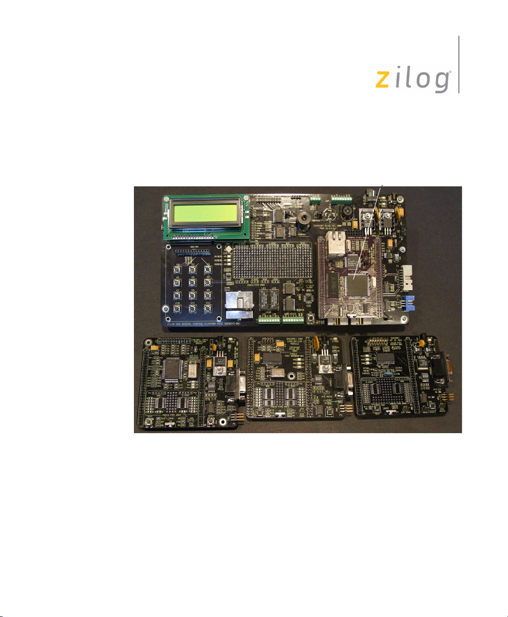
Figure 1 displays the MDS-GP application board with compatible
processor modules.
eZ80F91 Module
5
®
Z8 Encore! XP® 64K Series
Flash Microcontrollers Module
Z8 Encore! XP
Flash Microcontrollers Module
F0822 Series
Z8 Encore! XP®
Module
Figure 1. MDS-GP Board and Processor Modules
UM016905-1207 Introduction
Page 11

Kit Contents
The MDS-GP board development kit includes the following:
•
•
•
•
MDS General-Purpose Board Development Kit
User Manual
6
MDS-GP application board
Zilog® CD–ROM containing example projects and other
documentation
Quick Start Guide
10-pin to DB9 serial cable
UM016905-1207 Introduction
Page 12

MDS General-Purpose Board Development Kit
MDS-GP Board Features
Following sections describe features of the MDS-GP board:
•
MDS Interface
•
Power Supply Options
•
External Data Bus I/O
•
LCD Interface
•
Keypad
•
I2C Expanders
•
GPS and Wireless Data Options
User Manual
7
•
Software Selectable Serial Port Options
•
Board Jumper Settings
•
Relay/High Drive Outputs
•
Temperature Sensor
•
ADC Inputs
•
RS-485 I/O
•
Buzzer
•
Digital Compass Option
•
RAM and Flash Decode
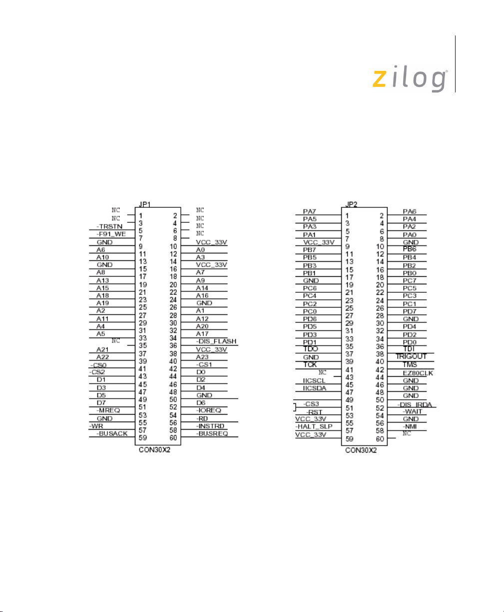
MDS Interface
The MDS interface consists of two 0.1 inch, 60 pin sockets, labeled JP1
and JP2, on the MDS-GP board. All MDS-compatible processor modules
include footprints for male headers to fit these sockets.
UM016905-1207 MDS-GP Board Features
Page 13
MDS General-Purpose Board Development Kit
User Manual
JP1 and JP2 reference signal names are based on the eZ80Acclaim!®
processor modules. When using another processor module, see corresponding section in Appendix—MDS-PM Board Pin Maps on page 33.
Figure 2 displays the reference signal names for the MDS headers.
8
Figure 2. JP1 and JP2 Reference Signal Names
UM016905-1207 MDS-GP Board Features
Page 14

MDS General-Purpose Board Development Kit
Power Supply Options
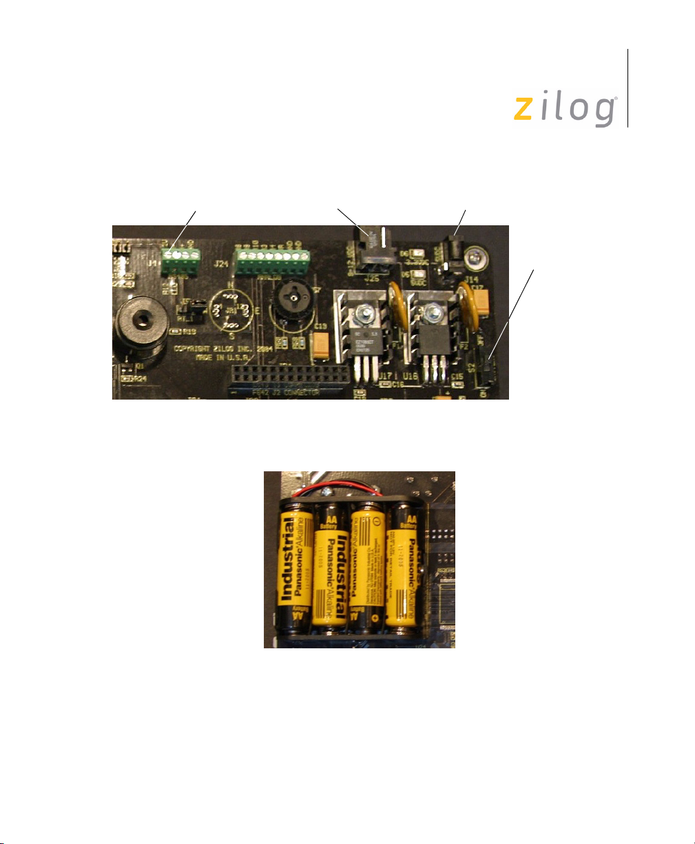
The MDS-GP board provides four different power input options (Figure 3
and Figure 4):
User Manual
9
Caution:
Caution:
Notes:
Connect only one power source at a time.
•
5 V DC into J14 — The 5 V power supply included with Zilog
MDS-PM development kits can be used for this input to power both
the MDS-GP board and the MDS processor module.
•
9 V to 12 V DC into J25 — The eZ80Acclaim!
with a 9 V DC power supply.
•
12 V DC into RS-485 connector, J4 — This connector provides another
means for supplying power to the board (Battery holder BT1 must be
empty).
•
4 AA cells in battery holder BT1 — Switch S2 present on the top right-
hand corner of the board turns the battery power source ON or OFF.
Ensure S2 is OFF or remove the batteries before connecting
another power source.
1. Do not use the DC input jack on the MDS-PM board when it is
plugged into the MDS-GP board. You must power the system with one
of the MDS-GP power supply inputs.
2. If your application is using the on-board relays, then you must
provide 9 V to 12 V DC into the MDS-GP board or change out the
relays to 5 V parts.
®
development kits ship
®
UM016905-1207 MDS-GP Board Features
Page 15
MDS General-Purpose Board Development Kit
User Manual
J4 (RS-485), 12 V DC J24, 9–12 V DC J14, 5 V DC
Battery Switch S2
(Use only one
power input)
Figure 3. Power Supply Connectors (Top Right Corner of MDS-GP Board)
10
Figure 4. BT1 Battery Pack (Located on Back of MDS-GP Board)
External Data Bus I/O
The MDS-GP board includes a 20 pin header (J7) that provides bus access
for any MDS processor module that supports an external data bus connec-
UM016905-1207 MDS-GP Board Features
Page 16
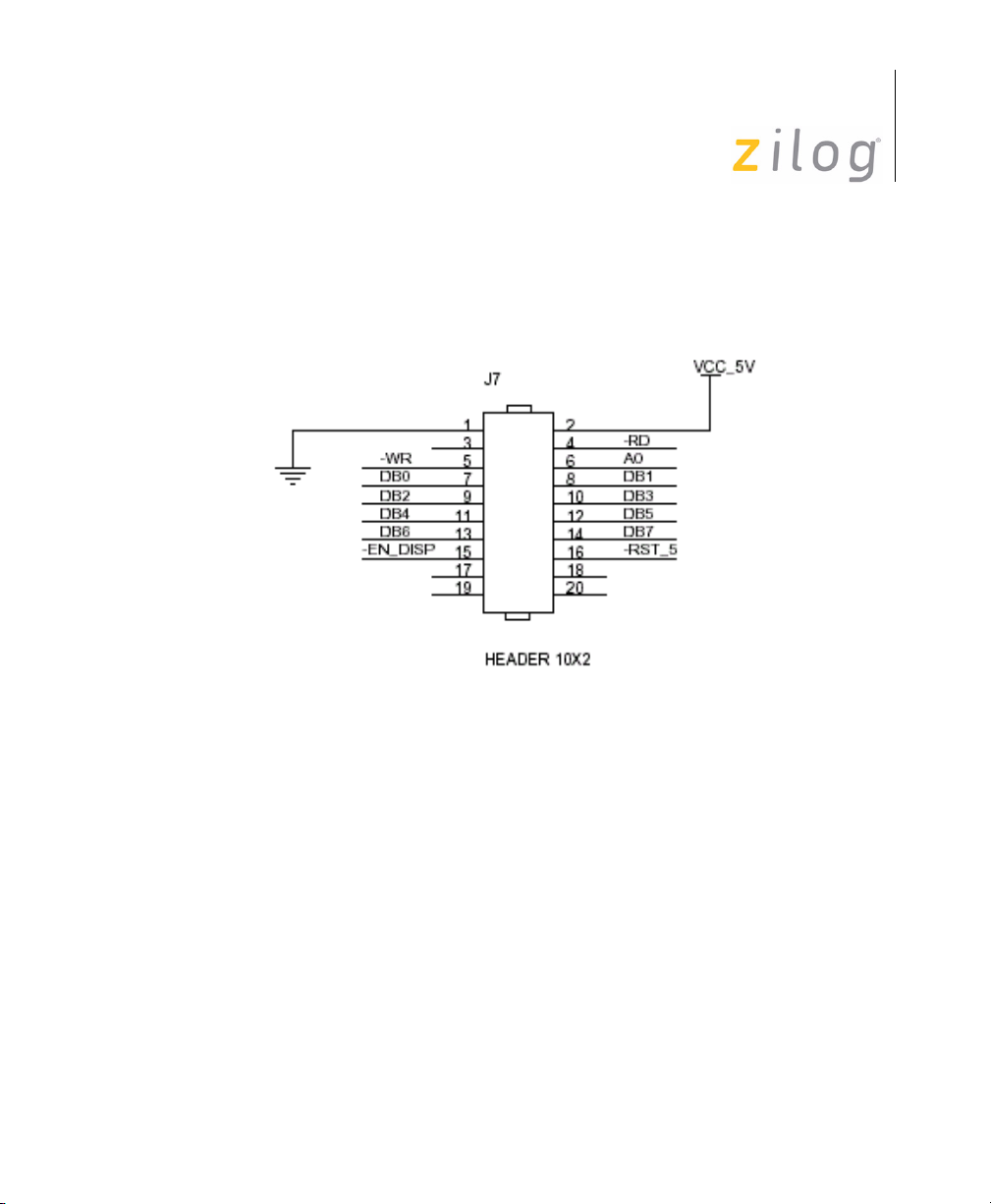
MDS General-Purpose Board Development Kit
User Manual
tion. This connector also provides 5 V DC power and a system reset line
(see Figure 5). The chip select control for this bus is generated from PAL
U26 and is programmed at the factory to decode address
Dxxxxh on CS2.
11
Figure 5. External Data Bus Header, J7
One application of this connector is to connect a higher-resolution graphic
display. The J7 header pin-out is same as CrystalFontz displays. For
example, you can connect a CrystalFontz 320 x 240 graphic LCD display
using just a ribbon cable. You can also power the display inverter for back
light control using the 5 V supply on this connector. The eZ80Acclaim!
®
software example includes routines that can be used to drive a
CrystalFontz display.
UM016905-1207 MDS-GP Board Features
Page 17

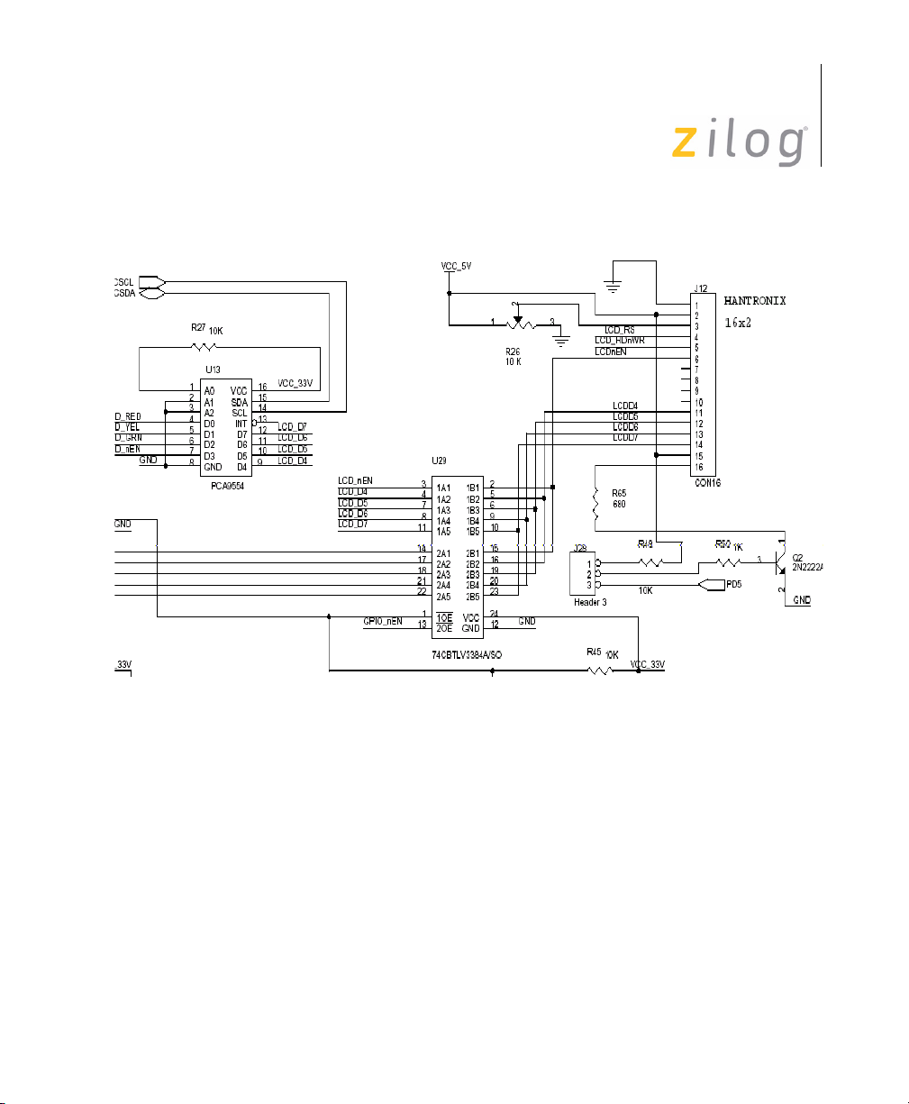
LCD Interface
Figure 6 displays the LCD interface on the MDS-GP board. It provides
the following two different interface options:
•
Four-bit parallel interface (using GPIO pins), controlled by LCD
enable, LCD RD/WR, and LCD register select signals.
•
I2C/I2C bus expander interface enabled by jumper J26
(see I
Note:
ZNEO
interfacing by four-bit parallel interface (GPIO pins). See
ZNEO
33.
LCD contrast can be adjusted using potentiometer R26. Software control
of the back light can be enabled using jumper J28. The default configuration drives the LCD in a four-bit mode using GPIO port pins of your MDS
processor module. For information on pins used, see Appendix—MDS-
PM Board Pin Maps on page 33.
MDS General-Purpose Board Development Kit
User Manual
2
C Expanders on page 16).
®
Z16F processor module requires minor changes for LCD
®
Z16F in Appendix—MDS-PM Board Pin Maps on page
12
UM016905-1207 MDS-GP Board Features
Page 18
MDS General-Purpose Board Development Kit
User Manual
13
Figure 6. LCD Interface
UM016905-1207 MDS-GP Board Features
Page 19

Keypad
Figure 7 displays the MDS-GP board with a 3 x 4 matrix keypad. The
keypad is controlled using GPIO port B. The four ROW pins have 10 K
pull-up resistors and are configured as inputs. The three COL pins are
configured as outputs. The software examples in this kit operate as
follows:
•
•
•
•
MDS General-Purpose Board Development Kit
User Manual
14
All ROW pins are configured as inputs, All COL pins are configured
as outputs and are initialized High.
In a interrupt routine, one COL pin is set Low and the ROW pins are
polled to check for a Low state.
If any ROW pin is polled Low, the key scan interrupt routine returns
the key pushed.
On each interrupt, a new COL pin is set Low. Three interrupts are
required to perform a full scan.
®
Note:
UM016905-1207 MDS-GP Board Features
ZNEO
keypad interfacing. See ZNEO® Z16F in Appendix—MDS-PM
Board Pin Maps on page 33.
Z16F processor module requires minor changes for
Page 20
MDS General-Purpose Board Development Kit
User Manual
15
Figure 7. Keypad Circuit
UM016905-1207 MDS-GP Board Features
Page 21

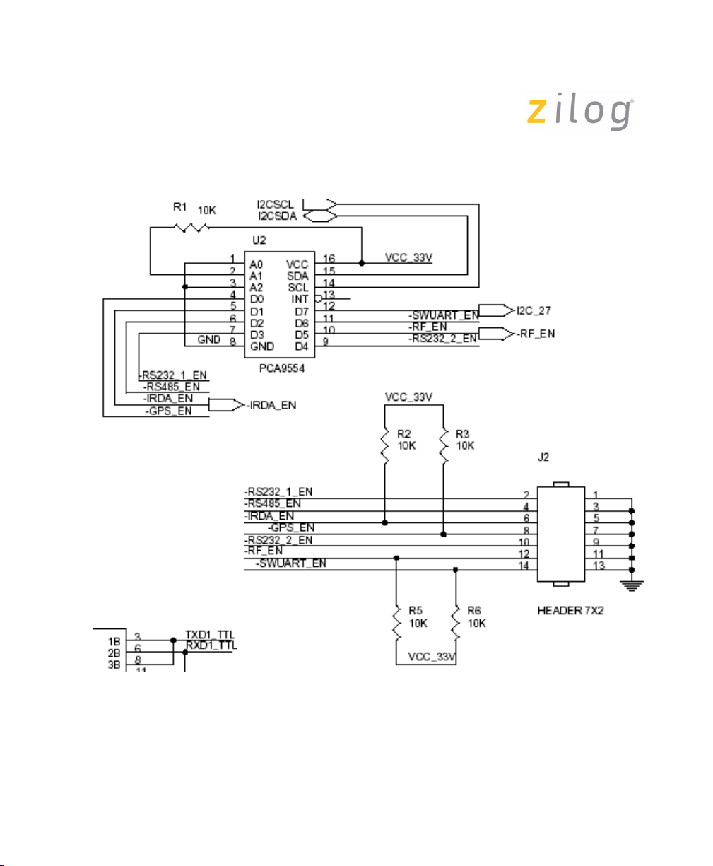
I2C Expanders
Three I2C bus expanders are included on the MDS-GP board: U2, U13,
and U19. The address of each device is hard-wired on the MDS-GP board
and is set to the functions and addresses as shown in Table 1.
MDS General-Purpose Board Development Kit
User Manual
16
Table 1. I
I2C Bus
Expander Address Function
U2 0100010 R/W Software serial port control jumpers
U13 0100001 R/W LCD four bit data, LCD enable pin
U19 0100000 R/W Relay/High drive outputs
2
C Bus Expanders
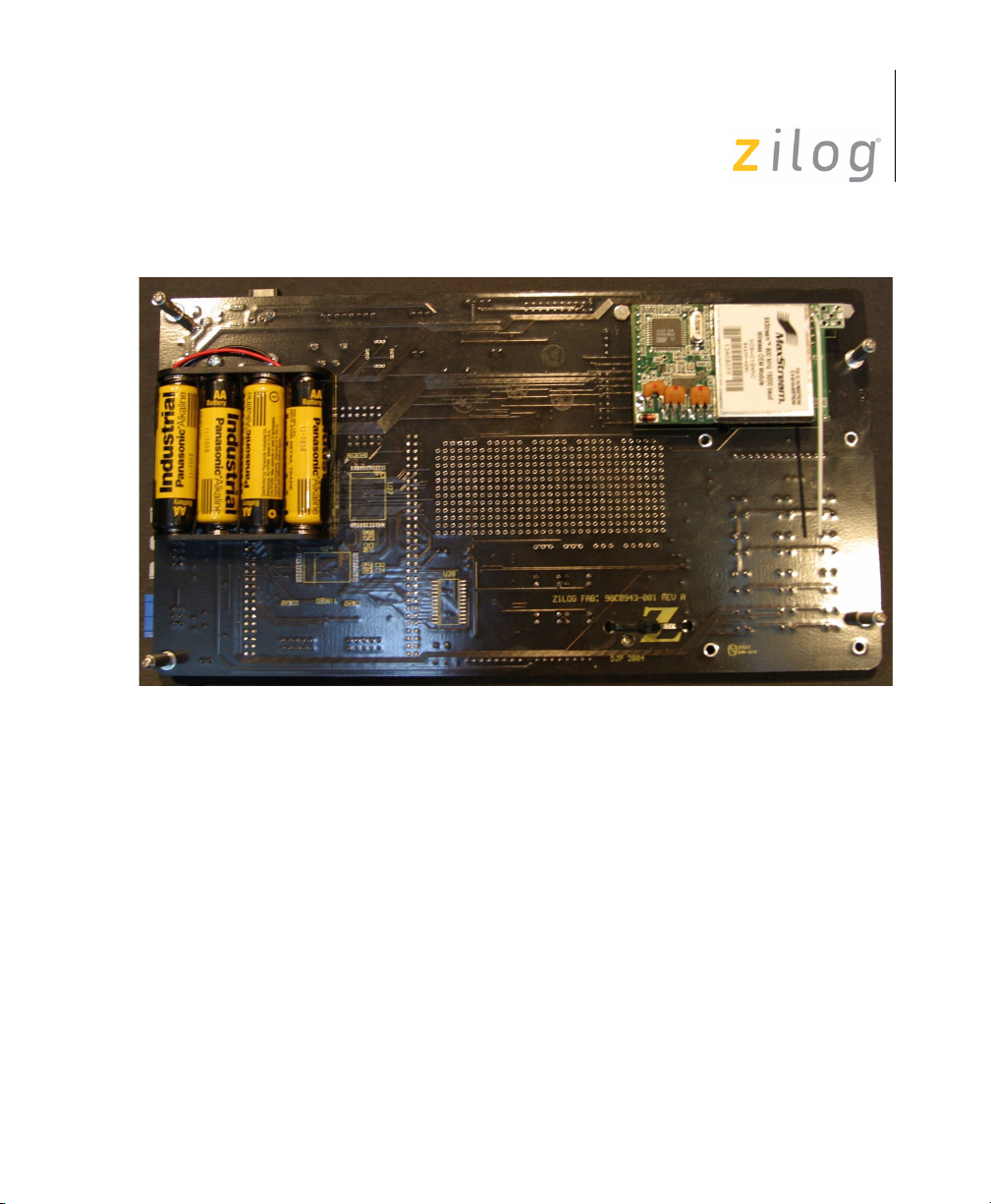
GPS and Wireless Data Options
The MDS-GP board supports plug-in options for adding wireless data and
GPS functions.
A two-way wireless module can be plugged into connectors J17 and J19
on the back of the MDS-GP board. The connector pinouts support the
maxstream 900 MHz and 2.4 GHz radio modules. For module details and
ordering information, visit www.maxstream.net
A trimble lassen SQ GPS module can be plugged into connector J15. For
module details and sales locations, visit www.trimble.com
The MDS-GP board is equipped with two holes for adding a wire-tie to
secure the module to the board. Figure 8 displays a maxstream wireless
module installed on the underside of the MDS-GP board.
and LED control
.
.
Note:
UM016905-1207 MDS-GP Board Features
These modules are not included in the MDS-GP board kit.
Page 22
MDS General-Purpose Board Development Kit
User Manual
17
Figure 8. Back of MDS-GP Board with Batteries and Wireless Option
Software Selectable Serial Port Options
Following serial port options are available on the MDS-GP board:
•
Two (four wire) 10 pin RS-232 ports on J1 (RS232-1) and J3
(RS232-2)
•
GPS can be configured to replace RS232-2
•
RF module can be configured to replace RS232-1
•
RS-485 port on J4 can be configured to replace RS232-1
•
IRDA port can be configured on MDS-PM to replace RS232-1
UM016905-1207 MDS-GP Board Features
Page 23

MDS General-Purpose Board Development Kit
User Manual
Only two different serial port options can be active at a time. The MDSGP board provides two ways to set active serial port options
(see Figure 9):
•
Jumper select options on J2 (seeTabl e 2 on page 20).
•
Use the I2C bus expander U2 to select options through software.
These options allow serial ports to be dynamically changed. You must
remove all J2 jumpers for software
selection to work.
18
UM016905-1207 MDS-GP Board Features
Page 24
MDS General-Purpose Board Development Kit
User Manual
19
Figure 9. U2 and J2 Serial Port Option Select Circuits
UM016905-1207 MDS-GP Board Features
Page 25

MDS General-Purpose Board Development Kit
Board Jumper Settings
Table 2 describes jumper set J2, which enables selected serial port
functions. You must not install any of these jumpers if software control is
used to enable serial port functions. The board is shipped with spare,
unconnected shunts on Pin 2 and Pin 10.
Table 2. Serial Port Control
Pins Factory Default Function
1, 2 OFF Enable RS232–1 on J1
3, 4 OFF Enable RS485 on J4 (replacing
5, 6 OFF Enable IRDA module (replacing
User Manual
20
RS232–1)
RS232–1)
7, 8 OFF Enable GPS on J15 (replacing
RS232–2)
9, 10 OFF Enable RS232– 2 on J3
11, 12 OFF Enable RF on J17 (replacing
RS232–1)
13, 14 OFF Enable software UART (replacing
RS232–2)
UM016905-1207 MDS-GP Board Features
Page 26

MDS General-Purpose Board Development Kit
Table 3 describes miscellaneous jumper settings on the MDS-GP board.
Table 3. Miscellaneous Jumper Settings
Jumper Symbol Name
User Manual
21
Factory
Default Function
J6 FL_WE Flash Write
Enable
OFF Install this jumper to enable writing
of the external flash memory boot
block on eZ80Acclaim!
®
processor
modules.
J5 RT-1 RS485 Term-
Res Enable
J8 DACK_EN Mot bus mode
Enable
OFF Install this jumper to enable the
RS-485 termination resistor.
OFF Install this jumper if running mot
bus mode when using the
eZ80Acclaim!
®
processor
modules.
J9 Disable
Flash
eZ80F91
External Flash
OFF Install this jumper to disable the
external flash memory on
eZ80Acclaim!
®
processor
modules.
J27 PWR_Sel Power Select 2, 3 This jumper selects the power
supply used for the relays and
high drive outputs available on
J20. Jumper pins 1, 2 for 5 V DC,
pins 2, 3 for 12 V DC.
UM016905-1207 MDS-GP Board Features
Page 27

MDS General-Purpose Board Development Kit
Table 3. Miscellaneous Jumper Settings (Continued)
Factory
Jumper Symbol Name
Default Function
User Manual
22
J26 LCD_Sel Data Control for
LCD
J28 BL LCD BackLight 1, 2 This jumper selects the LCD back
J29 ADC_POT POT Select ON This jumper connects the
OFF Install this jumper to select I2C
control of the LCD control pins.
light control. Jumper pins 2, 3 for
software control of backlight.
on-board potentiometer to one
ADC input.
Relay/High Drive Outputs
Figure 10 displays the two relays and six high-drive outputs included on
the MDS-GP board. By default, jumper J27 is set to route the 9 V to 12 V
DC power input to both the relays and the high-drive outputs. If 5 V DC is
used to power the MDS-GP board, then connect Pin 2 and Pin 3 on
jumper J27 to apply 5 V DC on the high-drive outputs.
The two relays installed on the board are 12 V DC types. These relays are
only supported when the 9 V to 12 V DC power supply input is used (see
Figure 10).
UM016905-1207 MDS-GP Board Features
Page 28

MDS General-Purpose Board Development Kit
User Manual
23
Figure 10. High-Drive and Relay Circuit
UM016905-1207 MDS-GP Board Features
Page 29

Temperature Sensor
MDS General-Purpose Board Development Kit
User Manual
24
Figure 11 displays the circuit for the I2C temperature sensor (U15)
2
included on the MDS-GP board. The I
C address for this device is set to
1001000 R/W.
The sensor’s over-temperature alarm output is shared with the keypad
ROW output. If the over-temperature alarm is used to interrupt the
system, check for a keypad ROW input before reading the temperature
sensor register.
Figure 11. I2C Temperature Sensor Circuit
ADC Inputs
Screw terminal block J24 allows you to bring in signals to drive some
ADC channels on a Z8 Encore! XP
UM016905-1207 MDS-GP Board Features
®
MDS-PM, ZNEO® MDS-PM, or
Page 30

MDS General-Purpose Board Development Kit
User Manual
some port pins on an eZ80Acclaim!® MDS-PM. The terminal block (see
Figure 12) also provides 5 V DC, 3.3 V DC, and ground terminals.
Ensure that jumper J29 is removed while using this terminal block as port
inputs. When J29 is installed, you can test the ADC using the on-board
potentiometer, R57, shown in Figure 13.
25
Figure 12. ADC Input Terminal Block
UM016905-1207 MDS-GP Board Features
Page 31

MDS General-Purpose Board Development Kit
User Manual
26
K
VCC_33V
R58
330
R57
2
1 3
R59
330
PA0
PA1
PA2
PA3
PB4_ANA4
HEADER 2
J29
1
2
PB4_ANA4
VCC_5V
SRAM, FLASH, ANALOG CONNECTORS
ZiLOG, Inc.
532 Race Street
San Jose, CA 95126
Figure 13. On-Board Potentiometer Circuit
J23
12
34
56
78
910
Header 5x2
PA0
PA1
PA2
PA3
VCC_33V
Terminal Block
J24
1
2
3
4
5
6
7
8
UM016905-1207 MDS-GP Board Features
Page 32

RS-485 I/O
Figure 14 displays the RS-485 port provided on screw terminal block J4.
This I/O can also provide power to the MDS-GP board through the 12 V
DC and GND lines, terminal 1 and terminal 4. An RS-485 termination
resistor can be enabled or disabled using jumper J5. The RS-485 driver
U8 is enabled through the RS-485_EN signal, which is controlled via
jumpers on J2 or by using the software I
in Software Selectable Serial Port Options on page 17.
MDS General-Purpose Board Development Kit
User Manual
2
C expander feature as described
27
Figure 14. RS-485 I/O Circuit
UM016905-1207 MDS-GP Board Features
Page 33

Buzzer
MDS General-Purpose Board Development Kit
User Manual
A 5 V DC buzzer is included on the MDS-GP board. For information on
pins used, see your module’s section in Appendix—MDS-PM Board Pin
Maps on page 33. Figure 15 displays the buzzer circuit using
eZ80Acclaim!
®
signal names.
28
Figure 15. Buzzer Circuit (eZ80Acclaim!® Pins)
Digital Compass Option
A footprint for an optional dinsmore 1490 digital compass is provided on
the MDS-GP board. This compass is a user-installed option, and 2525 not
included in the kit. For specifications and ordering information, visit
www.robsonco.com
UM016905-1207 MDS-GP Board Features
.
Page 34

MDS General-Purpose Board Development Kit
User Manual
29
Caution:
Due to possible electromagnetic interference (EMI) from the
circuitry surrounding the dinsmore 1490 digital compass,
®
Zilog
recommends mounting this device off-board using a
short ribbon cable.
RAM and Flash Decode
The MDS-GP board includes 512 KB fast SRAM, device U22. This
memory can only be used by MDS-PM board that supports an external
address/data bus.
The MDS-GP board also includes two footprints on the back of the board
for adding user- installed flash memory devices. Zilog
quality of added flash devices or their installation, so use these footprints
at your own risk.
Address decoding for the included SRAM, external I/O bus (see External
Data Bus I/O on page 10), and user- installed flash is factory programmed
by PAL U26, as shown in Tab le 4.
Table 4. PAL U26 Decode
Chip
Select Device
®
cannot control the
Decode
Address A23 A22 A21 A20
CS2 512 KB SRAM, U22 B0000h 1 0 1 1
External bus, J7 D0000h 1 1 0 1
CS0 User-installed Flash, U24 40000h 0 1 0 0
User-installed Flash, U27 50000h 0 1 0 1
UM016905-1207 MDS-GP Board Features
Page 35

MDS General-Purpose Board Development Kit
Troubleshooting
Overview
Perform the following steps before contacting Zilog® customer support to
submit a problem report:
1. Remove the MDS-GP board from the system; then, using your
processor module’s documentation, verify that your development system works correctly with the
MDS-GP board removed.
2. Use the instructions provided in the MDS General-Purpose Board
Quick Start Guide (QS0045) to reconnect the MDS-GP board and
return its jumpers to their factory default settings.
User Manual
23
3. Ensure that only one power supply is used which must be connected
to the MDS-GP board, not the processor module. Verify the power
supply input voltage with the system running.
4. Run the MDS-GP board example project appropriate for your
processor module.
If a hardware failure is suspected, contact a local Zilog representative for
assistance.
UM016905-1207 Troubleshooting
Page 36

MDS General-Purpose Board Development Kit
p
y
]D[
]
]
]
]PD[
]
]
]A[
]
p
[
]
]
]
]
]
]
[
]D[
]
[
]
User Manual
Schematics
MDS General Purpose Board
Figure 16 through Figure 23 provide schematic diagrams of the MDS-GP board.
5
D D
C C
B B
-IRDA_EN
-EN_DISP
-DIS_FLASH
GPIO_CON
-IRDA_EN
-EN_DISP
-DIS_FLASH
GPIO connectors
POWER
25
4
A[0:23
A[0:23
D[0:7
-WR
-CS2
-CS0
PA[0:7
PB[0:7
PC[0:7
I2CSDA
I2CSCL
-RST
-RST_5
0:7
-WR
-RD
-RD
-CS2
-CS0
PA[0:7
PB[0:7
PC[0:7
0:7
PD
0:7
I2CSDA
I2CSCL
-RST
-RST_5
PB
I2CSCL
RF_GPS
I2CSCL I2CSDA
I2C_27
-RF_EN
-RST_5
RF_GPS_COMPASS
PC4
PC6
PC7
0:7
PD5
PD6
PD7
PA4
PA5
PA6
PA7
GPS_TXD
I2C_27
RF_TXD
RF_RTS
-RF_EN
-RST_5
3
KEYPAD
PC4
PC6
PC7
PB[0:7
PD5
PD6
PD7
PA4
PA5
PA6
PA7
KEYPAD_ETC
GPS_RXD
GPS_PPS
I2CSDAI2CSCL
PD4
I2CSDAI2CSCL
RF_RXD
RF_CTS
North
East
South
West
I2CSDA
PD4
PA0
PA1
PA2
PA3
2
RAM_ADC
A
0:23
0:23
-CS0
-CS0
-CS2
-CS2
-RD
-RD
-WR
-WR
-RST -DIS_FLASH
PA0
PA0
PA1
PA1
PA2
PA2
PA3
PA3
SRAM
COMMS
PC0
PC2
PC2
PD0
PD0
PD2
I2CSCL I2CSDA
I2CSCL I2CSDA
GPS_RXD
GPS_PPS
RF_RXD
RF_CTS
PC5
PC5
COMMUNICATIONS
D[0:7
-EN_DISP
PC1
PC3
PD1
PD3
-IRDA_EN
GPS_TXD
I2C_27
-RF_EN
RF_TXD
RF_RTS
0:7
-EN_DISP
-DIS_FLASH-RST
PC1PC0
PC3
PD1
PD3PD2
-IRDA_EN
I2C_27
-RF_EN
SPARE
SPARE
1
arts
POWER
TOP
A A
5
4
3
2
ZiLOG, Inc.
532 Race Street
San Jose, CA 95126
Title
MDS General Pur
Size Document Number Rev
B
Date: Sheet of
, March 25, 2004
ose Platform.
96C0 943-001
18Thursda
1
B
Figure 16. MDS-GP Board Schematic (1 of 8)
UM016905-1207 Schematics
Page 37

MDS General-Purpose Board Development Kit
p
y
User Manual
5
U1
PC5
5
2
1A
1
1OE
5
2A
4
2OE
9
3A
10
3OE
12
4A
13
4OE
SN74CBT3125C
U4
2
1A
1
1OE
5
2A
4
2OE
9
3A
10
3OE
12
4A
13
4OE
SN74CBT3125C
PC0
PC1
VCC_33V
147
U7A
1 2
74LVC04/SO
U8
1
VCC
RO
2
B
RE
3
DE
A
4 5
DI GND
DS1487
VCC
GND
VCC
GND
8
7
6
1B
2B
3B
4B
1B
2B
3B
4B
VCC_5V
RF_RXD
RF_CTS
RF_TXD
RF_RTS
D D
GPS_RXD
GPS_PPS
GPS_TXD
C C
-SWUART_EN
B B
PD1
A A
PC5
PD0
3
6
8
11
14
7
3
6
8
11
14
7
I2CSCL
I2CSDA
VCC_5V
-RF_EN
-GPS_EN
VCC_5V
-RS485_EN
R9
10K
PD1
PD3
PD0
PD2
PC1
PC3
PC0
U5
2
1A
1
1OE
5
2A
4
2OE
9
3A
10
3OE
12
4A
13
4OE
SN74CBT3125C
VCC_33V
C11
0.1uF
VCC
GND
1B
2B
3B
4B
J5
RT_1
4
R1
-RS232_1_EN
-RS485_EN
-IRDA_EN
-GPS_EN
3
6
8
11
VCC_5V
14
7
1
2
4
10K
GND
TXD1_TTL
RXD1_TTL
R12
120
I2CSCL
I2CSDA
U2
1
A0
VCC
2
A1
SDA
3
A2
SCL
4
D0
INT
5
D1
D7
6
D2
D6
7
D3
D5
8 9
GND D4
PCA9554
-IRDA_EN
-RS232_1_EN
-RS485_EN
-IRDA_EN
-GPS_EN
-RS232_2_EN
-RF_EN
-SWUART_EN
VCC_12V_IN
J4
1
2
3
4
RS485
3
VCC_33V
16
15
14
13
12
11
10
-SWUART_EN
-RF_EN
-RS232_2_EN
VCC_33V
R2
10K
R5
10K
VCC_33V
I2C_27
-RF_EN
R3
10K
J2
2
1
4
3
6
5
8
7
10
9
12
11
14
13
HEADER 7X2
R6
10K
3
GND
GND
C7
0.1uF
C9
0.1uF
C2
0.1uF
C4
0.1uF
TxD0
RTS0
RxD0
CTS0
TXD1
RTS1
RxD1
CTS1
2
C1
VCC_33V
U3 MAX3222
1918
3
V+
VCCGND
7
V-
17
8
16
9
14
11
3
V+
7
V-
17
T1OUT
8
T2OUT
16
R1IN
9
R2IN
14
NC
11
NC
T1OUT
T2OUT
R1IN
R2IN
NC
NC
VCC_33V
1918
VCCGND
2
T1IN
T2IN
R1OUT
R2OUT
SHDN
U6 MAX3222
C1+
C1-
C2+
C2-
T1IN
T2IN
R1OUT
R2OUT
EN
SHDN
GND
GND
0.1uF
2
C1+
4
C1-
5
C2+
6
C2-
13
12
15
10
1
EN
20
R4
10K
C6
GND
0.1uF
2
4
5
6
13
12
15
10
1
20
R10
10K
ZiLOG, Inc.
532 Race Street
San Jose, CA 95126
Title
Size Document Number Rev
B
Date: Sheet of
C3
0.1uF
C5
0.1uF
VCC_33V
C8
0.1uF
C10
0.1uF
TXD1_TTL
RXD1_TTL
VCC_33V
MDS General Pur
, April 28, 2004
TXD1
RXD1
GND
ose Platform
96C0 943-001
1
RS232 - 1
J1
1
TxD0
3
RxD0
5
7
GND
9
CON10A
-RS232_1_EN
R7
10K
RS232 - 2
J3
1
3
5
7
9
CON10A
-RS232_2_EN
R11
10K
COMMUNICATIONS
1
PC2
PC3
2
CTS0
4
RTS0
6
8
10
PD0
PD2
PD1
PD3
2
CTS1
4
RTS1
6
8
10
28Wednesda
B
26
Figure 17. MDS-GP Board Schematic (2 of 8)
UM016905-1207 Schematics
Page 38

MDS General-Purpose Board Development Kit
p
y
]
]
]
]
]
]
User Manual
27
5
PB[0:7
D D
PD[0:7
PB0
PB1
PB2
PB3
PB4
PB5
PB6
PB7
PD0
PD1
PD2
PD3
PD4
PD5
PD6
PD7
A[0:23
C C
-RST
-RST
PA[0:7
PC[0:7
A0
A1
A2
A3
A4
A5
D[0:7
A6
A7
A8
A9
A10
A11
A12
A13
A14
A15
A16
A17
A18
A19
A20
A21
A22
A23
PA0
PA1
PA2
PA3
PA4
PA5
PA6
PA7
PC0
PC1
PC2
PC3
PC4
PC5
PC6
PC7
D0
D1
D2
D3
D4
D5
D6
D7
VCC_33V
VCC_33V
R13
147
TDI
TDO
TCK
VCC_33V
1
2
TC74LVC08
R14
10K
10K
P1
12
34
56
78
910
11 12
13 14
con 7x2
B B
14
U11A
GND
TC74LVT125
1
23
7
U12A
3
GND
R17
10K
TVCC_RESETn
A A
5
4
S1
1 3
-RESET
GND
TMS
PRSTn
TRIGOUT
4
J6
FL_WE
GND
1
2
12 11
3
JP2
PA7
12
PA5
34
PA3
56
PA1
78
VCC_33V
910
PB7
11 12
PB5
13 14
PB3
15 16
PB1
17 18
GND
19 20
PC6
21 22
PC4
23 24
PC2
25 26
27 28
PD6
29 30
PD5 D4
31 32
PD3
33 34
PD1
35 36
TDO
37 38
GND
39 40
TCK
41 42
NC
43 44
IICSCL
45 46
IICSDA
47 48
49 50
-CS3
-CS3
51 52
-RST
53 54
VCC_33V
55 56
-HALT_SLP -NMI
57 58
VCC_33V
59 60
CON30X2
-CS0
-CS2
-WR
VCC_5V
U11D
14
13
TC74LVT125
PA6
PA4
PA2
PA0
GND
PB6
PB4
PB2
PB0
PC7
PC5
PC3
PC1
PD7
GND
PD4
PD2
PD0
TDI
TRIGOUT
TMS
EZ80CLK
GND
GND
GND
-DIS_IRDA
-WAIT
GND
NC
JP1
NC
12
NC
34
-TRSTN
56
-F91_WE
78
GND
910
A6
11 12
A10
13 14
GND
15 16
A8
17 18
A13
19 20
21 22
A18
23 24
A19
25 26
A2
27 28
A11
29 30
A4
31 32
A5
33 34
NC
35 36
A21
37 38
A22
39 40
-CS0
41 42
-CS2
43 44
D1
45 46
D3
47 48
D5
49 50
D7
51 52
-MREQ
53 54
GND
55 56
-WR
57 58
-BUSACK
59 60
CON30X2
J11
VCC_33V
1
3
GND
5
R66
10K
ZDI INTERFACE
HEADER 3X2
NC
NC
NC
NC
VCC_33V
A0
A3
VCC_33V
A7
A9
A14A15
A16
GND
A1
A12
A20
A17
-DIS_FLASH
VCC_33V
A23
-CS1
D0
D2
D4
GND
D6
-IOREQ
-RD
-INSTRD
-BUSREQ
2
4
6
-RESET
TCK
TDI
VCC_33V
U7F
147
74LVC04/SO
1312
GND
R16 10K
1
2
J9
DIS_FL
-RD
VCC_33V
-DIS_FLASH
-RST_5
7
3
2
-IRDA_EN
2
1
VCC_5V
C12
CAP_NP
2010
D0
D1
D2PC0
D3
D5
D6
D7
74ACT245
-WR
DB0
DB2
DB4
DB6
-EN_DISP
U9
18
B0
17
B1
16
B2
15
B3
14
B4
13
B5
12
B6
11
B7
1
3
5
7
9
11
13
15
17
19
DB0
2
A0
DB1
3
VCCGND
A1
DB2
4
A2
DB3
5
A3
DB4
6
A4
DB5
7
A5
DB6
8
A6
DB7
9
A7
-WR
1
DIR
19
OE
-RD
A0
DB1
DB3
DB5
DB7
-RST_5
VCC_5V
J7
2
4
6
8
10
12
14
16
18
20
HEADER 10X2
-WAIT
-EN_DISP
J8
1
-DACK_EN
2
VCC_5V
DO NOT POPULATE R15 and R18
R15
4.7K
OFFBOARD
IICSDA
IICSCL
ose Platform
1
2
3
4
1
I2CSDA
I2CSCL
R18
4.7K
IF R15 and R18 ARE POPULATED R29 AND R30 MUST BE REMOVED
ZiLOG, Inc.
532 Race Street
San Jose, CA 95126
Title
Size Document Number Rev
Date: Sheet of
MDS System interface, I/O
MDS General Pur
B
, March 25, 2004
96C0 943-001
J10
1
2
3
4
-EN_DISP
I2C_CON
B
38Thursda
Figure 18. MDS-GP Board Schematic (3 of 8)
UM016905-1207 Schematics
Page 39

MDS General-Purpose Board Development Kit
p
y
[
]
]
User Manual
5
K1
1 3
SW_PB
D D
K4
1 3
SW_PB
K7
1 3
SW_PB
C C
B B
A A
PB[0:7
1 3
COL0
COL1
COL2
J13
N
M
K
H
G
E
D
C
B
A
HEADER 13
F
L
J
K10
SW_PB
1
2
3
4
5
6
7
8
9
10
11
12
13
PB
0:7
K2
1 3
SW_PB
K5
1 3
SW_PB
K8
1 3
SW_PB
K11
1 3
SW_PB
PB0 LCD_RDnWR
COL0
PB1
COL1
PB2
COL2
PB3
ROW0
PB4
ROW1
PB5
ROW2
PB6
ROW3
I2CSDA
I2CSCL
4.7K
R29
PB7
5
K3
1 3
SW_PB
K6
1 3
SW_PB
K9
1 3
SW_PB
K12
1 3
SW_PB
VCC_33V
R30
4.7K
U15
1
SDA
2
GND
3 4
SCL OT
MAX6625P
VCC
ADD
4
VCC_33V
R20
10K
ROW0
VCC_33V
R23
10K
PC7
HEADER 2
R33
10K
J26
PD7
PA4
PA5
PA6
PA7
ROW0
ROW1
ROW2
ROW3
R34
10K
PC6
1
2
VCC_33V
I2CSCL
I2CSDA
LED_RED
LED_YEL
LED_GRN
LCD_nEN
GND
1
2
3
4
5
6
11
12
PC4
PD6
ROW1
VCC_33V
R25
10K
ROW2
VCC_33V
R28
10K
ROW3
R31
4.7K
R32
10K
6
5
4
3
PC7
PC6 LCD_RS
GND
U14
147
8
74LV30/SO
PD6
3
R24
BUZZER
1K
R27
10K
U13
1
A0
VCC
2
A1
SDA
3
A2
SCL
4
D0
INT
5
D1
D7
6
D2
D6
7
D3
D5
8 9
GND D4
PCA9554
147
U7C
5 6
74LVC04/SO
J30
1
2
3
Header 3
16
15
14
13
12
11
10
3
VCC_33V
LCD_D7
LCD_D6
LCD_D5
LCD_D4
VCC_5V
2
BZ1
Buzzer
1
1
Q1
2N2222A
2
LCD_nEN
LCD_D4
LCD_D5
LCD_D6
LCD_D7
14
5 6
7
VCC_33V
R19
330
4
GPIO_nEN
U11B
TC74LVT125
2
VCC_33V
D2
LED_YEL
LCD_RDnWR
LCDnEN
J28
1
2
3
Header 3
R45
U7B
74LVC04/SO
, April 28, 2004
R56
680
LCD_RS
LCDD4
LCDD5
LCDD6
LCDD7
R65
10K
D3
LED_GRN
56.2
R48
10K
VCC_33V
GPIO_nEN
ose Platform
96C0 943-001
R22
R21
680
680
21
D1
LED_RED
LED_RED
LED_YEL
LED_GRN
VCC_5V
2
1 3
R26
10 K
U29
3
4
7
8
11
14
17
18
21
22
1
2
1B1
1A1
5
1B2
1A2
6
1B3
1A3
9
1B4
1A4
10
1B5
1A5
15
2B1
2A1
16
2B2
2A2
19
2B3
2A3
20
2B4
2A4
23
2B5
2A5
24
VCC
1OE
1213
GND2OE
74CBTLV3384A/SO
GND
147
3 4
PD4
R44
BUZZER, KEYPAD, LCD, I2C TEMP. SENSOR
10K
2
ZiLOG, Inc.
532 Race Street
San Jose, CA 95126
Title
MDS General Pur
Size Document Number Rev
B
Date: Sheet of
1
J12
1
2
3
4
5
6
7
8
9
10
11
12
13
14
15
16
CON16
1
HANTRONIX
16x2
R50
1K
PD5
48Wednesda
1
Q2
3
2N2222A
2
GND
B
28
Figure 19. MDS-GP Board Schematic (4 of 8)
UM016905-1207 Schematics
Page 40

MDS General-Purpose Board Development Kit
p
y
User Manual
29
5
VCC_12V_IN
9-12 VOLTS, 1000mA
J14
5VDC IN
J25
12VDC IN
2
3
1
2
3
1
F2
RXE160
BT1
BATTERY
GND
C20
0.1uF
5
6
4
3
F1
RXE160
C16
0.1uF
U18
IN
IN
EN
GND
TPS7250
D D
C C
B B
VCC_12V
C15
0.1
C17
+
22uF
SENSE
OUT
OUT
C21
+
10uF
4
1 3
2
PG
1
7
8
U16
LM7805C/TO220/0.5A
IN OUT
GND
2
BAT ON
R37
200K
U17
3 2
VIN VOUT
GND
1
S2
C13
0.1
LT1086-3.3/TO220
VCC_33V
3
VCC_5V
R35
680
C14
22uF
+
21
D5
AMBER
5 OK
VCC_33V
C19
22uF
21
3.3 OK
R36
680
D6
LED
GRN
C18
0.1uF
+
2
1
, March 25, 2004
POWER
ose Platform
96C0943-001 B
58Thursda
1
A A
5
4
3
2
ZiLOG, Inc.
532 Race Street
San Jose, CA 95126
Title
MDS General Pur
Size Document Number Rev
B
Date: Sheet of
Figure 20. MDS-GP Board Schematic (5 of 8)
UM016905-1207 Schematics
Page 41

MDS General-Purpose Board Development Kit
p
y
g
y
y
User Manual
5
D D
J16
1
2
3
4
5
6
7
8
HEADER 8
I2CSCL
I2CSDA
C C
RELAY1
RELAY2
HI-DRIVE1
HI-DRIVE2
B B
A A
U19
1
A0
VCC
2
A1
SDA
3
A2
SCL
4
D0
INT
5
D1
D7
6
D2
D6
7
D3
D5
8 9
GND D4
PCA9554
J20
HEADER 8
5
HI-DRIVE6
HI-DRIVE5
HI-DRIVE4
HI-DRIVE3
GND
VCC_33V
C22
0.001uF
16
15
14
13
12
11
10
1
2
3
4
5
6
7
8
7
8
7
8
RELAY1
RELAY2
HI-DRIVE1
HI-DRIVE2
HI-DRIVE3
HI-DRIVE4
HI-DRIVE5
HI-DRIVE6
4
LS1
Reed Rela
LS2
Reed Rela
4
1
14
2
6
1
14
2
6
U20
1
IN1
OUT1
2
IN2
OUT2
3
IN3
OUT3
4
IN4
OUT4
5
IN5
OUT5
6
IN6
OUT6
7
IN7
OUT7
8
IN8
OUT8
9 10
GND COM
AIC2803CN
3
VCC_12V
J27
1
2
3
Header 3
18
17
16
15
14
13
12
11
VCC_5V
GPS_RXD
GPS_TXD GPS_PPS
RF_CTS
-RF_EN
RF_RXD
RF_TXD
RF_RTS
-RST_5
I2C_27
R38
100
VCC_5V
123
JR1
N1N2N3
4
5
6
W1
W2
W3
ital Compass
Di
S1S2S3
789
12
E3
11
E2
10
E1
RF, GPS, RELAYS, HIGH DRIVE OUTPUTS
3
RFRX
2
GPS_RXD
GPS_TXD
VCC_33V
J18
HEADER 4
21
D8
LED
R54
100
DO NOT POPULATE
2
1
GPS_CONN
J15
2
1
4
3
6
5
8
7
C40
+
C39
22uF
0.1uF
-TTL_CTS
TTL-RXD
TTL-TXD
-TTL-RTS
1
2
3
4
VCC_5V
21
D7
LED
RFTX
R55
100
ZiLOG, Inc.
532 Race Street
San Jose, CA 95126
Title
Size Document Number Rev
B
Date: Sheet of
VCC_5V
R39
R40
10K
10K
MDS General Pur
, April 21, 2004
RXLED
-TX/PWR
-CONFIG
VCC_5V
GND
R41
10K
ose Platform
96C0 943-001
R42
10K
GPS_PPS
1
2
3
4
5
6
7
8
9
10
11
1
J17
HEADER 11
J19
1
2
3
4
HEADER 4
NORTH
EAST
SOUTH
WEST
68Wednesda
B
30
Figure 21. MDS-GP Board Schematic (6 of 8)
UM016905-1207 Schematics
Page 42

MDS General-Purpose Board Development Kit
p
y
User Manual
31
5
D D
C C
R51
0
B B
R52
0
4
147
U7D
9 8
74LVC04/SO
147
U7E
11 10
74LVC04/SO
VCC_33V
3
U11C
14
10
R47
10K
9 8
7
TC74LVT125
2
U12B
R43
0
R46
0
R49
0
147
4
5
9
10
12
13
TC74LVC08
6
U12C
147
TC74LVC08
8
U12D
147
TC74LVC08
11
1
SPARES
A A
5
4
3
2
ZiLOG, Inc.
532 Race Street
San Jose, CA 95126
Title
MDS General Pur
Size Document Number Rev
B
Date: Sheet of
, March 23, 2004
ose Platform
99C0 943-001 B
78Tuesda
1
Figure 22. MDS-GP Board Schematic (7 of 8)
UM016905-1207 Schematics
Page 43

MDS General-Purpose Board Development Kit
p
y
]
]
User Manual
32
5
A[0:23
D D
D[0:7
C C
-RST
-CS2
-RD
-WR
-EN_DISP
B B
-CS0
-DIS_FLASH
A A
A20
A21
-CS0
-CS2
A22
A23
A0
A1
A2
A3
A4
A5
A6
A7
A8
A9
A10
A11
A12
A13
A14
A15
A16
A17
A18
A19
A20
A21
A22
A23
D0
D1
D2
D3
D4
D5
D6
D7
-CS2
A23
A22
A21
A20
5
A0
A1
A2
A3
A4
A5
A6
A7
A8
A9
A10
A11
A12
A13
A14
A15
A16
A17
A18
A19
A20
A21
A22
A23
U26
2
I
3
I
4
I
5
I
6
I
7
I
8
I
9
I
11
I/OE
1
I/CLK
16LV8
R8
10K
R60
10K
R61
10K
R62
10K
R63
10K
R64
10K
U21
2
1A1
1Y1
4
1A2
1Y2
6
1A3
1Y3
1Y41A4
11
2A1
2Y1
13
2A2
2Y2
15
2A3
2Y3
17
2A4
2Y4
1 20
1OE
VCC
19
GND
2OE
74LVC241/SO
U23
2
1A1
1Y1
4
1A2
1Y2
6
1A3
1Y3
1Y41A4
11
2A1
2Y1
13
2A2
2Y2
15
2A3
2Y3
17
2A4
2Y4
1 20
1OE
VCC
19
2OE
GND
74LVC241/SO
U25
2
1A1
1Y1
4
1A2
1Y2
6
1A3
1Y3
1Y41A4
11
2A1
2Y1
13
2A2
2Y2
15
2A3
2Y3
17
2A4
2Y4
1 20
1OE
VCC
19
GND
2OE
74LVC241/SO
12
I/O
13
I/O
14
I/O
15
I/O
16
I/O
17
I/O
18
I/O
19
I/O
VCC_33V
20
VCC
10
GND
VCC_33V
18
16
14
128
9
7
5
3
10
GND
18
16
14
128
9
7
5
3
10
18
16
14
128
9
7
5
3
10
-EN_DRV
-SRAM_EN
C35
0.001uF
BA0
BA1
BA2
BA3
BA4
BA5
BA6
BA7
BA8
BA9
BA10
BA11
BA12
BA13
BA14
BA15
GND
BA16
BA17
BA18
BA19
BA20
VCC_33V
GND
VCC_33V
C23
0.001uF
VCC_33V
C29
0.001uF
C31
0.001uF
VCC_33V
4
C30
0.1uF
C32
0.1uF
4
C24
0.1uF
3
BA0
BA1
BA2
BA4
BA5
BA6
BA7 D7
BA8
BA9
BA10
BA11
BA12
BA13
BA14
BA15
BA16
BA17
C34
0.1uF
-EN_DRV
BA18
-SRAM_EN
-WR
-RD
F_D0
F_D1
F_D2
F_D3
F_D4
F_D5
F_D6
F_D7
U24 AND U27 ARE ON THE SOLDER SIDE OF THE BOARD
U24
BA0
21
A0
A1
A2
A3
A4
A5
A6
A7
A8
A9
A10
A11
A12
A13
A14
A15
A16
A17
A18
A19
RESET
OE
WE
CE
D0
D1
D2
D3
D4
D5
D6
D7
D8
D9
D10
D11
D12
D13
D14
NC
NC
VCC
GND
GND
D0
D1
D2
D3
D4
D5
D6
D7
NC
NC
NC
RY/BY
VCC
VCC
GND
GND
Am29LV008B
29
31
33
35
38
40
42
44
30
32
34
36
39
41
43
45
10
13
15
37
27
46
BA1
20
BA2
19
BA3
18
BA4
17
BA5
16
BA6
15
BA7
14
BA8
8
BA9
7
BA10
36
BA11
6
BA12
5
BA13
4
BA14
3
BA15
2
BA16
1
BA17
40
BA18
13
BA19
37
-RST
10
-RD
24
-WR
9
22
U27
BA1
25
A0
BA2
24
A1
BA3
23
A2
BA4
22
A3
BA5
21
A4
BA6
20
A5
BA7
19
A6
BA8
18
A7
BA9
8
A8
BA10
7
A9
BA11
6
A10
BA12
5
A11
BA13
4
A12
BA14
3
A13
BA15
2
A14
BA16
1
A15
BA17
48
A16
BA18
17
A17
BA19
16
A18
BA20
9
-WR
12
14
28
26
11
47
A19
RESET
VPP
OE
CE
WE
BYTE
AT49BV162A
-RST
10K
R53
-RD
D15/A-1
RY/BY
3
25
26
27
28
32
33
34
35
11
38
29
12
31
30
39
23
F_D0
F_D1
F_D2
F_D3
F_D4
F_D5
F_D6
F_D7
BA0
VCC_33V
C36
0.001uF
F_D0
F_D1
F_D2
F_D3
F_D4
F_D5
F_D6
F_D7
VCC_33V
C33
0.001uF
C37
0.1uF
VCC_33V
1
2
3
4
5
14
15
16
17
18
20
21
22
23
24
32
33
34
35
19
36
6
13
31
11
14
17
18
21
22
5K
2
U22
A0
A1
A2
A3
A4
A5
A6
A7
A8
A9
A10
A11
A12
A13
A14
A15
A16
A17
A18
NC
VDD0
NC
VDD1
CE
WE
OE
VSS0
VSS1
AS7C34096
U28
3
1B1
1A1
4
1B2
1A2
7
1B3
1A3
8
1B4
1A4
1B5
1A5
2B1
2A1
2B2
2A2
2B3
2A3
2B4
2A4
2B5
2A5
VCC
1
1OE
GND2OE
74CBTLV3384/SO
VCC_33V
R58
330
R57
2
1 3
R59
330
2
D0
7
D0
D1
8
D1
D2
11
D2
D3BA3
12
D3
D4
25
D4
D5
26
D5
D6
29
D6
30
D7
9
27
C25
0.001uF
10
28
D0
2
D1
5
D2
6
D3
9
D4
10
D5
15
D6
16
D7
19
20
GND
23
VCC_33V
24
1213
GND
0.001uF
HEADER 2
J29
1
2
SRAM, FLASH, ANALOG CONNECTORS
ZiLOG, Inc.
532 Race Street
San Jose, CA 95126
Title
Size Document Number Rev
B
Date: Sheet of
VCC_33V
C27
C26
0.001uF
0.1uF
GND
PH0_ANA8
PH1_ANA9
PB4_ANA4
PB5_ANA5
PB6_ANA6
PB7_ANA7
PH2_ANA10
C38
PH3_ANA11
PA0
PA1
PA2
PA3
PB4_ANA4
MDS General Pur
96C0 943-001 B
, March 25, 2004
C28
0.1uF
PA0
PA1
PA3
PA2
PB4_ANA4
VCC_5V
ose Platform
1
J21
25
23
21
19
17
15
13
11
9
7
5
3
1
HEADER 13X2
J23
12
34
56
78
910
Header 5x2
VCC_33V
88Thursda
1
PA0
PA1
PA2
PA3
26
24
22
20
18
16
14
12
10
8
6
4
2
J24
1
2
3
4
5
6
7
8
Terminal Block
Figure 23. MDS-GP Board Schematic (8 of 8)
UM016905-1207 Schematics
Page 44

MDS General-Purpose Board Development Kit
User Manual
Appendix—MDS-PM Board Pin
Maps
Signals on MDS-GP connectors J1 and J2 map to processor module signal
names differently for different modules.
Following sections list MDS-GP interface signals with the corresponding
processor module signals:
•
eZ80Acclaim!® MCUs on page 34
•
Z8 Encore! XP® 64K Series Flash Microcontrollers on page 39
•
Z8 Encore! XP® F0822 Series Flash Microcontrollers on page 45
•
Z8 Encore! XP® MCUs on page 56
33
•
ZNEO® Z16F Series MCUs on page 63
Current pin maps are also included in the sample project folders on the
MDS-GP CD-ROM.
UM016905-1207 Appendix—MDS-PM Board Pin Maps
Page 45

eZ80Acclaim!® MCUs
Spare Pins
PD6 (DCD input) and PC4 (DTR output).
LCD Control
The LCD has two different modes of operation, 4-bit bus mode and I2C
drive mode, controlled by jumper J26:
•
J26 OFF, LCD bus mode enabled
•
J26 ON, LCD I2C drive mode enabled
Bus Mode LCD Control
•
LCD_EN—PD7 (eZ80F91 MCU alternate function: RI input)
MDS General-Purpose Board Development Kit
User Manual
34
•
LCD_RS—PC6 (eZ80F91 MCU alternate function: DCD input)
•
LCD_RW—PB0
•
LCD_D4—PA4
•
LCD_D5—PA5
•
LCD_D6—PA6
•
LCD_D7—PA7
2
C Drive Mode LCD Control
I
2
U13 I
C bus address: 0100001 R/W
•
LCD_EN—I2C bus expander address 1—D3
•
LCD_RS—PC6 (eZ80F91 MCU alternate function: DCD input)
•
LCD_RW—PB0
•
LCD_D4—I2C bus expander address 1—D4
UM016905-1207 Appendix—MDS-PM Board Pin Maps
Page 46

•
LCD_D5—I2C bus expander address 1—D5
•
LCD_D6—I2C bus expander address 1—D6
•
LCD_D7—I2C bus expander address 1—D7
•
LCD BackLight—PD5
Buzzer Control
BUZZER—PC7 (eZ80F91 MCU alternate function: RI input)
KeyPad Control
•
COL0—PB1
•
COL1—PB2
•
COL2—PB3
MDS General-Purpose Board Development Kit
User Manual
35
•
ROW0—PB4
•
ROW1—PB5
•
ROW2—PB6
•
ROW3—PB7
•
IRQ_KEYPAD_TEMP—PD4 (eZ80F91 MCU alternate function:
DTR output)
LED Control
U13 I2C bus address: 0100001 R/W.
•
RED_LED—I2C bus expander address 1—D0
•
YELLOW_LED—I2C bus expander address 1—D1
•
GREEN_LED—I2C bus expander address 1—D2
UM016905-1207 Appendix—MDS-PM Board Pin Maps
Page 47

Serial Port Control
Jumper J2 Signals
Enable only one serial port function per interface (COM1 or COM2).
•
RS232_COM1_ENABLE—J2 pins 1, 2
•
RS485_COM1_ENABLED—J2 pins 3, 4
•
IrDA ENABLE (COM1)—J2 pins 5, 6
•
RS232_GPS_COM2_ENABLED—J2 pins 7, 8
•
RS232_COM2_ENABLE—J2 pins 9, 10
•
RS232_RF_COM1_ENABLED—J2 pins 11, 12
•
SOFTWARE_UART_COM1_ENABLED—J2 pins 13, 14
2
C Bus Expander U2 Signals for Serial Port Control
I
U2 is an I
signals on jumper J2. If the U2 I
jumpers are removed from J2. U2 powers up with all pins in input mode.
The U2 bus expander I
2
C bus expander that can be used via software to control the
MDS General-Purpose Board Development Kit
User Manual
2
C expander is to be used, ensure all
2
C address is 0100010 R/W.
36
•
GPS_ENABLE—D0 = 0
•
IrDA ENABLE—D1 = 0
•
RS485 ENABLE—D2 = 0
•
RS232_COM1_ENABLE—D3 = 0
•
RS232_COM2_ENABLE—D4 = 0
•
RF_ENABLE—D5 = 0
•
SW_UART_ENABLE—D6 = 0
•
Spare—D7
UM016905-1207 Appendix—MDS-PM Board Pin Maps
Page 48

MDS General-Purpose Board Development Kit
User Manual
RS232-1 Signals
Enabled by jumper on J2 pins 1, 2, or by U2 pin D3. Uses COM1.
When enabled, disables RS-485, IrDA, and RF.
•
TXD—PD0_TXD0
•
RXD—PD1_RXD0
•
CTS—PD3_CTS0
•
RTS—PD2
RS232-2 Signals
Enabled by jumper on J2 pins 9, 10, or by U2 pin D4. Uses COM2.
When enabled,
disables GPS and Software UART.
•
TXD—PC0_TXD1
37
•
RXD—PC1_RXD1
•
CTS—PC3_CTS1
•
RTS—PC2 _RTS1
IrDA Module Signals
Enabled by jumper on J2 pins 5, 6, or by U2 pin D1. Uses COM1.
When enabled, disables RS232-1, RS485, and RF.
•
TXD—PD0_TXD0
•
RXD—PD1_RXD0
•
Not used—PD3
•
IrDA_SD—PD2
UM016905-1207 Appendix—MDS-PM Board Pin Maps
Page 49

MDS General-Purpose Board Development Kit
User Manual
Wireless (RF) Module Signals
Enabled by jumper on J2 pins 11, 12, or by U2 pin D5. Uses COM1.
When enabled, disables RS232-1, RS485, and IrDA.
•
RF_TXD—PD0_TXD0
•
RF_RXD—PD1_RXD0
•
RF_CTS0—PD3_CTS0
•
RF_RTS0—PD2_RTS0
•
RF_RESET—System Reset
GPS Module Signals
Enabled by jumper on J2 pins 7, 8, or by U2 pin D0. Uses COM1.
Uses COM2. When enabled, disables RS232-2 and Software UART.
38
•
GPS_TXD—PC0_TXD1
•
GPS_RXD—PC1_RXD1
•
GPS_PPS—PC3_CTS1 (Input)
•
Not used—PC2
RS485 Port Signals
Enabled by jumper on J2 pins 3, 4, or by U2 pin D2. Uses COM1.
When enabled, disables RS232-1, IrDA, and RF.
•
RS485_TXD—PD0_TXD0
•
RS485_RXD—PD1_RXD0
•
Not used—PD3
•
RS485_OE—PC5 (eZ80F91 MCU alternate function: DSR input)
UM016905-1207 Appendix—MDS-PM Board Pin Maps
Page 50

MDS General-Purpose Board Development Kit
Software UART Signals
Enabled by jumper on J2 pins 13, 14, or by U2 pin D6. When enabled,
disable RS232-2 and GPS.
•
SU_TXD—I2C_SCL
(This function is not available for eZ80F91 Module)
•
SU_RXD—I2C_SDA
(This function is not available for eZ80F91 Module)
•
CTS—PC3_CTS1
•
RTS—PC2_RTS1
I2C Temperature Sensor U15, Maxim MAX6625
U15 I2C address: 1001000 R/W.
User Manual
39
•
IRQ_KEYPAD_TEMP—PD4 (eZ80F91 MCU alternate function:
DTR output)
I2C High Drive/Relay Control
I2C address: 0100000 R/W.
•
RELAY1—D0
•
RELAY2—D1
•
HD1-J20-1—D2
•
HD2-J20-2—D3
•
HD3-J20-3—D4
•
HD4-J20-4—D5
•
HD6-J20-5—D6
UM016905-1207 Appendix—MDS-PM Board Pin Maps
Page 51

Digital Compass
Compass is not included.
•
NORTH—PA0 J21-21, J24-1
(eZ80F91 MCU alternate function: PWM0 output. Compare0 output)
•
EAST—PA1 J21-19, J24-2
(eZ80F91 MCU alternate function: PWM1 output. Compare1 output)
•
SOUTH—PA2 J21-7, J24-3
(eZ80F91 MCU alternate function: PWM2 output. Compare2 output)
•
WEST—PA3 J21-9, J24-4
(eZ80F91 MCU alternate function: PWM3 output. Compare3 output)
MDS General-Purpose Board Development Kit
User Manual
40
UM016905-1207 Appendix—MDS-PM Board Pin Maps
Page 52

MDS General-Purpose Board Development Kit
User Manual
Z8 Encore! XP® 64K Series Flash Microcontrollers
Spare Pins
PD7_RCOUT and PD1_T3OUT
LCD Control
The LCD has two different modes of operation, 4-bit bus mode and I2C
drive mode, controlled by jumper J26:
•
J26 OFF, LCD bus mode enabled
•
J26 ON, LCD I2C drive mode enabled
Bus Mode LCD Control
•
LCD_EN—PD0_T3IN
41
•
LCD_RS—PC1_T1OUT
•
LCD_RW—PA0_TOIN
(Pin also controls red LED D2 on the processor module)
•
LCD_D4—PE4
•
LCD_D5—PE5
•
LCD_D6—PE6
•
LCD_D7—PE7
2
C Drive Mode LCD Control
I
2
U13 I
C bus address: 0100001 R/W.
•
LCD_EN—I2C bus expander address 1—D3
•
LCD_RS—PC1_T1OUT
•
LCD_RW—PA0_TOIN
(Pin also controls red LED D2 on the processor module)
UM016905-1207 Appendix—MDS-PM Board Pin Maps
Page 53

•
LCD_D4—I2C bus expander address 1—D4
•
LCD_D5—I2C bus expander address 1—D5
•
LCD_D6—I2C bus expander address 1—D6
•
LCD_D7—I2C bus expander address 1—D7
•
LCD Back Light—PF0
Buzzer Control
BUZZER—PA1_T0OUT
(Pin also controls Yellow LED on MDS-PM)
KeyPad Control
•
COL0—PC0_T1IN
(Pin also SW1 on MDS-PM board)
MDS General-Purpose Board Development Kit
User Manual
42
•
COL1—PC2_SS
•
COL2—PC3_SLK
•
ROW0—PC6_T2IN
•
ROW1—PC7_T2OUT
•
ROW2—PC5_MISO
•
ROW3—PC4_MOSI
•
IRQ_KEYPAD_TEMP—PD2
UM016905-1207 Appendix—MDS-PM Board Pin Maps
Page 54

LED Control
U13 I2C bus address: 0100001 R/W.
•
RED_LED—I2C bus expander address 1—D0
•
YELLOW_LED—I2C bus expander address 1—D1
•
GREEN_LED—I2C bus expander address 1—D2
Serial Port Control
MDS General-Purpose Board Development Kit
User Manual
43
Note:
JP4 (DIS_RS232) on the processor module is don’t care when the
module is plugged into the MDS-GP board. The console RS-232
driver U1 is always disabled as the –DIS_RS232 signal is
grounded by MDS-GP board via JP2-50.
JP3(DIS_IrDA) on the processor module must be removed to allow the
MDS-GP board to control the IrDA module. If this jumper is installed,
IrDA on the processor module is always disabled.
Jumper J2 Signals
Enable only one serial port function per interface (COM1 or COM2).
•
RS232_COM1_ENABLE—J2 pins 1, 2
•
RS485_COM1_ENABLED—J2 pins 3, 4
•
IrDA ENABLE (COM1)—J2 pins 5, 6
•
RS232_GPS_COM2_ENABLED—J2 pins 7, 8
•
RS232_COM2_ENABLE—J2 pins 9, 10
•
RS232_RF_COM1_ENABLED—J2 pins 11, 12
•
SOFTWARE_UART_COM1_ENABLED—J2 pins 13, 14
UM016905-1207 Appendix—MDS-PM Board Pin Maps
Page 55

MDS General-Purpose Board Development Kit
User Manual
I2C Bus Expander U2 Signals For Serial Port Control
U2 is an I
signals on jumper J2. If the U2 I
jumpers are removed from J2. U2 powers up with all pins in input mode.
The U2 bus expander I
•
•
•
•
•
•
2
C bus expander that can be used via software to control the
2
C address is 0100010 R/W.
GPS_ENABLE—D0 = 0
IrDA ENABLE—D1 = 0
RS485 ENABLE—D2 = 0
RS232_COM1_ENABLE—D3 = 0
RS232_COM2_ENABLE—D4 = 0
RF_ENABLE—D5 = 0
2
C expander is to be used, ensure all
44
•
SW_UART_ENABLE—D6 = 0
•
Spare—D7
RS232-1 Signals
Enabled by jumper on J2 pins 1, 2, or by U2 pin D3. Uses COM1. When
enabled, disables RS485, IrDA, and RF.
•
TXD—PA5_TXD0
•
RXD—PA4_RXD0
•
CTS—PA3_CTS0 (Input)
•
RTS—PG0 (Software RTS0 Output)
UM016905-1207 Appendix—MDS-PM Board Pin Maps
Page 56

MDS General-Purpose Board Development Kit
User Manual
RS232-2 Signals
Enabled by jumper on J2 pins 9, 10, or by U2 pin D4. Uses COM2. When
enabled, disables GPS and Software UART.
•
TXD—PD5_TXD1
•
RXD—PD4_RXD1
•
CTS—PD6_CTS1 (Input)
•
RTS—PD3 (Software RTS1 Output)
IrDA Module Signals
Enabled by jumper on J2 pins 5, 6, or by U2 pin D1. Uses COM1. When
enabled, disables RS232-1, RS485, and RF.
•
TXD—PA5_TXD0
45
•
RXD—PA4_RXD0
•
Not used PA3_CTS0
•
Not used PG0
Wireless (RF) Module Signals
Enabled by jumper on J2 pins 11, 12, or by U2 pin D5. Uses COM1.
When enabled, disables RS232-1, RS485, and IrDA.
•
RF_TXD—PA5_TXD0
•
RF_RXD—PA4_RXD0
•
RF_CTS0—PA3_CTS0 (Input)
•
RF_RTS0—PG0 (Software Output)
•
RF_RESET—System Reset
UM016905-1207 Appendix—MDS-PM Board Pin Maps
Page 57

MDS General-Purpose Board Development Kit
User Manual
GPS Module Signals
Enabled by jumper on J2 pins 7, 8, or by U2 pin D0. Uses COM1. Uses
COM2. When enabled, disables RS232-2 and Software UART.
•
GPS_TXD—PD5_TXD1
•
GPS_RXD—PD4_RXD1
•
GPS_PPS—PD6_CTS1 (Input)
•
Not used—PD3
RS485 Port Signals
Enabled by jumper on J2 pins 3, 4, or by U2 pin D2. Uses COM1. When
enabled, disables RS232-1, IrDA, and RF.
•
RS485_TXD—PA5_TXD0
46
•
RS485_RXD—PA4_RXD0
•
Not used—PA3_CTS0 (Input)
•
RS485_OE—PA2_DE0
Software UART Signals
Enabled by jumper on J2 pins 13, 14, or by U2 pin D6. When enabled,
disables RS232-2 and GPS.
2
Note:
UM016905-1207 Appendix—MDS-PM Board Pin Maps
PA6 and PA7 are I
•
SU_TXD—PA6_TXD1
•
SU_RXD—PA7_RXD1
•
CTS—PD6_CTS1 (Input)
•
RTS—PD3 (Software RTS1 Output)
C control pins.
Page 58

MDS General-Purpose Board Development Kit
I2C Temperature Sensor U15, Maxim MAX6625
U15 I2C address: 1001000 R/W.
•
IRQ_KEYPAD_TEMP—PD2
I2C High Drive/Relay Control
I2C address: 0100000 R/W.
•
RELAY1—D0
•
RELAY2—D1
•
HD1-J20-1—D2
•
HD2-J20-2—D3
•
HD3-J20-3—D4
User Manual
47
•
HD4-J20-4—D5
•
HD6-J20-5—D6
Digital Compass
Compass is not included.
Note:
UM016905-1207 Appendix—MDS-PM Board Pin Maps
PB0-3 are common to Port E0-E3.
•
NORTH—PE0 J21-21 J24-1
•
EAST—PE1 J21-19 J24-2
•
SOUTH—PE2 J21-9 J24-3
•
WEST—PE3 J21-7 J24-4
Page 59

MDS General-Purpose Board Development Kit
ADC Channels on Terminal Block J24
•
PIN 1—PB0_ANA0
(Pot R57 is hooked up on this channel. Also Port PE0 is on this path)
•
PIN 2—PB1_ANA1 (Also Port PE1 on this path)
•
PIN 3—PB3_ANA3 (Also Port PE3 on this path)
•
PIN 4—PB2_ANA2 (Also Port PE2 on this path)
•
PIN 5—PB4_ANA4
•
PIN6—3.3 V
•
PIN7—5 V
•
PIN8—GND
Processor Module LEDS and SW1 Test
User Manual
48
•
RED_LED—PA0_T0IN
(In LCD Bus mode this also controls LCD_EN)
•
YELLOW_LED—PA1_T0OUT
(Also Buzzer control on MDS-GP)
•
GREEN_LED—PA2
•
SW1_TEST—PC0_T1IN
UM016905-1207 Appendix—MDS-PM Board Pin Maps
Page 60

MDS General-Purpose Board Development Kit
User Manual
Z8 Encore! XP® F0822 Series Flash Microcontrollers
LCD Control
The LCD has two different modes of operation, 4-bit bus mode and I2C,
drive mode,
controlled by jumper J26:
•
J26 OFF, LCD bus mode enabled
•
J26 ON, LCD I2C drive mode enabled
Bus Mode LCD Control
•
LCD_EN— no connection
•
LCD_RS—PC1_T1OUT
•
LCD_RW—PA0_TOIN
(Pin also controls red LED D2 on the Z8 Encore! XP
Flash Microcontrollers MDS processor modules)
®
64K Series
49
•
LCD_D4— no connection
•
LCD_D5— no connection
•
LCD_D6— no connection
•
LCD_D7— no connection
2
C Drive Mode LCD Control
I
2
U13 I
C bus address: 0100001 R/W.
•
LCD_EN—I2C bus expander address 1—D3
•
LCD_RS—PC1_T1OUT
•
LCD_RW—PA0_TOIN
(Pin also controls red LED D2 on the Z8 Encore! XP
UM016905-1207 Appendix—MDS-PM Board Pin Maps
®
64K Series
Page 61

Flash
Microcontrollers MDS processor modules)
•
LCD_D4—I2C bus expander address 1—D4
•
LCD_D5—I2C bus expander address 1—D5
•
LCD_D6—I2C bus expander address 1—D6
•
LCD_D7—I2C bus expander address 1—D7
Buzzer Control
BUZZER—PA1_T1OUT
KeyPad Control
•
COL0—PC0_T1IN
MDS General-Purpose Board Development Kit
User Manual
50
•
COL1—PC2_SS
•
COL2—PC3_SLK
•
ROW0— no connection
•
ROW1— no connection
•
ROW2—PC5_MISO
•
ROW3—PC4_MOSI
•
IRQ_KEYPAD_TEMP—PA2
(Pin also controls green LED D4 on the Z8 Encore! XP
Flash Microcontrollers MDS processor modules)
®
64K Series
LED Control
U13 I2C bus address: 0100001 R/W.
•
RED_LED—I2C bus expander address 1—D0
•
YELLOW_LED—I2C bus expander address 1—D1
UM016905-1207 Appendix—MDS-PM Board Pin Maps
Page 62

•
GREEN_LED—I2C bus expander address 1—D2
Serial Port Control
MDS General-Purpose Board Development Kit
User Manual
51
Note:
JP4 (DIS_RS232) on the processor module is don’t care when the
module is plugged into the MDS-GP board. The console RS-232
driver U1 is always disabled as the –DIS_RS232 signal is
grounded by MDS-GP board via JP2-50.
JP3(DIS_IrDA) on the processor module is to be removed to allow the
MDS-GP board to control the IrDA module. If this jumper is installed,
IrDA on the processor module is always disabled.
Jumper J2 Signals
Enable only one serial port function per interface (COM1 or COM2).
•
RS232_COM1_ENABLE—J2 pins 1, 2
•
RS485_COM1_ENABLED—J2 pins 3, 4
•
IrDA ENABLE (COM1)—J2 pins 5, 6
•
RS232_GPS_COM2_ENABLED—J2 pins 7, 8
•
RS232_COM2_ENABLE—J2 pins 9, 10
•
RS232_RF_COM1_ENABLED—J2 pins 11, 12
•
SOFTWARE_UART_COM1_ENABLED—J2 pins 13, 14
2
C Bus Expander U2 Signals For Serial Port Control
I
U2 is an I
signals on jumper J2. If the U2 I
jumpers are removed from J2. U2 powers up with all pins in input mode.
The U2 bus expander I
2
C bus expander that can be used via software to control the
2
C address is 0100010 R/W.
2
C expander is to be used, ensure all
•
GPS_ENABLE—D0 = 0
UM016905-1207 Appendix—MDS-PM Board Pin Maps
Page 63

MDS General-Purpose Board Development Kit
User Manual
•
IrDA ENABLE—D1 = 0
•
RS485 ENABLE—D2 = 0
•
RS232_COM1_ENABLE—D3 = 0
•
RS232_COM2_ENABLE—D4 = 0
•
RF_ENABLE—D5 = 0
•
SW_UART_ENABLE—D6 = 0
•
Spare—D7
RS232-1 Signals
Enabled by jumper on J2 pins 1, 2, or by U2 pin D3. Uses COM1. When
enabled, disables RS485, IrDA, and RF.
•
TXD—PA5_TXD0
52
•
RXD—PA4_RXD0
•
CTS—PA3_CTS0 (Input)
•
RTS— not used
IrDA Module Signals
Enabled by jumper on J2 pins 5, 6, or by U2 pin D1. Uses COM1. When
enabled, disables RS232-1, RS485, and RF.
•
TXD—PA5_TXD0
•
RXD—PA4_RXD0
Wireless (RF) Module Signals
Enabled by jumper on J2 pins 11, 12, or by U2 pin D5. Uses COM1.
When enabled, disables RS232-1, RS485, and IrDA.
•
RF_TXD—PA5_TXD0
•
RF_RXD—PA4_RXD0
UM016905-1207 Appendix—MDS-PM Board Pin Maps
Page 64

Note:
MDS General-Purpose Board Development Kit
User Manual
•
RF_CTS0—PA3_CTS0 (Input)
•
RF_RTS0—not used
•
RF_RESET—System Reset
RS485 Port Signals
Enabled by jumper on J2 pins 3, 4, or by U2 pin D2. Uses COM1. When
enabled, disables RS232-1, IrDA, and RF.
•
RS485_TXD—PA5_TXD0
•
RS485_RXD—PA4_RXD0
•
RS485_OE—PA2
Software UART Signals
Enabled by jumper on J2 pins 13, 14, or by U2 pin D6. When enabled,
disables RS232-2 and GPS.
PA6 and PA7 are I
2
C control pins.
53
•
SU_TXD—PA6_TXD1
•
SU_RXD—PA7_RXD1
I2C Temperature Sensor U15, Maxim MAX6625
U15 I2C address: 1001000 R/W.
•
IRQ_KEYPAD_TEMP—PA2
(Pin also controls green LED D4 on the Z8 Encore! XP
Flash Microcontrollers MDS processor modules)
UM016905-1207 Appendix—MDS-PM Board Pin Maps
®
64K Series
Page 65

MDS General-Purpose Board Development Kit
I2C High Drive/Relay Control
I2C address: 0100000 R/W.
•
RELAY1—D0
•
RELAY2—D1
•
HD1-J20-1—D2
•
HD2-J20-2—D3
•
HD3-J20-3—D4
•
HD4-J20-4—D5
•
HD6-J20-5—D6
Digital Compass
User Manual
54
Compass is not included.
•
NORTH—PB0_ANA0
•
EAST—PB1_ANA1
•
SOUTH—PB2_ANA2
•
WEST—PB3_ANA3
ADC Channels on Terminal Block J24
•
PIN 1—PB0_ANA0
Note:
UM016905-1207 Appendix—MDS-PM Board Pin Maps
POT R57 is hooked up to this channel.
•
PIN 2—PB1_ANA1
•
PIN 3—PB2_ANA2
•
PIN 4—PB3_ANA3
•
PIN 5— no connection
Page 66

MDS General-Purpose Board Development Kit
•
PIN6—3.3 V
•
PIN7—5 V
•
PIN8—GND
Processor Module LEDS and SW1 Test
•
RED_LED—PA0_T0IN
•
(In LCD Bus mode, this also controls LCD_EN)
•
YELLOW_LED—PA1_T0OUT
•
GREEN_LED—PA2
•
SW1_TEST—PC0_T1IN
User Manual
55
UM016905-1207 Appendix—MDS-PM Board Pin Maps
Page 67

Z8 Encore! XP® MCUs
LCD Control
The LCD has two different modes of operation, 4-bit bus mode and I2C
drive mode, controlled by jumper J26:
•
J26 OFF, LCD bus mode enabled
•
J26 ON, LCD I2C drive mode enabled
Bus Mode LCD Control
•
LCD_EN—RESET/PD0
•
LCD_RS—PA7_T1OUT (Also D3 Yellow LED on MDS-PM)
•
LCD_RW—PA0_TOIN
MDS General-Purpose Board Development Kit
User Manual
56
•
LCD_D4—PC0_ANA4
•
LCD_D5—PC1_ANA5
•
LCD_D6—PC2_ANA6
•
LCD_D7—PB4_ANA7
2
C Drive Mode LCD Control
I
2
U13 I
C bus address: 0100001 R/W.
® I2
Z8 Encore! XP
•
LCD_EN—I2C bus expander address 1—D3
•
LCD_RS—PA7_T1OUT
(Also D3 Yellow LED on processor module)
•
LCD_RW—PA0_TOIN
•
LCD_D4—I2C bus expander address 1—D4
•
LCD_D5—I2C bus expander address 1—D5
UM016905-1207 Appendix—MDS-PM Board Pin Maps
C pins on PB6 and PB7.
Page 68

•
LCD_D6—I2C bus expander address 1—D6
•
LCD_D7—I2C bus expander address 1—D7
Buzzer Control
BUZZER—PA1_TOOUT
KeyPad Control
•
COL0—PA6_T1OUT
(Also D2 green LED control on MDS-PM Board)
•
COL1—PB5
•
COL2—PC3_COUT
(Also D4 Red LED control on MDS-PM Board)
MDS General-Purpose Board Development Kit
User Manual
57
•
ROW0—PC6
•
ROW1—PC7
•
ROW2—PC5
•
ROW3—PC4
•
IRQ_KEYPAD_TEMP—PA2
(Also SW2 test input on MDS processor module)
LED Control
U13 I2C bus address: 0100001 R/W.
•
RED_LED—I2C bus expander address 1—D0
•
YELLOW_LED—I2C bus expander address 1—D1
•
GREEN_LED—I2C bus expander address 1—D2
UM016905-1207 Appendix—MDS-PM Board Pin Maps
Page 69

Serial Port Control
MDS General-Purpose Board Development Kit
User Manual
58
Note:
JP4 (DIS_RS232) on the processor module is don’t care when the
module is plugged into the MDS-GP board. The console RS-232
driver U1 is always disabled as the –DIS_RS232 signal is
grounded by MDS-GP board via JP2-50.
JP3(DIS_IrDA) on the processor module must be removed to allow the
MDS-GP board to control the IrDA module. If this jumper is installed,
IrDA on the processor module is always disabled.
Jumper J2 Signals
Enable only one serial port function per interface (COM1 or COM2).
•
RS232_COM1_ENABLE—J2 pins 1, 2
•
RS485_COM1_ENABLED—J2 pins 3, 4
•
IrDA ENABLE (COM1)—J2 pins 5, 6
•
RS232_GPS_COM2_ENABLED—J2 pins 7, 8
•
RS232_COM2_ENABLE—J2 pins 9, 10
•
RS232_RF_COM1_ENABLED—J2 pins 11, 12
•
SOFTWARE_UART_COM1_ENABLED—J2 pins 13, 14
2
C Bus Expander U2 Signals For Serial Port Control
I
U2 is an I
signals on jumper J2. If the U2 I
jumpers are removed from J2.
U2 powers up with all pins in input mode.
The U2 bus expander I
2
C bus expander that can be used via software to control the
2
C address is 0100010 R/W.
2
C expander is to be used, ensure all
•
GPS_ENABLE—D0 = 0
•
IrDA ENABLE—D1 = 0
UM016905-1207 Appendix—MDS-PM Board Pin Maps
Page 70

MDS General-Purpose Board Development Kit
User Manual
•
RS485 ENABLE—D2 = 0
•
RS232_COM1_ENABLE—D3 = 0
•
RS232_COM2_ENABLE—D4 = 0
•
RF_ENABLE—D5 = 0
•
SW_UART_ENABLE—D6 = 0
•
Spare—D7
RS232-1 Signals
Enabled by jumper on J2 pins 1, 2, or by U2 pin D3. Uses COM1.
When enabled, disables RS485, IrDA, and RF.
•
TXD—PA5_TXD0
•
RXD—PA4_RXD0
59
•
CTS—PA3_CTS0 (Input)
•
RTS—Not used
IrDA Module Signals
Enabled by jumper on J2 pins 5, 6, or by U2 pin D1. Uses COM1.
When enabled, disables RS232-1, RS485, and RF.
•
TXD—PA5_TXD0
•
RXD—PA4_RXD0
•
Not used—PA3_CTS0
•
Not used—PG0
Wireless (RF) Module Signals
Enabled by jumper on J2 pins 11, 12, or by U2 pin D5. Uses COM1.
When enabled, disables RS232-1, RS485, and IrDA.
•
RF_TXD—PA5_TXD0
UM016905-1207 Appendix—MDS-PM Board Pin Maps
Page 71

MDS General-Purpose Board Development Kit
User Manual
•
RF_RXD—PA4_RXD0
•
RF_CTS0—PA3_CTS0 (Input)
•
RF_RTS0—Not used
•
RF_RESET—System Reset
RS485 Port Signals
Enabled by jumper on J2 pins 3, 4, or by U2 pin D2. Uses COM1. When
enabled, disables RS232-1, IrDA, and RF.
•
RS485_TXD—PA5_TXD0
•
RS485_RXD—PA4_RXD0
•
Not used—PA3_CTS0 (Input)
•
RS485_OE—PA2/DE0
60
Software UART Signals
Enabled by jumper on J2 pins 13, 14, or by U2 pin D6. When enabled,
disables RS232-2 and GPS.
Note:
PB6 and PB7 are I
•
SU_TXD—PB6_TXD1
•
SU_RXD—PB7_RXD1
•
CTS—Not used
•
RTS—Not used
2
C control pins.
I2C Temperature Sensor U15, Maxim MAX6625
U15 I2C address: 1001000 R/W.
UM016905-1207 Appendix—MDS-PM Board Pin Maps
Page 72

MDS General-Purpose Board Development Kit
•
IRQ_KEYPAD_TEMP—PA2
(Pin also controls green LED D4 on the Z8 Encore! XP
Flash Microcontrollers MDS processor modules)
I2C High Drive/Relay Control
I2C address: 0100000 R/W.
•
RELAY1—D0
•
RELAY2—D1
•
HD1-J20-1—D2
•
HD2-J20-2—D3
•
HD3-J20-3—D4
•
HD4-J20-4—D5
User Manual
®
64K Series
61
•
HD6-J20-5—D6
Digital Compass
Compass is not included.
•
NORTH—PB0_ANA0 J24-1
•
EAST—PB1_ANA1 J24-2
•
SOUTH—PB2_ANA2 J24-3
•
WEST—PB3_ANA3 J24-4
ADC Channels on Terminal Block J24
•
PIN 1—PB0_ANA0
Note:
UM016905-1207 Appendix—MDS-PM Board Pin Maps
POT R57 is hooked up to this channel.
•
PIN 2—PB1_ANA1
Page 73

MDS General-Purpose Board Development Kit
•
PIN 3—PB2_ANA2
•
PIN 4—PB3_ANA3
•
PIN 5— no connection
•
PIN6—3.3 V
•
PIN7—5 V
•
PIN8—GND
Processor Module LEDS and SW1 Test
•
RED_LED—PC3_COUT
•
YELLOW_LED—PA7_T1OUT
•
GREEN_LED—PA6_T1OUT
User Manual
62
•
SW1_TEST—PA2
UM016905-1207 Appendix—MDS-PM Board Pin Maps
Page 74

MDS General-Purpose Board Development Kit
ZNEO® Z16F Series MCUs
Spare Pins
PC1_T1OUT and PJ0
LCD Control
The LCD has two different modes of operation, 4-bit bus mode and I2C
drive mode, controlled by jumper J26:
•
J26 OFF, LCD bus mode enabled
•
J26 ON, LCD I2C drive mode enabled
Bus Mode LCD Control
•
LCD_EN—PC0_T1IN
User Manual
63
•
LCD_RS—PD1_PWML1
•
LCD_RW—PC6_T2IN_PWMH0
(Pin also controls red LED D2 on the processor module)
•
LCD_D4—PB6_ANA6
•
LCD_D5—PB2_ANA_M2
•
LCD_D6—PB1_ANA_M1
•
LCD_D7—PB0_ΑΝΑ_Μ0
I2C Drive Mode LCD Control
2
U13 I
C bus address: 0100001 R/W.
•
LCD_EN—I2C bus expander address 1—D3
•
LCD_RS—PD1_PWML1
•
LCD_RW—PC6_T2IN_PWMH0
UM016905-1207 Appendix—MDS-PM Board Pin Maps
Page 75

•
LCD_D4—I2C bus expander address 1—D4
•
LCD_D5—I2C bus expander address 1—D5
•
LCD_D6—I2C bus expander address 1—D6
•
LCD_D7—I2C bus expander address 1—D7
•
LCD Back Light—PJ1
Buzzer Control
BUZZER—PC7_T2OUT
KeyPad Control
•
COL0—PD0_PWMH1
•
COL1—PC2_SS
MDS General-Purpose Board Development Kit
User Manual
64
•
COL2—PC3_SLK
•
ROW0—PD7_PWML2
•
ROW1—PD2_PWMH2
•
ROW2—PC5_MISO
•
ROW3—PC4_MOSI
•
IRQ_KEYPAD_TEMP—PJ2
LED Control
U13 I2C bus address: 0100001 R/W.
•
RED_LED—I2C bus expander address 1—D0
•
YELLOW_LED—I2C bus expander address 1—D1
•
GREEN_LED—I2C bus expander address 1—D2
UM016905-1207 Appendix—MDS-PM Board Pin Maps
Page 76

Serial Port Control
MDS General-Purpose Board Development Kit
User Manual
65
Note:
J2 (DIS_RS232) on the processor module is don’t care when the
module is plugged into the MDS-GP board. The console RS-232
driver U1 is always disabled because the –DIS_RS232 signal is
grounded by MDS-GP board via JP2-50.
J3(DIS_IrDA) on the processor module is to be removed to allow the
MDS-GP board to control the IrDA module. If this jumper is installed,
IrDA on the processor module is always disabled.
Jumper J2 Signals
Enable only one serial port function per interface (COM1 or COM2).
•
RS232_COM1_ENABLE—J2 pins 1, 2
•
RS485_COM1_ENABLED—J2 pins 3, 4
•
IrDA ENABLE (COM1)—J2 pins 5, 6
•
RS232_GPS_COM2_ENABLED—J2 pins 7, 8
•
RS232_COM2_ENABLE—J2 pins 9, 10
•
RS232_RF_COM1_ENABLED—J2 pins 11, 12
•
SOFTWARE_UART_COM1_ENABLED—J2 pins 13, 14
2
C Bus Expander U2 Signals For Serial Port Control
I
U2 is an I
nals on jumper J2. If the U2 I
are removed from J2. U2 powers up with all pins in input mode.
The U2 bus expander I
2
C bus expander that can be used via software to control the sig-
2
C expander is to be used, ensure all jumpers
2
C address is 0100010 R/W.
•
GPS_ENABLE—D0 = 0
•
IrDA ENABLE—D1 = 0
•
RS485 ENABLE—D2 = 0
UM016905-1207 Appendix—MDS-PM Board Pin Maps
Page 77

MDS General-Purpose Board Development Kit
User Manual
•
RS232_COM1_ENABLE—D3 = 0
•
RS232_COM2_ENABLE—D4 = 0
•
RF_ENABLE—D5 = 0
•
SW_UART_ENABLE—D6 = 0
•
Spare—D7
RS232-1 Signals
Enabled by jumper on J2 pins 1, 2, or by U2 pin D3. Uses COM1. When
enabled, disables RS485, IrDA, and RF.
•
TXD—PA5_TXD0
•
RXD—PA4_RXD0
•
CTS—PA3_CTS0 (Input)
66
•
RTS—PJ3 (Software RTS0 Output)
RS232-2 Signals
Enabled by jumper on J2 pins 9, 10, or by U2 pin D4. Uses COM2. When
enabled, disables GPS and Software UART.
•
TXD—PD5_TXD1
•
RXD—PD4_RXD1
•
CTS—PD6_CTS1 (Input)
•
RTS—PD3 (Software RTS1 Output)
IrDA Module Signals
Enabled by jumper on J2 pins 5, 6, or by U2 pin D1. Uses COM1. When
enabled, disables RS232-1, RS485, and RF.
•
TXD—PA5_TXD0
•
RXD—PA4_RXD0
UM016905-1207 Appendix—MDS-PM Board Pin Maps
Page 78

MDS General-Purpose Board Development Kit
User Manual
•
Not used PA3_CTS0
•
Not used PJ3
Wireless (RF) Module Signals
Enabled by jumper on J2 pins 11, 12, or by U2 pin D5. Uses COM1.
When enabled, disables RS232-1, RS485, and IrDA.
•
RF_TXD—PA5_TXD0
•
RF_RXD—PA4_RXD0
•
RF_CTS0—PA3_CTS0 (Input)
•
RF_RTS0—PJ3 (Software Output)
•
RF_RESET—System Reset
GPS Module Signals
67
Enabled by jumper on J2 pins 7, 8, or by U2 pin D0. Uses COM2. When
enabled, disables RS232-2 and Software UART.
•
GPS_TXD—PD5_TXD1
•
GPS_RXD—PD4_RXD1
•
GPS_PPS—PD6_CTS1 (Input)
•
Not used—PD3
RS485 Port Signals
Enabled by jumper on J2 pins 3, 4, or by U2 pin D2. Uses COM1. When
enabled, disables RS232-1, IrDA, and RF.
•
RS485_TXD—PA5_TXD0
•
RS485_RXD—PA4_RXD0
•
Not used—PA3_CTS0 (Input)
•
RS485_OE—PA2_DE0
UM016905-1207 Appendix—MDS-PM Board Pin Maps
Page 79

MDS General-Purpose Board Development Kit
Software UART Signals
Enabled by jumper on J2 pins 13, 14, or by U2 pin D6. When enabled,
disables RS232-2 and GPS.
Note:
PA6 and PA7 are I
•
SU_TXD—PA6_TXD1
•
SU_RXD—PA7_RXD1
•
CTS—PD6_CTS1 (Input)
•
RTS—PD3 (Software RTS1 Output)
2
C control pins.
I2C Temperature Sensor U15, Maxim MAX6625
U15 I2C address: 1001000 R/W.
User Manual
68
•
IRQ_KEYPAD_TEMP—PJ2
I2C High Drive/Relay Control
I2C address: 0100000 R/W.
•
RELAY1—D0
•
RELAY2—D1
•
HD1-J20-1—D2
•
HD2-J20-2—D3
•
HD3-J20-3—D4
•
HD4-J20-4—D5
•
HD6-J20-5—D6
Digital Compass
Compass is not included.
UM016905-1207 Appendix—MDS-PM Board Pin Maps
Page 80

MDS General-Purpose Board Development Kit
•
NORTH—PB5_ANA5 J21-21 J24-1
•
EAST—PB4_ANA4 J21-19 J24-2
•
SOUTH—PB3_ANA3 J21-9 J24-3
•
WEST—PB7_ANA7 J21-7 J24-4
ADC Channels on Terminal Block J24
•
PIN 1—PB0_ANA0
(Pot R57 is hooked up on this channel)
•
PIN 2—PB1_ANA1
•
PIN 3—PB3_ANA3
•
PIN 4—PB2_ANA2
•
PIN 5—PB4_ANA4
User Manual
69
•
PIN6—3.3 V
•
PIN7—5 V
•
PIN8—GND
Processor Module LEDS and Switches
•
RED_LED—PA0_T0IN
•
YELLOW_LED—PA1_T0OUT
•
GREEN_LED—PA2
•
SW2_STOP/RUN—PA7_SDA
•
SW3_DIRECTION—PC0_Τ1ΙΝ
UM016905-1207 Appendix—MDS-PM Board Pin Maps
Page 81

MDS General-Purpose Board Development Kit
User Manual
Processor Module Changes for LCD and Keypad Interfacing
•
ZNEO® processor module changes for LCD interfacing by four-bit
parallel interface (GPIO pins):
U1: Connect pin 6 to pin 18
Connect pin 7 to pin 17
Connect pin 8 to pin 16
U5: connect pin 5 to pin 19
•
ZNEO® processor module changes for keypad interfacing:
U5: Connect pin 4 to pin 20
Connect pin 6 to pin 18
Connect pin 11 to pin 13
70
•
ZNEO® processor module switch and jumper settings for LCD
(parallel interface) and keypad interfacing:
Jumper setting—Default
Switch SW2_STOP/RUN—Open
Switch SW3_DIRECTION—Open
UM016905-1207 Appendix—MDS-PM Board Pin Maps
Page 82

MDS General-Purpose Board Development Kit
Customer Feedback
For answers to technical questions about the product, documentation, or
any other issues with Zilog’s offerings, please visit Zilog’s Knowledge
Base at:
User Manual
61
http://www.zilog.com/kb
For any comments, detail technical questions, or reporting problems,
please visit Zilog’s Technical Support at:
h
ttp://support.zilog.com.
.
UM016905-1207 Customer Feedback
Page 83

MDS General-Purpose Board Development Kit
User Manual
62
Warning:
DO NOT USE IN LIFE SUPPORT
LIFE SUPPORT POLICY
ZILOG'S PRODUCTS ARE NOT AUTHORIZED FOR USE AS CRITICAL COMPONENTS IN
LIFE SUPPORT DEVICES OR SYSTEMS WITHOUT THE EXPRESS PRIOR WRITTEN
APPROVAL OF THE PRESIDENT AND GENERAL COUNSEL OF ZILOG CORPORATION.
As used herein
Life support devices or systems are devices which (a) are intended for surgical implant into the
body, or (b) support or sustain life and whose failure to perform when properly used in accordance
with instructions for use provided in the labeling can be reasonably expected to result in a
significant injury to the user. A critical component is any component in a life support device or
system whose failure to perform can be reasonably expected to cause the failure of the life support
device or system or to affect its safety or effectiveness.
Document Disclaimer
©2007 by Zilog, Inc. All rights reserved. Information in this publication concerning the devices,
applications, or technology described is intended to suggest possible uses and may be superseded.
ZILOG, INC. DOES NOT ASSUME LIABILITY FOR OR PROVIDE A REPRESENTATION OF
ACCURACY OF THE INFORMATION, DEVICES, OR TECHNOLOGY DESCRIBED IN THIS
DOCUMENT. ZILOG ALSO DOES NOT ASSUME LIABILITY FOR INTELLECTUAL
PROPERTY INFRINGEMENT RELATED IN ANY MANNER TO USE OF INFORMATION,
DEVICES, OR TECHNOLOGY DESCRIBED HEREIN OR OTHERWISE. The information
contained within this document has been verified according to the general principles of electrical
and mechanical engineering.
Z8, Z8 Encore!, eZ8, Z8 Encore! XP, Z8 Encore! MC, Crimzon, eZ80, and ZNEO are trademarks
or registered trademarks of Zilog, Inc. All other product or service names are the property of their
respective owners.
UM016905-1207
 Loading...