

Page 1
Application Note
NVDS Operation in the Z8 Encore!®and
Z8 Encore! XP
®
Microcontrollers
AN031001-0710
Introduction
The Z8 Encore! ®and Z8 Encore! XP®families have parts containing Non-Volatile Data Storage
(NVDS) of up to 256 bytes. This memory can perform over 100,000 write cycles. This Application
Note describes the necessary operations and procedures to access the NVDS.
NVDS Operations
The NVDS memory on the Z8 Encore!
Erasable Programmable Read-Only Memory (EEPROM) emulated within the Flash memory that is
capable of up to 100,000 write cycles. Different devices feature multiple NVDS array sizes.
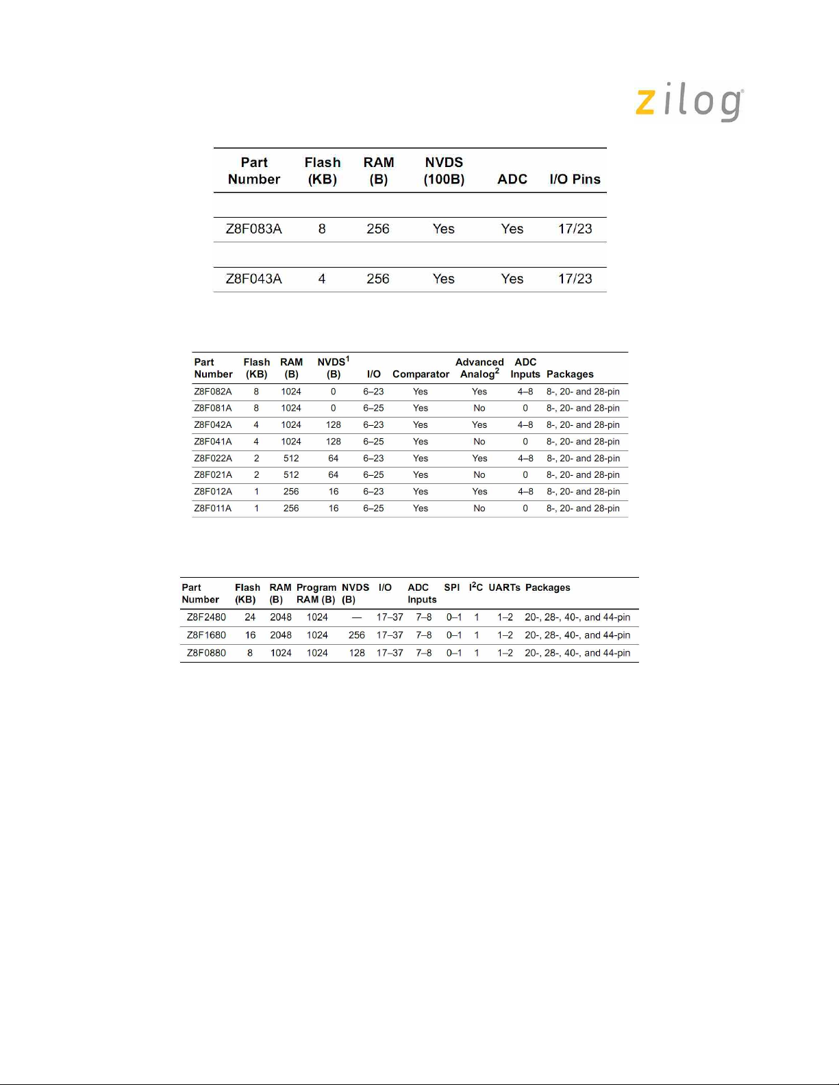
Part
Number
Z8F1232 12 256 No Yes
Z8F1233 12 256 No No
®
and Z8 Encore! XP®microcontroller acts like an Electrically
Flash
(KB)
RAM
(B)
NVDS
(64B)
ADC
Z8F0830 8 256 Yes Yes
Z8F0831 8 256 Yes No
Z8F0430 4 256 Yes Yes
Z8F0431 4 256 Yes No
Z8F0230 2 256 Yes Yes
Z8F0231 2 256 Yes No
Z8F0130 1 256 Yes Yes
Z8F0131 1 256 Yes No
Table 1. F0830 series Part Selection Guide
Page 2
NVDS Operation in the Z8 Encore!®and Z8 Encore! XP®MCU’s
Table 2. F083A series Part Se lection Guide
Application Note
Table3. F082A series Part Selection Guide
Table 4. F1680 series Part Selection Guide
The NVDS is implemented by special purpose Zilog® software stored in areas of program memory
not accessible to the user. These special-purpose routines use the flash memory to store and read
the data. The routines incorporate a dynamic addressing scheme to maximize the Write/Erase
endurance of the Flash.
The following routines are required to access the NVDS:
1. Write routine
2. Read routine
Both of these routines are accessed with a CALL instruction to a pre-defined address outside the
program memory that is not accessible to the user. Both the NVDS address and data are single-byte
values. These routines save the working register set before they are used (hence, 16 bytes of stack
space is needed). After finishing the call to these routines, the working register set of the user code
is recovered.
AN031001-0710 Page 2 of 9
Page 3

NVDS Operation in the Z8 Encore!®and Z8 Encore! XP®MCU’s
Application Note
This section discusses the following topics in detail:
• Interrupt Handling During NVDS Operation
• Flash Frequency Register Initialization
• NVDS Write Operation
• NVDS Read Operation
• Power Failure Protection
• Optimizing NVDS Memory Usage for Execution Speed
When the Z8 Encore! XP F042A Series device is in the DEBUG Mode, you can view the NVDS
memory locations by performing the following steps in ZDS II:
1. Navigate to View � Debug Windows � Memory. The Memory Window appears.
2. In the Memory Window, select the NVDS option from the Space drop down menu to view the
NVDS contents.
Interrupt Handling during NVDS Operation
Interrupts should be disabled before executing any NVDS operation (read or write) since they can
alter the working register and existing stack contents.
Flash Frequency Register Initialization
The Flash Frequency Registers must be programmed based on the system clock frequency.
void init_NVDS (void)
{
FFREQH = (SYSCLOCK/1000) >> 8;
FFREQL = (SYSCLOCK/1000) & 0xFF;
}
Note: SYSCLOCK is the system clock frequency in hertz. For proper NVDS operation, the flash frequency
registers should always have the proper value. Hence, whenever the system clock is changed, the flash
frequency register should also be upd ated. Improper values stored i n the flash frequency regis ter could result
to corrupted data in the NVDS area.
AN031001-0710 Page 3 of 9
Page 4

NVDS Operation in the Z8 Encore!®and Z8 Encore! XP®MCU’s
Application Note
NVDS Write Operation
Steps in writing a byte to the NVDS array:
1. Push the address of the NVDS array to be written on the stack
2. Push the data byte to be written on the stack
3. Issue a CALL instruction to the address of the Byte-Write routine
4. Pop the data byte and address off the stack
The write status byte resides in working register R0 after the CALL to the Byte Write instruction is
executed. The bit fields of this status byte are defined in Table 5 and Table 6. The write routine uses
13 bytes (F082A series) to 16 bytes (F0830, F083A and F1680 series) of stack space in addition to
the two bytes of address and data pushed by the user code.
Table 5. Write Status Byte (F0830, F083A a nd F1680 series)
Table 6. NVDS Status Byte (F082A series)
NVDS writes exhibit a non-uniform execution time (refer to the timing tables) due to the flash
memory architecture. A maintenance operation (every 200 writes for the F0830, F083A and F1680
series / every 400 to 500 writes for the F082A series) is necessary which takes up to 58 ms (F0830,
F083A and F1680 series) to 61 ms (F082A series) to complete. Slower system clock speeds result
in proportionally higher execution times. NVDS byte writes to invalid addresses (those exceeding the
NVDS array size) have no effect. Illegal write operations have a 2 µs (F082A series) to 7 µs
execution time (F0830, F083A and F1680 series).
V
= 2.7 to 3.6V
DD
T
= - 40ºC to +105ºC
A
Parameter Min Typ Max Units Notes
NVDS Byte Read Time 71
NVDS Byte Program Time 126
Data Retention 10
Endurance 100,000
Table 7. F0830 and F083A NVDS timing values
256 µs With system clock at 20 MH z
136 µs With system clock at 20 MH z
years 25ºC
Cycles Cumulative write cycles for entire
memory
AN031001-0710 Page 4 of 9
Page 5

NVDS Operation in the Z8 Encore!®and Z8 Encore! XP®MCU’s
V
= 2.7 to 3.6V
D
D
= 0ºC to +70ºC
T
A
T
= - 40ºC to +105ºC
A
Application Note
Parameter Min Typ Max Units Notes
NVDS Byte Read Time 34
NVDS Byte Program Time 0.171
Data Retention 20
Endurance 50,000
Table 8. F1680 NVDS timing val ues
519 µs With system clock at 20 MH z
39.7 ms With system clock at 20 MHz
years 25ºC
cycles Cumulative write cycles for entire
memory
NVDS Read Operation
Steps in reading a byte from the NVDS array:
1. Push the address of the NVDS array to be read
2. Issue a CALL instruction to the address of the Byte-Read routine
3. Pop the address off the stack
At the return from the sub-routine, the read byte resides in working register R0, and the read status
byte resides in working register R1. The bit fields of this status byte are defined in Table 6 and Table
9. The read routine uses 9 bytes (F082A series) to 16 bytes (F0830, F083A and F1680 series) of
stack space in addition to the 1 byte of address pushed by the user.
Table 9. Read Status Byte (F0830, F083A and F1680 series)
Because of the Flash memory architecture, NVDS reads exhibit a non-uniform execution time. A
read operation takes 71 µs - 258 µs (F0830, F083A and F1680 series) or 44 µs - 489 µs (F082A
series) for a system clock of 20 MHz. Slower system clock speeds result in proportionally higher
execution times. NVDS byte reads from invalid addresses (those exceeding the NVDS array size)
return 0xFF. Illegal read operations have an execution time of 2 µs (F082A series) to 6 µs (F0830,
F0383A and F1680 series). The status byte returned by the NVDS read routine is 0x00 for
successful read. If the status byte is non-zero, there is a corrupted value in the NVDS array at the
location being read. In this case, the value returned in R0 is the byte most recently written to the
array that does not have an error.
AN031001-0710 Page 5 of 9
Page 6

NVDS Operation in the Z8 Encore!®and Z8 Encore! XP®MCU’s
Application Note
VDD = 2.7 to 3.6V
T
= - 40ºC to +105ºC
A
Parameter Min Typ Max Units Notes
NVDS Byte Read Time 34
NVDS Byte Program Time 0.171
Data Retention 100
Endurance 160,000
Table 10. F082A NVDS timing values
519 µs With system clock at 20 MH z
39.7 ms With system clock at 20 MHz
years 25ºC
cycles Cumulative write cycles for entire
memory
AN031001-0710 Page 6 of 9
Page 7

NVDS Operation in the Z8 Encore!®and Z8 Encore! XP®MCU’s
Application Note
Power Failure Protection
The NVDS routines employ error checking mechanisms to ensure a power failure endangers only
the most recently written byte. Bytes previously written to the array are not modified. For this
protection to function, the VBO must be enabled and configured for a threshold voltage of 2.4 V or
greater.
A System Reset (such as a pin reset or watchdog timer reset) that occurs during a write operation
may alter the byte currently being written. All other bytes in the array are unaffected.
Optimizing NVDS Memory Usage for Execution Speed
As listed in Table 11 and Table 12, the NVDS read time varies drastically, this discrepancy being a
trade-off for minimizing the frequency of writes that require post-write page erases. The time
required for reading data from address N is a function of the number of writes to addresses; other
than N after the most recent write to N. Neglecting effects caused by page erases and results
caused by the initial condition in which the NVDS is blank, the rule of thumb is that every write since
the most recent page erase causes read times of unwritten addresses to increase by 0.8 µs, up to a
maximum of 258 µs.
Table 11. NVDS Latency (F0830, F083A and F1680 series)
Table 12. NVDS Latency (F082A series)
AN031001-0710 Page 7 of 9
Page 8

NVDS Operation in the Z8 Encore!®and Z8 Encore! XP®MCU’s
Application Note
If NVDS read performance is critical to your software architecture, you can
optimize your code for speed by using either of the methods listed below.
1. Periodically refresh all addresses that are used. This is the most useful method. The optimal
use of NVDS in terms of speed is to rotate the writes evenly among all addresses planned to
use, bringing all reads closer to the minimum read time. Because the minimum read time is
much less than the write time, however, actual speed benefits are not always realized.
2. Use as few unique addresses as possible. This helps to optimize the impact of refreshing.
Summary
This application note describes the basic NVDS routines and its principles. It also describes the
necessary procedures on how operate the NVDS and its features. It also shows the minimum and
maximum latency times for both read and write operations. The Z8 Encore! XP NVDS can be used
for data-logging applications, wherein data needs to be preserved even after power-off.
Flowchart
AN031001-0710 Page 8 of 9
Page 9

NVDS Operation in the Z8 Encore!®and Z8 Encore! XP®MCU’s
Application Note
Warning: DO NOT USE IN LIFE SUPPORT
LIFE SUPPORT POLICY
ZILOG'S PRODUCTS ARE NOT AUTHORIZED FOR USE AS CRITICAL COMPONENTS IN LIFE
SUPPORT DEVICES OR SYSTEMS WITHOUT THE EXPRESS PRIOR WRITTEN APPROVAL OF THE
PRESIDENT AND GENERAL COUNSEL OF ZILOG CORPORATION.
As used herein
Life support devices or systems are devices which (a) are intended for surgical implant into the body, or (b)
support or sustain life and whose failure to perfo rm when proper ly used in accordan ce with instru ction s for us e
provided in the labeling can be reasonably expected to result in a significant injury to the user. A critical
component is any component in a life support device or system whose failure to perform can be reasonably
expected to cause the failure of the life support dev i ce o r sy st em or to affect its safety or effectiveness.
Document Disclaimer
©2010 by Zilog, Inc. All rights reserved. Information in this publication concerning the devices, applications,
or technology described is intended to suggest possible uses and may be superseded. ZILOG, INC. DOES
NOT ASSUME LIABILITY FOR OR PROVIDE A REPRESENTATION OF ACCURACY OF THE
INFORMATION, DEVICES, OR TECHNOLOGY DESCRIBED IN THIS DOCUMENT. ZILOG ALSO
DOES NOT ASSUME LIABILITY FOR INTELLECTUAL PROPERTY INFRINGEMENT RELATED IN
ANY MANNER TO USE OF INFORM ATION, DE VICES, OR T ECHNOLOGY DES CRIBED HE REIN OR
OTHERWISE. The information contained within this document has been verified according to the general
principles of electrical and mechanical engineering.
Z8 Encore! XP is a registered trademark of Zilog, Inc. All other product or service names are the property of
their respective owners.
AN031001-0710 Page 9 of 9
 Loading...