

Page 1

Z89C00
16-BIT DIGITAL SIGNAL PROCESSOR
PRELIMINARY
DC 4083-00 1
ZILOG
FEATURES
P
RELIMINARY PRODUCT SPECIFICATION
■ 16-Bit Single Cycle Instructions
■ Zero Overhead Hardware Looping
■ 16-Bit Data
■ Ready Control for Slow Peripherals
■ Single Cycle Multiply/Accumulate (100 ns)
■ Six-Level Stack
■ 512 Words of On-Chip RAM
■ Static Single-Cycle Operation
■ 16-Bit I/O Port
■ 4K Words of On-Chip Masked ROM
■ Three Vectored Interrupts
■ 64K Words of External Program Address Space
■ Two Conditional Branch Inputs/Two User Outputs
■ 24-Bit ALU, Accumulator and Shifter
■ IBM
®
PC Development Tools
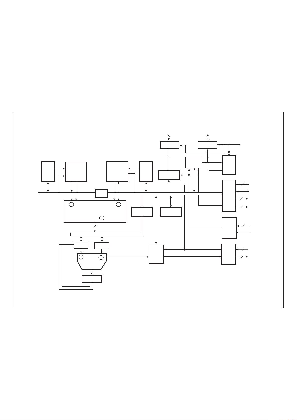
GENERAL DESCRIPTION
The Z89C00 is a second generation, 16-bit, fractional,
two’s complement CMOS Digital Signal Processor (DSP).
Most instructions, including multiply and accumulate,
are accomplished in a single clock cycle. The processor
contains 1 Kbyte of on-chip data RAM (two blocks of
256 16-bit words), 4K words of program ROM and 64K
words of program memory addressing capability. Also,
the processor features a 24-bit ALU, a 16 x 16 multiplier, a
24-bit Accumulator and a shifter. Additionally, the processor
contains a six-level stack, three vectored interrupts and
two inputs for conditional program jumps. Each RAM block
contains a set of three pointers which may be incremented
or decremented automatically to affect hardware looping
without software overhead. The data RAMs can be
simultaneously addressed and loaded to the multiplier for
a true single cycle multiply.
There is a 16-bit address and a 16-bit data bus for external
program memory and data, and a 16-bit I/O bus for
transferring data. Additionally, there are two general
purpose user inputs and two user outputs. Operation with
slow peripherals is accomplished with a ready input pin.
The clock may be stopped to conserve power.
Z89C00
16-BIT DIGITAL
SIGNAL PROCESSOR
Development tools for the IBM PC include a relocatable
assembler, a linker loader, and an ANSI-C compiler. Also,
the development tools include a simulator/debugger, a
cross assembler for the TMS320 family assembly code
and a hardware emulator.
To assist the user in understanding the Z89C00 DSP Q15
two's complement fractional multiplication, an application
note has been included in this product specification as an
appendix.
Notes:
All Signals with a preceding front slash, "/", are active Low, e.g.,
B//W (WORD is active Low); /B/W (BYTE is active Low, only).
Power connections follow conventional descriptions below:
Connection Circuit Device
Power V
CC
V
DD
Ground GND V
SS
Page 2
Z89C00
16-BIT DIGITAL SIGNAL PROCESSOR
PRELIMINARY
2 DC 4083-00
ZILOG
GENERAL DESCRIPTION (Continued)
Register
Pointer
0-2
16-Bit Bus
Stack
ACC
24-Bit Bus
ALU
B
A
256 Word
RAM
1
16 x16
Multiplier
24-bit
Instruction
Register
PD
256 Word
RAM
0
Register
Pointer
4-6
PC
16-bit
I/O
Port
PA
MUX
4K
Word
ROM
D-Bus
Status
(5)
Switch
Shifter
24
P-Bus
EXT15-EXT0
Ready
Interrupt
/ROMEN
16
3
UI1-UI0
UO1-UO0
2
2
User
Port
16
16
External Program ROM
16
16
PD15-PD0 PA15-PA0
INT2-INT0
/RESET
S-Bus
Switch
P
Y
X
ER//W, /EI
2
EA2-EA0
3
/RDYE
Figure 1. Functional Block Diagram
Page 3

Z89C00
16-BIT DIGITAL SIGNAL PROCESSOR
PRELIMINARY
DC 4083-00 3
ZILOG
789
654321
10
11
12
13
14
15
16
17
18
19
20
21
22
23
24
25
26
68 67 66 65 64 63 62 61
27 28 29 30 31 32 33 34 35 36 37 38 39 40 41 42 43
60
59
58
57
56
55
54
53
52
51
50
49
48
47
46
45
44
VSS
PD0
PD1
PD2
PD3
PD4
PD5
PD6
PD7
PD8
PD9
PD10
PD11
PD12
PD13
PD14
PD15
UO1
UO0
INT2
INT1
INT0
UI1
UI0
HALT
/ROMEN
CLK
/RES
/RDYE
ER//W
/EI
EA2
EA1
EA0
Z89C00
PA0
PA1
PA2
PA3
PA4
PA5
PA6
PA7
PA8
PA9
PA10
PA11
VDD
PA12
PA13
PA14
PA15
EXT 15
EXT14
EXT13
EXT12
EXT 11
EXT 10
EXT9
EXT8
EXT7
EXT6
EXT5
EXT4
VSS
EXT3
EXT1
EXT0
EXT2
Figure 2. 68-Pin PLCC Pin Assignments
Page 4

Z89C00
16-BIT DIGITAL SIGNAL PROCESSOR
PRELIMINARY
4 DC 4083-00
ZILOG
Table 1. 68-Pin PLCC Pin Identification
No. Symbol Function Direction
1-9 EXT15-EXT7 External data bus Input/Output
10 V
SS
Ground Input
11-26 PD15-PD0 Program data bus Input
27-38 PA11-PA0 Program address bus Output
39 V
DD
Power Supply Input
40-43 PA15-PA12 Program address bus Output
44-46 EA2-EA0 External address bus Output
47 /EI R/W for external bus Output
48 ER//W External bus direction Output
49 /RDYE Data ready Input
50 /RES Reset Input
51 CLK Clock Input
52 /ROMEN Enable ROM Input
53 HALT Stop execution Input
54-55 UI1-UI0 User inputs Input
56-58 INT2-INT1 Interrupts Input
59-60 UO1-UO0 User outputs Output
61-64 EXT3-EXT0 External data bus Input/Output
65 V
SS
Ground Input
66-68 EXT6-EXT4 External data bus Input/Output
PIN FUNCTIONS
CLK
Clock
(input). External clock. The clock may be
stopped to reduce power.
EXT15-EXT0
External Data Bus
(input/output). Data bus
for user defined outside registers such as an ADC or DAC.
The pins are normally in output mode except when the
outside registers are specified as source registers in the
instructions. All the control signals exist to allow a read or
a write through this bus.
ER//W
External Bus Direction
(output, active Low). Data
direction signal for EXT-Bus. Data is available from the
CPU on EXT15-EXT0 when this signal is Low. EXT-Bus is in
input mode (high-impedance) when this signal is High.
EA2-EA0
External Address
(output). User-defined register
address output. One of eight user-defined external registers
is selected by the processor with these address pins for
read or write operations. Since the addresses are part of
the processor memory map, the processor is simply
executing internal reads and writes.
/EI
Enable Input
(output). Write timing signal for EXT-Bus.
Data is read by the external peripheral on the rising edge
of /EI. Data is read by the processor on the rising edge of
CLK, not /EI.
HALT
Halt State
(input). Stop Execution Control. The CPU
continuously executes NOPs and the program counter
remains at the same value when this pin is held High. This
signal must be synchronized with CLK.
INT2-INT0
Three Interrupts
(rising edge triggered). Interrupt
request 2-0. Interrupts are generated on the rising edge of
the input signal. Interrupt vectors for the interrupt service
starting address are stored in the program memory locations
0FFFH for INT0, 0FFEH for INT1 and 0FFDH for INT2.
Priority is: 2 = lowest, 0 = highest.
PA15-PA0
Program memory address bus
(output). For up
to 64K x 16 external program memory. These lines are tristated during Reset Low.
Page 5

Z89C00
16-BIT DIGITAL SIGNAL PROCESSOR
PRELIMINARY
DC 4083-00 5
ZILOG
/RDYE
Data Ready
(input). User-supplied Data Ready
signal for data to and from external data bus. This pin
stretches the /EI and ER//W lines and maintains data on the
address bus and data bus. The ready signal is sampled
from the rising edge of the clock with appropriate setup
and hold times. The normal write cycle will continue from
the next rising clock only if ready is active.
UI1-UI0
Two Input Pins
(input). General purpose input
pins. These input pins are directly tested by the conditional
branch instructions. These are asynchronous input signals
that have no special clock synchronization requirements.
UO1-UO0
Two Output Pins
(output). General purpose
output pins. These pins reflect the inverted value of status
register bits S5 and S6. These bits may be used to output
data by writing to the status register.
PD15-PD0
Program Memory Data Input
(input). Instruc-
tions or data are read from the address specified by PD15PD0, through these pins and are executed or stored.
/RES
Reset
(input, active Low). Asynchronous reset signal.
A Low level on this pin generates an internal reset signal.
The /RES signal must be kept Low for at least one clock
cycle. The CPU pushes the contents of the PC onto the
stack and then fetches a new Program Counter (PC) value
from program memory address 0FFCH after the Reset
signal is released. RES Low tri-states the PA and PD bases.
/ROMEN
ROM Enable
(input). An active Low signal enables
the internal ROM. Program execution begins at 0000H
from the ROM. An active High input disables the ROM and
external fetches occur from address 0000H.
Program Memory. Programs of up to 4K words can be
masked into internal ROM. Four locations are dedicated to
the vector address for the three interrupts (0FFDH-0FFFH)
and the starting address following a Reset (0FFCH). Internal
ROM is mapped from 0000H to 0FFFH, and the highest
location for program is 0FFBH. If the /ROMEN pin is held
High, the internal ROM is inactive and the processor
executes external fetches from 0000H to FFFFH. In this
case, locations FFFC-FFFF are used for vector addresses.
Internal Data RAM. The Z89C00 has an internal 512 x
16-bit word data RAM organized as two banks of 256 x
16-bit words each, referred to as RAM0 and RAM1. Each
data RAM bank is addressed by three pointers, referred to
as Pn:0 (n = 0-2) for RAM0 and Pn:1 (n = 0-2) for RAM1. The
RAM addresses for RAM0 and RAM1 are arranged from
0-255 and 256-511, respectively. The address pointers,
which may be written to or read from, are 8-bit registers
connected to the lower byte of the internal 16-bit D-Bus
and are used to perform no overhead looping. Three
addressing modes are available to access the Data RAM:
register indirect, direct addressing, and short form direct.
These modes are discussed in detail later. The contents of
the RAM can be read or written in one machine cycle per
word without disturbing any internal registers or status
other than the RAM address pointer used for each RAM.
The contents of each RAM can be loaded simultaneously
into the X and Y inputs of the multiplier.
Registers. The Z89C00 has 12 internal registers and up to
an additional eight external registers. The external registers
are user definable for peripherals such as A/D or D/A or to
DMA or other addressing peripherals. External registers
are accessed in one machine cycle the same as internal
registers.
ADDRESS SPACE
Page 6

Z89C00
16-BIT DIGITAL SIGNAL PROCESSOR
PRELIMINARY
6 DC 4083-00
ZILOG
FUNCTIONAL DESCRIPTION
General. The Z89C00 is a high-performance Digital Signal
Processor with a modified Harvard-type architecture with
separate program and data memory. The design has been
optimized for processing power and minimizing silicon
space.
Instruction Timing. Many instructions are executed in one
machine cycle. Long immediate instructions and Jump or
Call instructions are executed in two machine cycles.
When the program memory is referenced in internal RAM
indirect mode, it takes three machine cycles. In addition,
one more machine cycle is required if the PC is selected as
the destination of a data transfer instruction. This only
happens in the case of a register indirect branch instruction.
An Acc + P => Acc; a(i) * b(j) → P calculation and
modification of the RAM pointers, is done in one machine
cycle. Both operands, a(i) and b(j), can be located in two
independent RAM (0 and 1) addresses.
Multiply/Accumulate. The multiplier can perform a 16-bit
x 16-bit multiply or multiply accumulate in one machine
cycle using the Accumulator and/or both the X and Y
inputs. The multiplier produces a 32-bit result, however,
only the 24 most significant bits are saved for the next
instruction or accumulation. The multiplier provides a flow
through operation whenever the X or Y register is updated,
an automatic multiply operation is performed and the P
register is updated. For operations on very small numbers
where the least significant bits are important, the data
should first be scaled by eight bits (or the multiplier and
multiplicand by four bits each) to avoid truncation errors.
Note that all inputs to the multiplier should be fractional
two’s complement 16-bit binary numbers. This puts them
in the range [–1 to 0.9999695], and the result is in 24-bits
so that the range is [–1 to 0.9999999]. In addition, if 8000H
is loaded into both X and Y registers, the resulting
multiplication is considered an illegal operation as an
overflow would result. Positive one cannot be represented
in fractional notation, and the multiplier will actually yield
the result 8000H x 8000H = 8000H (–1 x –1 = –1).
ALU. The 24-bit ALU has two input ports, one of which is
connected to the output of the 24-bit Accumulator. The
other input is connected to the 24-bit P-Bus, the upper
16 bits of which are connected to the 16-bit D-Bus. A shifter
between the P-Bus and the ALU input port can shift the
data by three bits right, one bit right, one bit left or no shift.
Hardware Stack. A six-level hardware stack is connected
to the D-Bus to hold subroutine return addresses or data.
The CALL instruction pushes PC+2 onto the stack. The
RET instruction pops the contents of the stack to the PC.
User Inputs. The Z89C00 has two inputs, UI0 and UI1,
which may be used by jump and call instructions. The jump
or call tests one of these pins and if appropriate, jumps to
a new location. Otherwise, the instruction behaves like a
NOP. These inputs are also connected to the status register
bits S10 and S11 which may be read by the appropriate
instruction (Figure 3).
User Outputs. The status register bits S5 and S6 connect
through an inverter to UO0 and UO1 pins and may be
written to by the appropriate instruction.
Interrupts. The Z89C00 has three positive edge triggered
interrupt inputs. An interrupt is acknowledged at the end of
any instruction execution. It takes two machine cycles to
enter an interrupt instruction sequence. The PC is pushed
onto the stack. A RET instruction transfers the contents
of the stack to the PC and decrements the stack pointer
by one word. The priority of the interrupts is 0 = highest,
2 = lowest.
Registers. The Z89C00 has 12 physical internal registers
and up to eight user-defined external registers. The EA2EA0 determines the address of the external registers. The
/EI, /RDYE, and ER//W signals are used to read or write
from the external registers.
Page 7

Z89C00
16-BIT DIGITAL SIGNAL PROCESSOR
PRELIMINARY
DC 4083-00 7
ZILOG
REGISTERS
There are 12 internal registers which are defined below:
Register Register Definition
P Output of Multiplier, 24-bit, Read Only
X X Multiplier Input, 16-bit
Y Y Multiplier Input, 16-bit
A Accumulator, 24-bit
SR Status Register, 16-bit
Pn:b Six Ram Address Pointers, 8-bit Each
PC Program Counter, 16-bit
The following are virtual registers as physical RAM does
not exist on the chip.
Register Register Definition
EXTn External registers, 16-bit
BUS D-Bus
Dn:b Eight Data Pointers
P holds the result of multiplications and is read only.
X and Y are two 16-bit input registers for the multiplier.
These registers can be utilized as temporary registers
when the multiplier is not being used. The contents of the
P register will change if X or Y is changed.
A is a 24-bit Accumulator. The output of the ALU is sent to
this register. When 16-bit data is transferred into this
register, it goes into the 16 MSB’s and the least significant
eight bits are set to zero. Only the upper 16 bits are
transferred to the destination register when the Accumulator
is selected as a source register in transfer instructions.
Pn:b are the pointer registers for accessing data RAM.
(n = 0,1,2 refer to the pointer number) (b = 0,1 refers to
RAM bank 0 or 1). They can be directly read from or written
to, and can point to locations in data RAM or indirectly to
Program Memory.
EXT(n) are external registers (n = 0 to 7). There are eight
16-bit registers here for accessing External data,
peripherals, or memory. Note that the actual register RAM
does not exist on the chip, but would exist as part of the
external device such as an ADC result latch.
BUS is a read-only register which, when accessed, returns
the contents of the D-Bus.
Dn:b refer to possible locations in RAM that can be used
as a pointer to locations in program memory. The
programmer decides which location to choose from two
bits in the status register and two bits in the operand. Thus,
only the lower 16 possible locations in RAM can be
specified. At any one time there are eight usable pointers,
four per bank, and the four pointers are in consecutive
locations in RAM. For example, if S3/S4 = 01 in the status
register, then D0:0/D1:0/D2:0/D3:0 refer to locations
4/5/6/7 in RAM bank 0. Note that when the data pointers are
being written to, a number is actually being loaded to Data
RAM, so they can be used as a limited method for writing
to RAM.
Page 8
Z89C00
16-BIT DIGITAL SIGNAL PROCESSOR
PRELIMINARY
8 DC 4083-00
ZILOG
REGISTERS (Continued)
Figure 3. Status Register
SR is the status register (Figure 3) which contains the ALU
status and certain control bits as shown in the following
table.
Status
Register Bit Function
S15 (N) ALU Negative
S14 (OV) ALU Overflow
S13 (Z) ALU Zero
S12 (L) Carry
S11 (UI1) User Input 1
S10 (UI0) User Input 0
S9 (SH3) MPY Output Shifted Right by Three Bits
S8 (OP) Overflow Protection
S7 (IE) Interrupt Enable
S6 (UO1) User Output 1
S5 (UO0) User Output 0
S4-3 “Short Form Direct” Bits
S2-0 (RPL) RAM Pointer Loop Size
RPL Description
S2 S1 S0 Loop Size
0 0 0 256
001 2
010 4
011 8
100 16
101 32
110 64
1 1 1 128
The status register may always be read in its entirety.
S15-S10 are set/reset by the hardware and can only be
read by software. S9-S0 can be written by software.
S7 S6 S5 S4 S3 S2 S1 S0S15 S14 S13 S12 S11 S10 S9 S8
N OV Z C UI1 UI0 SH3 OP IE UO1 UO0 RPL
"Short Form Direct" bits
User Output 0-1
Interrupt Enable
Overflow protection
MPY output shifted right
by 3 bit with sign extension
User Input 0-1
Carry
Zero
Overflow
Negative
0 0 0
0 0 1
0 1 0
0 1 1
1 0 0
1 0 1
1 1 0
1 1 1
256
2
4
8
16
32
64
128
Ram Pointer Loop Size
Read
and
Write
Read Only
Page 9
Z89C00
16-BIT DIGITAL SIGNAL PROCESSOR
PRELIMINARY
DC 4083-00 9
ZILOG
S15-S12 are set/reset by the ALU after an operation.
S11-S10 are set/reset by the user inputs. S6-S0 are control
bits described elsewhere. S7 enables interrupts. S8, if 0
(reset), allows the hardware to overflow. If S8 is set, the
hardware clamps at maximum positive or negative values
instead of overflowing. If S9 is set and a multiply instruction
is used, the shifter shifts the result three bits right with sign
extension.
PC is the Program Counter. When this register is assigned
as a destination register, one NOP machine cycle is added
automatically to adjust the pipeline timing.
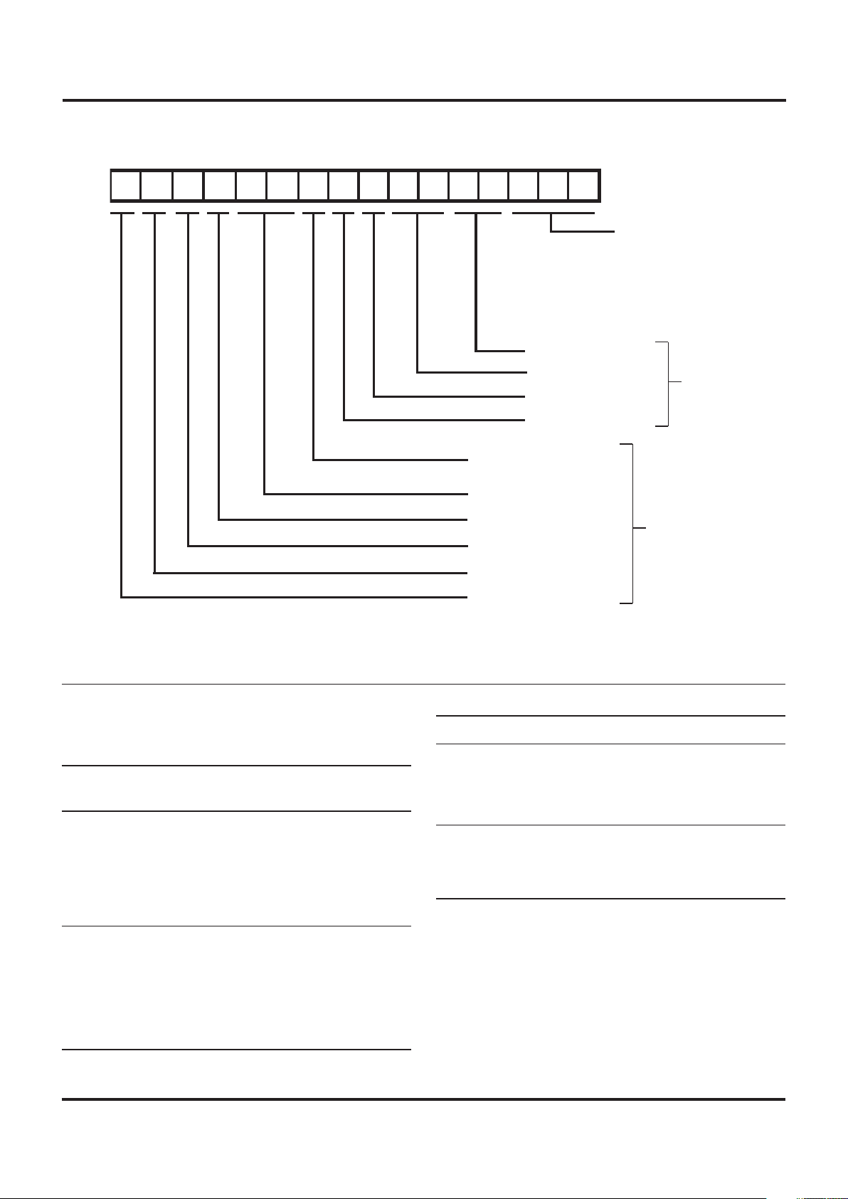
Figure 4. RAM, ROM, and Pointer Architecture
1. Register Indirect
Pn:b n = 0-2, b = 0-1
The most commonly used method is a register indirect
addressing method, where the RAM address is
specified by one of the three RAM address pointers (n)
for each bank (b). Each source/destination field in
Figures 5 and 8 may be used by an indirect instruction
to specify a register pointer and its modification after
execution of the instruction.
RAM Pointers
P0:0
P1:0
P2:0
%37
RAM0
256 x 16-Bit
@P1:0
%0321
%00
RAM1
256 x 16-Bit
%0321
%00
Internal ROM
4K x 16-Bit
%1234
%0000
%1000
%0321@@P1:0
@D0:1
RAM Pointers
P0:1
P1:1
P2:1
D0:0 %0321
D1:0
D2:0
D3:0
D0:1
D1:1
D2:1
D3:1
Data Pointers
%37 %04
S4 / S3 = 01
The following Instructions load
%1234 into the Accumulator:
LD A,@@P1:0
LD A,@D0:1
%FF %FF
D3 D2 D1 D0D8
bn1n0
RAM Pointer Register
Operation
RAM Bank
Figure 5. Indirect Register
RAM ADDRESSING
The address of the RAM is specified in one of three ways (Figure 4):
Page 10
Z89C00
16-BIT DIGITAL SIGNAL PROCESSOR
PRELIMINARY
10 DC 4083-00
ZILOG
The register pointer is specified by the first and second bits
in the source/destination field and the modification is
specified by the third and fourth bits according to the
following table:
D3-D0 Meaning
00xx NOP No Operation
01xx +1 Simple Increment
10xx –1/LOOP Decrement Modulo the Loop Count
11xx +1/LOOP Increment Modulo the Loop Count
xx00 P0:0 or P0:1 See Note a.
xx01 P1:0 or P1:1 See Note a.
xx10 P2:0 or P2:1 See Note a.
xx11 See Short Form Direct
Note:
a. If bit 8 is zero, P0:0 to P2:0 are selected; if bit 8 is one, P0:1 to P2:1
are selected.
When Loop mode is selected, the pointer to which the loop
is referring will cycle up or down, depending on whether a
–LOOP or +LOOP is specified. The size of the loop is
obtained from the least significant three bits of the Status
Register. The increment or decrement of the register is
accomplished modulo the loop size. As an example, if the
loop size is specified as 32 by entering the value 101 into
bits 2-0 of the Status Register (S2-S0) and an increment
+LOOP is specified in the address field of the instruction,
i.e., the RPi field is 11xx, then the register specified by RPi
will increment, but only the least significant five bits will be
affected. This means the actual value of the pointer will
cycle round in a length 32 loop, and the lowest or highest
value of the loop, depending on whether the loop is up or
down, is set by the three most significant bits. This allows
repeated access to a set of data in RAM without software
intervention. To clarify, if the pointer value is 10101001 and
if the LOOP = 32, the pointer increments up to 10111111,
then drops down to 10100000 and starts again. The upper
three bits remaining unchanged. Note that the original
value of the pointer is not retained.
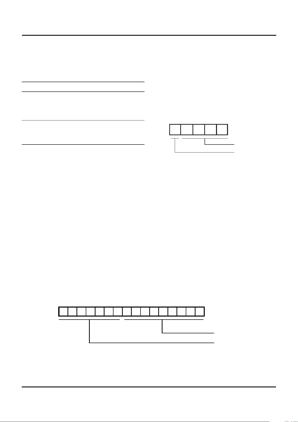
2. Direct Register
The second method is a direct addressing method.
The address of the RAM is directly specified by
the address field of the instruction. Because this
addressing method consumes nine bits (0-511) of the
instruction field, some instructions cannot use this
mode (Figure 6).
Figures 8 to 13 show the different register instruction
formats along with the two tables below Figure 8.
RAM ADDRESSING (Continued)
D7D6D5D4D3D2D1D0D8
D15
D14
D13
D12
D11
D10D9RAM Address
Opcode
S3 S2 D3 D2D8
bn1n0
RAM Address
RAM Bank
n2n3
Figure 7. Short Form Direct Address
3. Short Form Direct
Dn:b n = 0-3, b = 0-1
The last method is called Short Form Direct Addressing,
where one out of 32 addresses in internal RAM can be
specified. The 32 addresses are the 16 lower addresses
in RAM Bank 0 and the 16 lower addresses in RAM
Bank 1. Bit 8 of the instruction field determines RAM
Bank 0 or 1. The 16 addresses are determined by a
4-bit code comprised of bits S3 and S4 of the status
register and the third and fourth bits of the Source/
Destination field. Because this mode can specify a
direct address in a short form, all of the instructions
using the register indirect mode can use this mode
(Figure 7). This method can access only the lower 16
addresses in the both RAM banks and as such has
limited use. The main purpose is to specify a data
register, located in the RAM bank, which can then be
used to point to a program memory location. This
facilitates down-loading look-up tables, etc. from
program memory to RAM.
Figure 6. Direct Internal RAM Address Format
Page 11

Z89C00
16-BIT DIGITAL SIGNAL PROCESSOR
PRELIMINARY
DC 4083-00 11
ZILOG
INSTRUCTION FORMAT
B. Register Pointers Field
Source/Destination Meaning
00xx NOP
01xx +1
10xx –1/LOOP
11xx +1/LOOP
xx00 P0:0 or P0:1*
xx01 P1:0 or P1:1*
xx10 P2:0 or P2:1*
xx11 Short Form Direct
Mode
Figure 9. Short Immediate Data Load Format
RAM Bank selection
Destination field
Source field
D7D6D5D4D3D2D1D0D8
D15
D14
D13
D12
D11
D10D9Opcode
0 0 0
0 0 1
0 1 0
0 1 1
1 0 0
1 0 1
1 1 0
1 1 1
Reg. Pointer
P0:0
P1:0
P2:0
NA
P0:1
P1:1
P2:1
NA
D7D6D5D4D3D2D1D0D8
D15
D14
D13
D12
D11
D10
D9
Short Immediate Data
Opcode
0 0 0 1 1
Notes:
* If RAM Bank bit is 0, then Pn:0 are selected.
If RAM Bank bit is 1, then Pn:1 are selected.
** Read only.
Note:
Source/Destination fields can specify either register or
RAM addresses in RAM pointer indirect mode.
Figure 8. General Instruction Format
A. Registers
Source/Destination Register
0000 BUS**
0001 X
0010 Y
0011 A
0100 SR
0101 STACK
0110 PC
0111 P**
1000 EXT0
1001 EXT1
1010 EXT2
1011 EXT3
1100 EXT4
1101 EXT5
1110 EXT6
1111 EXT7
Page 12

Z89C00
16-BIT DIGITAL SIGNAL PROCESSOR
PRELIMINARY
12 DC 4083-00
ZILOG
INSTRUCTION FORMAT (Continued)
Figure 10. Immediate Data Load Format
Figure 11. Accumulator Modification Format
D7D6D5D4D3D2D1D0D8
D15
D14
D13
D12
D11
D10D91st Word
General Instruction Format
D7D6D5D4D3D2D1D0D8
D15
D14
D13
D12
D11
D10D92nd Word
Immediate Data
Condition Codes
0 0 0 0 TRUE
0 0 0 1 ---0 0 1 0 U01=0
0 0 1 1 UO1=0
0 1 0 0 C =0
0 1 0 1 Z=0
0 1 1 0 OV=0
0 1 1 1 N=0
1 x x x - - - 0 0 0 0 TRUE
0 0 0 1 - - - 0 0 1 0 UO0=1
0 0 1 1 UO1=1
0 1 0 0 C=1
0 1 0 1 Z=1
0 1 1 0 OV=1
0 1 1 1 N=1
1 x x x - - - -
D7D6D5D4D3D2D1D0D8
D15
D14
D13
D12
D11
D10
D9
0 0 0 0
0 0 0 1
0 0 1 0
0 0 1 1
0 1 0 0
0 1 0 1
0 1 1 0
0 1 1 1
ROR Rotate right
ROL Rotate left
SHR Shift right
SHL Shift left
INC Increment (LSB)
DEC Decrement (LSB)
NEG Negate
ABS Absolute
0 = Negative Condition
1 = Positive Condition
Opcode
1 0 0 1 0 0 0
ACC Modification Codes
Page 13

Z89C00
16-BIT DIGITAL SIGNAL PROCESSOR
PRELIMINARY
DC 4083-00 13
ZILOG
Figure 12. Branching Format
D7D6D5D4D3D2D1D0D8
D15
D14
D13
D12
D11
D10
D9
Condition Codes
0 0 0 0 TRUE
0 0 0 1 ---0 0 1 0 UO0=0
0 0 1 1 UO1=0
0 1 0 0 C=0
0 1 0 1 Z=0
0 1 1 0 OV=0
0 1 1 1 N=0
1 x x x - - - 0 0 0 0 TRUE
0 0 0 1 - - - 0 0 1 0 UO0=1
0 0 1 1 UO1=1
0 1 0 0 C=1
0 1 0 1 Z=1
0 1 1 0 OV=1
0 1 1 1 N=1
1 x x x - - - -
x x x x
Condition
0 = Negative
Condition
1 = Positive Conditio
n
Opcode
0 1 0 0 1 1 0
Branch
0 1 0 0 1 0 0 Call
1st Word
D7D6D5D4D3D2D1D0D8
D15
D14
D13
D12
D11
D10D92nd Word
Branch Address
x x 1 0
x x 1 1
x 1 x 0
x 1 x 1
1 x x 0
1 x x 1
Reset C flag
Set C flag
Reset IE Flag
(Interrupt enable)
Set IE Flag
Reset OP Flag
(Overflow protection)
Set OP Flag
D7D6D5D4D3D2D1D0D8
D15
D14
D13
D12
D11
D10D9x x x x
Opcode
1 0 0 1 0 1 0 Mod
Figure 13. Flag Modification Format
Page 14

Z89C00
16-BIT DIGITAL SIGNAL PROCESSOR
PRELIMINARY
14 DC 4083-00
ZILOG
ADDRESSING MODES
This section discusses the syntax of the addressing modes
supported by the DSP assembler. The symbolic name is
used in the discussion of instruction syntax in the instruction
descriptions.
Symbolic Name Syntax Description
<pregs> Pn:b Pointer Register
<dregs> Dn:b Data Register
(Points to RAM)
<hwregs> X,Y,PC,SR,P Hardware Registers
EXTn,A,BUS
<accind> @A Accumulator Memory Indirect
(Points to Program Memory)
<direct> <expression> Direct Address Expression
<limm> #<const exp> Long (16-bit) Immediate Value
<simm> #<const exp> Short (8-bit) Immediate Value
<regind> @Pn:b Pointer Register Indirect
(Points to RAM) @Pn:b+ Pointer Register Indirect with Increment
@Pn:b–LOOP Pointer Register Indirect with Loop Decrement
@Pn:b+LOOP Pointer register Indirect with Loop Increment
<memind> @@Pn:b Pointer Register Memory Indirect
(Points to Program Memory) @Dn:b Data Register Memory Indirect
@@Pn:b–LOOP Pointer Register Memory Indirect with Loop Decrement
@@Pn:b+LOOP Pointer Register Memory Indirect with Loop Increment
@@Pn:b+ Pointer Register Memory Indirect with Increment
There are eight distinct addressing modes for transfer of
data (Figure 4 and the table above).
<pregs>, <hwregs> These two modes are used for simple
loads to and from registers within the chip such as loading
to the Accumulator, or loading from a pointer register. The
names of the registers need only be specified in the
operand field. (Destination first then source)
<regind> This mode is used for indirect accesses to the
data RAM. The address of the RAM location is stored in the
pointer. The “@” symbol indicates “indirect” and precedes
the pointer, so @P1:1 tells the processor to read or write to
a location in RAM1, which is specified by the value in the
pointer.
<dregs> This mode is also used for accesses to the data
RAM but only the lower 16 addresses in either bank. The
4-bit address comes from the status register and the
operand field of the data pointer. Note that data registers
are typically used not for addressing RAM, but loading
data from program memory space.
Page 15

Z89C00
16-BIT DIGITAL SIGNAL PROCESSOR
PRELIMINARY
DC 4083-00 15
ZILOG
<memind> This mode is used for indirect, indirect accesses
to the program memory. The address of the memory is
located in a RAM location, which is specified by the value
in a pointer. So @@P1:1 tells the processor to read (write
is not possible) from a location in memory, which is
specified by a value in RAM, and the location of the RAM
is in turn specified by the value in the pointer. Note that the
data pointer can also be used for a memory access in this
manner, but only one “@” precedes the pointer. In both
cases the memory address stored in RAM is incremented
by one each time the addressing mode is used to allow
easy transfer of sequential data from program memory.
<accind> Similar to the previous mode, the address for the
program memory read is stored in the Accumulator. @A in
the second operand field loads the number in memory
specified by the address in A.
<direct> The direct mode allows read or write to data RAM
from the Accumulator by specifying the absolute address
of the RAM in the operand of the instruction. A number
between 0 and 255 indicates a location in RAM0, and a
number between 256 and 511 indicates a location in
RAM1.
<limm> This indicates a long immediate load. A 16-bit
word can be copied directly from the operand into the
specified register or memory.
<simm> This can only be used for immediate transfer of
8-bit data in the operand to the specified RAM pointer.
CONDITION CODES
The following table defines the condition codes supported
by the DSP assembler. If the instruction description
refers to the <cc> (condition code) symbol in one of its
addressing modes, the instruction will only execute if the
condition is true.
Name Description
NU1 Not User One
NZ Not zero
OV Overflow
PL Plus (Positive)
U0 User Zero
U1 User One
UGE Unsigned Greater Than or
Equal (Same as NC)
ULT Unsigned Less Than (Same as C)
Z Zero
Name Description
C Carry
EQ Equal (same as Z)
F False
IE Interrupts Enabled
MI Minus
NC No Carry
NE Not Equal (same as NZ)
NIE Not Interrupts Enabled
NOV Not Overflow
NU0 Not User Zero
Page 16

Z89C00
16-BIT DIGITAL SIGNAL PROCESSOR
PRELIMINARY
16 DC 4083-00
ZILOG
INSTRUCTION DESCRIPTIONS
Inst. Description Synopsis Operands Words Cycles Examples
ABS Absolute Value ABS[<cc>,]<src> <cc>,A 1 1 ABS NC,A
A 1 1 ABS A
ADD Addition ADD<dest>,<src> A,<pregs> 1 1 ADD A,P0:0
A,<dregs> 1 1 ADD A,D0:0
A,<limm> 2 2 ADD A,#%1234
A,<memind> 1 3 ADD A,@@P0:0
A,<direct> 1 1 ADD A,%F2
A,<regind> 1 1 ADD A,@P1:1
A,<hwregs> 1 1 ADD A,X
AND Bitwise AND AND<dest>,<src> A,<pregs> 1 1 AND A,P2:0
A,<dregs> 1 1 AND A,D0:1
A,<limm> 2 2 AND A,#%1234
A,<memind> 1 3 AND A,@@P1:0
A,<direct> 1 1 AND A,%2C
A,<regind> 1 1 AND A,@P1:2+LOOP
A,<hwregs> 1 1 AND A,EXT3
CALL Subroutine call CALL [<cc>,]<address> <cc>,<direct> 2 2 CALL Z,sub2
<direct> 2 2 CALL sub1
CCF Clear carry flag CCF None 1 1 CCF
CIEF Clear Carry Flag CIEF None 1 1 CIEF
COPF Clear OP flag COPF None 1 1 COPF
CP Comparison CP<src1>,<src2> A,<pregs> 1 1 CP A,P0:0
A,<dregs> 1 1 CP A,D3:1
A,<memind> 1 3 CP A,@@P0:1
A,<direct> 1 1 CP A,%FF
A,<regind> 1 1 CP A,@P2:1+
A,<hwregs> 1 1 CP A,STACK
A<limm> 2 2 CP A,#%FFCF
DEC Decrement DEC [<cc>,]<dest> <cc>A, 1 1 DEC NZ,A
A 1 1 DEC A
INC Increment INC [<cc>,] <dest> <cc>,A 1 1 INC PL,A
A 1 1 INC A
JP Jump JP [<cc>,]<address> <cc>,<direct> 2 2 JP NIE,Label
<direct> 2 2 JP Label
Page 17

Z89C00
16-BIT DIGITAL SIGNAL PROCESSOR
PRELIMINARY
DC 4083-00 17
ZILOG
Inst. Description Synopsis Operands Words Cycles Examples
LD Load destination LD<dest>,<src> A,<hwregs> 1 1 LD A,X
with source A,<dregs> 1 1 LD A,D0:0
A,<pregs> 1 1 LD A,P0:1
A,<regind> 1 1 LD A,@P1:1
A,<memind> 1 3 LD A,@D0:0
A,<direct> 1 1 LD A,124
<direct>,A 1 1 LD 124,A
<dregs>,<hwregs> 1 1 LD D0:0,EXT7
<pregs>,<simm> 1 1 LD P1:1,#%FA
<pregs>,<hwregs> 1 1 LD P1:1,EXT1
<regind>,<limm> 1 1 LD@P1:1,#1234
<regind>,<hwregs> 1 1 LD @P1:1+,X
<hwregs>,<pregs> 1 1 LD Y,P0:0
<hwregs>,<dregs> 1 1 LD SR,D0:0
<hwregs>,<limm> 2 2 LD PC,#%1234
<hwregs>,<accind> 1 3 LD X,@A
<hwregs>,<memind> 1 3 LD Y,@D0:0
<hwregs>,<regind> 1 1 LD A,@P0:0–LOOP
<hwregs>,<hwregs> 1 1 LD X,EXT6
Note: If X or Y register is the destination, an automatic multiply
operation is performed.
Note: The P register is Read Only and cannot be destination.
Note: LD EXTN, EXTN is not allowed.
Note: LD A, @A is not allowed.
MLD Multiply MLD<src1>,<src2>[,<bank switch>] <hwregs>,<regind> 1 1 MLD A,@P0:0+LOOP
<hwregs>,<regind>,<bank switch> 1 1 MLD A,@P1:0,OFF
<regind>,<regind> 1 1 MLD @P1:1,@P2:0
<regind>,<regind>,<bank switch> 1 1 MLD @P0:1,@P1:0,ON
Note: If src1 is <regind> it must be a bank 1 register.
Src2’s <regind must be a bank 0 register.
Note: <hwregs> for src1 cannot be X.
Note: For the operands <hwregs>, <regind> the <band switch> defaults to OFF.
For the operands <regind>, the <bank switch> defaults to ON.
MPYA Multiply and add MPYA <src1>,<src2>[,<bank switch>] <hwregs>,<regind> 1 1 MPYA A,@P0:0
<hwregs>,<regind>,<bank switch> 1 1 MPYA A,@P1:0,OFF
<regind>,<regind> 1 1 MPYA @P1:1,@P2:0
<regind>,<regind>,<bank switch> 1 1 MPYA@P0:1,@P1:0,ON
Note: If src1 is <regind> it must be a bank 1 register.
Src2’s <regind> must be a bank 0 register.
Note: <hwregs> for src1 cannot be X or A.
Note: For the operands <hwregs>, <regind> the <bank switch> defaults to
OFF. For the operands <regind>, the <bank switch> defaults to ON.
Page 18

Z89C00
16-BIT DIGITAL SIGNAL PROCESSOR
PRELIMINARY
18 DC 4083-00
ZILOG
INSTRUCTION DESCRIPTIONS (Continued)
Inst. Description Synopsis Operands Words Cycles Examples
MPYS Multiply and MPYS<src1>,<src2>[,<bank switch>] <hwregs>,<regind> 1 1 MPYS A,@P0:0
subtract <hwregs>,<regind>,<bank switch> 1 1 MPYS A,@P1:0,OFF
<regind>,<regind> 1 1 MPYS @P1:1,@P2:0
<regind>,<regind>,<bank switch> 1 1 MPYS @P0:1,@P1:0,ON
Note: If src1 is <regind> it must be a bank 1 register.
Src2’s <regind> must be a bank 0 register.
Note: <hwregs> for src1 cannot be X or A.
Note: For the operands <hwregs>, <regind> the <bank switch> defaults to OFF.
For the operands <regind>, <regind> the <bank switch> defaults to ON.
NEG Negate NEG <cc>,A <cc>, A 1 1 NEG MI,A
A 1 1 NEG A
NOP No operation NOP None 1 1 NOP
OR Bitwise OR OR <dest>,<src> A, <pregs> 1 1 OR A,P0:1
A, <dregs> 1 1 OR A, D0:1
A, <limm> 2 2 OR A,#%2C21
A, <memind> 1 3 OR A,@@P2:1+
A, <direct> 1 1 OR A, %2C
A, <regind> 1 1 OR A,@P1:0–LOOP
A, <hwregs> 1 1 OR A,EXT6
POP Pop value POP <dest> <pregs> 1 1 POP P0:0
from stack <dregs> 1 1 POP D0:1
<regind> 1 1 POP @P0:0
<hwregs> 1 1 POP A
PUSH Push value PUSH <src> <pregs> 1 1 PUSH P0:0
onto stack <dregs> 1 1 PUSH D0:1
<regind> 1 1 PUSH @P0:0
<hwregs> 1 1 PUSH BUS
<limm> 2 2 PUSH #12345
<accind> 1 3 PUSH @A
<memind> 1 3 PUSH @@P0:0
RET Return from subroutine RET None 1 2 RET
RL Rotate Left RL <cc>,A <cc>,A 1 1 RL NZ,A
A 1 1 RL A
RR Rotate Right RR <cc>,A <cc>,A 1 1 RR C,A
A 1 1 RR A
Page 19

Z89C00
16-BIT DIGITAL SIGNAL PROCESSOR
PRELIMINARY
DC 4083-00 19
ZILOG
Inst. Description Synopsis Operands Words Cycles Examples
SCF Set C flag SCF None 1 1 SCF
SIEF Set IE flag SIEF None 1 1 SIEF
SLL Shift left SLL [<cc>,]A 1 1 SLL NZ,A
logical A 1 1 SLL A
SOPF Set OP flag SOPF None 1 1 SOPF
SRA Shift right SRA<cc>,A <cc>,A 1 1 SRA NZ,A
arithmetic A 1 1 SRA A
SUB Subtract SUB<dest>,<src> A,<pregs> 1 1 SUB A,P1:1
A,<dregs> 1 1 SUB A,D0:1
A,<limm> 2 2 SUB A,#%2C2C
A, <memind> 1 3 SUB A,@D0:1
A, <direct> 1 1 SUB A,%15
A, <regind> 1 1 SUB A,@P2:0-LOOP
A, <hwregs> 1 1 SUB A,STACK
XOR Bitwise exclusive OR XOR <dest>,<src> A, <pregs> 1 1 XOR A,P2:0
A, <dregs> 1 1 XOR A,D0:1
A, <limm> 2 2 XOR A,#13933
A, <memind> 1 3 XOR A,@@P2:1+
A, <direct> 1 1 XOR A,%2F
A, <regind> 1 1 XOR A,@P2:0
A, <hwregs> 1 1 XOR A,BUS
Bank Switch Enumerations. The third (optional) operand
of the MLD, MPYA and MPYS instructions represents
whether a bank switch is set on or off. To more clearly
represent this, two keywords are used (ON and OFF)
which state the direction of the switch. These keywords are
referred to in the instruction descriptions through the
<bank switch> symbol.
Page 20

Z89C00
16-BIT DIGITAL SIGNAL PROCESSOR
PRELIMINARY
20 DC 4083-00
ZILOG
ABSOLUTE MAXIMUM RATINGS
Symbol Description Min Max Units
V
CC
Supply Voltage(*) –0.5 7.0 V
T
STG
Storage Temp. –65° +150° C
T
A
Oper. Ambient Temp. † C
Notes:
* Voltages on all pins with respect to ground.
† See Ordering Information
Stresses greater than those listed under Absolute Maximum
Ratings may cause permanent damage to the device. This
is a stress rating only; operation of the device at any
condition above those indicated in the operational sections
of these specifications is not implied. Exposure to absolute
maximum rating conditions for extended period may affect
device reliability.
STANDARD TEST CONDITIONS
The characteristics listed below apply for standard test
conditions as noted. All voltages are referenced to ground.
Positive current flows into the referenced pin (Test Load
Diagram, Figure 14).
+5V
From Output
Under Test
150 pF 9.1 K Ω
2.1 K Ω
Figure 14. Test Load Diagram
DC ELECTRICAL CHARACTERISTICS
(V
CC
= 5V ± 5%, TA = 0°C to +70°C unless otherwise specified)
Symbol Parameter Condition Min. Max. Units
I
CC
Supply Current V
CC
= 5.25V 60 mA
fclock = 10 MHz
I
CC1
Halt Mode V
CC
= 5.25V 1 5 mA
fclock = 0 MHz (stopped)
V
IH
Input High Level 0.9 V
CC
V
V
IL
Input Low Level 0.1 V
CC
V
I
IL
Input Leakage 1 µA
V
OH
Output High Voltage I
OH
= –100 µAV
CC
– 0.2 V
V
OL
Output Low Voltage I
OL
= 0.5 mA 0.5 V
I
FL
Output Floating Leakage Current 5 µA
Page 21

Z89C00
16-BIT DIGITAL SIGNAL PROCESSOR
PRELIMINARY
DC 4083-00 21
ZILOG
AC ELECTRICAL CHARACTERISTICS
(VCC = 5V ± 5%, TA = 0°C to +70°C unless otherwise specified)
No. Symbol Parameter Min. Max. Units
1 TCY Clock Cycle Time 100 1000 ns
2 PWW Clock Pulse Width 45 ns
3 Tr Clock Rise Time 2 4 ns
4 Tf Clock Fall Time 2 4 ns
5 TEAD EA,ER//W Delay from CK 9 33 ns
6 TXVD EXT Data Output Valid from CLK 5 27 ns
7 TXWH EXT Data Output Hold from CLK 6 22 ns
8 TXRS EXT Data Input Setup Time 15 ns
9 TXRH EXT Data Input Hold from CLK 5 15 ns
10 TIEDR /EI Delay Time from Rising CLK Edge 3 15 ns
11 TIEDF /EI Delay Time from Falling CLK Edge 0 23 ns
12 TINS Interrupt Setup Time 5 ns
13 TINL Interrupt Hold Time 15 ns
14 TPAD PA Delay from CLK 5 22 ns
15 TPDS PD Input Setup Time 20 ns
16 TPDH PD Input Hold Time 20 28 ns
17 TCTLS Halt Setup Time 5 ns
18 TCTLH Halt Hold Time 20 ns
19 RDYS Ready Setup Time 10 ns
20 RDYH Ready Hold Time 7 ns
Page 22

Z89C00
16-BIT DIGITAL SIGNAL PROCESSOR
PRELIMINARY
22 DC 4083-00
ZILOG
AC TIMING DIAGRAM
CLK
/EI
ER//W
EXT15-EXT0
EA2-EA0
V alid Address Out
V alid
Data Out
/RDYE
EXT Bus:
Output
1 7
2
6
5
11 10
5
5
Figure 15. Write To External Device Timing
Page 23

Z89C00
16-BIT DIGITAL SIGNAL PROCESSOR
PRELIMINARY
DC 4083-00 23
ZILOG
CLK
/EI
ER//W
EXT15-EXT0
EA2-EA0
V alid Address Out
V alid
Data In
/RDYE
EXT Bus:
Input
1 9
8
16
5
10
5
1
2
Figure 16. Read From External Device Timing
Page 24

Z89C00
16-BIT DIGITAL SIGNAL PROCESSOR
PRELIMINARY
24 DC 4083-00
ZILOG
AC TIMING DIAGRAM
CLK
/EI
ER//W
EXT15-EXT0
EA2-EA0
V alid Address Out
Valid Data Out
/RDYE
EXT Bus: Output
20
19
10
5
7
6
1
2
11
5
Figure 17. Write To External Device Timing
(/RDYE used to hold data one clock cycle)*
Note: * /RDYE is checked during rising edge of clock.
Page 25

Z89C00
16-BIT DIGITAL SIGNAL PROCESSOR
PRELIMINARY
DC 4083-00 25
ZILOG
CLK
/EI
ER//W
EXT15-EXT0
EA2-EA0
V alid Address Out
Valid Data In
/RDYE
EXT Bus: Input
20
19
5
10
9
82
11
5
1
Figure 18. Read From External Device Timing
(/RDYE used to hold data one clock cycle)*
Note: * /RDYE is checked during rising edge of clock.
Page 26

Z89C00
16-BIT DIGITAL SIGNAL PROCESSOR
PRELIMINARY
26 DC 4083-00
ZILOG
AC TIMING DIAGRAM
PD15-PD0
CLK
PA15-PA0
HALT
1
2
15
14
16
14
1817
Figure 19. Memory Port Timing
INT2-INT0
HALT
CLK
1
2
12
13
18
17
Figure 20. Interrupt and HALT Timing
Page 27
Z89C00
16-BIT DIGITAL SIGNAL PROCESSOR
PRELIMINARY
DC 4083-00 27
ZILOG
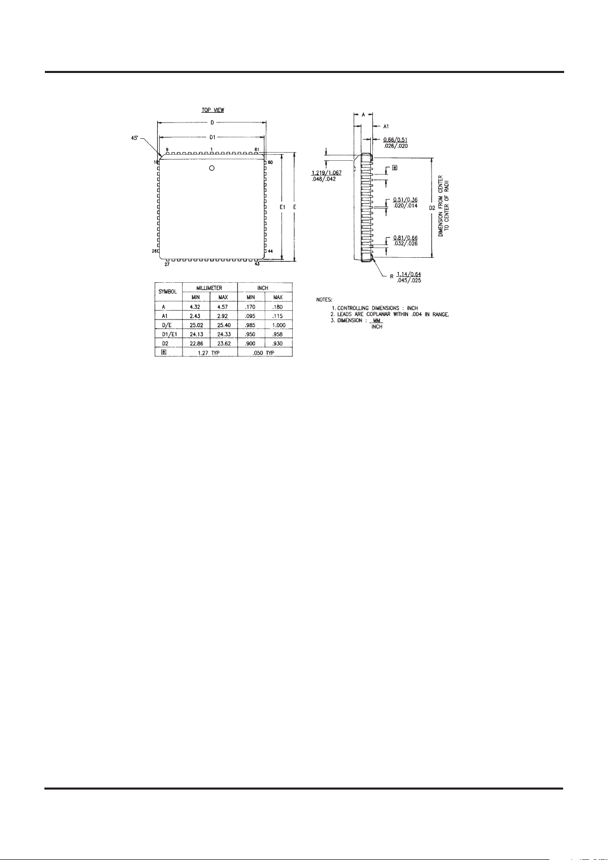
PACKAGE INFORMATION
68-Pin PLCC Package Diagram
Page 28

Z89C00
16-BIT DIGITAL SIGNAL PROCESSOR
PRELIMINARY
28 DC 4083-00
ZILOG
ORDERING INFORMATION
Z89C00
10 MHz
68-pin PLCC
Z89C0010VSC
15 MHz
68-pin PLCC
Z89C0015VSC
For fast results, contact your local Zilog sales office for assistance in ordering the part desired.
Package
V = Plastic Leaded Chip Carrier
Temperature
S = 0°C to +70°C
Speeds
10 = 10 MHz
15 = 15 MHz
Environmental
C = Plastic Standard
Example:
Z 89C00 10 V S C
Environmental Flow
Temperature
Package
Speed
Product Number
Zilog Prefix
is a Z89C00, 10 MHz, PLCC, 0°C to +70°C, Plastic Standard Flow
Zilog’s products are not authorized for use as critical components in life support devices or systems unless a specific written
agreement pertaining to such intended use is executed between
the customer and Zilog prior to use. Life support devices or
systems are those which are intended for surgical implantation
into the body, or which sustains life whose failure to perform,
when properly used in accordance with instructions for use
provided in the labeling, can be reasonably expected to result in
significant injury to the user.
Zilog, Inc. 210 East Hacienda Ave.
Campbell, CA 95008-6600
Telephone (408) 370-8000
Telex 910-338-7621
FAX 408 370-8056
Internet: http://www.zilog.com
© 1997 by Zilog, Inc. All rights reserved. No part of this document
may be copied or reproduced in any form or by any means
without the prior written consent of Zilog, Inc. The information in
this document is subject to change without notice. Devices sold
by Zilog, Inc. are covered by warranty and patent indemnification
provisions appearing in Zilog, Inc. Terms and Conditions of Sale
only. Zilog, Inc. makes no warranty, express, statutory, implied or
by description, regarding the information set forth herein or
regarding the freedom of the described devices from intellectual
property infringement. Zilog, Inc. makes no warranty of merchantability or fitness for any purpose. Zilog, Inc. shall not be
responsible for any errors that may appear in this document.
Zilog, Inc. makes no commitment to update or keep current the
information contained in this document.
 Loading...