

FEATURES
PRELIMINARY
P
RELIMINARY
C
USTOMER PROCUREMENT SPECIFICATION
Z89462
16-BIT, FIXED-POINT
DIGITAL SIGNAL PROCESSOR
Z89462
CP95DSP0400
Prog. RAM Prog./Data Data RAM Speed
Part (K Words) (K Words) (Words) (MHz)
Z89462 1 64 512 20, 40
■ 100-Pin QFP and 124-Pin PGA Packages
■ 0°C to +70°C Temperature Range
■ 3.3- to 5.0-Volt Operating Range
40 MHz Operation @ 5.0V
20 MHz Operation @ 3.3V
■ Six RAM Pointers for 4K-Word RAM Banks
■ Three Maskable Vectored Interrupts, Edge or Level
Trigger Selectable
GENERAL DESCRIPTION
The Z89462 is a high-performance Digital Signal Processor
(DSP) optimized for processing and transferring data. This
enhanced processor provides an upward migration path
for its Z89C00/Z89321 predecessors.
The DSP provides three 12-bit Register Pointers for each
RAM bank. These pointers may be incremented or
decremented automatically to implement circular buffers
without software overhead.
Three prioritized and individually maskable interrupts are
provided for use by external peripherals requiring service
from the DSP. The interrupt inputs can be individually
conditioned for edge or level trigger. Acknowledgement of
an activated interrupt occurs at the end of an instruction
execution.
■ Enhanced Instruction Set
■ Single-Cycle Instruction Execution
■ Four-Stage Pipeline
On-Board Peripherals
■ Dual 8/16-Bit CODEC Interface
■ Wait-State Generator
■ Two 16-Bit Timer/Counters
■ Dynamic Program Bus Sizing
Two banks of 512 x 16-bit data RAM are available.
Expansion of the on-chip data RAM is provided through
future upgrades.
External interfaces include Address Bus and Data Bus for
external Program Memory, Address Bus and Data Bus for
external Data Memory, three vectored interrupt ports, and
two input/two output user ports.
Notes:
All Signals with a preceding front slash, "/", are active Low, e.g.,
B//W (WORD is active Low); /B/W (BYTE is active Low, only).
Power connections follow conventional descriptions below:
Connection Circuit Device
Power V
Ground GND V
CC
V
DD
SS
CP95DSP0400 (8/95)
1
PRELIMINARY
GENERAL DESCRIPTION (Continued)
Z89462
CP95DSP0400
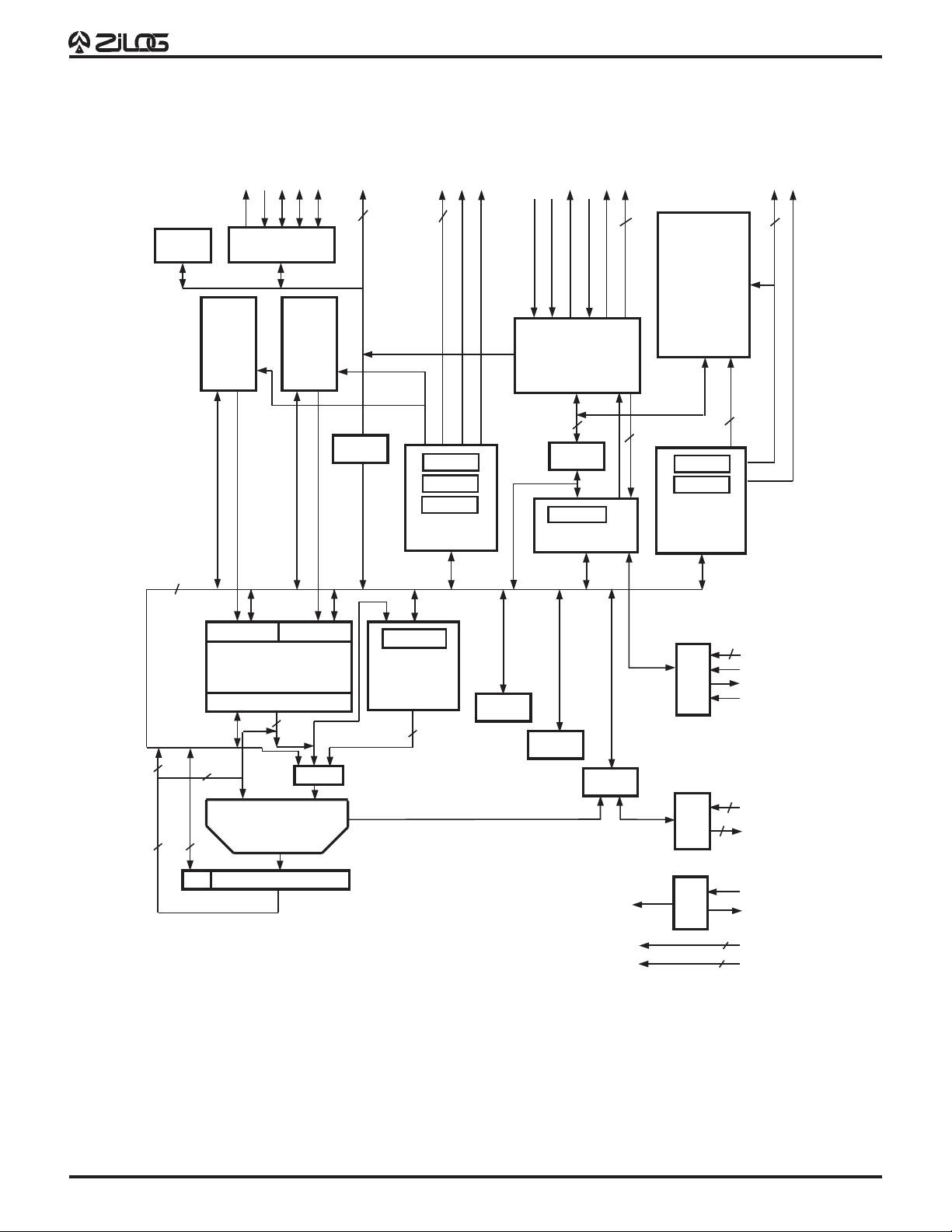
IDB
Timers
RAM0
512W
TxD
SCLK
RxD
CODEC
FS0
RAM1
512W
FS1
MD15-MD0
16
MDR
MA15-MA0
MRD//WR
16
MAR
SP
FPR
MBUS_RAM01
Control
/MDS
AIT
AIT
/PDS
/PW
/MW
WSG_BYWD
16
PDR
IR
DSP Control
/PALSB
/PDSZE
ds
PD15-PD0
16
2
waits
Program
RAM
1KW
rd,wr
PAR
PC
PBUS
Control
A0
PRD//WR
PA15-P
16
2
16
32
16
X
Multiplier
PH
32
BA
8
AE
AH AL
Y
PPL
32
PB BFB
MUX
ALU
A
BFR
Bit
Field
Unit
32
Repeat
Count
Reg
RC
CR
Control
Reg
SR
Status
Reg
INT
CTL
User
Port
CLK
GEN
2
8
2
8
3
INT2-0
/HLTHW
/HLTOUT
/RESET
UI1-0
UO1-0
CLKIN
CLK
VDD
VSS
Functional Block Diagram
2
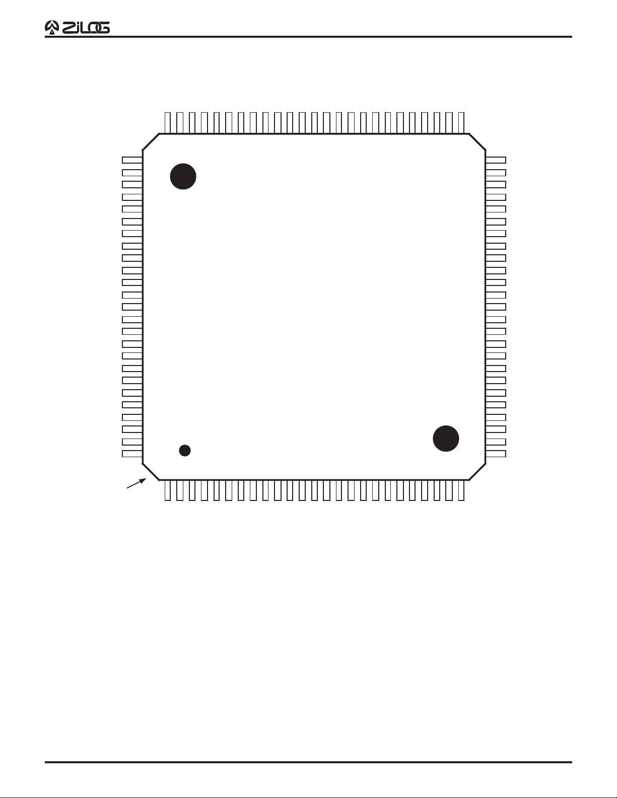
PIN DESCRIPTION
PD15
PD14
PD13
/HLTHW
PRELIMINARY
PD12
PD11
PD10
/HLTOUT
PD9
PD8
/RESET
PD7
CKIN
PD6
VSSI
PD5
CLK
/PWAIT
PD4
INT0
PD3
PDSZE
INT1
VSSP
Z89462
CP95DSP0400
VDDP
MA0
PA0
MA1
PA1
MA2
PA2
MA3
PA3
VDDP
VSSP
MA4
MA5
MA6
MA7
VSSI
MRD//WR
/MDS
/MWAIT
MA8
PA4
MA9
VDDP
VSSP
PA5
MA10
75 51
76
80
85
6070 5565
Z89462
90
95
100
100-Pin VQFP
50
26
45
40
35
30
PD2
PALSB
INT2
PD5
PRD//WR
UI1
PD1
UI0
PD0
UO1
UO0
MD15
VDDI
MD14
MD13
VSSP
VDDP
MD12
MD11
MD10
MD9
PA15
MD8
PA14
MD7
Pin 1
125
PA6
MA11
5
PA7
PA8
MA13
MA12
10 15 20
PA9
MA14
VDDP
VSSP
MA15
MD0
VDDI
MD1
MD2
MD3
PA10
MD4
VSSP
PA12
MD6
PA13
MD5
PA11
VDDP
100-Pin VQFP Pin Assignments
3
 Loading...