


ZILOG
GENERAL DESCRIPTION
PRELIMINARY
P
RELIMINARY
C
USTOMER PROCUREMENT SPECIFICATION
Z89390
16-BIT DIGITAL
SIGNAL PROCESSOR
CPS DC-9030-01
Z89390
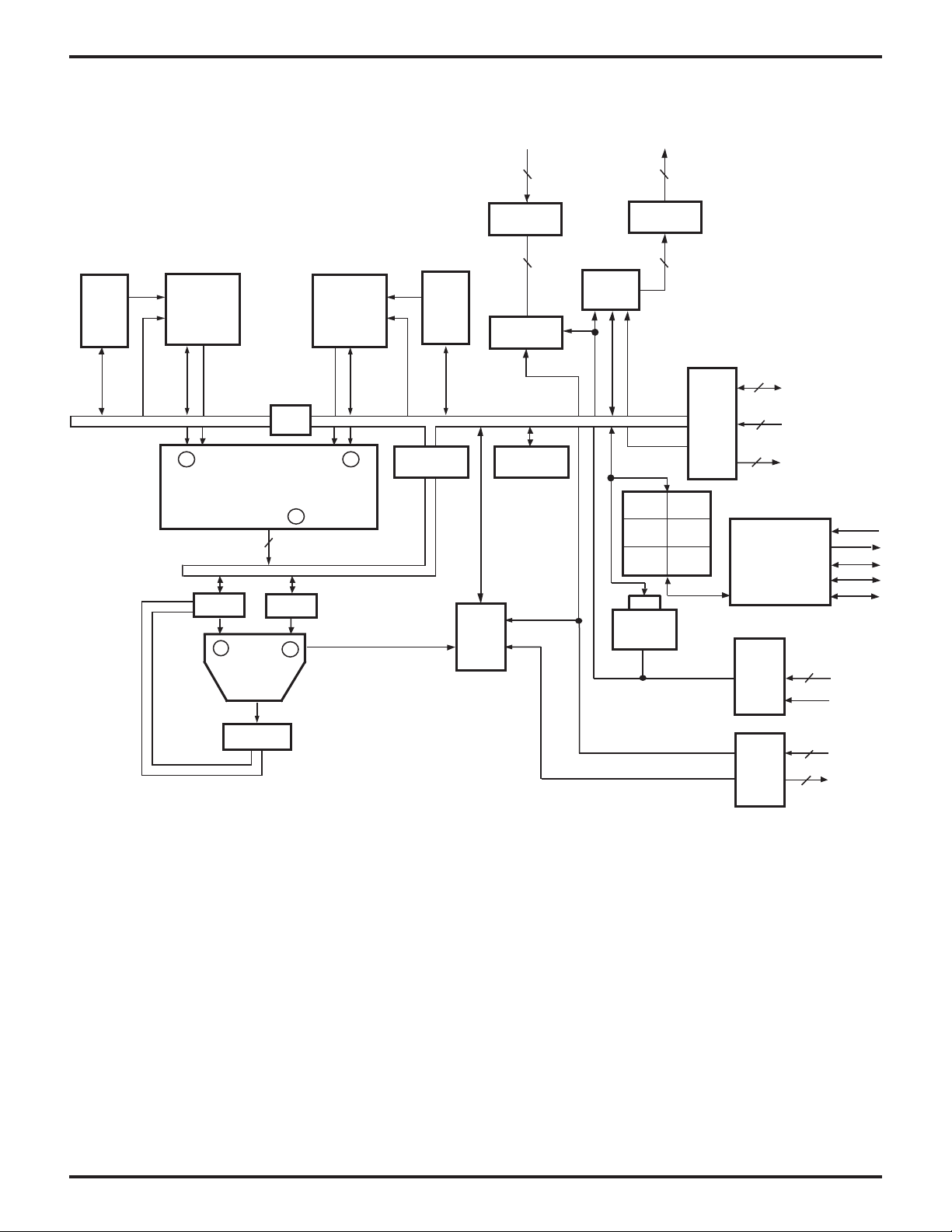
The Z89390 is a CMOS Digital Signal Processor (DSP).
Single-cycle instruction execution and a Harvard bus
structure promotes efficient algorithm execution. The
processor contains 512 word data RAM and 64K word of
external program address space is accessible. Six register
pointers provide circular buffering capabilities and dual
operand fetching. Three vectored interrupts are
complemented by a six level stack. The CODEC interface
enables high-speed transfer rates to accommodate digital
audio and voice data. A dedicated Counter/Timer provides
the necessary timing signals for the CODEC interface. An
additional 13-bit timer is available for general-purpose
use.
The Z89390 is optimized to accommodate intricate signal
processing algorithms. The 20-MIP operating performance
and efficient architecture provides real-time execution.
Compression, filtering, frequency detection, audio, voice
detection/synthesis and other available algorithms can all
be accommodated. The on-board peripherals provide
additional cost advantages.
Development tools for the IBM PC include a relocatable
assembler, a linker loader debugger.
Notes:
All Signals with a preceding front slash, "/", are active Low, e.g.,
B//W (WORD is active Low); /B/W (BYTE is active Low, only).
Power connections follow conventional descriptions below:
Connection Circuit Device
Power V
Ground GND V
CC
V
DD
SS
DC 9030-00 1
ZILOG
PRELIMINARY
GENERAL DESCRIPTION (Continued)
External Program ROM
PD15-PD0
16 16
CPS DC-9030-01
Z89390
PA15-PA0
Register
Pointer
0-2
S-Bus
256 Word
RAM
0
X
16-Bit Bus
16 x16
Multiplier
24-bit
24-Bit Bus
MUX
B A
ALU
Switch
P
24
Shifter
256 Word
P Bus
RAM
1
Y
Register
Pointer
Switch
4-6
Status
(5)
PD
16 16
Instruction
Register
D Bus
Stack
PC
Ready
EXT5-1 EXT5-2
EXT6-1
EXT7-1
EXT4
13-Bit
Timer
PA
EXT6-2
EXT7-2
16-bit
I/O
Port
16
CODEC
Interface
Interrupt
EXT0-15
WAIT, RD/WR, /OS
3
EA0-2
3
RXD
TXD
SCLK
FS0
FS1
/INTO-2
/RESET
ACC
Note: EXT5, EXT6, and INTERRUPT1 are used for the CODEC Interface. EXT4 and
INTERRUPT2 are used for the 13-bit timer.
Z89391 Functional Block Diagram
User
Port
2
UI0-1
2
UO0-1
2 DC 9030-00
ZILOG
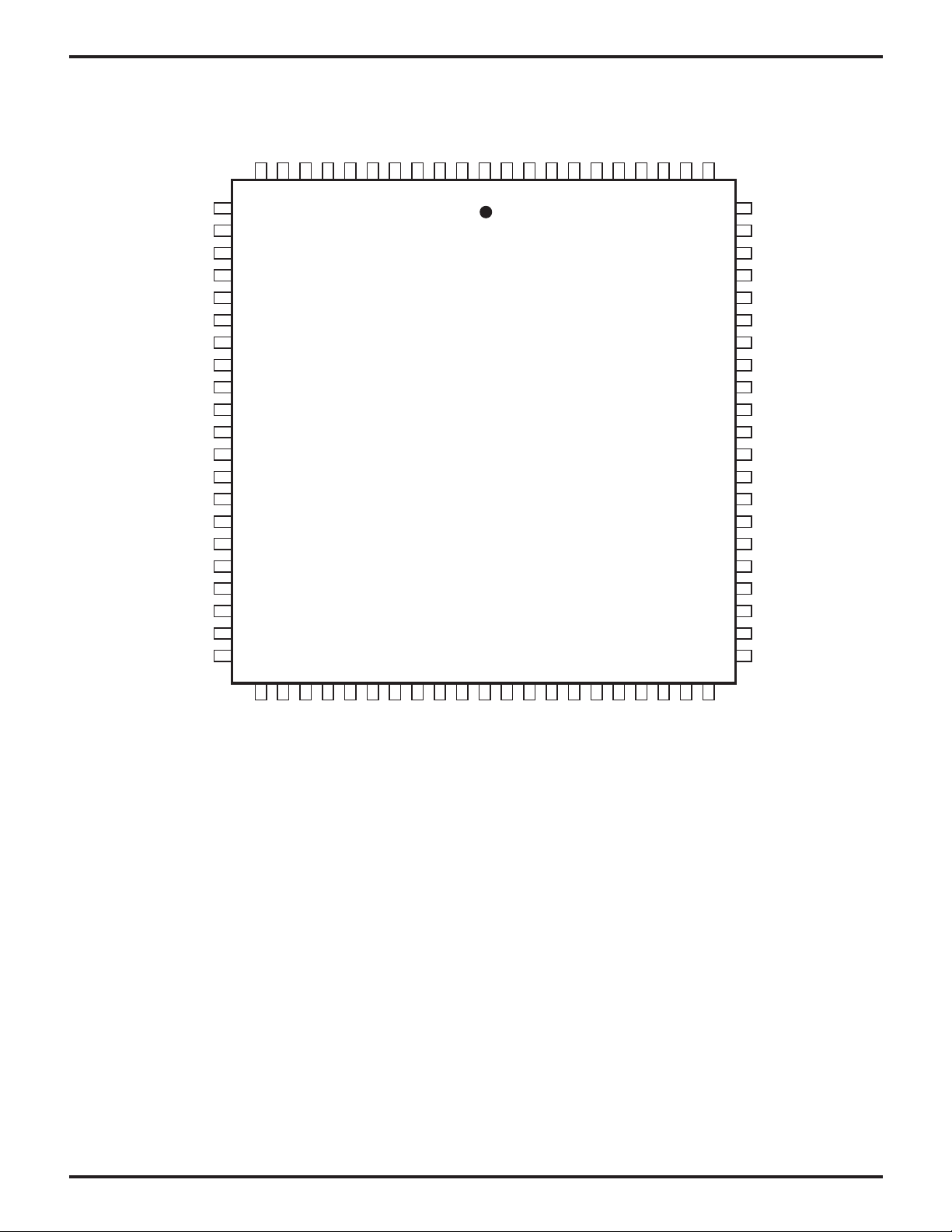
PIN DESCRIPTION
PRELIMINARY
CPS DC-9030-01
Z89390
VSS
EXT3
PA8
EXT4
PA9
VSSP
EXT5
PA10
EXT6
PA11
EXT7
TXD
PA12
EXT8
PA13
EXT9
VSS
PA14
EXT10
PA15
VCC
32
12
33
11
N/C
EXT15
PA7
VSS
PA6
EXT14
PA5
EXT12
EXT13
PA4
Z89390
84-Pin PLCC
42 43
RXD
VSS
184
PA0
VSS
VCC
PA1
PA3
EXT2
PA2
EXT1
EXT0
75
VSS
74
PD15
FS1
PD14
UO1
PD13
UO0
PD12
INT0
FS0
HALT
PD11
CLK
/D5
PD10
VDDP
PD9
EA2
PD8
EA1
54
VDD
53
VSS
PD0
UI0
PD1
EXT11
INT2
INT1
SCLK
VDD
RD//WR
UI1
PD3
PD2
PD4
WAIT
PD5
PD6
/RESET
EA0
PD7
VCC
84-Pin PLCC Pin Assignments
DC 9030-00 3
ZILOG
ABSOLUTE MAXIMUM RATINGS
PRELIMINARY
CPS DC-9030-01
Z89390
Symbol Description Min. Max. Units
V
CC
T
STG
T
A
Notes:
* Voltage on all pins with respect to GND.
† See Ordering Information.
Supply Voltage (*) –0.3 +7.0 V
Storage Temp –65° +150° C
Oper Ambient Temp † C
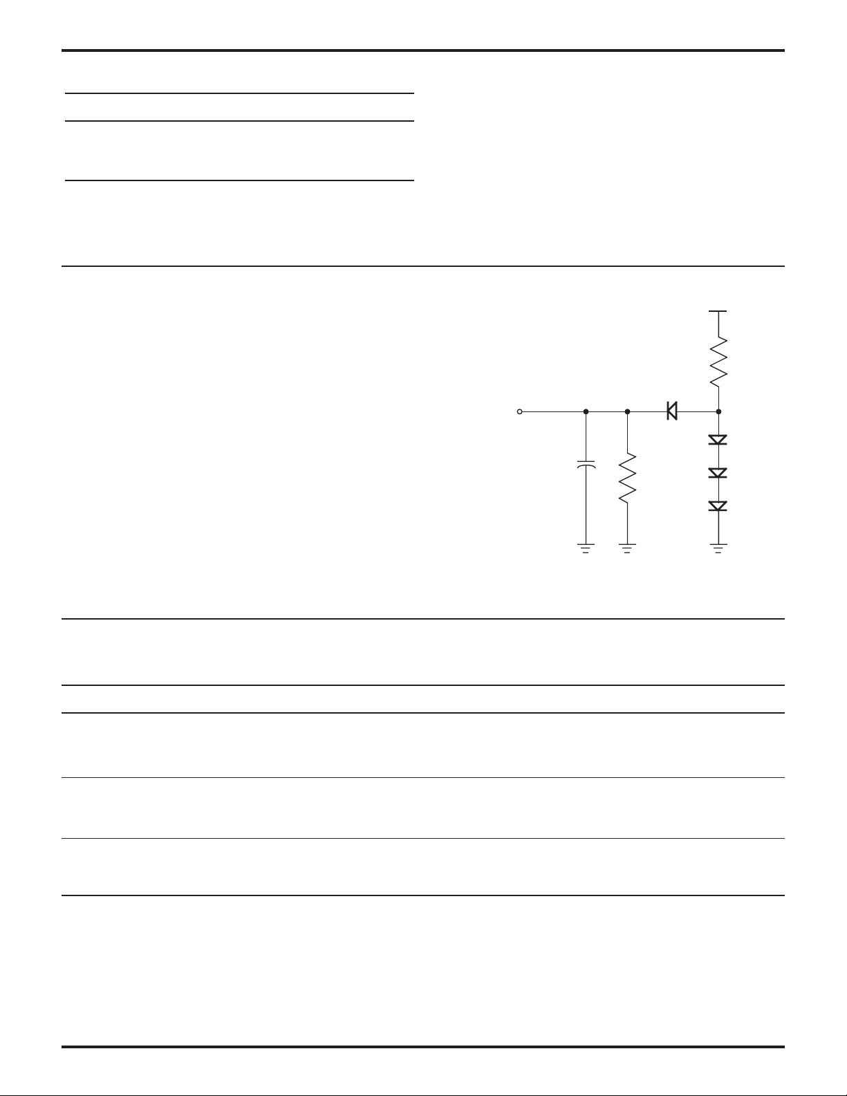
STANDARD TEST CONDITIONS
The characteristics listed below apply for standard test
conditions as noted. All voltages are referenced to ground.
Positive current flows into the referenced pin (Test Load).
Stresses greater than those listed under Absolute Maximum
Ratings may cause permanent damage to the device. This
is a stress rating only; operation of the device at any
condition above those indicated in the operational sections
of these specifications is not implied. Exposure to absolute
maximum rating conditions for extended period may affect
device reliability.
+5V
2.1 K Ω
From Output
Under Test
30 pF 9.1 K Ω
. Test Load Diagram
DC ELECTRICAL CHARACTERISTICS
(V
= 5V ±10%, TA = 0°C to +70°C unless otherwise specified)
DD
Symbol Parameter Condition Min. Max. Typical Units
I
DD
I
DC
V
IH
V
IL
IL Input Leakage 10 µA
V
OH
V
OL
I
FL
Supply Current V
= 5.25V 80 70 mA
DD
fclock = 20 MHz
DC Power Consumption V
= 5.25V 5 mA
DD
Input High Level 2.5 V
Input Low Level 0.8 V
Output High Voltage I
Output Low Voltage I
= –100 µAV
OH
= 2.0 mA 0.5 V
OL
– 0.2 V
DD
Output Floating Leakage Current 5 µA
4 DC 9030-00

ZILOG
PRELIMINARY
AC ELECTRICAL CHARACTERISTICS
(VDD = 5V 10%, T
Symbol Parameter Min (ns) Max (ns)
Clock
TCY Clock Cycle Time 50
Tr Clock Rise Time 2
Tf Clock Fall Time 2
CPW Clock Pulse Width 23
I/O
DSSET /DS Setup Time from CLOCK Fall 0 15
DSHOLD /DS Hold Time from CLOCK Rise 4 15
EASET EA Setup Time to /DS Fall 12
EAHOLD EA Hold Time from /DS Rise 4
RDSET Data Read Setup Time to /DS Rise 14
RDHOLD Data Read Hold Time from /DS Rise 6
WRSET Data Write Setup Time to /DS Rise 18
WRHOLD Data Write Hold Time from /DS Rise 5
Interrupt
INTSET Interrupt Setup Time to CLOCK Fall 7
INTWIDTH Interrupt Low Pulse Width 1 TCY
= 0°C to +70°C unless otherwise specified)
A
CPS DC-9030-01
Z89390
Codec Interface
SSET SCLK Setup Time from Clock Rise 15
FSSET FSYNC Setup Time from SCLK Rise 6
TXSET TXD Setup Time from SCLK Rise 7
RXSET RXD Setup Time to SCLK Fall 7
RXHOLD RXD Hold Time from SCLK Fall 0
Reset
RRISE Reset Rise Time 1000
RSET Reset Setup Time to CLOCK Rise 15
RWIDTH Interrupt Low Pulse Width 2 TCY
External Program Memory
PASET PA Setup Time from CLOCK Rise 5
PDSET PD Setup Time to CLOCK Rise 10
PDHOLD PD Hold Time from CLOCK Rise 10
Wait State
WSET WAIT Setup Time to CLOCK Rise 23
WHOLD WAIT Hold Time from CLOCK Rise 1
Halt
HSET Halt Setup Time to CLOCK Rise 3
HHOLD Halt Hold Time from CLOCK Rise 10
DC 9030-00 5

ZILOG
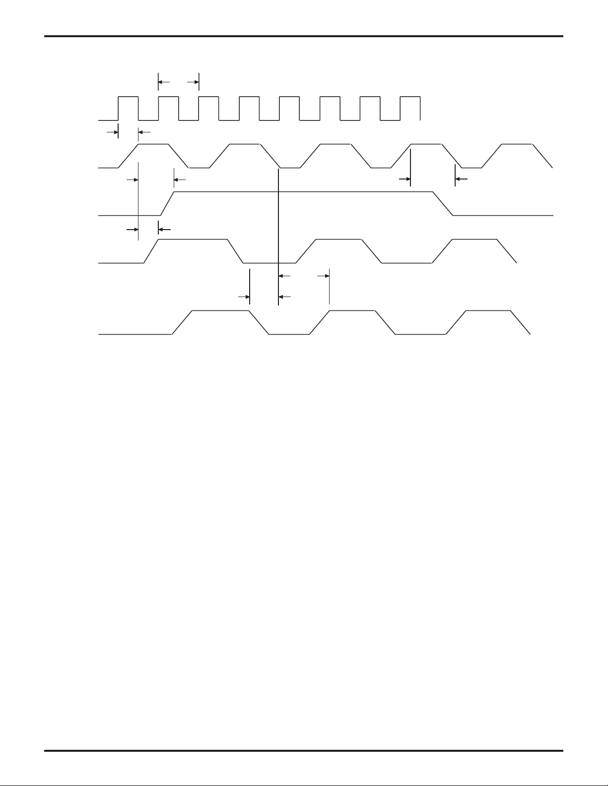
AC TIMING DIAGRAM
CLOCK
PRELIMINARY
TCY Tr Tf
CPS DC-9030-01
Z89390
/DS
EA(2:0)
RD//WR
EXT(15:0)
DSHOLD
DSSET
EASET EAHOLD
Valid Address Out
RDHOLD
RDSET
Data In
Read Timing Diagram
CPW
CLOCK
WAIT
/DS
EA(2:0)
RD//WR
EXT(15:0)
TCY
WHOLD
WSET
Valid Address Out
Data In
Read Timing Diagram Using WAIT Pin
6 DC 9030-00

ZILOG
CLOCK
/DS
PRELIMINARY
TCY
DSHOLD
DSSET
EASET EAHOLD
CPS DC-9030-01
Z89390
EA(2:0)
RD//WR
EXT(15:0)
CLOCK
WAIT
Valid Address Out
EASET
EAHOLD
WRHOLD
WRSET
Data In
Write Timing Diagram
TCY
WHOLD
WSET
/DS
EA(2:0)
RD//WR
EXT(15:0)
Valid Address Out
Data In
Write Timing Diagram Using WAIT Pin
DC 9030-00 7
ZILOG
AC TIMING (Continued)
CLOCK
SSET
SCLK
TCY
PRELIMINARY
CPS DC-9030-01
Z89390
FS0, FS1
TXD
RXD
FSSET
TXSET
RXHOLD
RXSET
1
01 0 1
Codec Interface Timing Diagram
FSSET
10101
8 DC 9030-00

ZILOG
AC TIMING (Continued)
CLOCK
INT 0,1,2
INTWidth
PRELIMINARY
TCY
INTSET
CPS DC-9030-01
Z89390
PROGRAM
ADDRESS
EXECUTE
CLOCK
HALT
Fetch N –1 Fetch N Fetch N +1 Fetch Int_Addr Fetch I Fetch I +1
Execute N –1 Execute N CALL Int Routine Execute Int Routine
Interrupt Timing Diagram
TCY
HHOLD
HSET
HALT Timing Diagram
DC 9030-00 9

ZILOG
AC TIMING (Continued)
CLOCK
RSET RRISE
/RESET
INTERNAL
RESET
RWIDTH
TCY
PRELIMINARY
CPS DC-9030-01
Z89390
EXECUTE
RD/WR
/DS
UO0-1
EA0-2
EXT0-15
PA0-15
RAM/
REGISTERS
Cycle 0
Cycle 1 Cycle 2 Cycle 3 Cycle 4 Cycle 5 Code Execution
Tri-Stated
Tri-Stated Access Reset Vector
Intact*
* The RAM and hardware registers are left intact
during a warm reset. A cold reset will produce
random data in these locations. The status
register is set to zeroes in both cases.
RESET Timing Diagram
TCY
CLOCK
PASET
PROGRAM
ADDRESS
PROGRAM
DATA
Valid Valid Valid
PDSET
PDHOLD
Valid
Valid
Valid
External Memory Port Timing Diagram
10 DC 9030-00

ZILOG
PRELIMINARY
CPS DC-9030-01
Z89390
© 1997 by Zilog, Inc. All rights reserved. No part of this document
may be copied or reproduced in any form or by any means
without the prior written consent of Zilog, Inc. The information in
this document is subject to change without notice. Devices sold
by Zilog, Inc. are covered by warranty and patent indemnification
provisions appearing in Zilog, Inc. Terms and Conditions of Sale
only. Zilog, Inc. makes no warranty, express, statutory, implied or
by description, regarding the information set forth herein or
regarding the freedom of the described devices from intellectual
property infringement. Zilog, Inc. makes no warranty of merchantability or fitness for any purpose. Zilog, Inc. shall not be
responsible for any errors that may appear in this document.
Zilog, Inc. makes no commitment to update or keep current the
information contained in this document.
Zilog’s products are not authorized for use as critical components in life support devices or systems unless a specific written
agreement pertaining to such intended use is executed between
the customer and Zilog prior to use. Life support devices or
systems are those which are intended for surgical implantation
into the body, or which sustains life whose failure to perform,
when properly used in accordance with instructions for use
provided in the labeling, can be reasonably expected to result in
significant injury to the user.
Zilog, Inc. 210 East Hacienda Ave.
Campbell, CA 95008-6600
Telephone (408) 370-8000
Telex 910-338-7621
FAX 408 370-8056
Internet: http://www.zilog.com
DC 9030-00 11
 Loading...