
DS97KEY0102
P R E L I M I N A R Y
1
1
P
RELIMINARY
P
RODUCT
S
PECIFICATION
Z86U18
1
USB D
EVICE
C
ONTROLLER
WITH
CMOS Z86K15 MCU
FEATURES
■
USB Serial Interface Engine, Transceiver, and MCU
Intergrated for USB Function Controller
■
+4.0V to +5.5V Operating Range
■
Low Power Consumption: 60 mW @ 6 MHz
■
Digital Inputs CMOS Levels with Internal Pull-Up
Resistors
■
Four Direct Connect LED Drive Ports
■
Power-On Reset (POR), Hardware Watch-Dog Timer
(WDT)
■
Intergrated USB Transceiver @ 1.5 Mb/sec
■
For Use In A Variety of Applications Including Keyboards
and Game Controllers
■
Programmable 8-Bit Counter/Timer, with 6-Bit
Programmable Prescaler
■
Five Vectored, Priority Interrupts from Five Different
Sources
■
On-Chip Oscillator, Which Accepts A Crystal, Ceramic
Resonator, LC or External Clock Drive (all clock speeds
@ 6 MHz)
■
Low System EMI Emission
■
HALT/STOP Modes
GENERAL DESCRIPTION
The Z86U18 USB Controller is a member of the Z8
¨
MCU
family. The Z86U18 is characterized by a flexible I/O
scheme, an efficient register architecture, and a number of
ancillary features. It contains a dedicated USB interface
(transceiver and SIE).
For applications demanding powerful I/O capabilities, the
Z86U18 (40- and 44-pin versions) provides 32 pins dedicated to application input and output. These lines are
grouped into four ports, each port consists of eight lines
and are configurable under software control to provide timing, status signals, and serial or parallel I/O ports. It also
has 2 pins to connect directly to the USB cable.
To unburden the system from coping with real-time tasks,
such as counting/timing and I/O data communications, the
Z86U18 offers an on-chip counter/timer with a large number of user-selectable modes.
The Z86U18 achieves low EMI by means of several circuit
implementations in the output drivers and clock circuitry of
the device.
With fast execution, efficient use of memory, sophisticated
interrupt, input/output bit-manipulation capabilities, and
easy hardware/software system expansion, along with low
cost and low power consumption, the Z86U18 meets the
needs of a variety of sophisticated applications (Figure 1:
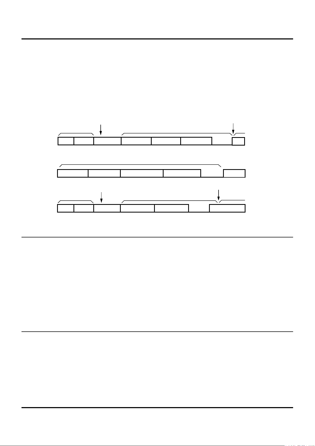
Functional Block Diagram)
Notes : All signals with a preceding front slash, "/", are ac-
tive Low. For example, B//W (WORD is active Low); /B/W
(BYTE is active Low, only).
Device
ROM
(KB)
RAM
(Bytes)
I/O
Lines
Speed
(MHz)
Z86U18 4 188 32 6
Z86U18
USB Device Controller with CMOS Z86K15 MCU Zilog
2
P R E L I M I N A R Y
DS97KEY0102
GENERAL DESCRIPTION (Continued)
Power connections follow conventional descriptions below:
This device is based on the Z86K15 device with the following changes or modifications:
1.
Power-On Reset (POR): POR timing is a function of
the system clock.
POR = (3
2
* 2
16
)/f = .098
POR is in seconds and frequency in Hz. It may need
a programmable timer for warm reset (USB reset).
2.
Watch-Dog Timer (WDT): WDT is also driven by the
system clock and subject to same tolerance. The
WDT can be programmed for time out value of:
WDT = POR/2
3. EMI, 801-2 and 801-4 Compliance : When used with
good engineering practice, this device should meet
Class B FCC with at least 10 dB of margin and comply
with the 801-2 group 4 air discharge. It shall meet 8014 EFT requirements in a system.
4. XTAL : Drive to 3-pin ceramic resonator (@ 6 MHz).
5.
XTAL In : From ceramic resonator or crystal.
Connection Circuit Device
Power V
CC
V
DD
Ground GND V
SS
Figure 1. Z86U18 Functional Block Diagram
Port 3
Interrupt
Control
Port 2
I/O
(Bit Programmable)
ALU
Flags
Register
Pointer
Machine
Timing & Inst.
Control
Program
Counter
GND
XTAL1
XTAL2
Output
Input
Port 0 Port 1
Open-Drain
Output
Open-Drain
Output
WDT
POR
Input
4
4
4
8 8
Counter/
Timers
USB SIE
and Trans
Register File
208 x 8-Bytes
Program
Memory
4 KB ROM
VCC
D+
D-
3.3 V
VR
VCC
V
USB
Z86U18
Zilog USB Device Controller with CMOS Z86K15 MCU
DS97KEY0102
P R E L I M I N A R Y
3
1
USB FUNCTIONAL BLOCK DESCRIPTION
The USB portion of the chip is divided into two areas, the
transceiver and the Serial Interface Engine (SIE). The
transceiver handles incoming differential signals and "single ended zero" (SE0). It also converts output data in digital form to differential drive at the proper levels.
The SIE does all other processing on incoming and out going data. This includes signal recovery timing, bit stuffing,
validity checking, data sequencing, and handshaking to
the host. Data flow into and out of the MCU portions is processed through eight registers mapped into Expanded
Register File Memory at locations 010 to 017.
The USB SIE handles two endpoints (control at Endpoint
0 and data into the host from Endpoint 1). All communications are at the 1.5 Mb/sec HID class data rate. Future devices will handle the full 12 Mb/sec data rate.
USB SUSPEND/RESUME FUNCTIONALITY
Suspend is intitiated by the host only, when it stops sending start of frame signaling or start of frame keep alive
pulse.
When SIE detects the absence of start of frame signaling
from the host for more than 3 miliseconds, it sets the Suspend bit in Reg7 and the Supspend Interrupt bit in Reg6
which interrupts the microcontroller. There is also an internal Suspend node that reflects the state of the Suspend bit
in Reg7. This Suspend node is used to put the tranceiver
in Suspend mode. When the microcontroller gets the Suspend Interrupt, it stops all the clocks.
Resume can be initiated by host or by UC. Host initiates
Resume by sending J to K transition on D+ and D- pins.
Upon detecting J to K transition, the GFI makes Resumeout signal active, which is used to wake the UC. Once the
UC is up, it clears the suspend bit in Reg7. UC can initiate
Resume by writing 1 to Send Resume bit in Reg7 for longer than 10mSec. This makes GFI to send J to K transition
on D+ and D- pins which indicates to the host the Resume
state. After 10 msec UC also clears the Suspend bit in
Reg7.
U18 EMULATIONS AND CODE DEVELOPMENT
An existing ICEBOXª Emulator has been modified by the
addition of an adaptor board. This board includes a FPGA
with the logic of the SIE, a commercial USB transceiver,
and a voltage regulator. These three functions adapt our
Z86C15/K15 to the USB world allowing the customer to
develop code to be placed into the ROM of U18s.
The ICEBOX has complete functional equivalence to the
final part including pin out to the application board. This
begins with the 40-pin DIP and covers the other pin configurations. Once code has been verified, it can be released
to Zilog and placed into the ROM of the Z86U18.
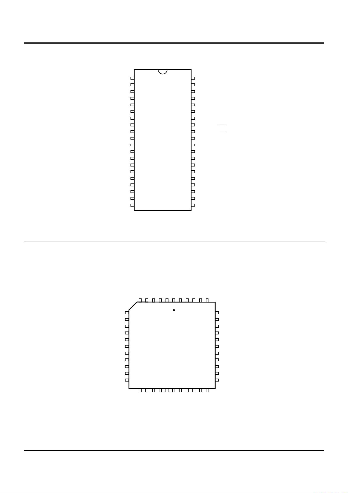
Figure 2. Data To/From K86U18
SYNC DATA CRC EOP
Data packet sent at low speed
SYNC
SYNC
Hub Setup
ENDP . . .
EOP
Hub enables low
speed port outputs
Hub enables low
speed port outputs
Preamble
sent at full speed Token sent at low speed
SYNCSYNC Hub Setup EOP
Preamble
sent at full speed
Hub enables low
speed port outputs Handshake sent at low speed
Hub enables low
speed port outputs
PID
PID
PID
PID
PID
Z86U18
USB Device Controller with CMOS Z86K15 MCU Zilog
4
P R E L I M I N A R Y
DS97KEY0102
PIN IDENTIFICATION
Figure 3. 40-Pin DIP Pin ConÞguration
P36
P17
P16
P15
P14
P13
P12
P11
P10
P35
GND
P00
P01
P02
P03
P04
P05
P06
P07
P34
P23
P22
P21
P20
P37
P24
Test
XTALI (IN)
XTAL0
GND
P25
P26
VUSB
V
CC
D+
DP30
P31
P32
P33
40
Z86UXX
DIP
1
20 21
2
3
4
5
6
7
8
9
10
11
12
13
14
15
16
17
18
19
39
38
37
36
35
34
33
32
31
30
29
28
27
26
25
24
23
22
(OUT)
Pin assignments to be determined.
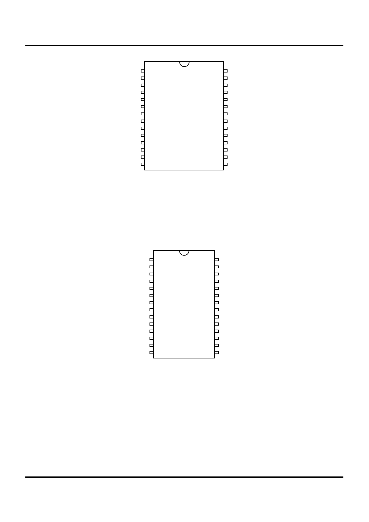
Figure 4. 44-Pin PLCC and QFP Pin Assignments
Z86U18
PLCC/QFP
7
8
9
10
11
12
13
14
15
16
17
XXX
XXX
XXX
XXX
XXX
XXX
XXX
XXX
XXX
XXX
XXX
XXX
XXX
XXX
XXX
XXX
XXX
XXX
XXX
XXX
XXX
XXX
XXX
XXX
XXX
XXX
XXX
XXX
XXX
XXX
XXX
XXX
XXX
XXX
XXX
XXX
XXX
XXX
XXX
XXX
XXX
XXX
XXX
XXX
1
2818
406
39
38
37
36
35
34
33
32
31
30
29
20 22 24 26
4
42
Z86U18
Zilog USB Device Controller with CMOS Z86K15 MCU
DS97KEY0102
P R E L I M I N A R Y
5
1
Pin assignments to be determined.
Figure 5. 28-pin SOIC Assignments
XXX
XXX
XXX
XXX
XXX
XXX
XXX
XXX
XXX
XXX
XXX
XXX
XXX
XXX
XXX
XXX
XXX
XXX
XXX
XXX
XXX
XXX
XXX
XXX
XXX
XXX
XXX
XXX
28
Z86U18
SOIC
1
14 15
Pin assignments to be determined.
Figure 6. 28-pin PDIP Assignments
XXX
XXX
XXX
XXX
XXX
XXX
XXX
XXX
XXX
XXX
XXX
XXX
XXX
XXX
XXX
XXX
XXX
XXX
XXX
XXX
XXX
XXX
XXX
XXX
XXX
XXX
XXX
XXX
28
Z86U18
PDIP
1
14 15
Z86U18
USB Device Controller with CMOS Z86K15 MCU Zilog
6
P R E L I M I N A R Y
DS97KEY0102
ABSOLUTE MAXIMUM RATINGS
Stresses greater than those listed under Absolute Maximum Ratings may cause permanent damage to the device. This is a stress rating only; operation of the device at
any condition above those indicated in the operational sections of these specifications is not implied. Exposure to absolute maximum rating conditions for extended periods
may affect device reliability.
STANDARD TEST CONDITIONS
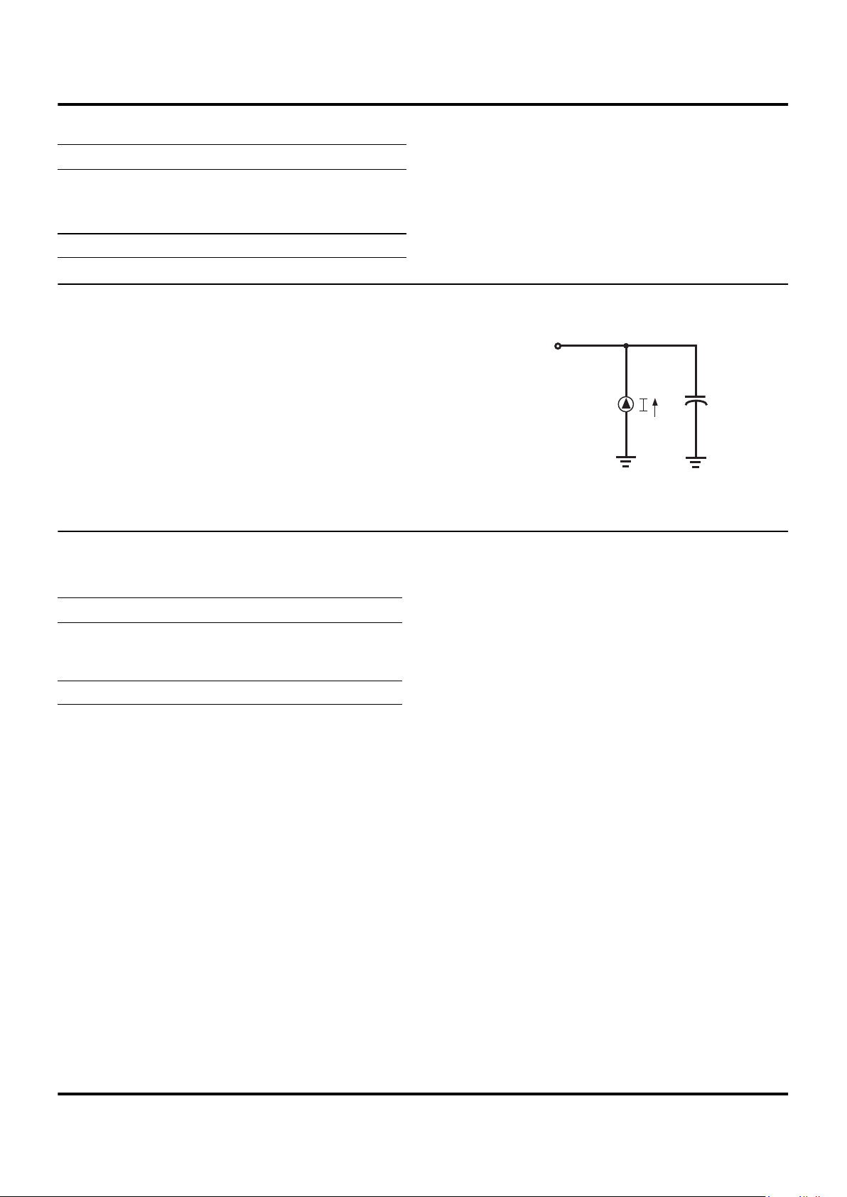
The characteristics listed here apply for standard test conditions as noted. All voltages are referenced to GND. Positive current flows into the referenced pin (Figure 7).
CAPACITANCE
T
A
= 25 ° C; V
CC
= GND = 0V; f = 1.0 MHz; unmeasured pins returned to GND.
Symbol Description Min Max Units
V
CC
Supply Voltage* Ð0.3 +7.0 V
T
STG
Storage Temp Ð65 +150 ° C
T
A
Oper Ambient Temp 0 +105 ° C
Note: * Voltage on all pins with respect to GND.
Figure 7. Test Load Diagram
From Output
Under Test
150 pF
Parameter Max
Input Capacitance 12 pF
Output Capacitance 12 pF
I/O Capacitance 12 pF
Note: Frequency tolerance ± 10%

Z86U18
Zilog USB Device Controller with CMOS Z86K15 MCU
DS97KEY0102
P R E L I M I N A R Y
7
1
DC CHARACTERISTICS
V
CC
= 4.0V to 5.5V @ 0 ° C to +70 ° C
Sym Parameter Min Max Unit Condition
V
CH
Clock Input High Voltage 0.7 V
CC
V
CC
+ 0.3V V Driven by External Clock Generator
V
CL
Clock Input Low Voltage GND Ð0.3 0.2 V
CC
V Driven by External Clock Generator
V
IH
Input High Voltage 0.7 V
CC
V
CC
+ 0.3 V
V
IL
Input Low Voltage GND Ð0.3 0.2 V
CC
V
V
OH
Output High Voltage VCC Ð0.4 V IOH = Ð2.0 mA
V
OH
Output High Voltage VCC Ð0.6 V I
OH
= Ð2.0 mA (see note 1 below.)
V
OL
Output Low Voltage .4 V IOL= 4 mA
V
OL
Output Low Voltage .8 V IOL= 4 mA (see note 1 below.)
I
OL
Output Low 10 20 mA VOL= VCC Ð2.2 V (see note 1 below.)
I
OL
Output Leakage Ð1 1 mAVIN = 0V, 5.25V
I
CC
VCC Supply Current 12 mA @ 6.0 MHz
I
CC1
Halt Mode Current TBD mA @ 6.0 MHz
I
CC2
Stop Mode Current 10 mA
R
p
Pull Up Resistor 6.76 14.04 K ohm
R
p
Pull Up Resistor (P26-P25) 1.8 3 K ohm
VUSB Voltage Regulator Output 3.0 3.6 V
D+,D- Differential Signaling D- > D+ D+ > D- mV @ > 200mV Difference (see note 2
below)
Notes:
1. Ports P37-P34. These may be used for LEDs or as general-purpose outputs requiring high sink current.
2. Except for SE0 for EOP and RESET (See 7.1.4 of USB Specification).
Z86U18
USB Device Controller with CMOS Z86K15 MCU Zilog
8 P R E L I M I N A R Y DS97KEY0102
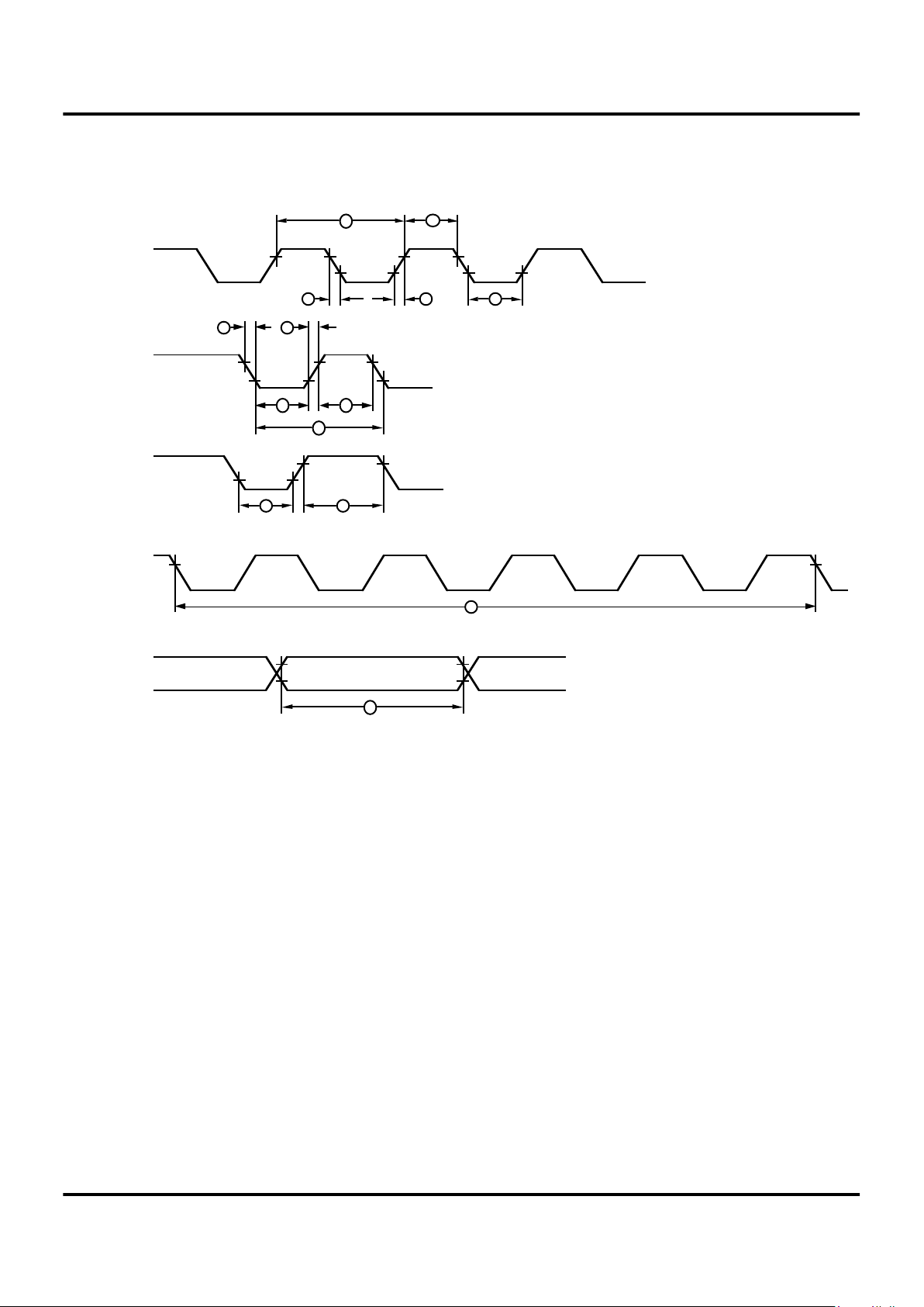
AC ELECTRICAL CHARACTERISTICS
Additional Timing Diagram
Figure 8. Additional Timing
Clock
1
3
4
8
223
TIN
IRQN
6
5
7
7
1
1
Clock
Setup
1
0
9
S
top
Mode
Recovery
Source

Z86U18
Zilog USB Device Controller with CMOS Z86K15 MCU
DS97KEY0102 P R E L I M I N A R Y 9
1
AC ELECTRICAL CHARACTERISTICS
Additional Timing Table
T
A
=0°C to +70°C
5.0V, 6 MHz
No Symbol Parameter Min Max Units Notes
1 TpC Input Clock Period 150 250 ns 1
2 TrC,TfC Clock Input Rise & Fall Times 25 ns 1
3 TwC Input Clock Width 37 ns 1
4 TwTinL Timer Input Low Width 70 ns 1
5 TwTinH Timer Input High Width 2.5TpC 1
6 TpTin Timer Input Period 4TpC 1
7 TrTin Timer Input Rise & Fall Timer 100 ns 1
8 TwIL Int. Request Low Time 70 ns 1,2
9 TwIH Int. Request Input High Time 3TpC 1,2
10 Twsm Stop-Mode Recovery Width Spec 5TpC ns
11 Tost Oscillator Start-up Time 5TpC ns
12 Twdt Watch-Dog Timer 3,0 ms
13 D+, D- Differential Rise and Fall Times 70 300 nS 3
Notes:
1. Timing Reference uses 0.7 V
CC
for a logic 1 and 0.2 VCC for a logic 0.
2. Interrupt request through Port 3 (P33-P31)
3. See USB Specification 7.1.1.2
 Loading...