


1
Z8
P
RELIMINARY
P
RODUCT
S
PECIFICATION
FEATURES
ROM
Device
Z86E30 4 237 24 16
Z86E31 2 125 24 16
Z86E40 4 236 32 16
Note: *General-Purpose
■
Standard Temperature (V
■
Extended Temperature (V
■
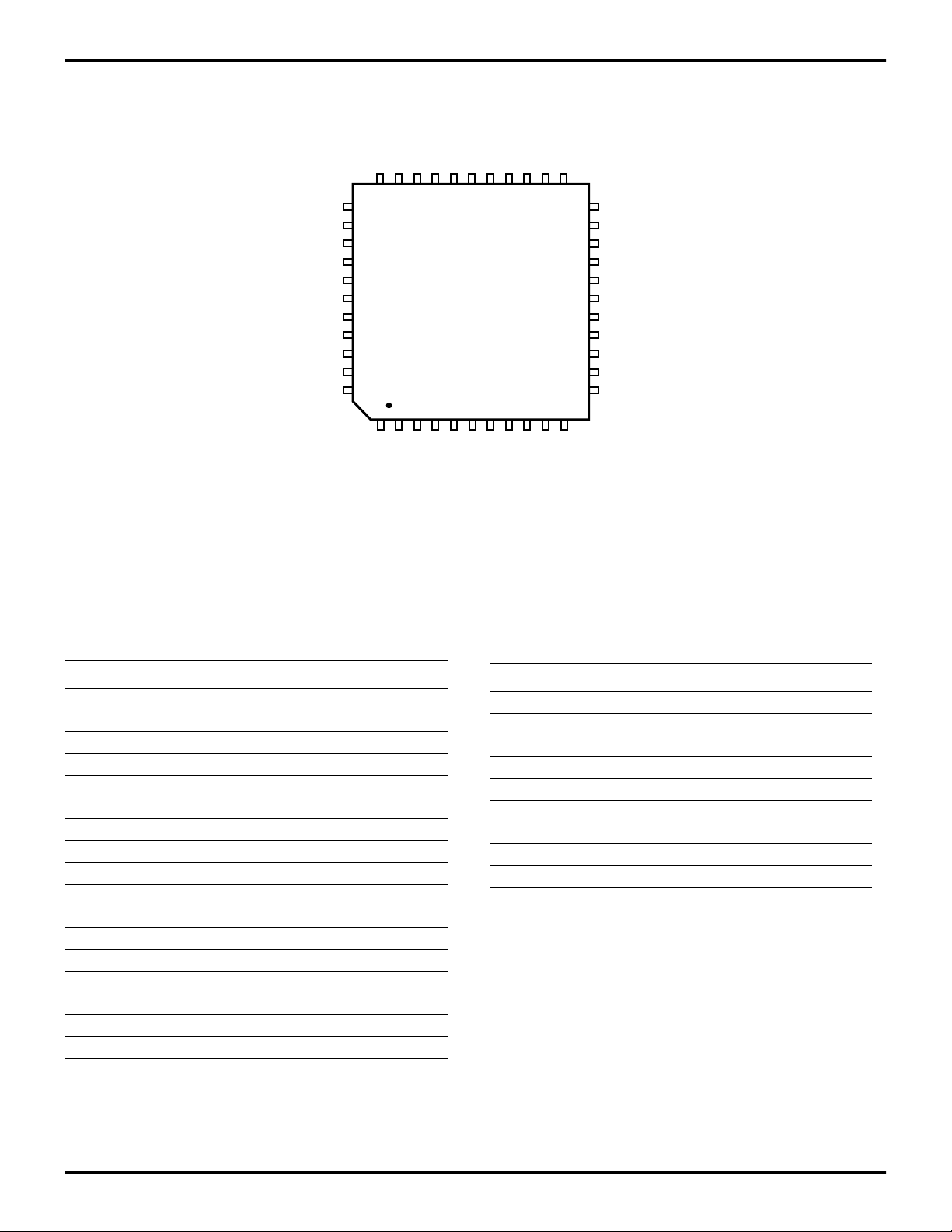
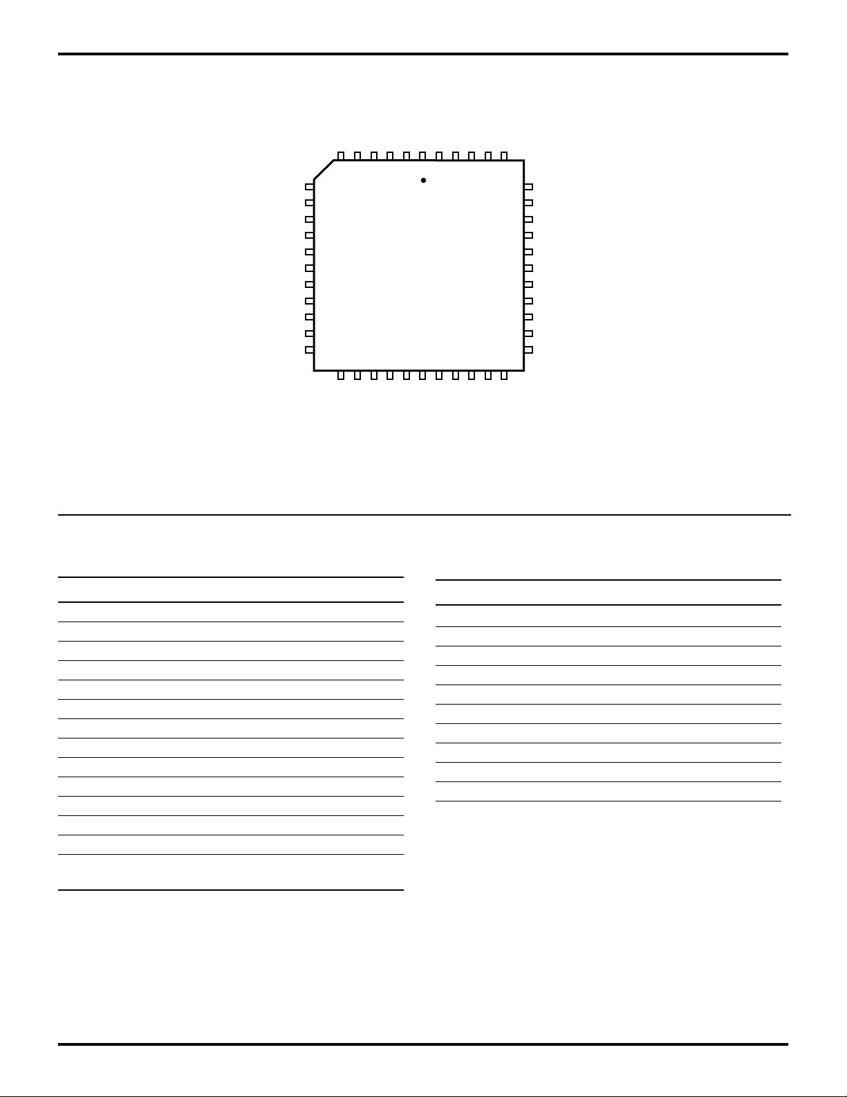
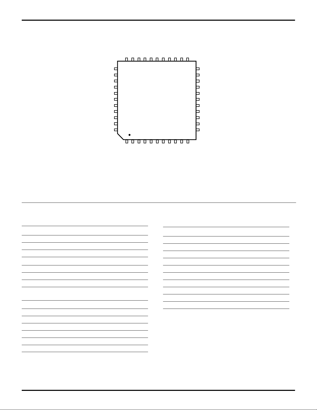
Available Packages:
28-Pin DIP/SOIC/PLCC OTP (Z86E30/31 only)
28-Pin DIP Window (Z86E30/31 only)
40-Pin DIP OTP/Window (Z86E40 only)
44-Pin PLCC/QFP OTP (Z86E40 only)
44-Pin PLCC Window (Z86E40 only)
■
Software Enabled Watch-Dog Timer (WDT)
■
Push-Pull/Open-Drain Programmable on
Port 0, Port 1, and Port 2
■
24/32 Input/Output Lines
■
Auto Latches
(KB)
RAM*
(Bytes)
= 3.5V to 5.5V)
CC
= 4.5V to 5.5V)
CC
I/O
Lines
Speed
(MHz)
Z86E30/E31/E40
4K OTP M
■
Programmable OTP Options:
RC Oscillator
EPROM Protect
Auto Latch Disable
Permanently Enabled WDT
Crystal Oscillator Feedback Resistor Disable
RAM Protect
■
Low-Power Consumption: 60 mW
Fast Instruction Pointer: 0.75 µ s
■
■
Two Standby Modes: STOP and HALT
■
Digital Inputs CMOS Levels, Schmitt-Triggered
■
Software Programmable Low EMI Mode
■
Two Programmable 8-Bit Counter/Timers Each
with a 6-Bit Programmable Prescaler
■
Six Vectored, Priority Interrupts from Six
Different Sources
■
Two Comparators
■
On-Chip Oscillator that Accepts a Crystal, Ceramic
Resonator, LC, RC, or External Clock Drive
ICROCONTROLLER
1
■
Auto Power-On Reset (POR)
GENERAL DESCRIPTION
The Z86E30/E31/E40 8-Bit One-Time Programmable
(OTP) Microcontrollers are members of Zilog's single-chip
®
Z8
MCU family featuring enhanced wake-up circuitry,
programmable Watch-Dog Timers, Low Noise EMI options, and easy hardware/software system expansion capability.
Four basic address spaces support a wide range of memory configurations. The designer has access to three addi-
DS97Z8X0500
P R E L I M I N A R Y
tional control registers that allow easy access to register
mapped peripheral and I/O circuits.
For applications demanding powerful I/O capabilities, the
Z86E30/E31 have 24 pins, and the Z86E40 has 32 pins of
dedicated input and output. These lines are grouped into
four ports, eight lines per port, and are configurable under
software control to provide timing, status signals, and par-
1
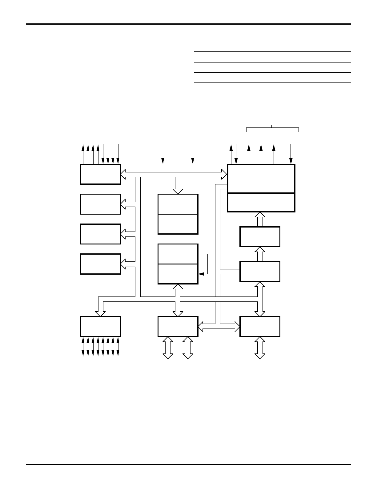
2
Z86E30/E31/E40
Z8 4K OTP Microcontroller Zilog
allel I/O with or without handshake, and address/data bus
for interfacing external memory.
Notes: All Signals with a preceding front slash, "/", are
active Low, for example, B//W (WORD is active Low); /B/W
(BYTE is active Low, only).
Output Input
Port 3
Counter/
Timers (2)
VCC
ALU
Power connections follow conventional descriptions below:
Connection Circuit Device
GND
Power V
CC
Ground GND V
(E40 Only)
XTAL
/AS /DS R//W /RESET
Machine Timing
&
Instruction Control
RESET
WDT, POR
V
DD
SS
Interrupt
Control
T wo Analog
Comparators
Port 2
I/O
(Bit Programmable)
Figure 1. Z86E30/E31/E40 Functional Block Diagram
FLAGS
Register
Pointer
Register File
Port 0
44
Address or I/O
(Nibble Programmable)
OTP
Program
Counter
Port 1
8
Address/Data or I/O
(Byte Programmable)
(E40 Only)
P R E L I M I N A R Y
DS97Z8X0500
1
Zilog Z8 4K OTP Microcontroller
D7 - 0
AD 11- 0
Z8 MCU
AD 11- 0
Z86E30/E31/E40
MSN
Port 3
Z8
Port 0
AD 11- 0
PGM + Test
Mode Logic
EPM
P32
/CE
XT1
/PGM
P30
Address
MUX
EPROM
TEST ROM
OTP
Options
VPP
P33
D7 - 0
Data
MUX
D7 - 0
Z8
Port 2
/OE
P31
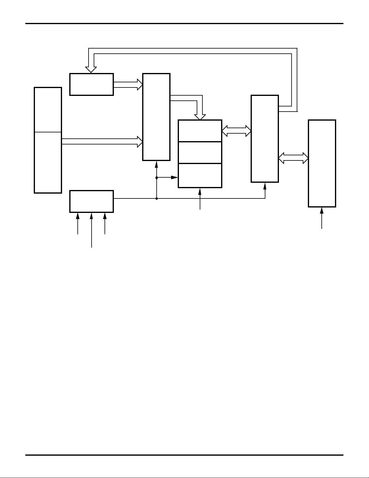
Figure 2. EPROM Programming Block Diagram
DS97Z8X0500
P R E L I M I N A R Y
3
4
Z86E30/E31/E40
Z8 4K OTP Microcontroller Zilog
PIN IDENTIFICATION
Table 1. 40-Pin DIP Pin Identification
Standard Mode
R//W
P25
P26
P27
P04
P05
P06
P14
P15
P07
VCC
P16
P17
XTAL2
XTAL1
P31
P32
P33
P34
/AS
1
40-Pin DIP
20 21
Figure 3. 40-Pin DIP Pin Configuration*
Standard Mode
40
/DS
P24
P23
P22
P21
P20
P03
P13
P12
GND
P02
P11
P10
P01
P00
P30
P36
P37
P35
/RESET
Pin # Symbol Function Direction
1 R//W Read/Write Output
2-4 P25-P27 Port 2, Pins 5,6,7 In/Output
5-7 P04-P06 Port 0, Pins 4,5,6 In/Output
8-9 P14-P15 Port 1, Pins 4,5 In/Output
10 P07 Port 0, Pin 7 In/Output
11 V
CC
Power Supply
12-13 P16-P17 Port 1, Pins 6,7 In/Output
14 XTAL2 Crystal Oscillator Output
15 XTAL1 Crystal Oscillator Input
16-18 P31-P33 Port 3, Pins 1,2,3 Input
19 P34 Port 3, Pin 4 Output
20 /AS Address Strobe Output
21 /RESET Reset Input
22 P35 Port 3, Pin 5 Output
23 P37 Port 3, Pin 7 Output
24 P36 Port 3, Pin 6 Output
25 P30 Port 3, Pin 0 Input
26-27 P00-P01 Port 0, Pins 0,1 In/Output
28-29 P10-P11 Port 1, Pins 0,1 In/Output
30 P02 Port 0, Pin 2 In/Output
31 GND Ground
32-33 P12-P13 Port 1, Pins 2,3 In/Output
34 P03 Port 0, Pin 3 In/Output
35-39 P20-P24 Port 2, Pins
In/Output
0,1,2,3,4
40 /DS Data Strobe Output
Notes:
*Pin Configuration and Identification identical on DIP
and Cerdip Window Lid style packages.
P R E L I M I N A R Y
DS97Z8X0500
1
Z86E30/E31/E40
Zilog Z8 4K OTP Microcontroller
P20
P03
P13
P12
GND
GND
P02
P11
P10
P01
P21
P22
P23
P24
/DS
NC
R//W
P25
P26
P27
P04
7
17
6
P05
P06
P14
1
44-Pin PLCC
P15
P07
VCC
P16
VCC
2818
P17
XTAL2
Figure 4. 44-Pin PLCC Pin Configuration
Standard Mode
40
29
P00
39
XTAL1
P30
P36
P37
P35
/RESET
R//RL
/AS
P34
P33
P32
P31
Table 2. 44-Pin PLCC Pin Identification
Pin # Symbol Function Direction
1-2 GND Ground
3-4 P12-P13 Port 1, Pins 2,3 In/Output
5 P03 Port 0, Pin 3 In/Output
6-10 P20-P24 Port 2, Pins
In/Output
0,1,2,3,4
11 /DS Data Strobe Output
12 NC No Connection
13 R//W Read/Write Output
14-16 P25-P27 Port 2, Pins 5,6,7In/Output
17-19 P04-P06 Port 0, Pins 4,5,6In/Output
20-21 P14-P15 Port 1, Pins 4,5 In/Output
22 P07 Port 0, Pin 7 In/Output
23-24 VCC Power Supply
25-26 P16-P17 Port 1, Pins 6,7 In/Output
27 XTAL2 Crystal OscillatorOutput
28 XTAL1 Crystal OscillatorInput
29-31 P31-P33 Port 3, Pins 1,2,3Input
32 P34 Port 3, Pin 4 Output
Table 2. 44-Pin PLCC Pin Identification
Pin # Symbol Function Direction
33 /AS Address Strobe Output
34 R//RL ROM/ROMless
Input
select
35 /RESET Reset Input
36 P35 Port 3, Pin 5 Output
37 P37 Port 3, Pin 7 Output
38 P36 Port 3, Pin 6 Output
39 P30 Port 3, Pin 0 Input
40-41 P00-P01 Port 0, Pins 0,1 In/Output
42-43 P10-P11 Port 1, Pins 0,1 In/Output
44 P02 Port 0, Pin 2 In/Output
DS97Z8X0500
P R E L I M I N A R Y
5
6
Z86E30/E31/E40
Z8 4K OTP Microcontroller Zilog
P20
P03
P13
P12
GND
GND
P02
P11
P10
P01
P00
2333
P17
12
11
XTAL2
22
XTAL1
P30
P36
P37
P35
/RESET
R//RL
/AS
P34
P33
P32
P31
P21
P22
P23
P24
/DS
NC
R//W
P25
P26
P27
P04
34
44
1
P05
P06
44-Pin QFP
P14
P15
P07
VCC
VCC
P16
Figure 5. 44-Pin QFP Pin Configuration
Table 3. 44-Pin QFP Pin Identification
Pin # Symbol Function Direction
1-2 P05-P06 Port 0, Pins 5,6 In/Output
3-4 P14-P15 Port 1, Pins 4,5 In/Output
5 P07 Port 0, Pin 7 In/Output
6-7 VCC Power Supply
8-9 P16-P17 Port 1, Pins 6,7 In/Output
10 XTAL2 Crystal Oscillator Output
11 XTAL1 Crystal Oscillator Input
12-14 P31-P13 Port 3, Pins 1,2,3 Input
15 P34 Port 3, Pin 4 Output
16 /AS Address Strobe Output
17 R//RL ROM/ROMless select Input
18 /RESET Reset Input
19 P35 Port 3, Pin 5 Output
20 P37 Port 3, Pin 7 Output
21 P36 Port 3, Pin 6 Output
22 P30 Port 3, Pin 0 Input
23-24 P00-P01 Port 0, Pin 0,1 In/Output
25-26 P10-P11 Port 1, Pins 0,1 In/Output
Standard Mode
Table 3. 44-Pin QFP Pin Identification
Pin # Symbol Function Direction
27 P02 Port 0, Pin 2 In/Output
28-29 GND Ground
30-31 P12-P13 Port 1, Pins 2,3 In/Output
32 P03 Port 0, Pin 3 In/Output
33-37 P20-4 Port 2, Pins 0,1,2,3,4 In/Output
38 /DS Data Strobe Output
39 NC No Connection
40 R//W Read/Write Output
41-43 P25-P27 Port 2, Pins 5,6,7 In/Output
44 P04 Port 0, Pin 4 In/Output
P R E L I M I N A R Y
DS97Z8X0500
1
Z86E30/E31/E40
Zilog Z8 4K OTP Microcontroller
Table 4. 40-Pin DIP Package Pin Identification
EPROM Mode
NC
D5
D6
D7
A4
A5
A6
NC
NC
A7
VCC
NC
NC
NC
/CE
/OE
EPM
VPP
A8
NC
1
40-Pin DIP
20 21
40
NC
D4
D3
D2
D1
D0
A3
NC
NC
GND
A2
NC
NC
A1
A0
/PGM
A10
A11
A9
NC
Pin # Symbol Function Direction
1 NC No Connection
2-4 D5-D7 Data 5,6,7 In/Output
5-7 A4-A6 Address 4,5,6 Input
8-9 NC No Connection
10 A7 Address 7 Input
11 V
CC
Power Supply
12-14 NC No Connection
15 /CE Chip Select Input
16 /OE Output Enable Input
17 EPM EPROM Prog. Mode Input
18 VPP Prog. Voltage Input
19 A8 Address 8 Input
20-21 NC No Connection
22 A9 Address 9 Input
23 A11 Address 11 Input
24 A10 Address 10 Input
25 /PGM Prog. Mode Input
Figure 6. 40-Pin DIP Pin Configuration*
EPROM Mode
26-27 A0-A1 Address 0,1 Input
28-29 NC No Connection
30 A2 Address 2 Input
31 GND Ground
32-33 NC No Connection
34 A3 Address 3 Input
35-39 D0-D4 Data 0,1,2,3,4 In/Output
40 NC No Connection
Note:
*Pin Configuration and Description identical on DIP and Cerdip
Window Lid style packages.
DS97Z8X0500
P R E L I M I N A R Y
7
8
Z86E30/E31/E40
Z8 4K OTP Microcontroller Zilog
D1
D2
D3
D4
NC
NC
NC
D5
D6
D7
A4
D0A3NCNCGND
6
7
17
A5
A6
NC
44 -Pin PLCC
GNDA2NCNCA1
1
A7
NC
VCC
NCNCNC
VCC
A0
40
39
29
2818
/CE
Figure 7. 44-Pin PLCC Pin Configuration
EPROM Programming Mode
/PGM
A10
A11
A9
NC
NC
NC
A8
VPP
EPM
/OE
Table 5. 44-Pin PLCC Pin Configuration
EPROM Programming Mode
Pin # Symbol Function Direction
1-2 GND Ground
3-4 NC No Connection
5 A3 Address 3 Input
6-10 D0-D4 Data 0,1,2,3,4 In/Output
11-13 NC No Connection
14-16 D5-D7 Data 5,6,7 In/Output
17-19 A4-A6 Address 4,5,6 Input
20-21 NC No Connection
22 A7 Address 7 Input
23-24 VCC Power Supply
25-27 NC No Connection
28 /CE Chip Select Input
29 /OE Output Enable Input
30 EPM EPROM Prog.
Input
Mode
Table 5. 44-Pin PLCC Pin Configuration
EPROM Programming Mode
Pin # Symbol Function Direction
31 V
PP
Prog. Voltage Input
32 A8 Address 8 Input
33-35 NC No Connection
36 A9 Address 9 Input
37 A11 Address 11 Input
38 A10 Address 10 Input
39 /PGM Prog. Mode Input
40-41 A0,A1 Address 0,1 Input
42-43 NC No Connection
44 A2 Address 2 Input
P R E L I M I N A R Y
DS97Z8X0500
1
Z86E30/E31/E40
Zilog Z8 4K OTP Microcontroller
D1
D2
D3
D4
NC
NC
NC
D5
D6
D7
A4
D0A3NCNCGND
34
44
1
A5
A6
NCNCNC
44 -Pin QFP
GNDA2NCNCA1
A7
VCC
VCC
NC
NC
2333
12
11
Figure 8. 44-Pin QFP Pin Configuration
EPROM Programming Mode
A0
22
/CE
/PGM
A10
A11
A9
NC
NC
NC
A8
VPP
EPM
/OE
Table 6. 44-Pin QFP Pin Identification
EPROM Programming Mode
Pin # Symbol Function Direction
1-2 A5-A6 Address 5,6 Input
3-4 NC No Connection
5 A7 Address 7 Input
6-7 V
CC
Power Supply
8-10 NC No Connection
11 /CE Chip Select Input
12 /OE Output Enable Input
13 EPM EPROM Prog.
Input
Mode
14 V
PP
Prog. Voltage Input
15 A8 Address 8 Input
16-18 NC No Connection
19 A9 Address 9 Input
20 A11 Address 11 Input
21 A10 Address 10 Input
22 /PGM Prog. Mode Input
Table 6. 44-Pin QFP Pin Identification
EPROM Programming Mode
Pin # Symbol Function Direction
23-24 A0,A1 Address 0,1 Input
25-26 NC No Connection
27 A2 Address 2 Input
28-29 GND Ground
30-31 NC No Connection
32 A3 Address 3 Input
33-37 D0-D4 Data 0,1,2,3,4 In/Output
38-40 NC No Connection
41-43 D5-D7 Data 5,6,7 In/Output
44 A4 Address 4 Input
DS97Z8X0500
P R E L I M I N A R Y
9
25
19
5
11
18
12
264
28-Pin PLCC
1
XXX
XXX
XXX
XXX
XXX
XXX
XXX
XXX
XXX
XXX
XXX
XXX
XXX
XXX
P21
P20
P03
VSS
P02
P01
P00
P05
P06
P07
VCC
XT2
XT1
P31
P04
P27
P26
P25
P24
P23
P22
P32
P33
P34
P35
P37
P36
P30
10
Z86E30/E31/E40
Z8 4K OTP Microcontroller Zilog
P25
P26
P27
P04
P05
P06
P07
VCC
XTAL2
XTAL1
P31
P32
P33
P34
1
28-Pin DIP
14 15
28
P24
P23
P22
P21
P20
P03
VSS
P02
P01
P00
P30
P36
P37
P35
Figure 9. Standard Mode
28-Pin DIP/SOIC Pin Configuration*
Table 7. 28-Pin DIP/SOIC/PLCC
Pin Identification*
Pin # Symbol Function Direction
1-3 P25-P27 Port 2, Pins 5,6, In/Output
4-7 P04-P07 Port 0, Pins 4,5,6,7 In/Output
8V
CC
Power Supply
9 XTAL2 Crystal Oscillator Output
10 XTAL1 Crystal Oscillator Input
11-13 P31-P33 Port 3, Pins 1,2,3 Input
14-15 P34-P35 Port 3, Pins 4,5 Output
16 P37 Port 3, Pin 7 Output
17 P36 Port 3, Pin 6 Output
18 P30 Port 3, Pin 0 Input
19-21 P00-P02 Port 0, Pins 0,1,2 In/Output
22 V
SS
Ground
23 P03 Port 0, Pin 3 In/Output
24-28 P20-P24 Port 2, Pins
0,1,2,3,4
Notes:
*Pin Identification and Configuration identical on DIP and
Cerdip Window Lid style packages.
In/Output
D5
D6
D7
A4
A5
A6
A7
VCC
NC
/CE
/OE
EPM
VPP
A8
1
28-Pin DIP
14 15
28
D4
D3
D2
D1
D0
A3
VSS
A2
A1
A0
/PGM
A10
A11
A9
Figure 10. EPROM Programming Mode
28-Pin DIP/SOIC Pin Configuration*
Figure 11. Standard Mode
28-Pin PLCC Pin Configuration
P R E L I M I N A R Y
DS97Z8X0500
Z86E30/E31/E40
1
Zilog Z8 4K OTP Microcontroller
Table 8. 28-Pin EPROM
Pin Identification*
Pin # Symbol Function Direction
1-3 D5-D7 Data 5,6,7 In/Output
4-7 A4-A7 Address 4,5,6,7 Input
8VCCPower Supply
9 NC No connection
10 /CE Chip Select Input
11 /OE Output Enable Input
12 EPM EPROM Prog.
Input
Mode
13 V
PP
Prog. Voltage Input
14-15 A8-A9 Address 8,9 Input
16 A11 Address 11 Input
17 A10 Address 10 Input
XXX
A5
XXX
A6
XXX
A7
XXX
VCC
XXX
NC
XXX
/CE
XXX
/OE
A4D7D6D5D4D3D2
1
5
28-Pin PLCC
11
12
A8
A9
VPP
EPM
A11
264
18
A10
25
19
/PGM
XXX
D1
XXX
D0
XXX
A3
XXX
VSS
XXX
A2
XXX
A1
XXX
A0
18 /PGM Prog. Mode Input
19-21 A0-A2 Address 0,1,2 Input
Figure 12. EPROM Programming Mode
28-Pin PLCC Pin Configuration
22 V
SS
Ground
23 A3 Address 3 Input
24-28 D0-D4 Data 0,1,2,3,4 In/Output
Notes:
*Pin Identification and Configuration identical on DIP and
Cerdip Window Lid style packages.
DS97Z8X0500 P R E L I M I N A R Y 11
Z86E30/E31/E40
Z8 4K OTP Microcontroller Zilog
ABSOLUTE MAXIMUM RATINGS
Parameter Min Max Units
Ambient Temperature under Bias –40 +105 C
Storage Temperature –65 +150 C
Voltage on any Pin with Respect to V
Voltage on V
Pin with Respect to V
DD
Voltage on XTAL1 and /RESET Pins with Respect to V
Total Power Dissipation 1.21 W
Maximum Allowable Current out of V
Maximum Allowable Current into V
Maximum Allowable Current into an Input Pin [Note 3] –600 +600 µA
Maximum Allowable Current into an Open-Drain Pin [Note 4] –600 +600 µA
Maximum Allowable Output Current Sinked by Any I/O Pin 25 mA
Maximum Allowable Output Current Sourced by Any I/O Pin 25 mA
Maximum Allowable Output Current Sinkedd by /RESET Pin 3 mA
Notes:
1. This applies to all pins except XTAL pins and where otherwise noted.
2. There is no input protection diode from pin to V
3. This excludes XTAL pins.
4. Device pin is not at an output Low state.
[Note 1] –0.6 +7 V
SS
–0.3 +7 V
220 mA
180 mA
DD
SS
SS
DD
[Note 2] –0.6 VDD+1 V
SS
.
Stresses greater than those listed under Absolute Maximum Ratings may cause permanent damage to the device. This is a stress rating only; functional operation of the
device at any condition above those indicated in the operational sections of these specifications is not implied. Exposure to absolute maximum rating conditions for an extended period may affect device reliability.
STANDARD TEST CONDITIONS
The characteristics listed below apply for standard test
conditions as noted. All voltages are referenced to
Ground. Positive current flows into the referenced pin
(Test Load).
Total power dissipation should not exceed 1.2 W for the
package. Power dissipation is calculated as follows:
Total Power Dissipation = VDD x [ IDD – (sum of IOH) ]
+ sum of [ (VDD – VOH) x IOH ]
+ sum of (V0L x I0L)
From Output
Under Test
150 pF
Figure 13. Test Load Diagram
12 P R E L I M I N A R Y DS97Z8X0500

Z86E30/E31/E40
1
Zilog Z8 4K OTP Microcontroller
CAPACITANCE
TA = 25°C, VCC = GND = 0V, f = 1.0 MHz; unmeasured pins returned to GND.
Parameter Min Max
Input capacitance 0 12 pF
Output capacitance 0 12 pF
I/O capacitance 0 12 pF
DC ELECTRICAL CHARACTERISTICS
TA= 0 °C to +70 °C
V
CC
Sym Parameter
V
CH
Clock Input High
Voltage
V
CL
Clock Input Low
Voltage
V
IH
V
IL
V
OH
Input High Voltage 3.5V
Input Low Voltage 3.5V
Output High Voltage
Low EMI Mode
V
V
OH1
OL
Output High Voltage 3.5V
Output Low Voltage
Low EMI Mode
V
V
V
OL1
OL2
RH
Output Low Voltage 3.5V
Output Low Voltage 3.5V
Reset Input High
Voltage
V
RL
Reset Input Low
Voltage
V
OLR
Reset Output Low
Voltage
V
OFFSET
Comparator Input
Offset Voltage
V
ICR
Input Common Mode
Voltage Range
I
IL
I
OL
I
IR
Input Leakage 3.5V
Output Leakage 3.5V
Reset Input Current 3.5V
Note [3] Min Max
3.5V
5.5V
3.5V
4.5V
0.7 V
0.7 V
GND-0.3
GND-0.3
0.7 V
5.5V
0.7 V
GND-0.3
5.5V
3.5V
5.5V
GND-0.3
VCC–0.4
V
CC
VCC–0.4
5.5V
V
CC
3.5V
4.5V
4.5V
4.5V
3.5V
5.5V
3.5V
5.5V
.8 V
.8 V
GND –0.3
GND –0.3
3.5V
5.5V
3.5V
4.5V
3.5V
5.5V
4.5V
4.5V
–20
4.5V
–20
-0.4
–0.4
0
0
–1
–1
–1
-1
CC
CC
CC
CC
CC
CC
VCC+0.3
V
+0.3
CC
0.2 V
CC
0.2 V
CC
VCC+0.3
V
+0.3
CC
0.2 V
CC
0.2 V
CC
0.4
0.4
0.4
0.4
1.2
1.2
V
CC
V
CC
0.2 V
CC
0.2 V
CC
0.6
0.6
25
25
VCC -1.0V
V
-1.0V
CC
2
2
2
2
–130
–180
Typical
@ 25°C Units Conditions Notes
1.8
2.5
0.9
1.5
2.5
2.5
1.5
1.5
3.3
VVDriven by External
Clock Generator
VVDriven by External
Clock Generator
V
V
V
V
VVI
= – 0.5 mA
OH
4.8
3.3
4.8
0.2
0.2
0.1
0.1
0.5
0.5
1.7
2.1
1.3
1.7
0.3
0.2
10
10
0.032
0.032
0.032
0.032
–65
–112
VVI
VVIOL = 1.0 mA
VVIOL = + 4.0 mA
VVIOL = + 12 mA
V
V
V
V
VVIOL = 1.0 mA
mV
mV
V
V
µAµAVIN = 0V, V
µAµAVIN = 0V, V
µA
µA
= -2.0 mA
OH
I
= -2.0 mA
OH
I
= 1.0 mA
OL
I
= + 4.0 mA
OL
I
= + 12 mA
OL
I
= 1.0 mA
OL
VIN = 0V, V
VIN = 0V, V
8
8
8
8
13
10
10
CC
CC
CC
CC
DS97Z8X0500 P R E L I M I N A R Y 13

Z86E30/E31/E40
Z8 4K OTP Microcontroller Zilog
TA= 0 °C to +70 °C
V
CC
Sym Parameter
I
CC
I
CC1
Supply Current 3.5V
Standby Current
Halt Mode
I
CC2
Standby Current
Stop Mode
I
ALL
Auto Latch
Low Current
I
ALH
Auto Latch
High Current
T
POR
V
LV
Notes:
1. Device does not function down to the Auto Reset voltage
2. GND=0V
3. The V
4. All outputs unloaded, I/O pins floating, inputs at rail.
5. CL1= CL2 = 22 pF
6. Same as note [4] except inputs at V
7. Max. temperature is 70°C
8. STD Mode (not Low EMI Mode)
9. Auto Latch (mask option) selected
10. For analog comparator inputs when analog comparators are
11. Clock must be forced Low, when XTAL1 is clock driven and XTAL2
12. Typicals are at V
13. Z86C40 only
14. WDT running
Power On Reset 3.5V
Auto Reset Voltage 2.3 3.1 2.9 V 1,7
voltage specification of 5.5V guarantees 5.0V ± 0.5V and
CC
the V
enabled
is floating
voltage specification of 3.5V guarantees 3.5V only.
CC
= 5.0V and VCC = 3.5V
CC
Note [3] Min Max
20
5.5V
25
3.5V
5.5V
3.5V
5.5V
3.5V
5.5V
3.5V
5.5V
3.5V
5.5V
3.5V
5.5V
5.5V
CC
0.7
1.4
–0.6
–1
3.0
2.0
7.0
7.0
10
10
800
800
15
–5
–8
24
13
8
8
8
Typical
@ 25°C Units Conditions Notes
7
20
3.7
3.7
2.9
2.9
2
3
600
600
2.4
4.7
–1.8
–3.8
7
4
mAmA@ 16 MHz
@ 16 MHz
mAmAVIN = 0V, VCC
@ 16 MHz
mAmAClock Divide by
16 @ 16 MHz
µA
VIN = 0V, VCC
µA
V
= 0V, V
µA
µA
IN
VIN = 0V, V
VIN = 0V, V
µAµA0V <VIN<V
0V <VIN<V
µAµA0V<VIN<V
0V<VIN<V
CC
CC
CC
CC
CC
CC
CC
ms
ms
4,5
4,5
4,5
4,5
4,5
4,5
6,11
6,11
6,11,14
6,11,14
9
9
9
9
14 P R E L I M I N A R Y DS97Z8X0500

Z86E30/E31/E40
1
Zilog Z8 4K OTP Microcontroller
TA=–40 °C to +105 °C
Sym Parameter
V
CH
Clock Input High
Voltage
V
CL
Clock Input Low
Voltage
V
IH
V
IL
V
OH
Input High Voltage 4.5V
Input Low Voltage 4.5V
Output High
Voltage Low EMI
Mode
V
V
OH1
OL
Output High Voltage 4.5V
Output Low Voltage
Low EMI Mode
V
V
V
OL1
OL2
RH
Output Low Voltage 4.5V
Output Low Voltage 4.5V
Reset Input High
Voltage
V
OLR
Reset Output Low
Voltage
V
OFFSET
Comparator Input
Offset V oltage
V
ICR
Input Common
Mode V oltage
Range
I
IL
I
OL
I
IR
I
CC
I
CC1
Input Leakage 4.5V
Output Leakage 4.5V
Reset Input Current 4.5V
Supply Current 4.5V
Standby Current
Halt Mode
V
CC
Note [3] Min Max
4.5V
5.5V
4.5V
5.5V
5.5V
5.5V
4.5V
5.5V
0.7 V
CC
0.7 V
CC
GND-0.3
GND-0.3
0.7 V
CC
0.7 V
CC
GND-0.3
GND-0.3
VCC–0.4
V
–0.4
CC
VCC+0.3
V
+0.3
CC
0.2 V
0.2 V
VCC+0.3
V
+0.3
CC
0.2 V
0.2 V
VCC–0.4
4.5V
4.5V
5.5V
V
–0.4
CC
0.4
0.4
0.4
5.5V
0.4
1.2
5.5V
3.5V
5.5V
3.5V
5.5V
4.5V
5.5V
4.5V
5.5V
5.5V
5.5V
5.5V
.8 V
.8 V
–1
–1
–1
–1
–18
–18
CC
CC
0
0
1.2
V
CC
V
CC
0.6
0.6
25
25
VCC-1.5V
V
-1.5V
CC
2
2
2
2
–180
–180
25
5.5V
4.5V
5.5V
25
8
8
CC
CC
CC
CC
Typical
@ 25°C Units Conditions Notes
2.5
2.5
1.5
1.5
2.5
2.5
1.5
1.5
4.8
4.8
4.8
4.8
0.2
0.2
0.1
0.1
0.5
0.5
1.7
2.1
0.3
0.2
10
10
<1
<1
<1
<1
–112
–112
20
20
3.7
VVDriven by External
Clock Generator
VVDriven by External
Clock Generator
V
V
V
V
VVI
VVI
= – 0.5 mA
OH
I
= – 0.5 mA
OH
= -2.0 mA
OH
I
= -2.0 mA
OH
VVIOL = 1.0 mA
I
= 1.0 mA
OL
VVIOL = + 4.0 mA
I
= +4.0 mA
OL
VVIOL = + 12 mA
I
= + 12 mA
OL
V
V
VVIOL = 1.0 mA
I
= 1.0 mA
OL
mV
mV
V
V
µAµAVIN = 0V, V
VIN = 0V, V
µAµAVIN = 0V, V
VIN = 0V, V
CC
CC
CC
CC
µA
µA
mAmA@ 16 MHz
@ 16 MHz
mAmAVIN = 0V, VCC
8
8
8
8
8
8
8
8
13
13
13
13
10
10
4,5
4,5
4,5
@ 16 MHz
3.7
V
= 0V, VCC
IN
4,5
@ 16 MHz
I
CC2
I
ALL
Standby Current
(Stop Mode)
Auto Latch Low
Current
4.5V
5.5V
4.5V
5.5V
1.4
1.4
10
10
20
20
2
3
4.7
4.7
µAµAVIN = 0V, VCC
V
= 0V, V
IN
µAµA0V < VIN < V
0V < VIN < V
CC
CC
CC
6,11,14
6,11,14
9
9
DS97Z8X0500 P R E L I M I N A R Y 15

Z86E30/E31/E40
Z8 4K OTP Microcontroller Zilog
TA=–40 °C to +105 °C
V
CC
Sym Parameter
I
ALH
Auto Latch High
Current
T
POR
V
LV
1. Device does not function down to the Auto Reset voltage
2. GND=0V
3. The V
4. All outputs unloaded, I/O pins floating, inputs at rail
5. CL1= CL2 = 22 pF
6. Same as note [4] except inputs at V
7. Max. temperature is 70°C
8. STD Mode (not Low EMI Mode)
9. Auto Latch (mask option) selected
10. For analog comparator inputs when analog comparators are
11. Clock must be forced Low, when XTAL1 is clock driven and XTAL2
12. Typicals are at V
13. Z86C40 only
14. WDT is not running
Power On Reset 4.5V
Auto Reset Voltage 2.0 3.3 2.9 V 1
voltage spec. of 5.5V guarantees 5.0V +/- ± 0.5V
CC
enabled
is floating
= 5.0V
CC
Note [3] Min Max
4.5V
5.5V
5.5V
CC
–1.0
–1.0
2.0
2.0
–10
–10
14
14
Typical
@ 25°C Units Conditions Notes
–3.8
–3.8
4
4
µAµA0V < VIN < V
0V < VIN < V
mS
mS
CC
CC
9
9
16 P R E L I M I N A R Y DS97Z8X0500
Z86E30/E31/E40
1
Zilog Z8 4K OTP Microcontroller
R//W, /DM
Port 0
Port 1
/AS
/DS
(Read)
Port1
12
18 3
A7 - A0 D7 - D0 IN
21
4
5
17
13
19
16
8 11
6
D7 - D0 OUTA7 - A0
20
9
10
/DS
(Write)
14
7
Figure 14. External I/O or Memory Read/Write Timing
Z86C40 Only
15
DS97Z8X0500 P R E L I M I N A R Y 17

Z86E30/E31/E40
Z8 4K OTP Microcontroller Zilog
= 0°C to 70°C
T
A
16 MHz
Note [3]
No Symbol Parameter
1 TdA(AS) Address Valid to /AS Rise
Delay
2 TdAS(A) /AS Rise to Address Float
Delay
3 TdAS(DR) /AS Rise to Read Data
Req’d Valid
4 TwAS /AS Low Width 3.5V
5 TdAS(DS) Address Float to /DS Fall 3.5V
6 TwDSR /DS (Read) Low Width 3.5V
7 TwDSW /DS (Write) Low Width 3.5V
8 TdDSR(DR) /DS Fall to Read Data Req’ d
V alid
9 ThDR(DS) Read Data to /DS Rise Hold
Time
10 TdDS(A) /DS Rise to Address Active
Delay
11 TdDS(AS) /DS Rise to /AS Fall Delay 3.5V
12 TdR/W(AS) R//W Valid to /AS Rise
Delay
13 TdDS(R/W) /DS Rise to R//W Not Valid 3.5V
14 TdDW(DSW) Write Data Valid to /DS Fall
(Write) Delay
15 TdDS(DW) /DS Rise to Write Data Not
Valid Delay
16 TdA(DR) Address Valid to Read Data
Req’d Valid
17 TdAS(DS) /AS Rise to /DS Fall Delay 3.5V
18 TdDM(AS) /DM Valid to /AS Fall Delay 3.5V
20 ThDS(AS) /DS Valid to Address Valid
Hold Time
Notes:
1. When using extended memory timing add 2 TpC
2. Timing numbers given are for minimum TpC
3. The V
the V
Standard Test Load
All timing references use 0.7 V
For Standard Mode (not Low-EMI Mode for outputs) with SMR D1 = 0, D0 = 0
voltage specification of 5.5V guarantees 5.0V +/- ±0.5V and
CC
voltage specification of 3.5V guarantees 3.5V only
CC
for a logic 1 and 0.2 VCC for a logic 0
CC
V
CC
3.5V
5.5V
3.5V
5.5V
3.5V
5.5V
5.5V
5.5V
5.5V
5.5V
3.5V
5.5V
3.5V
5.5V
3.5V
5.5V
5.5V
3.5V
5.5V
5.5V
3.5V
5.5V
3.5V
5.5V
3.5V
5.5V
5.5V
5.5V
3.5V
5.5V
Min Max Units Notes
25
25
35
35
40
40
0
0
135
135
80
80
0
0
50
50
35
35
25
25
35
35
55
55
35
35
45
45
30
30
35
35
180
180
75
75
25
25
230
230
ns
ns
ns
ns
ns
ns
ns
ns
ns
ns
ns
ns
ns
ns
ns
ns
ns
ns
ns
ns
ns
ns
ns
ns
ns
ns
ns
ns
ns
ns
ns
ns
ns
ns
ns
ns
ns
ns
2
2
1,2
2
1,2
1,2
1,2
2
2
2
2
2
2
2
1,2
2
2
18 P R E L I M I N A R Y DS97Z8X0500

Z86E30/E31/E40
1
Zilog Z8 4K OTP Microcontroller
TA = -40°C to 105°C
16 MHz
Note [3]
No Symbol Parameter
1 TdA(AS) Address Valid to /AS Rise
Delay
2 TdAS(A) /AS Rise to Address Float
Delay
3 TdAS(DR) /AS Rise to Read Data
Req’d Valid
4 TwAS /AS Low Width 4.5V
5 TdAS(DS) Address Float to /DS Fall 4.5V
6 TwDSR /DS (Read) Low Width 4.5V
7 TwDSW /DS (Write) Low Width 4.5V
8 TdDSR(DR) /DS Fall to Read Data Req’ d
V alid
9 ThDR(DS) Read Data to /DS Rise Hold
Time
10 TdDS(A) /DS Rise to Address Active
Delay
11 TdDS(AS) /DS Rise to /AS Fall Delay 4.5V
12 TdR/W(AS) R//W Valid to /AS Rise
Delay
13 TdDS(R/W) /DS Rise to R//W Not Valid 4.5V
14 TdDW(DSW) Write Data Valid to /DS Fall
(Write) Delay
15 TdDS(DW) /DS Rise to Write Data Not
Valid Delay
16 TdA(DR) Address Valid to Read Data
Req’d Valid
17 TdAS(DS) /AS Rise to /DS Fall Delay 4.5V
18 TdDM(AS) /DM Valid to /AS Fall Delay 4.5V
20 ThDS(AS) /DS Valid to Address Valid
Hold Time
Notes:
1. When using extended memory timing add 2 TpC
2. Timing numbers given are for minimum TpC
3. The V
the V
Standard Test Load
All timing references use 0.7 V
For Standard Mode (not Low-EMI Mode for outputs) with SMR D1 = 0, D0 = 0
voltage specification of 5.5V guarantees 5.0V +/- 0.5V and
CC
voltage specification of 3.5V guarantees 3.5V only
CC
for a logic 1 and 0.2 VCC for a logic 0
CC
V
CC
4.5V
5.5V
4.5V
5.5V
4.5V
5.5V
5.5V
5.5V
5.5V
5.5V
4.5V
5.5V
4.5V
5.5V
4.5V
5.5V
5.5V
4.5V
5.5V
5.5V
4.5V
5.5V
4.5V
5.5V
4.5V
5.5V
5.5V
5.5V
4.5V
5.5V
Min Max Units Notes
25
25
35
35
40
40
0
0
135
135
80
80
0
0
50
50
35
35
25
25
35
35
55
55
35
35
45
45
30
30
35
35
180
180
75
75
25
25
230
230
ns
ns
ns
ns
ns
ns
ns
ns
ns
ns
ns
ns
ns
ns
ns
ns
ns
ns
ns
ns
ns
ns
ns
ns
ns
ns
ns
ns
ns
ns
ns
ns
ns
ns
ns
ns
ns
ns
2
2
1,2
2
1,2
1,2
1,2
2
2
2
2
2
2
2
1,2
2
2
DS97Z8X0500 P R E L I M I N A R Y 19
Z86E30/E31/E40
Z8 4K OTP Microcontroller Zilog
Clock
TIN
IRQN
Clock
Setup
Stop
Mode
Recovery
Source
7 7
8
1
2 2 3
4
5
6
9
10
3
11
Figure 15. Additional Timing Diagram
20 P R E L I M I N A R Y DS97Z8X0500

Z86E30/E31/E40
1
Zilog Z8 4K OTP Microcontroller
Additional Timing Table (Divide-By-One Mode)
TA = 0 °C to +70 °C TA = -40 °C to +105 °C
4 MHz 4 MHz
V
CC
No Symbol Parameter
1 TpC Input Clock Period 3.5V
2 TrC,TfC Clock Input Rise &
Fall Times
3 TwC Input Clock Width 3.5V
4 TwTinL Timer Input Low
Width
5 TwTinH Timer Input High
Width
6 TpTin Timer Input Period 3.5V
7 TrTin, TfTin Timer Input Rise
& Fall Timer
8A TwIL Int. Request Low
Time
8B TwIL Int. Request Low
Time
9 TwIH Int. Request Input
High Time
10 Twsm STOP Mode
Recovery Width
Spec
11 Tost Oscillator Startup
Time
Notes:
1. Timing Reference uses 0.7 V
2. Interrupt request via Port 3 (P31-P33).
3. Interrupt request via Port 3 (P30).
4. SMR-D5 = 1, POR STOP Mode Delay is on.
5. Reg. WDTMR.
6. The V
the V
7. SMR D1 = 0.
8. Maximum frequency for internal system clock is 4 MHz when
using XTAL divide-by-one mode.
9. For RC and LC oscillator, and for oscillator driven by clock driver.
voltage specification of 5.5V guarantees 5.0V ±+/- 0.5V and
CC
voltage specification of 3.5V guarantees 3.5V only.
CC
for a logic 1 and 0.2 VCC for a logic 0.
CC
Note [6] Min Max Min Max Units Notes
5.5V
3.5V
5.5V
5.5V
3.5V
5.5V
3.5V
5.5V
5.5V
3.5V
5.5V
3.5V
5.5V
3.5V
5.5V
3.5V
5.5V
3.5V
5.5V
3.5V
5.5V
250
250
100
100
100
70
5TpC
5TpC
8TpC
8TpC
100
70
5TpC
5TpC
5TpC
5TpC
12
12
DC
DC
25
25
100
100
5TpC
5TpC
250
250
100
100
100
70
5TpC
5TpC
8TpC
8TpC
100
70
5TpC
5TpC
5TpC
5TpC
12
12
DC
DC
25
25
ns
ns
ns
ns
ns
ns
ns
ns
1,7,8
1,7,8
1,7,8
1,7,8
1,7,8
1,7,8
1,7,8
1,7,8
1,7,8
1,7,8
1,7,8
1,7,8
100
100
ns
ns
ns
ns
1,7,8
1,7,8
1,2,7,8
1,2,7,8
1,3,7,8
1,3,7,8
1,2,7,8
1,2,7,8
ns
ns
4,8
4,8
5TpC 4,8,9
DS97Z8X0500 P R E L I M I N A R Y 21

Z86E30/E31/E40
Z8 4K OTP Microcontroller Zilog
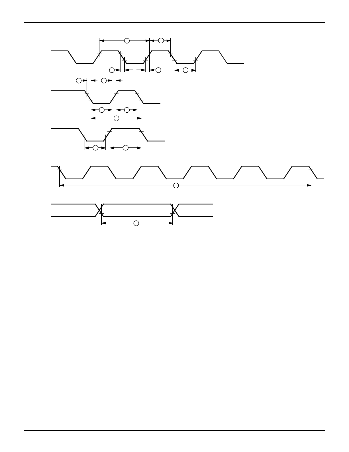
Handshake Timing Diagrams
Data In
/DAV
(Input)
RDY
(Output)
Data Out
Data In Valid
1
7
Next Data In Valid
2
3
Delayed DAV
4 5 6
Delayed RDY
Figure 16. Input Handshake Timing
Data Out Valid
Next Data Out Valid
/DAV
(Output)
RDY
(Input)
8 9
10
Figure 17. Output Handshake Timing
Delayed DAV
11
Delayed RDY
22 P R E L I M I N A R Y DS97Z8X0500

Z86E30/E31/E40
1
Zilog Z8 4K OTP Microcontroller
Additional Timing Table
TA = -40 °C to +105 °C
16 MHz
V
CC
No Symbol Parameter
1 TpC Input Clock Period 3.5V
2 TrC,TfC Clock Input Rise &
Fall Times
3 TwC Input Clock Width 3.5V
4 TwTinL Timer Input Low
Width
5 TwTinH Timer Input High
Width
6 TpTin Timer Input Period 3.5V
7 TrTin, TfTin Timer Input Rise
& Fall Timer
8A TwIL Int. Request Low
Time
8B TwIL Int. Request Low
Time
9 TwIH Int. Request Input
High Time
10 Twsm STOP Mode
Recovery Width
Spec
11 Tost Oscillator Startup
Time
12 T wdt Watch-Dog Timer
Delay Time
Before Timeout
Notes:
1. Timing Reference uses 0.7 VCC for a logic 1 and 0.2 VCC for a logic 0
2. Interrupt request via Port 3 (P31-P33)
3. Interrupt request via Port 3 (P30)
4. SMR-D5 = 1, POR STOP Mode Delay is on
5. Reg. WDTMR
6. The VCC voltage spec. of 5.5V guarantees 5.0V +/- ± 0.5V
7. SMR D1 = 0
8. Maximum frequency for internal system clock is 4 MHz when using
XTAL divide-by-one mode.
9. For RC and LC oscillator, and for oscillator driven by clock driver.
10. Standard Mode (not Low EMI output ports)
11. Using internal RC
Note [6] Min Max Units Conditions Notes
5.5V
3.5V
5.5V
5.5V
3.5V
5.5V
3.5V
5.5V
5.5V
3.5V
5.5V
3.5V
5.5V
3.5V
5.5V
3.5V
62.5
62.5
31
31
70
70
5TpC
5TpC
8TpC
8TpC
70
70
5TpC
5TpC
5TpC 1,2,7,8
DC
DC
15
15
100
100
ns
ns
ns
ns
ns
ns
ns
ns
ns
ns
ns
ns
1,7,8
1,7,8
1,7,8
1,7,8
1,7,8
1,7,8
1,7,8
1,7,8
1,7,8
1,7,8
[1,7,8
1,7,8
1,7,8
1,7,8
1,2,7,8
1,2,7,8
1,3,7,8
1,3,7,8
5.5V
3.5V
5.5V
3.5V
5.5V
3.5V
5.5V
3.5V
5.5V
3.5V
5.5V
3.5V
5.5V
12
12
10
5
20
10
40
20
160
80
5TpC
5TpC
ns
ns
ms
ms
ms
ms
ms
ms
ms
ms
D0 = 0
D1 = 0
D0 = 1
D1 = 0
D0 = 0
D1 = 1
D0 = 1
D1 = 1
4,8
4,8
4,8
4,8
5,11
5,11
5,11
5,11
5,11
5,11
5,11
5,11
DS97Z8X0500 P R E L I M I N A R Y 23

Z86E30/E31/E40
Z8 4K OTP Microcontroller Zilog
PIN FUNCTIONS
EPROM Programming Mode
D7-D0 Data Bus. The data can be read from or written to
external memory through the data bus.
A11-A0 Address Bus. During programming, the EPROM
address is written to the address bus.
VCC Power Supply. This pin must supply 5V during the
EPROM read mode and 6V during other modes.
/CE Chip Enable (active Low). This pin is active during
EPROM Read Mode, Program Mode, and Program Verify
Mode.
/OE Output Enable (active Low). This pin drives the direction of the Data Bus. When this pin is Low, the Data Bus is
output, when High, the Data Bus is input.
EPM EPROM Program Mode. This pin controls the different EPROM Program Mode by applying different voltages.
Program Voltage. This pin supplies the program volt-
V
PP
age.
/PGM Program Mode (active Low). When this pin is Low,
the data is programmed to the EPROM through the Data
Bus.
Application Precaution
The production test-mode environment may be enabled
accidentally during normal operation if excessive noise
surges above VCC occur on pins XTAL1 and /RESET.
In addition, processor operation of Z8 OTP devices may be
affected by excessive noise surges on the VPP, /CE, /EPM,
/OE pins while the microcontroller is in Standard Mode.
Recommendations for dampening voltage surges in both
test and OTP mode include the following:
R//W Read/Write (output, write Low). The R//W signal is
Low when the CCP is writing to the external program or
data memory (Z86E40 only).
/RESET Reset (input, active Low). Reset will initialize the
MCU. Reset is accomplished either through Power-On,
Watch-Dog Timer reset, STOP-Mode Recovery, or external reset. During Power-On Reset and Watch-Dog Timer
Reset, the internally generated reset drives the reset pin
low for the POR time. Any devices driving the reset line
must be open-drain in order to avoid damage from a possible conflict during reset conditions. Pull-up is provided internally. After the POR time, /RESET is a Schmitt-triggered input.
To avoid asynchronous and noisy reset problems, the
Z86E40 is equipped with a reset filter of four external
clocks (4TpC). If the external reset signal is less than 4TpC
in duration, no reset occurs. On the fifth clock after the reset is detected, an internal RST signal is latched and held
for an internal register count of 18 external clocks, or for
the duration of the external reset, whichever is longer. During the reset cycle, /DS is held active Low while /AS cycles
at a rate of TpC/2. Program execution begins at location
000CH, 5-10 TpC cycles after /RESET is released. For
Power-On Reset, the reset output time is 5 ms. The
Z86E40 does not reset WDTMR, SMR, P2M, and P3M
registers on a STOP-Mode Recovery operation.
/ROMless (input, active Low). This pin, when connected to
GND, disables the internal ROM and forces the device to
function as a Z86C90/C89 ROMless Z8. (Note that, when
left unconnected or pulled High to VCC, the device functions normally as a Z8 ROM version).
Note: When using in ROM Mode in High EMI (noisy) environment, the ROMless pins should be connected directly
to VCC.
■ Using a clamping diode to V
■ Adding a capacitor to the affected pin
CC
Standard Mode
XTAL Crystal 1 (time-based input). This pin connects a
parallel-resonant crystal, ceramic resonator, LC, RC network, or external single-phase clock to the on-chip oscillator input.
XTAL2 Crystal 2 (time-based output). This pin connects a
parallel-resonant crystal, ceramic resonator, LC, or RC
network to the on-chip oscillator output.
24 P R E L I M I N A R Y DS97Z8X0500

Z86E30/E31/E40
1
Zilog Z8 4K OTP Microcontroller
Port 0 (P07-P00). Port 0 is an 8-bit, bidirectional, CMOS-
compatible I/O port. These eight I/O lines can be configured under software control as a nibble I/O port, or as an
address port for interfacing external memory. The input
buffers are Schmitt-triggered and nibble programmed. Either nibble output that can be globally programmed as
push-pull or open-drain. Low EMI output buffers can be
globally programmed by the software. Port 0 can be placed
under handshake control. In Handshake Mode, Port 3
lines P32 and P35 are used as handshake control lines.
The handshake direction is determined by the configuration (input or output) assigned to Port 0's upper nibble. The
lower nibble must have the same direction as the upper
nibble.
For external memory references, Port 0 provides address
bits A11-A8 (lower nibble) or A15-A8 (lower and upper nibble) depending on the required address space. If the address range requires 12 bits or less, the upper nibble of
Port 0 can be programmed independently as I/O while the
lower nibble is used for addressing. If one or both nibbles
are needed for I/O operation, they must be configured by
writing to the Port 0 mode register. In ROMless mode, after
a hardware reset, Port 0 is configured as address lines
A15-A8, and extended timing is set to accommodate slow
memory access. The initialization routine can include reconfiguration to eliminate this extended timing mode. In
ROM mode, Port 0 is defined as input after reset.
Port 0 can be set in the High-Impedance Mode if selected
as an address output state, along with Port 1 and the control signals /AS, /DS, and R//W (Figure 18).
DS97Z8X0500 P R E L I M I N A R Y 25

Z86E30/E31/E40
Z8 4K OTP Microcontroller Zilog
4
Port 0 (I/O)
4
Handshake Controls
/DAV0 and RDY0
(P32 and P35)
Open-Drain
OEN
Out
In
PAD
1.5 2.3V Hysteresis
Auto Latch
R 500 kΩ
Figure 18. Port 0 Configuration
26 P R E L I M I N A R Y DS97Z8X0500

Z86E30/E31/E40
1
Zilog Z8 4K OTP Microcontroller
Port 1 (P17-P10). Port 1 is an 8-bit, bidirectional, CMOS-
compatible port with multiplexed Address (A7-A0) and
Data (D7-D0) ports. These eight I/O lines can be programmed as inputs or outputs or can be configured under
software control as an Address/Data port for interfacing
external memory. The input buffers are Schmitt-triggered
and the output buffers can be globally programmed as either push-pull or open-drain. Low EMI output buffers can
be globally programmed by the software. Port 1 can be
placed under handshake control. In this configuration, Port
3, lines P33 and P34 are used as the handshake controls
MCU
RDY1 and /DAV1 (Ready and Data Available). To interface external memory, Port 1 must be programmed for the
multiplexed Address/Data mode. If more than 256 external
locations are required, Port 0 outputs the additional lines
(Figure 19).
Port 1 can be placed in the high-impedance state along
with Port 0, /AS, /DS, and R//W, allowing the Z86E40 to
share common resources in multiprocessor and DMA applications.
Port 2 (I/O)
Handshake Controls
/DAV1 and RDY1
(P33 and P34)
Open-Drain
OEN
Out
In
PAD
1.5 2.3V Hysteresis
Auto Latch
R 500 kΩ
Figure 19. Port 1 Configuration (Z86E40 Only)
DS97Z8X0500 P R E L I M I N A R Y 27

Z86E30/E31/E40
Z8 4K OTP Microcontroller Zilog
Port 2 (P27-P20). Port 2 is an 8-bit, bidirectional, CMOS-
compatible I/O port. These eight I/O lines can be configured under software control as an input or output, independently. All input buffers are Schmitt-triggered. Bits programmed as outputs can be globally programmed as
either push-pull or open-drain. Low EMI output buffers can
Z86E40
MCU
be globally programmed by the software. When used as an
I/O port, Port 2 can be placed under handshake control.
In Handshake Mode, Port 3 lines P31 and P36 are used as
handshake control lines. The handshake direction is determined by the configuration (input or output) assigned to bit
7 of Port 2 (Figure 20).
Port 2 (I/O)
Handshake Controls
/DAV2 and RDY2
(P31 and P36)
Open-Drain
OEN
Out
In
PAD
TTL Level Shifter
Auto Latch
R ≈ 500 KΩ
Figure 20. Port 2 Configuration
28 P R E L I M I N A R Y DS97Z8X0500

Z86E30/E31/E40
1
Zilog Z8 4K OTP Microcontroller
Port 3 (P37-P30). Port 3 is an 8-bit, CMOS-compatible
port with four fixed inputs (P33-P30) and four fixed outputs
(P37-P34). These eight lines can be configured by software for interrupt and handshake control functions. Port 3,
Pin 0 is Schmitt- triggered. P31, P32 and P33 are standard
CMOS inputs with single trip point (no Auto Latches) and
P34, P35, P36 and P37 are push-pull output lines. Low
EMI output buffers can be globally programmed by the
software. Two on-board comparators can process analog
signals on P31 and P32 with reference to the voltage on
P33. The analog function is enabled by setting the D1 of
Port 3 Mode Register (P3M). The comparator output can
be outputted from P34 and P37, respectively, by setting
PCON register Bit D0 to 1 state. For the interrupt function,
P30 and P33 are falling edge triggered interrupt inputs.
P31 and P32 can be programmed as falling, rising or both
edges triggered interrupt inputs (Figure 21). Access to
Counter/Timer 1 is made through P31 (T
(T
). Handshake lines for Port 0, Port 1, and Port 2 are
OUT
also available on Port 3 (Table 9).
) and P36
IN
Note: P33-P30 differs from the Z86C30/C31/C40 in that
there is no clamping diode to V
voltage circuits. Exceeding the VIH maximum specification
during standard operating mode may cause the device to
enter EPROM mode.
due to the EPROM high-
CC
DS97Z8X0500 P R E L I M I N A R Y 29

Z86E30/E31/E40
Z8 4K OTP Microcontroller Zilog
P30
Z86E40
MCU
R247 = P3M
R ≈ 500 KΩ
D1
Port 3
(I/O or Control)
Auto Latch
P30 Data
Latch IRQ3
1 = Analog
0 = Digital
P31 (AN1)
P32 (AN2)
P33 (REF)
From Stop Mode
Recovery Source
DIG.
IRQ2, Tin, P31 Data Latch
+
AN.
-
IRQ0, P32 Data Latch
+
-
IRQ1, P33 Data Latch
Figure 21. Port 3 Configuration
30 P R E L I M I N A R Y DS97Z8X0500

Z86E30/E31/E40
1
Zilog Z8 4K OTP Microcontroller
Table 9. Port 3 Pin Assignments
Pin I/O CTC1 Analog Interrupt P0 HS P1 HS P2 HS Ext
P30 IN IRQ3
P31 IN T
P32 IN AN2 IRQ0 D/R
P33 IN REF IRQ1 D/R
P34 OUT AN1-Out R/D /DM
P35 OUT R/D
P36 OUT T
P37 OUT An2-Out
IN
OUT
AN1 IRQ2 D/R
R/D
Comparator Inputs. Port 3, P31, and P32, each have a
comparator front end. The comparator reference voltage
P33 is common to both comparators. In analog mode, P31
and P32 are the positive input of the comparators and P33
is the reference voltage of the comparators.
Auto Latch. The Auto Latch puts valid CMOS levels on all
CMOS inputs (except P33-P31) that are not externally
driven. Whether this level is 0 or 1, cannot be determined.
A valid CMOS level, rather than a floating node, reduces
excessive supply current flow in the input buffer. Auto
Latches are available on Port 0, Port 2, and P30. There
are no Auto Latches on P31, P32, and P33.
Low EMI Emission. The Z86E40 can be programmed to
operate in a low EMI Emission Mode in the PCON register.
The oscillator and all I/O ports can be programmed as low
EMI emission mode independently. Use of this feature results in:
■ The pre-drivers slew rate reduced to 10 ns typical.
■ Low EMI output drivers have resistance of 200 Ohms
(typical).
■ Low EMI Oscillator.
■ Internal SCLK/TCLK= XTAL operation limited to a
maximum of 4 MHz - 250 ns cycle time, when Low EMI
Oscillator is selected and system clock (SCLK = XTAL,
SMR Reg. Bit D1 =1).
■ Note for emulation only:
Do not set the emulator to emulate Port 1 in low EMI
mode. Port 1 must always be configured in Standard
Mode.
DS97Z8X0500 P R E L I M I N A R Y 31

Z86E30/E31/E40
Z8 4K OTP Microcontroller Zilog
FUNCTIONAL DESCRIPTION
The MCU incorporates the following special functions to
enhance the standard Z8 architecture to provide the user
with increased design flexibility.
RESET. The device is reset in one of three ways:
1. Power-On Reset
2. Watch-Dog Timer
3. STOP-Mode Recovery Source
Note: Having the Auto Power-on Reset circuitry built-in,
the MCU does not need to be connected to an external
power-on reset circuit. The reset time is 5 ms (typical). The
MCU does not re-initialize WDTMR, SMR, P2M, and P3M
registers to their reset values on a STOP-Mode Recovery
operation.
EPROM ROMless
65535
External
4096
4095
ROM and RAM
On-Chip One Time PROM
Note: The device VCC must rise up to the operating V
specification before the TPOR expires.
Program Memory. The MCU can address up to 4 KB of
Internal Program Memory (Figure 22). The first 12 bytes of
program memory are reserved for the interrupt vectors.
These locations contain six 16-bit vectors that correspond
to the six available interrupts. For EPROM mode, byte 12
(000CH) to address 4095 (0FFFH) consists of programmable EPROM. After reset, the program counter points at
the address 000CH, which is the starting address of the
user program.
In ROMless mode, the Z86E40 can address up to 64 KB
of External Program Memory. The ROM/ROMless option
is only available on the 44-pin devices.
CC
External
ROM and RAM
Location of
First Byte of
Instruction
Executed
After RESET
Interrupt
Vector
(Lower Byte)
Interrupt
Vector
(Upper Byte)
12
11
10
IRQ5
IRQ5
9
8
7
6
5
4
3
2
1
0
IRQ4
IRQ4
IRQ3
IRQ3
IRQ2
IRQ2
IRQ1
IRQ1
IRQ0
IRQ0
IRQ5
IRQ5
IRQ4
IRQ4
IRQ3
IRQ3
IRQ2
IRQ2
IRQ1
IRQ1
IRQ0
IRQ0
Figure 22. Program Memory Map
(ROMless Z86E40 Only)
32 P R E L I M I N A R Y DS97Z8X0500

Z86E30/E31/E40
1
Zilog Z8 4K OTP Microcontroller
EPROM Protect. When in ROM Protect Mode, and exe-
cuting out of External Program Memory, instructions LDC,
LDCI, LDE, and LDEI cannot read Internal Program Memory.
When in ROM Protect Mode and executing out of Internal
Program Memory, instructions LDC, LDCI, LDE, and LDEI
can read Internal Program Memory.
Data Memory (/DM). In EPROM Mode, the Z86E40 can
address up to 60 KB of external data memory beginning at
EPROM ROMless
65535
location 4096. In ROMless mode, the Z86E40 can address
up to 64 KB of data memory. External data memory may
be included with, or separated from, the external program
memory space. /DM, an optional I/O function that can be
programmed to appear on pin P34, is used to distinguish
between data and program memory space (Figure 23).
The state of the /DM signal is controlled by the type of instruction being executed. An LDC opcode references
PROGRAM (/DM inactive) memory, and an LDE instruction references data (/DM active Low) memory.
4096
4095
External
Data
Memory
Not Addressable
0
Figure 23. Data Memory Map
External
Data
Memory
DS97Z8X0500 P R E L I M I N A R Y 33

Z86E30/E31/E40
Z8 4K OTP Microcontroller Zilog
Expanded Register File (ERF). The register file has been
expanded to allow for additional system control registers,
mapping of additional peripheral devices and input/output
ports into the register address area. The Z8 register address space R0 through R15 is implemented as 16 groups
of 16 registers per group (Figure 26). These register
groups are known as the Expanded Register File (ERF).
The low nibble (D3-D0) of the Register Pointer (RP) select
the active ERF group, and the high nibble (D7-D4) of register RP select the working register group. Three system
configuration registers reside in the Expanded Register
File at bank FH: PCON, SMR, and WDTMR. The rest of
the Expanded Register is not physically implemented and
is reserved for future expansion.
R253 RP
D7 D6 D5 D4 D3 D2 D1 D0
Register File. The register file consists of three I/O port
registers, 236/125 general-purpose registers, 15 control
and status registers, and three system configuration registers in the expanded register group. The instructions can
access registers directly or indirectly through an 8-bit address field. This allows a short 4-bit register address using
the Register Pointer (Figure 24). In the 4-bit mode, the register file is divided into 16 working register groups, each
occupying 16 continuous locations. The Register Pointer
addresses the starting location of the active working-register group.
Note: Register Bank E0-EF can only be accessed through
working register and indirect addressing modes. (This
bank is available in Z86E30/E40 only.)
Expanded Register Group
Default setting after RESET = 00000000
Figure 24. Register Pointer Register
Working Register Group
34 P R E L I M I N A R Y DS97Z8X0500

Z86E30/E31/E40
1
Zilog Z8 4K OTP Microcontroller
r7 r6 r5 r4 R253
r3 r2 r1 r0
(Register Pointer)
The upper nibble of the register file address
provided by the register pointer specifies
the active working-register group.
FF
Register Group F
F0
EF
Note: Registers 80H
through EFH are
available in the Z86C30
80
7F
70
6F
only.
60
5F
50
4F
40
3F
30
2F
20
1F
Specified Working
Register Group
Register Group 1
10
0F
Register Group 0
00
I/O Ports
* Expanded Register Group (0) is selected
in this figure by handling bits D3 to D0 as
"0" in Register R253 (RP).
Figure 25. Register Pointer
The lower nibble
of the register
file address
provided by the
instruction points
to the specified
register.
R15 to R0
R15 to R4*
R3 to R0*
DS97Z8X0500 P R E L I M I N A R Y 35

Z86E30/E31/E40
Z8 4K OTP Microcontroller Zilog
®
STANDARD CONTROL REGISTERS
Z8
RESET CONDITION
D7 D6 D5 D4 D3 D2 D1 D0
0
0
0
0
0
0
0
0
0
0
0
0
0
0
0
0
0
0
0
0
0
U
U
U
U
U
U
U
U
U
U
U
U
U
0
0
0
0
0
0
0
0
U
U
U
U
U
U
U
0
1
1
0
0
1
0
0
0
0
0
0
0
0
1
1
1
1
1
1
1
U
U
U
U
U
U
U
U
U
U
U
U
U
U
0
U
U
U
U
U
U
U
U
U
U
U
U
U
0
0
0
0
0
0
0
0
0
0
U
U
0
U
1
0
1
0
U
0
U
0
Working Register
Group Pointer
%FF
%FO
REGISTER POINTER
7
6543210
Z8 Reg. File
Z86E30/E40 Only
Expanded Register
Group Pointer
REGISTER
% FF
% FE
% FD
% FC
% FB
% FA
% F9
†
% F8
% F7
*
% F6
*
% F5
% F4
% F3
% F2
% F1
% F0
SPL
SPH
RP
FLAGS
IMR
IRQ
IPR
P01M
P3M
P2M
PRE0
T0
PRE1
T1
TMR
Reserved
%7F
%0F
%00
Notes:
U = Unknown
†
For Z86E40 (ROMless) reset condition: "10110110"
Will not be reset with a STOP Mode Recovery
*
Will not be reset with a STOP Mode Recovery, except Bit D0.
**
Z86E30/E40 Only
Reserved
EXPANDED REG. GROUP (F)
REGISTER
% (F) 0F
*
% (F) 0E
% (F) 0D
*
% (F) 0C
**
% (F) 0B
% (F) 0A
% (F) 09
% (F) 08
% (F) 07
% (F) 06
% (F) 05
% (F) 04
% (F) 03
% (F) 02
% (F) 01
% (F) 00
WDTMR
Reserved
SMR2
Reserved
SMR
Reserved
Reserved
Reserved
Reserved
Reserved
Reserved
Reserved
Reserved
Reserved
Reserved
PCON
EXPANDED REG. GROUP (0)
REGISTER
% (0) 03 P3
*
% (0) 02 P2
*
% (0) 01 P1
% (0) 00
P0
RESET CONDITION
UUU0 11 0 1
UUUUUU00
0010 000 0
1111 111 0
RESET CONDITION
1111UUUU
UUUUUUUU
UUUUUUUU
UUUUUUUU
Figure 26. Expanded Register File Architecture
36 P R E L I M I N A R Y DS97Z8X0500

Z86E30/E31/E40
1
Zilog Z8 4K OTP Microcontroller
General-Purpose Registers (GPR). These registers are
undefined after the device is powered up. The registers
keep their last value after any reset, as long as the reset
occurs in the VCC voltage-specified operating range. The
register R254 is general-purpose on Z86E30/E31. R254
and R255 are set to 00H after any reset or STOP-Mode recovery.
RAM Protect. The upper portion of the RAM's address
spaces 80H to EFH (excluding the control registers) can
be protected from reading and writing. This option can be
selected during the EPROM Programming Mode. After this
option is selected, the user can activate this feature from
the internal EPROM. D6 of the IMR control register (R251)
is used to turn off/on the RAM protect by loading a 0 or 1,
respectively. A 1 in D6 indicates RAM Protect enabled.
RAM Protect is not available on the Z86E31.
Stack. The Z86E40 external data memory or the internal
register file can be used for the stack. The 16-bit Stack
Pointer (R254-R255) is used for the external stack, which
can reside anywhere in the data memory for ROMless
mode, but only from 4096 to 65535 in ROM mode. An 8-bit
Stack Pointer (R255) is used for the internal stack on the
Z86E30/E31/E40 that resides within the 236 general-purpose registers (R4-R239). SPH (R254) can be used as a
general-purpose register when using internal stack only.
R254 and R255 are set to 00H after any reset or STOPMode Recovery.
Counter/Timers. There are two 8-bit programmable
counter/timers (T0 and T1), each driven by its own 6-bit
programmable prescaler. The T1 prescaler is driven by internal or external clock sources; however, the T0 prescaler
is driven by the internal clock only (Figure 27).
The 6-bit prescalers can divide the input frequency of the
clock source by any integer number from 1 to 64. Each
prescaler drives its counter, which decrements the value
(1 to 256) that has been loaded into the counter. When the
counter reaches the end of count, a timer interrupt request,
IRQ4 (T0) or IRQ5 (T1), is generated.
DS97Z8X0500 P R E L I M I N A R Y 37

Z86E30/E31/E40
Z8 4K OTP Microcontroller Zilog
38 P R E L I M I N A R Y DS97Z8X0500

Z86E30/E31/E40
1
Zilog Z8 4K OTP Microcontroller
The counters can be programmed to start, stop, restart to
continue, or restart from the initial value. The counters can
also be programmed to stop upon reaching zero (single
pass mode) or to automatically reload the initial value and
continue counting (modulo-n continuous mode).
The counters, but not the prescalers, can be read at any
time without disturbing their value or count mode. The
clock source for T1 is user-definable and can be either the
OSC
D1 (SMR)
Write Write Read
÷ 2
Initial Value
D0 (SMR)
÷ 16
÷4
internal microprocessor clock divided by four, or an external signal input through Port 3. The Timer Mode register
configures the external timer input (P31) as an external
clock, a trigger input that can be retriggerable or non-retriggerable, or as a gate input for the internal clock. Port 3 line
P36 serves as a timer output (T
) through which T0, T1
OUT
or the internal clock can be output. The counter/timers can
be cascaded by connecting the T0 output to the input of
T1.
Internal Data Bus
PRE0
Register
6-Bit
Down
Counter
T0
Initial Value
Register
8-bit
Down
Counter
T0
Current Value
Register
IRQ4
Clock
Logic
TIN P31
Internal
Clock
External Clock
÷4
Internal Clock
Gated Clock
Triggered Clock
6-Bit
Down
Counter
PRE1
Initial Value
Register
Write Write Read
8-Bit
Down
Counter
T1
Initial Value
Register
Internal Data Bus
Figure 27. Counter/Timer Block Diagram
÷2
Current Value
Register
TOUT
P36
IRQ5
T1
DS97Z8X0500 P R E L I M I N A R Y 39

Z86E30/E31/E40
Z8 4K OTP Microcontroller Zilog
Interrupts. The MCU has six different interrupts from six
different sources. The interrupts are maskable and prioritized (Figure 28). The six sources are divided as follows:
four sources are claimed by Port 3 lines P33-P30) and two
in counter/timers. The Interrupt Mask Register globally or
individually enables or disables the six interrupt requests
(Table 10).
IRQ0 IRQ2
IRQ1, 3, 4, 5
Interrupt
Edge
Select
IRQ
IMR
IRQ (D6, D7)
6
Global
Interrupt
Enable
Interrupt
Request
IPR
Priority
Logic
Vector Select
Figure 28. Interrupt Block Diagram
Table 10. Interrupt Types, Sources, and Vectors
Name Source Vector Location Comments
IRQ0 /DAV0, IRQ0 0, 1 External (P32), Rising/Falling Edge Triggered
IRQ1 IRQ1 2, 3 External (P33), Falling Edge Triggered
IRQ2 /DAV2, IRQ2, T
IN
4, 5 External (P31), Rising/Falling Edge Triggered
IRQ3 IRQ3 6, 7 External (P30), Falling Edge Triggered
IRQ4 T0 8, 9 Internal
IRQ5 TI 10, 11 Internal
40 P R E L I M I N A R Y DS97Z8X0500

Z86E30/E31/E40
1
Zilog Z8 4K OTP Microcontroller
When more than one interrupt is pending, priorities are resolved by a programmable priority encoder that is controlled by the Interrupt Priority Register (IPR). An interrupt
machine cycle is activated when an interrupt request is
granted. Thus, disabling all subsequent interrupts, saves
the Program Counter and Status Flags, and then branches
to the program memory vector location reserved for that interrupt. All interrupts are vectored through locations in the
program memory. This memory location and the next byte
contain the 16-bit starting address of the interrupt service
routine for that particular interrupt request.
To accommodate polled interrupt systems, interrupt inputs
are masked and the interrupt request register is polled to
determine which of the interrupt requests need service.
An interrupt resulting from AN1 is mapped into IRQ2, and
an interrupt from AN2 is mapped into IRQ0. Interrupts
IRQ2 and IRQ0 may be rising, falling or both edge triggered, and are programmable by the user. The software
may poll to identify the state of the pin.
Programming bits for the Interrupt Edge Select are located
in bits D7 and D6 of the IRQ Register (R250). The configuration is shown in Table 11.
Table 11. IRQ Register Configuration
IRQ Interrupt Edge
D7 D6 P31 P32
00FF
01FR
10RF
1 1 R/F R/F
Notes:
F = Falling Edge
R = Rising Edge
Clock. The on-chip oscillator has a high-gain, parallel-resonant amplifier for connection to a crystal, RC, ceramic
resonator, or any suitable external clock source (XTAL1 =
Input, XTAL2 = Output). The crystal should be AT cut, 10
KHz to 16 MHz max, with a series resistance (RS) less
than or equal to 100 Ohms.
The crystal should be connected across XTAL1 and
XTAL2 using the vendor's recommended capacitor values
from each pin directly to device pin Ground. The RC oscillator option can be selected in the programming mode.
The RC oscillator configuration must be an external resistor connected from XTAL1 to XTAL2, with a frequency-setting capacitor from XTAL1 to Ground (Figure 29).
XTAL1
C1
C1
XTAL2
C2
Ceramic Resonator or
Crystal
C2
LC
C1, C2 = 22 pF
C1, C2 = 47 pF TYP *
F = 8 MHz
L = 130 µH *
F = 3 MHz *
* Typical value including pin parasitics
Figure 29. Oscillator Configuration
XTAL1
XTAL1
C1
LR
XTAL2
RC
XTAL2
External Clock
@ 5V Vcc (TYP)
C1 = 100 pF
R = 2K
F = 6 MHz
XTAL1
XTAL2
DS97Z8X0500 P R E L I M I N A R Y 41

Z86E30/E31/E40
Z8 4K OTP Microcontroller Zilog
Power-On Reset (POR). A timer circuit clocked by a ded-
icated on-board RC oscillator is used for the Power-On Reset (POR) timer function. The POR timer allows V
CC
and
the oscillator circuit to stabilize before instruction execution begins.
The POR timer circuit is a one-shot timer triggered by one
of three conditions:
1. Power fail to Power OK status
2. STOP-Mode Recovery (if D5 of SMR=0)
3. WDT time-out
The POR time is a nominal 5 ms. Bit 5 of the STOP mode
Register (SMR) determines whether the POR timer is bypassed after STOP-Mode Recovery (typical for an external
clock and RC/LC oscillators with fast start up times).
HALT. Turns off the internal CPU clock, but not the XTAL
oscillation. The counter/timers and external interrupt IRQ0,
IRQ1, and IRQ2 remain active. The device is recovered by
interrupts, either externally or internally generated. An interrupt request must be executed (enabled) to exit HALT
mode. After the interrupt service routine, the program continues from the instruction after the HALT.
In order to enter STOP or HALT mode, it is necessary to
first flush the instruction pipeline to avoid suspending execution in mid-instruction. To do this, the user must execute
a NOP (opcode=FFH) immediately before the appropriate
sleep instruction, that is:
FF NOP ; clear the pipeline
6F STOP ; enter STOP
;mode
or
FF NOP ; clear the pipeline
7F HALT ; enter HALT mode
STOP. This instruction turns off the internal clock and external crystal oscillation and reduces the standby current
to 10 microamperes or less. STOP mode is terminated by
one of the following resets: either by WDT time-out, POR,
a STOP-Mode Recovery Source, which is defined by the
SMR register or external reset. This causes the processor
to restart the application program at address 000CH.
Port Configuration Register (PCON). The PCON register configures the ports individually; comparator output on
Port 3, open-drain on Port 0 and Port 1, low EMI on Ports
0, 1, 2 and 3, and low EMI oscillator. The PCON register is
located in the expanded register file at Bank F, location 00
(Figure 30).
42 P R E L I M I N A R Y DS97Z8X0500

Z86E30/E31/E40
1
Zilog Z8 4K OTP Microcontroller
PCON (FH) 00H
D7 D6 D5 D4 D3 D2 D1 D0
* Default Setting After Reset
Comparator Output Port 3
0 P34, P37 Standard Output*
1 P34, P37 Comparator Output
0 Port 1 Open Drain
1 Port 1 Push-pull Active*
0 Port 0 Open Drain
1 Port 0 Push-pull Active*
0 Port 0 Low EMI
1 Port 0 Standard*
0 Port 1 Low EMI
1 Port 1 Standard*
0 Port 2 Low EMI
1 Port 2 Standard*
0 Port 3 Low EMI
1 Port 3 Standard*
Low EMI Oscillator
0 Low EMI
1 Standard*
Figure 30. Port Configuration Register (PCON)
(Write Only)
Comparator Output Port 3 (D0). Bit 0 controls the com-
parator output in Port 3. A "1" in this location brings the
comparator outputs to P34 and P37, and a "0" releases the
Port to its standard I/O configuration. The default value is
0.
Port 1 Open-Drain (D1). Port 1 can be configured as an
open-drain by resetting this bit (D1=0) or configured as
push-pull active by setting this bit (D1=1). The default value is 1.
Port 0 Open-Drain (D2). Port 0 can be configured as an
open-drain by resetting this bit (D2=0) or configured as
push-pull active by setting this bit (D2=1). The default value is 1.
Low EMI Port 0 (D3). Port 0 can be configured as a Low
EMI Port by resetting this bit (D3=0) or configured as a
Standard Port by setting this bit (D3=1). The default value
is 1.
Low EMI Port 1 (D4). Port 1 can be configured as a Low
EMI Port by resetting this bit (D4=0) or configured as a
Standard Port by setting this bit (D4=1). The default value
is 1. Note: The emulator does not support Port 1 low EMI
mode and must be set D4 = 1.
Low EMI Port 2 (D5). Port 2 can be configured as a Low
EMI Port by resetting this bit (D5=0) or configured as a
Standard Port by setting this bit (D5=1). The default value
is 1.
Low EMI Port 3 (D6). Port 3 can be configured as a Low
EMI Port by resetting this bit (D6=0) or configured as a
Standard Port by setting this bit (D6=1). The default value
is 1.
Low EMI OSC (D7). This bit of the PCON Register controls the low EMI noise oscillator. A "1" in this location configures the oscillator with standard drive. While a "0" configures the oscillator with low noise drive, however, it does
not affect the relationship of SCLK and XTAL. The low EMI
DS97Z8X0500 P R E L I M I N A R Y 43

Z86E30/E31/E40
Z8 4K OTP Microcontroller Zilog
mode will reduce the drive of the oscillator (OSC). The default value is 1. Note: 4 MHz is the maximum external
clock frequency when running in the low EMI oscillator
mode.
STOP-Mode Recovery Register (SMR). This register selects the clock divide value and determines the mode of
STOP-Mode Recovery (Figure 31). All bits are Write Only
SMR (F) 0B
D7 D6 D5 D4 D3 D2 D1 D0
except bit 7 which is a Read Only. Bit 7 is a flag bit that is
hardware set on the condition of STOP Recovery and reset by a power-on cycle. Bit 6 controls whether a low or
high level is required from the recovery source. Bit 5 controls the reset delay after recovery. Bits 2, 3, and 4 of the
SMR register specify the STOP-Mode Recovery Source.
The SMR is located in Bank F of the Expanded Register
Group at address 0BH.
SCLK/TCLK Divide by 16
0 OFF
**
1 ON
External Clock Divide by 2
0 SCLK/TCLK =XTAL/2*
1 SCLK/TCLK =XTAL
Stop Mode Recovery Source
000 POR and/or External Reset
*
001 P30
010 P31
011 P32
100 P33
101 P27
110 P2 NOR 0:3
111 P2 NOR 0:7
Stop Delay
0 OFF
1 ON
*
Stop Recovery Level
0 Low
*
1 High
Stop Flag
0 POR
*
1 Stop Recovery
* Default setting after RESET.
** Default setting after RESET and STOP-Mode Recovery.
Figure 31. STOP-Mode Recovery Register
(Write-Only Except Bit D7, Which is Read-Only)
44 P R E L I M I N A R Y DS97Z8X0500

Z86E30/E31/E40
1
Zilog Z8 4K OTP Microcontroller
SCLK/TCLK Divide-by-16 Select (D0). This bit of the
SMR controls a divide-by-16 prescaler of SCLK/TCLK.
The purpose of this control is to selectively reduce device
power consumption during normal processor execution
(SCLK control) and/or HALT mode (where TCLK sources
counter/timers and interrupt logic).
External Clock Divide-by-Two (D1). This bit can eliminate the oscillator divide-by-two circuitry. When this bit is
0, the System Clock (SCLK) and Timer Clock (TCLK) are
equal to the external clock frequency divided by two. The
SCLK/TCLK is equal to the external clock frequency when
this bit is set (D1=1). Using this bit together with D7 of
SMR2 D1 D0
0 0
VDD
PCON further helps lower EMI (i.e., D7 (PCON) = 0, D1
(SMR) = 1). The default setting is zero.
STOP-Mode Recovery Source (D2, D3, and D4). These
three bits of the SMR register specify the wake up source
of the STOP-Mode Recovery (Figure 32). Table 12 shows
the SMR source selected with the setting of D2 to D4. P33P31 cannot be used to wake up from STOP mode when
programmed as analog inputs. When the STOP-Mode Recovery sources are selected in this register then SMR2
register bits D0, D1 must be set to zero.
Note: If the Port2 pin is configured as an output, this output
level will be read by the SMR circuitry..
P20
P23
SMR2 SMR2D1 D0
0 1
P20
P27
D1 D0
1 0
SMR D4 D3 D2
0 0 0
VDD
Stop-Mode Recovery Edge
Select (SMR)
P33 From Pads
Digital/Analog Mode
Select (P3M)
SMR SMR SMRD4 D3 D2
P30
P31
P32
0 0 1
0 1 0
0 1 1
P33 P27
D4 D3 D2
1 0 0
D4 D3 D2
1 0 1
P20
P23
SMR SMRD4 D3 D2
1 1 0
Figure 32. STOP-Mode Recovery Source
D4 D3 D2
1 1 1
P20
P27
To POR
RESET
To P33 Data
Latch and IRQ1
MUX
DS97Z8X0500 P R E L I M I N A R Y 45

Z86E30/E31/E40
Z8 4K OTP Microcontroller Zilog
Table 12. STOP-Mode Recovery Source
D4 D3 D2 SMR Source selection
0 0 0 POR recovery only
0 0 1 P30 transition
0 1 0 P31 transition (Not in analog
mode)
0 1 1 P32 transition (Not in analog
mode)
1 0 0 P33 transition (Not in analog
mode)
1 0 1 P27 transition
1 1 0 Logical NOR of Port 2 bits 0-3
1 1 1 Logical NOR of Port 2 bits 0-7
STOP-Mode Recovery Delay Select (D5). The 5 ms RESET delay after STOP-Mode Recovery is disabled by programming this bit to a zero. A 1 in this bit will cause a 5 ms
RESET delay after STOP-Mode Recovery. The default
condition of this bit is 1. If the fast wake up mode is selected, the STOP-Mode Recovery source needs to be kept active for at least 5TpC.
STOP-Mode Recovery Level Select (D6). A 1 in this bit
defines that a high level on any one of the recovery sources wakes the MCU from STOP mode. A 0 defines low level
recovery. The default value is 0.
Cold or Warm Start (D7). This bit is set by the device
upon entering STOP mode. A "0" in this bit indicates that
the device has been reset by POR (cold). A "1" in this bit
indicates the device was awakened by a SMR source
(warm).
STOP-Mode Recovery Register 2 (SMR2). This register
contains additional Stop-Mode Recovery sources. When
the Stop-Mode Recovery sources are selected in this register then SMR Register. Bits D2, D3, and D4 must be 0.
SMR:10 Operation
D1 D0 Description of Action
0 0 POR and/or external reset recovery
0 1 Logical AND of P20 through P23
1 0 Logical AND of P20 through P27
Watch-Dog Timer Mode Register (WDTMR). The WDT
is a retriggerable one-shot timer that resets the Z8 if it
reaches its terminal count. The WDT is disabled after Power-On Reset and initially enabled by executing the WDT instruction and refreshed on subsequent executions of the
WDT instruction. The WDT is driven either by an on-board
RC oscillator or an external oscillator from XTAL1 pin. The
POR clock source is selected with bit 4 of the WDT register.
Note: Execution of the WDT instruction affects the Z (Zero), S (Sign), and V (Overflow) flags.
WDT Time-Out Period (D0 and D1). Bits 0 and 1 control
a tap circuit that determines the time-out periods that can
beobtained (Table 13). The default value of D0 and D1
are 1 and 0, respectively.
Table 13. Time-out Period of WDT
D1 D0
Time-out of
the Internal
RC OSC
Time-out of
the System
Clock
0 0 5 ms 128 SCLK
0 1 10 ms* 256 SCLK*
1 0 20 ms 512 SCLK
1 1 80 ms 2048 SCLK
Notes:
*The default setting is 10 ms.
WDT During HALT Mode (D2). This bit determines
whether or not the WDT is active during HALT mode. A "1"
indicates that the WDT is active during HALT. A "0" disables the WDT in HALT mode. The default value is 1.
WDT During STOP Mode (D3). This bit determines
whether or not the WDT is active during STOP mode. A 1
indicates active during STOP. A "0" disables the WDT during STOP mode. This is applicable only when the WDT
clock source is the internal RC oscillator.
Clock Source For WDT (D4). This bit determines which
oscillator source is used to clock the internal POR and
WDT counter chain. If the bit is a 1, the internal RC oscillator is bypassed and the POR and WDT clock source is
driven from the external pin, XTAL1, and the WDT is
stopped in STOP mode. The default configuration of this
bit is 0, which selects the RC oscillator.
Permanent WDT. When this feature is enabled, the WDT
is enabled after reset and will operate in Run and Halt
mode. The control bits in the WDTMR do not affect the
WDT operation. If the clock source of the WDT is the internal RC oscillator, then the WDT will run in STOP mode. If
the clock source of the WDT is the XTAL1 pin, then the
WDT will not run in STOP mode.
Note: WDT time-out in Stop-Mode will not reset
SMR,SMR2,PCON, WDTMR, P2M, P3M, Ports 2 & 3 Data
Registers.
WDTMR Register Accessibility. The WDTMR register is
accessible only during the first 60 internal system clock
cycles from the execution of the first instruction after Power-On Reset, Watch-Dog reset or a STOP-Mode Recovery
46 P R E L I M I N A R Y DS97Z8X0500

Z86E30/E31/E40
1
Zilog Z8 4K OTP Microcontroller
(Figures 33 and 34). After this point, the register cannot be
modified by any means, intentional or otherwise. The
WDTMR (F) 0F
D7 D6 D5 D4 D3 D2 D1 D0
WDTMR cannot be read and is located in Bank F of the Expanded Register Group at address location 0FH.
WDT TAP INT RC OSC System Clock
00 5 ms 128 SCLK
01 10 ms 256 SCLK
10 20 ms 512 SCLK
11 80 ms 2048 SCLK
WDT During HALT
0 OFF
1 ON
WDT During STOP
0 OFF
1 ON
*
*
*
* Default setting after RESET
Figure 33. Watch-Dog Timer Mode Register
XTAL1/INT RC Select for WDT
0 On-Board RC
1 XTAL
Reserved (Must be 0)
Write Only
*
DS97Z8X0500 P R E L I M I N A R Y 47

Z86E30/E31/E40
Z8 4K OTP Microcontroller Zilog
/Reset
WDT Select
(WDTMR)
CLK Source
Select
(WDTMR)
XTAL
VDD
VLV
/WDT
4 Clock
Filter
Internal
RC OSC.
2V Operating
Voltage Det.
+
-
/Clear
CLK
M
U
X
5ms POR 5ms
CK
18 Clock RESET
Generator
WDT TAP SELECT
15ms
WDT/POR Counter Chain
/CLR
RESET
Internal
/RESET
25ms 100ms
From Stop
Mode
Recovery
Source
Stop Delay
Select (SMR)
Figure 34. Resets and WDT
Auto Reset Voltage. An on-board Voltage Comparator
checks that V
is at the required level to ensure correct
CC
operation of the device. Reset is globally driven if VCC is
below VLV (Figure 35).
Note: VCC must be in the allowed operating range prior to
the minimum Power-On Reset time-out (T
POR
).
48 P R E L I M I N A R Y DS97Z8X0500

Z86E30/E31/E40
1
Zilog Z8 4K OTP Microcontroller
VCC
(Volts)
3.7
3.5
3.3
3.1
2.9
2.7
2.5
2.3
-60 -40 -20 0 20 40 60 80 100 120 140
Temperature
(°C)
Figure 35. Typical Z86E40 VLV V oltage vs T emperature
DS97Z8X0500 P R E L I M I N A R Y 49

Z86E30/E31/E40
Z8 4K OTP Microcontroller Zilog
EPROM MODE.
Table 14 shows the programming voltages of each programming mode. Table 15, Figures 38, 39, and 40 show
the programming timing of each programming mode. Figure 41 shows the circuit diagram of a Z86E40 programming adaptor, which adapts from 2764A to Z86E40. Figure 43 shows the flow-chart of an Intelligent Programming
Algorithm, which is compatible with 2764A EPROM
(Z86E40 is 4K EPROM, 2764A is 8K EPROM). Since the
EPROM size of Z86E30/E31/E40 differs from 2764A, the
programming address range has to be set from 0000H to
0FFFH for the Z86E30/E40 and 0000H to 07FFH for
Z86E31. Otherwise, the upper portion of EPROM data will
overwrite the lower portion of EPROM data. Figure 39
shows the adaptation from the 2764A to Z86E30/E31.
Note: EPROM Protect feature allows the LDC, LDCI, LDE,
and LDEI instructions from internal program memory. A
ROM look-up table can be used with this feature.
During programming, the V
input pin supplies the pro-
PP
gramming voltage and current to the EPROM. This pin is
also used to latch which EPROM mode is to be used (R/W
EPROM or R/W Option bits). The mode is set by placing
the correct mode number on the least significant bits of the
address and raising the EPM pin above V. After a setup
time, the VPP pin can then be raised or lowered. The
latched EPROM mode will remain until the EPM pin is reduced below V
.
H
Mode Name Mode # LSB Addr
EPROM R/W 0 0000
Option Bit R/W 3 0011
EPROM R/W mode allows the programming of the user
mode program ROM.
Option Bit R/W allows the programming of the Z8 option
bits. When the device is latched into Option Bit R/W mode,
the address must then be changed to 63 decimals
(000000111111 Binary). The Options are mapped into this
address as follows:
Bit Option
7 Unused
6 Unused
5 32 KHz XTAL Option
4 Permanent WDT
3 Auto Latch Disable
2 RC Oscillator Option
1 RAM Protect
0 ROM Protect
Table 14. EPROM Programming Table
Programming
Modes
EPROM READ1 X V
EPROM READ2 X V
PROGRAM V
PROGRAM
V
PP
PP
V
PP
EPM /CE /OE /PGM ADDR DATA
H
H
V
H
V
H
VERIFY
OPTION BIT PGM V
PP
OPTION BIT READ X V
Notes:
V
= 13.0 V ± 0.1 V
H
= As per specific Z8 DC specification.
V
IH
VIL= As per specific Z8 DC specification.
X=Not used, but must be set to V
NU = Not used, but must be set to either V
during programming = 40 mA maximum.
I
PP
during programming, verify, or read = 40 mA maximum.
I
CC
has a tolerance of ±0.25V.
*V
CC
† Zilog recommends an EPROM read at V
ensure proper device operations during the V
but V
= 5.0 V is acceptable.
CC
H
V
H
H
, VIH, or VIL level.
or VIL level.
IH
= 4.5 V and 5.5 V to
CC
CC
Table 14 gives the proper conditions for EPROM R/W operations, once the mode is latched.
V
IL
V
IL
V
IL
V
IL
V
IL
V
IL
after programming,
V
IL
V
IL
V
IH
V
IL
V
IH
V
IL
*
V
CC
V
IH
V
IH
V
IL
V
IH
V
IL
V
IH
ADDR Out 4.5V†
ADDR Out 5.5V†
ADDR In 6.4V
ADDR Out 6.0V
63 IN 6.4V
63 OUT 6.0V
50 P R E L I M I N A R Y DS97Z8X0500

Z86E30/E31/E40
1
Zilog Z8 4K OTP Microcontroller
Table 15. EPROM Programming Timing
Parameters Name Min Max Units
1 Address Setup Time 2 µsµ
2 Data Setup Time 2 µs
3V
4V
5 Chip Enable Setup Time 2 µs
6 Program Pulse Width 0.95 1.05 ms
7 Data Hold Time 2 µs
8 /OE Setup Time 2 µs
9 Data Access Time 200 ns
10 Data Output Float Time 100 ns
11 Overprogram Pulse
12 EPM Setup Time 2 µs
13 /PGM Setup Time 2 µs
14 Address to /OE Setup Time 2 µsµ
15 /OE Width 250 ns
16 Address to /OE Low 125 ns
Setup 2 µs
PP
Setup Time 2 µs
CC
2.85 ms
Width/Option Program
Pulse Width
DS97Z8X0500 P R E L I M I N A R Y 51

Z86E30/E31/E40
Z8 4K OTP Microcontroller Zilog
VIH
Address
Data
VPP
EPM
VCC
/CE
VIL
VIH
VIL
VH
VIL
VH
VIL
4.5V
VIH
VIL
Address Stable
16
Address Stable
Invalid Valid Invalid Valid
9
12
5.5V
/OE
/PGM
VIH
VIL
VIH
VIL
5
15
3
15
Figure 36. EPROM Read Mode Timing Diagram
15
52 P R E L I M I N A R Y DS97Z8X0500

Z86E30/E31/E40
1
Zilog Z8 4K OTP Microcontroller
Z86E40 TIMING DIAGRAMS
Address
Data
VPP
EPM
VCC
/CE
VIH
VIL
VIH
VIL
VH
VIH
VH
VIL
6V
4.5V
VIH
VIL
Address Stable
1
Data Stable Data Out Valid
2 109
3
4
7
/OE
/PGM
VIH
VIL
VIH
VIL
5
6 8
11
Program Cycle Verify Cycle
Figure 37. Timing Diagram of EPROM Program and Verify Modes
15
DS97Z8X0500 P R E L I M I N A R Y 53

Z86E30/E31/E40
Z8 4K OTP Microcontroller Zilog
A0
A1
A2
A3
A4
A5
A6
A7
GND
D0
D1
D2
D3
D4
D5
D6
D7
A0
A1
A2
A3
A4
A5
A6
A7
A8
A9
A10
A11
A12
/PGM
/CS
/OE
2764 Pins
U2
00
01
02
03
04
05
06
07
GND
VCC
VPP
D0
11
D1
12
D2
13
15
D3
16
D4
17
D5
18
D6
19
D7
14
GND
28
VCC
1
C1
VPP
2
0.01µF
1
GND
U1
35
P20
36
P21
37
P22
38
P23
39
P24
2
P25
3
P26
4
P27
26
P00
27
P01
30
P02
34
P03
5
P04
6
P05
7
P06
10
P07
1
R//W
20
/AS
40
/DS
21
/RESET
XTAL1
XTAL2
P10
P11
P12
P13
P14
P15
P16
P17
P30
P31
P32
P33
P34
P35
P36
P37
28
29
32
33
8
9
12
13
25 /PGM
16 /0E
17
18
19
22
24
23
31
11
15
14
EPM
VPP
A8
A9
A10
A11
GND
VCC
/CE
1 KOhm
1 KOhm
R2
12
R1
12
A0
A1
A2
A3
A4
A5
A6
A7
A8
A9
A10
A11
10
9
8
7
6
5
4
3
25
24
21
23
2
27
20
22
Z86E40
40-Pin DIP
Socket
12.5V 16 X1
GND
4X3
VCC
15
IX1
4
S2
X
5
S4
X
10
IX2
X
R4
C2
0.1µF
12
1 KOhm
2
1
U3
D1
D3
12.5V
1
3
EPM
GND
5.0V
D2
3
X
D4 6
X
GND
5.0 V
VCC
IH5043
Figure 38. Z86E40 Z8 OTP Programming Adapter
For use with Standard EPROM Programmers
1N5243
GND
1N5231
1
2
R3
12
10 KOhm
D1
P1
R5
12
1 KOhm
1
D2
2
12.5 Volt
12
54 P R E L I M I N A R Y DS97Z8X0500

Z86E30/E31/E40
1
Zilog Z8 4K OTP Microcontroller
A0
A1
A2
A3
A4
A5
A6
A7
D0
D1
D2
D3
D4
D5
D6
D7
A0
A1
A2
A3
A4
A5
A6
A7
A8
A9
A10
A11
A12
/PGM
/CS
/OE
2764 Pins
U2
00
01
02
03
04
05
06
07
GND
VCC
VPP
D0
11
D1
12
D2
13
15
D3
16
D4
17
D5
18
D6
19
D7
14
GND
28
VCC
1
C1
VPP
2
0.01µF
1
GND
U1
24
P20
25
P21
26
P22
27
P23
28
P24
1
P25
2
P26
3
P27
19
P00
20
P01
21
P02
23
P03
4
P04
5
P05
6
P06
7
P07
XTAL1
XTAL2
P30
P31
P32
P33
P34
P35
P36
P37
18
/PGM
/OE
11
EPM
12
13
VPP
14
15
17
16
10
A8
A9
A10
A11
/CE
9
1 KOhm
1 KOhm
R2
12
R1
12
A4
A5
A6
A7
A0
A1
A2
A3
A4
A5
A6
A7
10
9
8
7
6
5
4
3
25
24
21
23
2
27
20
22
12.5V 16 X1
4X3
GND
15
VCC
IX1
4
S2
X
5
S4
X
10
IX2
X
Z86E30/31
28-Pin DIP
Socket
U3
VCC
D1
D3
D2
D4 6
1
3
3
X
X
5.0 V
12.5V
0.1µF
GND
EPM
Note: The programming address must be set to
C2
2
1
R4
12
1 KOhm
0000H - 0FFFH (Lower 4K Byte Memory). For Z86E30
IH5043
0000H - 07FFH (Lower 2K Byte Memory). For Z86E31
Figure 39. Z86E30/E31 Programming Adaptor Circuitry
5.0V
GND
1N5243
GND
1N5231
R3
12
10 KOhm
1
D1
2
1 KOhm
1
D2
2
12
P1
R5
12
12.5 Volt
DS97Z8X0500 P R E L I M I N A R Y 55

Z86E30/E31/E40
Z8 4K OTP Microcontroller Zilog
Start
Addr =
First Location
Vcc = 6.0V
Vpp = 12.5V
N = 0
Program
1 ms Pulse
Increment N
Increment
Address
Note:
* To ensure proper operaton,
Zilog recommends Vcc range
of the device Vcc specification,
But Vcc = 5.0V is acceptable.
N = 25 ?
No
Fail
One Byte
Pass
Prog. One Pulse
3xN ms Duration
No
Last Addr ?
Yes
Vcc = Vpp = 4.5V *
Verify All
Bytes
Pass
Vcc = Vpp = 5.5V *
Verify
Yes
Fail
Verify Byte
Pass
Device Failed
Fail
Verify All
Bytes
Pass
Device Passed
Fail
Figure 40. Z86E40 Programming Algorithm
56 P R E L I M I N A R Y DS97Z8X0500

Z86E30/E31/E40
1
Zilog Z8 4K OTP Microcontroller
EXPANDED REGISTER FILE CONTROL REGISTERS
PCON (FH) 00H
D7 D6 D5 D4 D3 D2 D1 D0
* Default Setting After Reset
† Must Be 1 for Z86E30/E31
Figure 41. Port Configuration Register
Write Only
Comparator Output Port 3
0 P34, P37 Standard*
1 P34, P37 Comparator Output
0 Port 1 Open-Drain
1 Port 1 Push-Pull Active*†
0 Port 0 Open-Drain
1 Port 0 Push-pull Active*
0 Port 0 Low EMI
1 Port 0 Standard*
0 Port 1 Low EMI
1 Port 1 Standard*†
0 Port 2 Low EMI
1 Port 2 Standard*
0 Port 3 Low EMI
1 Port 3 Standard*
Low EMI Oscillator
0 Low EMI
1 Standard*
WDTMR (F) 0F
D7 D6 D5 D4 D3 D2 D1 D0
WDT TAP INT RC OSC System Clock
00 5 ms 128 SCLK
01 10 ms 256 SCLK
*
10 20 ms 512 SCLK
11 80 ms 2048 SCLK
WDT During HALT
0 OFF
*
1 ON
WDT During STOP
0 OFF
1 ON
*
XTAL1/INT RC Select for WDT
0 On-Board RC
1 XTAL
Reserved (Must be 0)
* Default setting after RESET
Figure 43. Watch-Dog Timer Mode Register
Write Only
SMR2 (0F) DH
D7 D6 D5 D4 D3 D2 D1 D0
*
SMR (FH) 0B
D7 D6 D5 D4 D3 D2 D1 D0
SCLK/TCLK Divide-by-16
0 OFF
**
1 ON
External Clock Divide by 2
0 SCLK/TCLK =XTAL/2*
1 SCLK/TCLK =XTAL
Stop Mode Recovery Source
000 POR Only and/or External Reset*
001 P30
010 P31
011 P32
100 P33
101 P27
110 P2 NOR 0-3
111 P2 NOR 0-7
Stop Delay
0 OFF
1 ON*
Stop Recovery Level
0 Low*
1 High
Stop Flag
0 POR*
* Default setting after RESET.
** Default setting after RESET and STOP-Mode Recovery.
1 Stop Recovery
Figure 42. STOP-Mode Recovery Register
Write Only Except Bit D7, Which is Read Only
Stop-Mode Recovery Source 2
00 POR only*
01 AND P20,P21,P22,P23
10 AND P20,P21,P22,P23,P24,
P25,P26,P27
Reserved (Must be 0)
Note: Not used in conjunction with SMR Source
Figure 44. STOP-Mode Recovery Register 2
Write Only
DS97Z8X0500 P R E L I M I N A R Y 57

Z86E30/E31/E40
Z8 4K OTP Microcontroller Zilog
Z8 CONTROL REGISTER DIAGRAMS
R240
D7 D6 D5 D4 D3 D2 D1 D0
Figure 45. Reserved
R241 TMR
D7 D6 D5 D4 D3 D2 D1 D0
Reserved (Must be 0)
0 No Function*
1 Load T0
0 Disable T0 Count*
1 Enable T0 Count
0 No Function*
1 Load T1
0 Disable T1 Count*
1 Enable T1 Count
TIN Modes
00 External Clock Input*
01 Gate Input
10 Trigger Input
(Non-retriggerable)
11 Trigger Input
(Retriggerable)
R243 PRE1
D7 D6 D5 D4 D3 D2 D1 D0
*Default After Reset
Figure 48. Prescaler 1 Register
F3H: Write Only
R244 T0
D7 D6 D5 D4 D3 D2 D1 D0
Count Mode
0 T1 Single Pass*
1 T1 Modulo N
Clock Source
1 T1 Internal
0 T1 External Timing Input
(TIN Mode)
Prescaler Modulo
(Range: 1-64 Decimal
01-00 HEX)
T0 Initial Value
(When Written)
(Range: 1-256 Decimal
01-00 HEX)
T0 Current Value
(When Read)
Default After Reset = 00H
Figure 46. Timer Mode Register
F1H: Read/Write
R242 T1
D7 D6 D5 D4 D3 D2 D1 D0
Figure 47. Counter/Timer 1 Register
F2H: Read/Write
TOUT Modes
00 Not Used*
01 T0 Out
10 T1 Out
11 Internal Clock Out
T1 Initial Value
(When Written)
(Range: 1-256 Decimal
01-00 HEX)
T1 Current Value
(When Read)
Figure 49. Counter/Timer 0 Register
F4H; Read/Write
R245 PRE0
D7 D6 D5 D4 D3 D2 D1 D0
Count Mode
0 T1 Single Pass
1 T1 Modulo N
Reserved (Must be 0)
Prescaler Modulo
(Range: 1-64 Decimal
01-00 HEX)
Figure 50. Prescaler 0 Register
F5H: Write Only
58 P R E L I M I N A R Y DS97Z8X0500

Z86E30/E31/E40
1
Zilog Z8 4K OTP Microcontroller
R246 P2M
D7 D6 D5 D4 D3 D2 D1 D0
* Default After Reset
Figure 51. Port 2 Mode Register
F6H: Write Only
R247 P3M
D7 D6 D5 D4 D3 D2 D1 D0
Default After Reset = 00H
† Z86E30/E31 Must Be 00
Figure 52. Port 3 Mode Register
F7H: Write Only
P20 - P27 I/O Definition
0 Defines Bit as Output
1 Defines Bit as Input*
0 Port 2 Open-Drain
1 Port 2 Push-pull Active
0 P31, P32 Digital Mode
1 P31, P32 Analog Mode
0 P32 = Input
P35 = Output
1 P32 = /DAV0/RDY0
P35 = RDY0//DAV0
00 P33 = Input
P34 = Output
01 P33 = Input
10 P34 = /DM
11 P33 = /DAV1/RDY1
P34 = RDY1//DAV1
0 P31 = Input (TIN)
P36 = Output (TOUT)
1 P31 = /DAV2/RDY2
P36 = RDY2//DAV2
0 P30 = Input
P37 = Output
Reserved (Must be 0)
R248 P01M
D7 D6 D5 D4 D3 D2 D1 D0
Reset Condition = 0100 1101B
For ROMless Condition = 1011 0110B
† Z86E30/E31 Must be 00
Figure 53. Port 0 and 1 Mode Register
†
R249 IPR
D7 D6 D5 D4 D3 D2 D1 D0
P03 - P00 Mode
00 Output
01 Input
1X A11 - A8
Stack Selection
0 External
1 Internal
P17 - P10 Mode
00 Byte Output†
01 Byte Input
10 AD7 - AD0
11 High-Impedance AD7 - AD0,
/AS, /DS, /R//W, A11 - A8,
A15 - A12, If Selected
External Memory Timing
0 Normal
1 Extended
P07 - P04 Mode
00 Output
01 Input
1X A15 - A12
F8H: Write Only
Z86E30/E31 Only
Interrupt Group Priority
000 Reserved
001 C > A > B
010 A > B > C
011 A > C > B
100 B > C > A
101 C > B > A
110 B > A > C
111 Reserved
IRQ1, IRQ4 Priority (Group C)
0 IRQ1 > IRQ4
1 IRQ4 > IRQ1
IRQ0, IRQ2 Priority (Group B)
0 IRQ2 > IRQ0
1 IRQ0 > IRQ2
IRQ3, IRQ5 Priority (Group A)
0 IRQ5 > IRQ3
1 IRQ3 > IRQ5
Reserved (Must be 0)
Figure 54. Interrupt Priority Register
F9H: Write Only
DS97Z8X0500 P R E L I M I N A R Y 59

Z86E30/E31/E40
Z8 4K OTP Microcontroller Zilog
R250 IRQ
D7 D6 D5 D4 D3 D2 D1 D0
Default After Reset = 00H
Figure 55. Interrupt Request Register
FAH: Read/Write
R251 IMR
D7 D6 D5 D4 D3 D2 D1 D0
† This option must be selected when ROM code is
submitted for ROM Masking, otherwise this control bit
is disabled permanently.
IRQ0 = P32 Input
IRQ1 = P33 Input
IRQ2 = P31 Input
IRQ3 = P30 Input
IRQ4 = T0
IRQ5 = T1
Inter Edge
P31 ↓ P32 ↓ = 00
P31 ↓ P32 ↑ = 01
P31 ↑ P32 ↓ = 10
P31 ↑↓ P32 ↑↓ = 11
1 Enables IRQ5-IRQ0
(D0 = IRQ0)
1 Enables RAM Protect †
1 Enables Interrupts
R253 RP
D7 D6 D5 D4 D3 D2 D1 D0
Default After Reset = 00H
Figure 58. Register Pointer
FDH: Read/Write
R254 SPH
D7 D6 D5 D4 D3 D2 D1 D0
Figure 59. Stack Pointer High
FEH: Read/Write
R255 SPL
Expanded Register File
Working Register Pointer
(Z86E40)
Stack Pointer Upper
Byte (SP8 - SP15)
(Z86E30/E31)
0 = 0 State
1 = 1 State
Figure 56. Interrupt Mask Register
FBH: Read/Write
R252 FLAGS
D7 D6 D5 D4 D3 D2 D1 D0
Figure 57. Flag Register
FCH: Read/Write
D7 D6 D5 D4 D3 D2 D1 D0
Stack Pointer Lower
Byte (SP0 - SP7)
Figure 60. Stack Pointer Low
FFH: Read/Write
User Flag F1
User Flag F2
Half Carry Flag
Decimal Adjust Flag
Overflow Flag
Sign Flag
Zero Flag
Carry Flag
60 P R E L I M I N A R Y DS97Z8X0500
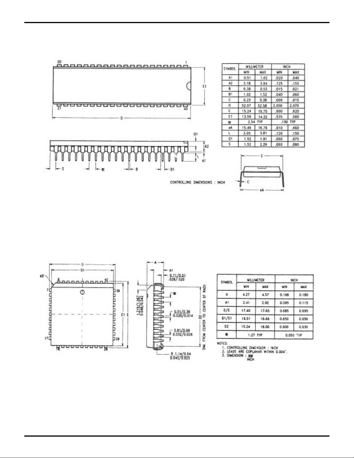
Z86E30/E31/E40
1
Zilog Z8 4K OTP Microcontroller
PACKAGE INFORMATION
Figure 61. 40-Pin DIP Package Diagram
Figure 62. 44-Pin PLCC Package Diagram
DS97Z8X0500 P R E L I M I N A R Y 61

Z86E30/E31/E40
Z8 4K OTP Microcontroller Zilog
Figure 63. 44-Pin QFP Package Diagram
Figure 64. 40-Pin Cerdip Window Lid Package Diagram
62 P R E L I M I N A R Y DS97Z8X0500

Z86E30/E31/E40
1
Zilog Z8 4K OTP Microcontroller
Figure 65. 28-Pin DIP Package Diagram
Figure 66. 28-Pin Window Cerdip Package Diagram
DS97Z8X0500 P R E L I M I N A R Y 63
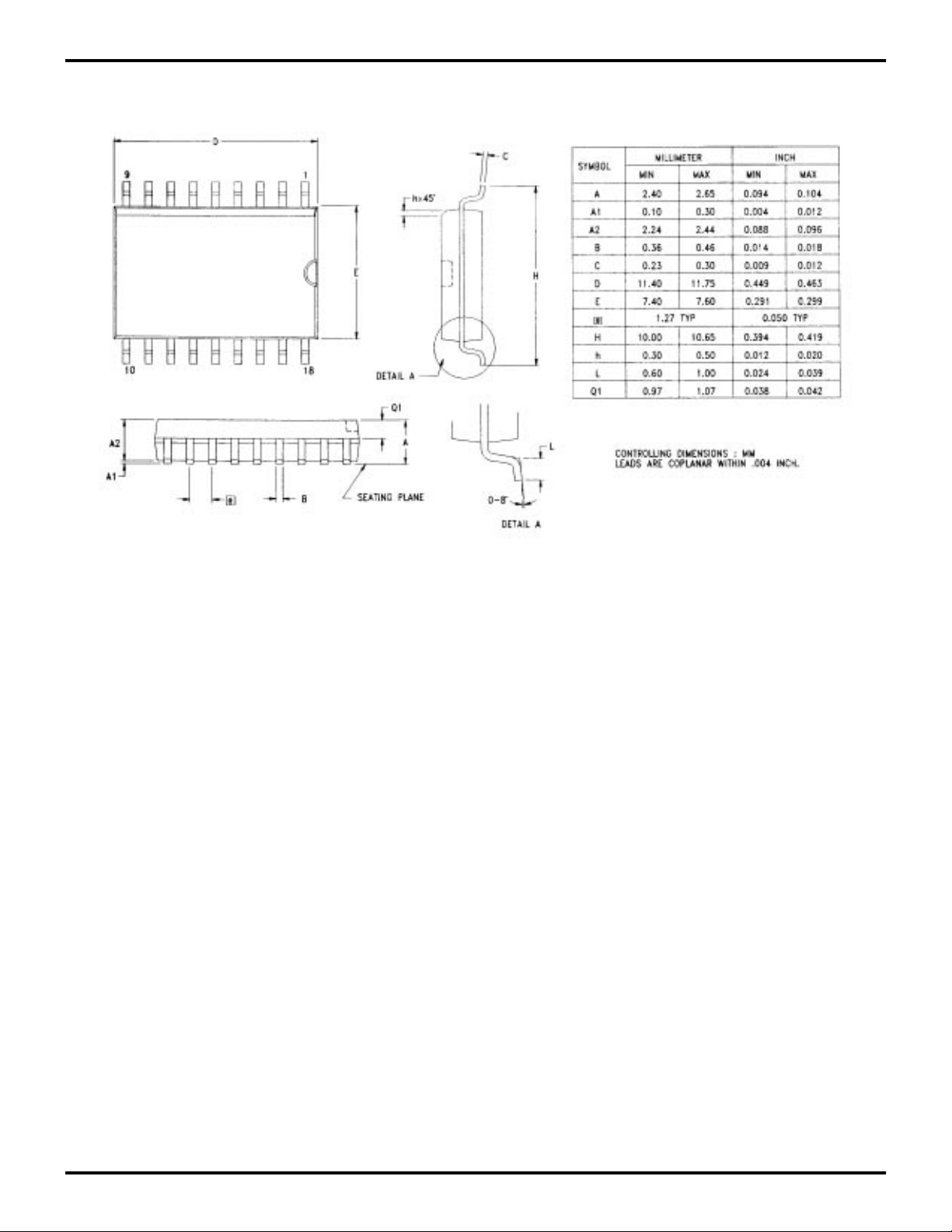
Z86E30/E31/E40
Z8 4K OTP Microcontroller Zilog
Figure 67. 18-Pin SOIC Package Diagram
64 P R E L I M I N A R Y DS97Z8X0500

Z86E30/E31/E40
1
Zilog Z8 4K OTP Microcontroller
ORDERING INFORMATION
Z86E40 (16 MHz)
40-Pin Cerdip
40-Pin DIP 44-Pin PLCC 44-Pin QFP
Z86E4016PSC Z86E4016VSC Z86E4016FSC Z86E4016ESE
Z86E4016PEC Z86E4016VEC Z86E4016FEC Z86E4016ESE
Z86E30 (16 MHz)
28-Pin Cerdip
28-Pin DIP
Z86E3016PSC Z86E3016ESE
Z96E3016PEC Z86E3016SSC
Z86E31 (16 MHz)
28-Pin DIP 28-Pin Cerdip
Z86E3116PSC Z86E3116SSC
For fast results, contact your local Zilog sales office for assistance in ordering the part desired.
Window Lid
Z86E3016SEC
Window Lid
Package
P = Plastic DIP
V = Plastic Chip Carrier
Window Lid
Temperature
S = 0 °C to +70 °C
E = -40 °C to +105 °C
Speed
F = Plastic Quad Flat Pack
K = Cerdip Window Lid
16 = 16 MHz
Environmental
C= Plastic Standard
E = Hermetic Standard
Example:
Z 86E40 16 P S C
DS97Z8X0500 P R E L I M I N A R Y 65
is a Z86E40, 16 MHz, DIP, 0°C to +70°C, Plastic Standard Flow
Environmental Flow
Temperature
Package
Speed
Product Number
Zilog Prefix

Z86E30/E31/E40
Z8 4K OTP Microcontroller Zilog
© 1997 by Zilog, Inc. All rights reserved. No part of this
document may be copied or reproduced in any form or by
any means without the prior written consent of Zilog, Inc.
The information in this document is subject to change
without notice. Devices sold by Zilog, Inc. are covered by
warranty and patent indemnification provisions appearing
in Zilog, Inc. Terms and Conditions of Sale only. Zilog, Inc.
makes no warranty, express, statutory, implied or by
description, regarding the information set forth herein or
regarding the freedom of the described devices from
intellectual property infringement. Zilog, Inc. makes no
warranty of merchantability or fitness for any purpose.
Zilog, Inc. shall not be responsible for any errors that may
appear in this document. Zilog, Inc. makes no commitment
to update or keep current the information contained in this
document.
66 P R E L I M I N A R Y DS97Z8X0500
Zilog’s products are not authorized for use as critical
components in life support devices or systems unless a
specific written agreement pertaining to such intended use
is executed between the customer and Zilog prior to use.
Life support devices or systems are those which are
intended for surgical implantation into the body, or which
sustains life whose failure to perform, when properly used
in accordance with instructions for use provided in the
labeling, can be reasonably expected to result in
significant injury to the user.
Zilog, Inc. 210 East Hacienda Ave.
Campbell, CA 95008-6600
Telephone (408) 370-8000
FAX 408 370-8056
Internet: http://www.zilog.com
 Loading...