

Page 1

Z8 Family of Microcontrollers
Z8® CPU
User Manual
UM001604-0108
Copyright ©2008 by Zilog®, Inc. All rights reserved.
www.zilog.com
Page 2

Z8® CPU
User Manual
ii
Warning:
LIFE SUPPORT POLICY
DO NOT USE IN LIFE SUPPORT
ZILOG'S PRODUCTS ARE NOT AUTHORIZED FOR USE AS CRITICAL COMPONENTS IN LIFE
SUPPORT DEVICES OR SYSTEMS WITHOUT THE EXPRESS PRIOR WRITTEN APPROVAL OF
THE PRESIDENT AND GENERAL COUNSEL OF ZILOG CORPORATION.
As used herein
Life support devices or systems are devices which (a) are intended for surgical implant into the body, or (b)
support or sustain life and whose failure to perform when properly used in accordance with instructions for
use provided in the labeling can be reasonably expected to result in a significant injury to the user. A
critical component is any component in a life support device or system whose failure to perform can be
reasonably expected to cause the failure of the life support device or system or to affect its safety or
effectiveness.
Document Disclaimer
©2008 by Zilog, Inc. All rights reserved. Information in this publication concerning the devices,
applications, or technology described is intended to suggest possible uses and may be superseded. ZILOG,
INC. DOES NOT ASSUME LIABILITY FOR OR PROVIDE A REPRESENTATION OF ACCURACY
OF THE INFORMATION, DEVICES, OR TECHNOLOGY DESCRIBED IN THIS DOCUMENT.
ZILOG ALSO DOES NOT ASSUME LIABILITY FOR INTELLECTUAL PROPERTY
INFRINGEMENT RELATED IN ANY MANNER TO USE OF INFORMATION, DEVICES, OR
TECHNOLOGY DESCRIBED HEREIN OR OTHERWISE. The information contained within this
document has been verified according to the general principles of electrical and mechanical engineering.
Z8 is the registered trademark of Zilog, Inc. All other product or service names are the property of their
respective owners.
UM001604-0108
Page 3

Revision History
Each instance in Revision History reflects a change to this document from its previous
revision. For more details, refer to the corresponding pages and appropriate links in the
table below.
Z8® CPU
User Manual
iii
Date Revision
Level
January
2008
February
2007
September
2004
04 Updated Zilog logo, Zilog text, Disclaimer section,
03 Changed the OP code to B0 and B1 in Instruction
02 Formatted to current publication standards. All pages
Description Page No
All
and implemented Style Guide.
167
Description.
UM001604-0108 Revision History
Page 4

Table of Contents
Z8® CPU Product Overview. . . . . . . . . . . . . . . . . . . . . . . . . . . . . . . . . . . . . . . . . . . . 1
Key Features . . . . . . . . . . . . . . . . . . . . . . . . . . . . . . . . . . . . . . . . . . . . . . . . . . . 1
Product Development Support . . . . . . . . . . . . . . . . . . . . . . . . . . . . . . . . . . . . . 3
Address Space . . . . . . . . . . . . . . . . . . . . . . . . . . . . . . . . . . . . . . . . . . . . . . . . . . . . . . 5
Introduction . . . . . . . . . . . . . . . . . . . . . . . . . . . . . . . . . . . . . . . . . . . . . . . . . . . . . . . 5
®
Z8
CPU Standard Register File . . . . . . . . . . . . . . . . . . . . . . . . . . . . . . . . . . . . . . . 5
General-Purpose Registers . . . . . . . . . . . . . . . . . . . . . . . . . . . . . . . . . . . . . . . . 7
RAM Protect . . . . . . . . . . . . . . . . . . . . . . . . . . . . . . . . . . . . . . . . . . . . . . . . . . . 7
Working Register Groups . . . . . . . . . . . . . . . . . . . . . . . . . . . . . . . . . . . . . . . . . 7
Error Conditions . . . . . . . . . . . . . . . . . . . . . . . . . . . . . . . . . . . . . . . . . . . . . . . 10
Z8 Expanded Register File . . . . . . . . . . . . . . . . . . . . . . . . . . . . . . . . . . . . . . . . . . 10
®
Z8
Control and Peripheral Registers . . . . . . . . . . . . . . . . . . . . . . . . . . . . . . . . . . 15
Standard Z8 Registers . . . . . . . . . . . . . . . . . . . . . . . . . . . . . . . . . . . . . . . . . . 15
Expanded Z8 Registers . . . . . . . . . . . . . . . . . . . . . . . . . . . . . . . . . . . . . . . . . . 16
Program Memory . . . . . . . . . . . . . . . . . . . . . . . . . . . . . . . . . . . . . . . . . . . . . . . . . . 19
®
Z8
External Memory . . . . . . . . . . . . . . . . . . . . . . . . . . . . . . . . . . . . . . . . . . . . . . 20
External Data Memory . . . . . . . . . . . . . . . . . . . . . . . . . . . . . . . . . . . . . . . . . . . 21
®
Z8
Stacks . . . . . . . . . . . . . . . . . . . . . . . . . . . . . . . . . . . . . . . . . . . . . . . . . . . . . . 22
Z8® CPU
User Manual
iv
Clock . . . . . . . . . . . . . . . . . . . . . . . . . . . . . . . . . . . . . . . . . . . . . . . . . . . . . . . . . . . . . 24
Frequency Control . . . . . . . . . . . . . . . . . . . . . . . . . . . . . . . . . . . . . . . . . . . . . . 24
Clock Control . . . . . . . . . . . . . . . . . . . . . . . . . . . . . . . . . . . . . . . . . . . . . . . . . . . . . 24
SCLK ÷ TCLK Divide-By-16 Select . . . . . . . . . . . . . . . . . . . . . . . . . . . . . . . . . 25
External Clock Divide-By-Two . . . . . . . . . . . . . . . . . . . . . . . . . . . . . . . . . . . . . 25
Oscillator Control . . . . . . . . . . . . . . . . . . . . . . . . . . . . . . . . . . . . . . . . . . . . . . . . . . 26
Oscillator Operation . . . . . . . . . . . . . . . . . . . . . . . . . . . . . . . . . . . . . . . . . . . . . . . 27
Layout . . . . . . . . . . . . . . . . . . . . . . . . . . . . . . . . . . . . . . . . . . . . . . . . . . . . . . . 28
Indications of an Unreliable Design . . . . . . . . . . . . . . . . . . . . . . . . . . . . . . . . . 28
Circuit Board Design Rules . . . . . . . . . . . . . . . . . . . . . . . . . . . . . . . . . . . . . . . 28
Crystals and Resonators . . . . . . . . . . . . . . . . . . . . . . . . . . . . . . . . . . . . . . . . . 29
LC Oscillator . . . . . . . . . . . . . . . . . . . . . . . . . . . . . . . . . . . . . . . . . . . . . . . . . . . . . 31
RC Oscillator . . . . . . . . . . . . . . . . . . . . . . . . . . . . . . . . . . . . . . . . . . . . . . . . . . . . . 32
Reset . . . . . . . . . . . . . . . . . . . . . . . . . . . . . . . . . . . . . . . . . . . . . . . . . . . . . . . . . . . . . 33
Reset Pin, Internal POR Operation . . . . . . . . . . . . . . . . . . . . . . . . . . . . . . . . . . . . 33
Watchdog Timer . . . . . . . . . . . . . . . . . . . . . . . . . . . . . . . . . . . . . . . . . . . . . . . . . . . . 40
Power-On Reset . . . . . . . . . . . . . . . . . . . . . . . . . . . . . . . . . . . . . . . . . . . . . . . . . . 42
UM001604-0108 Table of Contents
Page 5

Z8® CPU
User Manual
Input/Output Ports . . . . . . . . . . . . . . . . . . . . . . . . . . . . . . . . . . . . . . . . . . . . . . . . . . 43
Mode Registers . . . . . . . . . . . . . . . . . . . . . . . . . . . . . . . . . . . . . . . . . . . . . . . . 43
Input and Output Registers . . . . . . . . . . . . . . . . . . . . . . . . . . . . . . . . . . . . . . . 44
Port 0 . . . . . . . . . . . . . . . . . . . . . . . . . . . . . . . . . . . . . . . . . . . . . . . . . . . . . . . . . . . 44
General I/O Mode . . . . . . . . . . . . . . . . . . . . . . . . . . . . . . . . . . . . . . . . . . . . . . 45
Read/Write Operations . . . . . . . . . . . . . . . . . . . . . . . . . . . . . . . . . . . . . . . . . . 47
Handshake Operation . . . . . . . . . . . . . . . . . . . . . . . . . . . . . . . . . . . . . . . . . . . 47
Port 1 . . . . . . . . . . . . . . . . . . . . . . . . . . . . . . . . . . . . . . . . . . . . . . . . . . . . . . . . . . . 48
General I/O Mode . . . . . . . . . . . . . . . . . . . . . . . . . . . . . . . . . . . . . . . . . . . . . . 48
Read/Write Operations . . . . . . . . . . . . . . . . . . . . . . . . . . . . . . . . . . . . . . . . . . 50
Handshake Operations . . . . . . . . . . . . . . . . . . . . . . . . . . . . . . . . . . . . . . . . . . 51
Port 2 . . . . . . . . . . . . . . . . . . . . . . . . . . . . . . . . . . . . . . . . . . . . . . . . . . . . . . . . . . . 52
General Port I/O . . . . . . . . . . . . . . . . . . . . . . . . . . . . . . . . . . . . . . . . . . . . . . . 52
Read/Write Operations . . . . . . . . . . . . . . . . . . . . . . . . . . . . . . . . . . . . . . . . . . 54
Handshake Operation . . . . . . . . . . . . . . . . . . . . . . . . . . . . . . . . . . . . . . . . . . . 55
Port 3 . . . . . . . . . . . . . . . . . . . . . . . . . . . . . . . . . . . . . . . . . . . . . . . . . . . . . . . . . . . 56
General Port I/O . . . . . . . . . . . . . . . . . . . . . . . . . . . . . . . . . . . . . . . . . . . . . . . 56
Read/Write Operations . . . . . . . . . . . . . . . . . . . . . . . . . . . . . . . . . . . . . . . . . . 61
Special Functions . . . . . . . . . . . . . . . . . . . . . . . . . . . . . . . . . . . . . . . . . . . . . . 61
Port Handshake . . . . . . . . . . . . . . . . . . . . . . . . . . . . . . . . . . . . . . . . . . . . . . . . . . 63
I/O Port Reset Conditions . . . . . . . . . . . . . . . . . . . . . . . . . . . . . . . . . . . . . . . . . . . 66
Full Reset . . . . . . . . . . . . . . . . . . . . . . . . . . . . . . . . . . . . . . . . . . . . . . . . . . . . 66
Analog Comparators . . . . . . . . . . . . . . . . . . . . . . . . . . . . . . . . . . . . . . . . . . . . . . . 68
Comparator Description . . . . . . . . . . . . . . . . . . . . . . . . . . . . . . . . . . . . . . . . . 68
Comparator Programming . . . . . . . . . . . . . . . . . . . . . . . . . . . . . . . . . . . . . . . . 71
Comparator Operation . . . . . . . . . . . . . . . . . . . . . . . . . . . . . . . . . . . . . . . . . . . 72
Interrupts . . . . . . . . . . . . . . . . . . . . . . . . . . . . . . . . . . . . . . . . . . . . . . . . . . . . . 72
Comparator Definitions . . . . . . . . . . . . . . . . . . . . . . . . . . . . . . . . . . . . . . . . . . 72
Run Mode . . . . . . . . . . . . . . . . . . . . . . . . . . . . . . . . . . . . . . . . . . . . . . . . . . . . 73
Halt Mode . . . . . . . . . . . . . . . . . . . . . . . . . . . . . . . . . . . . . . . . . . . . . . . . . . . . 73
Stop Mode . . . . . . . . . . . . . . . . . . . . . . . . . . . . . . . . . . . . . . . . . . . . . . . . . . . . 73
Open-Drain Configuration . . . . . . . . . . . . . . . . . . . . . . . . . . . . . . . . . . . . . . . . . . . 73
Low EMI Emission . . . . . . . . . . . . . . . . . . . . . . . . . . . . . . . . . . . . . . . . . . . . . . . . . 74
Input Protection . . . . . . . . . . . . . . . . . . . . . . . . . . . . . . . . . . . . . . . . . . . . . . . . . . . 75
®
Z8
CMOS Autolatches . . . . . . . . . . . . . . . . . . . . . . . . . . . . . . . . . . . . . . . . . . . . 77
Autolatch Model . . . . . . . . . . . . . . . . . . . . . . . . . . . . . . . . . . . . . . . . . . . . . . . . 78
Design Considerations . . . . . . . . . . . . . . . . . . . . . . . . . . . . . . . . . . . . . . . . . . 78
v
Counters and Timers . . . . . . . . . . . . . . . . . . . . . . . . . . . . . . . . . . . . . . . . . . . . . . . . 80
Prescalers and Counter/Timers . . . . . . . . . . . . . . . . . . . . . . . . . . . . . . . . . . . . . . . 81
Counter/Timer Operation . . . . . . . . . . . . . . . . . . . . . . . . . . . . . . . . . . . . . . . . . . . . 83
Load and Enable Count Bits . . . . . . . . . . . . . . . . . . . . . . . . . . . . . . . . . . . . . . 83
UM001604-0108 Table of Contents
Page 6

Z8® CPU
User Manual
Prescaler Operations . . . . . . . . . . . . . . . . . . . . . . . . . . . . . . . . . . . . . . . . . . . . 84
T
Modes . . . . . . . . . . . . . . . . . . . . . . . . . . . . . . . . . . . . . . . . . . . . . . . . . . . . . 86
OUT
Modes . . . . . . . . . . . . . . . . . . . . . . . . . . . . . . . . . . . . . . . . . . . . . . . . . . . . . . . 88
T
IN
External Clock Input Mode . . . . . . . . . . . . . . . . . . . . . . . . . . . . . . . . . . . . . . . 89
Gated Internal Clock Mode . . . . . . . . . . . . . . . . . . . . . . . . . . . . . . . . . . . . . . . 90
Triggered Input Mode . . . . . . . . . . . . . . . . . . . . . . . . . . . . . . . . . . . . . . . . . . . 90
Retriggerable Input Mode . . . . . . . . . . . . . . . . . . . . . . . . . . . . . . . . . . . . . . . . 91
Cascading Counter/Timers . . . . . . . . . . . . . . . . . . . . . . . . . . . . . . . . . . . . . . . . . . 91
Reset Conditions . . . . . . . . . . . . . . . . . . . . . . . . . . . . . . . . . . . . . . . . . . . . . . . . . . 92
Interrupts . . . . . . . . . . . . . . . . . . . . . . . . . . . . . . . . . . . . . . . . . . . . . . . . . . . . . . . . . 95
Interrupt Sources . . . . . . . . . . . . . . . . . . . . . . . . . . . . . . . . . . . . . . . . . . . . . . . . . . 96
External Interrupt Sources . . . . . . . . . . . . . . . . . . . . . . . . . . . . . . . . . . . . . . . . 97
Internal Interrupt Sources . . . . . . . . . . . . . . . . . . . . . . . . . . . . . . . . . . . . . . . . 98
Interrupt Request Register Logic and Timing . . . . . . . . . . . . . . . . . . . . . . . . . . . . 98
Interrupt Initialization . . . . . . . . . . . . . . . . . . . . . . . . . . . . . . . . . . . . . . . . . . . . . . . 99
Interrupt Priority Register Initialization . . . . . . . . . . . . . . . . . . . . . . . . . . . . . . 100
Interrupt Mask Register Initialization . . . . . . . . . . . . . . . . . . . . . . . . . . . . . . . 101
Interrupt Request Register Initialization . . . . . . . . . . . . . . . . . . . . . . . . . . . . 102
IRQ Software Interrupt Generation . . . . . . . . . . . . . . . . . . . . . . . . . . . . . . . . . . . 104
Vectored Processing . . . . . . . . . . . . . . . . . . . . . . . . . . . . . . . . . . . . . . . . . . . . . . 105
Vectored Interrupt Cycle Timing . . . . . . . . . . . . . . . . . . . . . . . . . . . . . . . . . . 107
Nesting of Vectored Interrupts . . . . . . . . . . . . . . . . . . . . . . . . . . . . . . . . . . . . 108
Polled Processing . . . . . . . . . . . . . . . . . . . . . . . . . . . . . . . . . . . . . . . . . . . . . . . . 108
Reset Conditions . . . . . . . . . . . . . . . . . . . . . . . . . . . . . . . . . . . . . . . . . . . . . . . . . 109
vi
Power-Down Modes . . . . . . . . . . . . . . . . . . . . . . . . . . . . . . . . . . . . . . . . . . . . . . . . 110
Halt Mode Operation . . . . . . . . . . . . . . . . . . . . . . . . . . . . . . . . . . . . . . . . . . . . . . 110
Stop Mode Operation . . . . . . . . . . . . . . . . . . . . . . . . . . . . . . . . . . . . . . . . . . . . . 110
Stop Mode Recovery Register . . . . . . . . . . . . . . . . . . . . . . . . . . . . . . . . . . . . . . 112
Serial Input/Output. . . . . . . . . . . . . . . . . . . . . . . . . . . . . . . . . . . . . . . . . . . . . . . . . 115
UART Introduction . . . . . . . . . . . . . . . . . . . . . . . . . . . . . . . . . . . . . . . . . . . . . . . . 115
UART Bit-Rate Generation . . . . . . . . . . . . . . . . . . . . . . . . . . . . . . . . . . . . . . . . . 116
UART Receiver Operation . . . . . . . . . . . . . . . . . . . . . . . . . . . . . . . . . . . . . . . . . . 118
Receiver Shift Register . . . . . . . . . . . . . . . . . . . . . . . . . . . . . . . . . . . . . . . . . 118
Overwrites . . . . . . . . . . . . . . . . . . . . . . . . . . . . . . . . . . . . . . . . . . . . . . . . . . . 119
Framing Errors . . . . . . . . . . . . . . . . . . . . . . . . . . . . . . . . . . . . . . . . . . . . . . . 119
Parity . . . . . . . . . . . . . . . . . . . . . . . . . . . . . . . . . . . . . . . . . . . . . . . . . . . . . . . 119
Transmitter Operation . . . . . . . . . . . . . . . . . . . . . . . . . . . . . . . . . . . . . . . . . . . . . 120
Overwrites . . . . . . . . . . . . . . . . . . . . . . . . . . . . . . . . . . . . . . . . . . . . . . . . . . . 121
Parity . . . . . . . . . . . . . . . . . . . . . . . . . . . . . . . . . . . . . . . . . . . . . . . . . . . . . . . 121
UART Reset Conditions . . . . . . . . . . . . . . . . . . . . . . . . . . . . . . . . . . . . . . . . . . . 122
UM001604-0108 Table of Contents
Page 7

Z8® CPU
User Manual
Serial Peripheral Interface . . . . . . . . . . . . . . . . . . . . . . . . . . . . . . . . . . . . . . . . . . 122
SPI Operation . . . . . . . . . . . . . . . . . . . . . . . . . . . . . . . . . . . . . . . . . . . . . . . . . . . 125
SPI Compare . . . . . . . . . . . . . . . . . . . . . . . . . . . . . . . . . . . . . . . . . . . . . . . . . . . . 125
SPI Clock . . . . . . . . . . . . . . . . . . . . . . . . . . . . . . . . . . . . . . . . . . . . . . . . . . . . . . 125
Receive Character Available and Overrun . . . . . . . . . . . . . . . . . . . . . . . . . . . . . 126
External Interface . . . . . . . . . . . . . . . . . . . . . . . . . . . . . . . . . . . . . . . . . . . . . . . . . . 131
Introduction . . . . . . . . . . . . . . . . . . . . . . . . . . . . . . . . . . . . . . . . . . . . . . . . . . . . . 131
Pin Descriptions . . . . . . . . . . . . . . . . . . . . . . . . . . . . . . . . . . . . . . . . . . . . . . . . . 131
External Addressing Configuration . . . . . . . . . . . . . . . . . . . . . . . . . . . . . . . . . . . 132
External Stacks . . . . . . . . . . . . . . . . . . . . . . . . . . . . . . . . . . . . . . . . . . . . . . . . . . 133
Data Memory . . . . . . . . . . . . . . . . . . . . . . . . . . . . . . . . . . . . . . . . . . . . . . . . . . . . 134
Bus Operation . . . . . . . . . . . . . . . . . . . . . . . . . . . . . . . . . . . . . . . . . . . . . . . . . . . 134
Address Strobe . . . . . . . . . . . . . . . . . . . . . . . . . . . . . . . . . . . . . . . . . . . . . . . 136
Data Strobe . . . . . . . . . . . . . . . . . . . . . . . . . . . . . . . . . . . . . . . . . . . . . . . . . . 136
Extended Bus Timing . . . . . . . . . . . . . . . . . . . . . . . . . . . . . . . . . . . . . . . . . . . . . 137
Instruction Timing . . . . . . . . . . . . . . . . . . . . . . . . . . . . . . . . . . . . . . . . . . . . . . . . 138
®
Z8
Reset Conditions . . . . . . . . . . . . . . . . . . . . . . . . . . . . . . . . . . . . . . . . . . . . . 140
vii
Instruction Set . . . . . . . . . . . . . . . . . . . . . . . . . . . . . . . . . . . . . . . . . . . . . . . . . . . . 141
Processor Flags . . . . . . . . . . . . . . . . . . . . . . . . . . . . . . . . . . . . . . . . . . . . . . . . . 144
Carry Flag . . . . . . . . . . . . . . . . . . . . . . . . . . . . . . . . . . . . . . . . . . . . . . . . . . . 144
Zero Flag . . . . . . . . . . . . . . . . . . . . . . . . . . . . . . . . . . . . . . . . . . . . . . . . . . . . 145
Sign Flag . . . . . . . . . . . . . . . . . . . . . . . . . . . . . . . . . . . . . . . . . . . . . . . . . . . . 145
Overflow Flag . . . . . . . . . . . . . . . . . . . . . . . . . . . . . . . . . . . . . . . . . . . . . . . . 145
Decimal Adjust Flag . . . . . . . . . . . . . . . . . . . . . . . . . . . . . . . . . . . . . . . . . . . 145
Half Carry Flag . . . . . . . . . . . . . . . . . . . . . . . . . . . . . . . . . . . . . . . . . . . . . . . 146
Condition Codes . . . . . . . . . . . . . . . . . . . . . . . . . . . . . . . . . . . . . . . . . . . . . . . . . 146
Notation and Binary Encoding . . . . . . . . . . . . . . . . . . . . . . . . . . . . . . . . . . . . . . . 147
Assembly Language Syntax . . . . . . . . . . . . . . . . . . . . . . . . . . . . . . . . . . . . . 149
®
Z8
Instruction Summary . . . . . . . . . . . . . . . . . . . . . . . . . . . . . . . . . . . . . . . . . . 150
Op Code Map . . . . . . . . . . . . . . . . . . . . . . . . . . . . . . . . . . . . . . . . . . . . . . . . 156
Instruction Description . . . . . . . . . . . . . . . . . . . . . . . . . . . . . . . . . . . . . . . . . . . . . 157
Index . . . . . . . . . . . . . . . . . . . . . . . . . . . . . . . . . . . . . . . . . . . . . . . . . . . . . . . . . . . . 250
Customer Support . . . . . . . . . . . . . . . . . . . . . . . . . . . . . . . . . . . . . . . . . . . . . . . . . 253
UM001604-0108 Table of Contents
Page 8

Z8® CPU Product Overview
Zilog’s Z8® microcontroller (MCU) product line continues to expand with new product
introductions. Zilog MCU products are targeted for cost-sensitive, high-volume applications including consumer, automotive, security, and HVAC. It includes ROM-based products geared for high-volume production (where software is stable) and one-time
programmable (OTP) equivalents for prototyping as well as volume production where
time to market or code flexibility is critical (see Tab l e 1 on page 3). A variety of packaging
options are available including plastic DIP, SOIC, PLCC, and QFP.
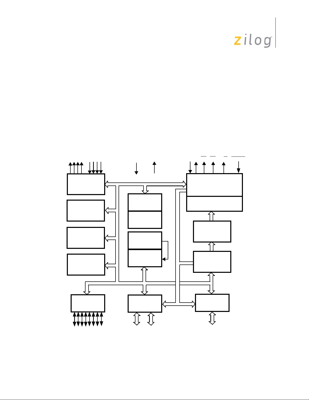
A generalized Z8 CPU block diagram is displayed in Figure 1 on page 2. The same onchip peripherals are used across the MCU product line with the primary differences being
the amount of ROM/RAM, number of I/O lines present, and packaging/temperature
ranges available. This allows code written for one MCU device to be easily ported to
another family member.
Z8® CPU
User Manual
1
Key Features
The key features include:
General-Purpose Register File—Every RAM register acts like an accumulator, speeding
instruction execution and maximizing coding efficiency. Working register groups allow
fast context switching.
Flexible I/O—I/O byte, nibble, and/or bit programmable as inputs or outputs. Outputs are
software programmable as open-drain or push–pull on a port basis. Inputs are SchmittTriggered with autolatches to hold unused inputs at a known voltage state.
Analog Inputs—Three input pins are software programmable as digital or analog inputs.
When in analog mode, two comparator inputs are provided with a common reference
input. These inputs are ideal for a variety of common functions, including threshold level
detection, analog-to-digital conversion, and short circuit detection. Each analog input provides a unique maskable interrupt input.
Timer/Counter—The Timer/Counter (T/C) consists of a programmable 6-bit prescaler and
8-bit downcounter, with maskable interrupt upon end-of-count. Software controls T/C
load/start/stop, countdown read (at any time on the fly), and maskable end-of-count interrupt. Special functions available include T
or external trigger input) and T
clock). These special functions allow accurate hardware input pulse measurement and output waveform generation.
Interrupts—There are six vectored interrupt sources with software-programmable enable
and priority for each of the six sources.
(external counter input, external gate input,
IN
(external access to timer output or the internal system
OUT
Watchdog Timer—An internal Watchdog Timer (WDT) circuit is included as a fail-safe
mechanism so that if software strays outside the bounds of normal operation, the WDT is
used to time-out and reset the MCU. To maximize circuit robustness and reliability, the
UM001604-0108 Z8® CPU Product Overview
Page 9
Z8® CPU
User Manual
default WDT clock source is an internal RC circuit (isolated from the device clock
source).
Auto Reset/Low-Voltage Protection—All family devices have internal Power-On Reset.
ROM devices add low-voltage protection. Low-voltage protection ensures the MCU is in
a known state at all times (in active RUN or RESET modes) without external hardware (or
a device reset pin).
Low-EMI Operation—Mode is programmable via software or as a mask option. This new
option provides for reduced radiated emission via clock and output drive circuit changes.
Low-Power—CMOS with two standby modes; STOP and HALT.
Full Z8® Instruction Set—Forty-eight basic instructions, supported by six addressing
modes with the ability to operate on bits, nibbles, bytes, and words.
2
Output
Port 3
Counter/
Timers (2)
Interrupt
Control
Analog
Comparators
(2)
Port 2
Input
CC
ALU
FLAG
Register
Pointer
Port 0
GND
V
Register File
256 x 8-Bit
XTAL
AS DS
Machine Timing
& Instruction Control
RESET, WDT,
Prg. Memory
512/K x 8-Bit
Program
R/W RESET
POR
Counter
Port 1
8
)
I/O
(
Bit Programmable)
44
Address or I/O
(
Nibble
Programmable)
Address/Data or I/O
(
Byte Programmable
Figure 1. Z8 CPU Block Diagram
UM001604-0108 Z8® CPU Product Overview
Page 10

Product Development Support
The Z8® MCU product line is fully supported with a range of cross assemblers, C compilers, ICEBOX emulators, single and gang OTP/EPROM programmers, and software simulators.
The
Z86CCP01ZEM low-cost Z8 CCP real-time emulator/programmer kit is designed
specifically to support all the products outlined in Tab l e 1 on page 3.
Table 1. Zilog General-Purpose Microcontroller Product Family
Z8® CPU
User Manual
3
RC
Speed
(MHz)
ROM/
Product
Z86C03 512/60 14 1 2 6 F Y Y Y 8 18
Z86E03 512/60 14 1 2 6 F Y N Y 8 18
Z86C04 1K/124 14 2 2 6 F Y Y Y 8 18
Z86E04 1K/124 14 2 2 6 F Y N Y 8 18
Z86C06 1K/124 14 2 2 6 P Y Y Y 12 18
Z86E06 1K/124 14 2 2 6 P Y N Y 12 18
Z86C08 2K/124 14 2 2 6 F Y Y Y 12 18
Z86E08 2K/124 14 2 2 6 F Y N Y 12 18
Z86C30 4K/236 24 2 2 6 P Y Y Y 12 28
Z86E30 4K/236 24 2 2 6 P Y N Y 12 28
Z86C31 2K/124 24 2 2 6 P Y Y Y 8 28
Z86E31 2K/124 24 2 2 6 P Y N Y 8 28
Z86C40 4K/236 32 2 2 6 P Y Y Y 16 40/44
Z86E40 4K/236 32 2 2 6 P Y N Y 16 40/44
Note:
RAM I/O T/C AN INT WDT POR V
Z86Cxx signify ROM devices; 86xx signify EPROM devices; F = fixed; P = programmable.
BO
Pin
Count
The Z86CCP01ZEM kit includes:
•
Z8 CCP evaluation board
•
Z8 CCP power cable
•
Zilog Developer Studio (ZDS) CD-ROM, Including Windows-Based GUI Host Software
•
1999 Zilog Technical Library
•
Z8 CCP User Manual
UM001604-0108 Z8® CPU Product Overview
Page 11

Z8® CPU
User Manual
A Z8 CCP Emulator Accessory Kit (Z8CCP00ZAC) is also available and provides an RS232 cable and power cable along with the 28- and 40- pin ZIF sockets and 28- and 40-pin
target connector cables required to emulate/program 28-/40-pin devices.
4
UM001604-0108 Z8® CPU Product Overview
Page 12

Address Space
Introduction
Z8® CPU includes the following four address spaces:
•
The Z8 Standard Register File contains addresses for peripheral, control, all generalpurpose, and all I/O port registers. This is the default register file specification.
•
The Z8 Expanded Register File (ERF) contains addresses for control and data registers for additional peripherals/features.
•
Z8 external Program Memory contains addresses for all memory locations having
executable code and/or data.
•
Z8 external data memory contains addresses for all memory locations that hold data
only, whether internal or external.
Z8® CPU
User Manual
5
Z8® CPU Standard Register File
The Z8 Standard Register File totals up to 256 consecutive bytes (Registers). The register
file consists of 4 I/O ports (
control registers (
names, locations, and identifiers.
Table 2. Z8 Standard Register File
Hex Address
FF SPL Stack Pointer Low Byte
FE SPH Stack Pointer High Byte
FD RP Register Pointer
FC FLAGS Program Control Flags
FB IMR Interrupt Mask Register
FA IRQ Interrupt Request Register
F9 IPR Interrupt Priority Register
F8 P01M Port 0–1 Mode Register
F7 P3M Port 3 Mode Register
F0h–FFh). Table 2 lists the layout of the register file, including register
Register
Identifier Register Description
00h–03h), 236 General-Purpose Registers (04h–EFh), and 16
F6 P2M Port 2 Mode Register
F5 PRE0 T0 Prescaler
UM001604-0108 Address Space
Page 13

Table 2. Z8 Standard Register File (Continued)
Register
Hex Address
F4 T0 Timer/Counter 0
F3 PRE1 T1 Prescaler
F2 T1 Timer/Counter 1
F1 TMR Timer Mode
F0 SIO Serial I/O
EF R239
General-Purpose Registers (GPR)
04 R4
Identifier Register Description
Z8® CPU
User Manual
6
03 P3 Port 3
02 P2 Port 2
01 P1 Port 1
00 P0 Port 0
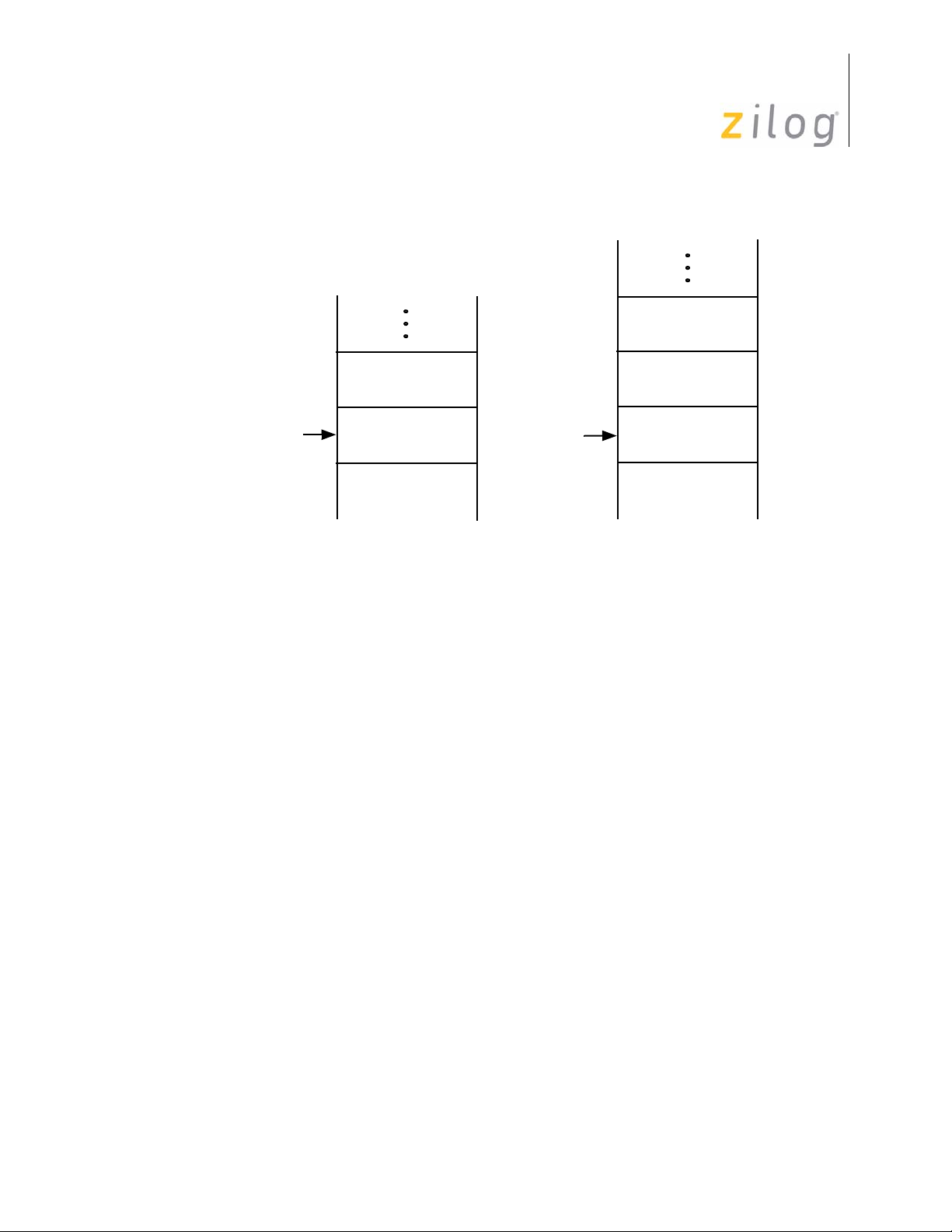
Registers can be accessed as either 8-bit or 16-bit registers using Direct, Indirect, or
Indexed Addressing. All 236 general-purpose registers can be referenced or modified by
any instruction that accesses an 8-bit register, without the requirement for special instructions. Registers accessed as 16 bits are treated as even-odd register pairs (there are 118
valid pairs). In this case, the data’s most significant byte (MSB) is stored in the even numbered register, while the least significant byte (LSB) goes into the next higher odd numbered register. See Figure 2.
MSB
Rn Rn+1
n = Even Address
Figure 2. 16-Bit Register Addressing
LSB
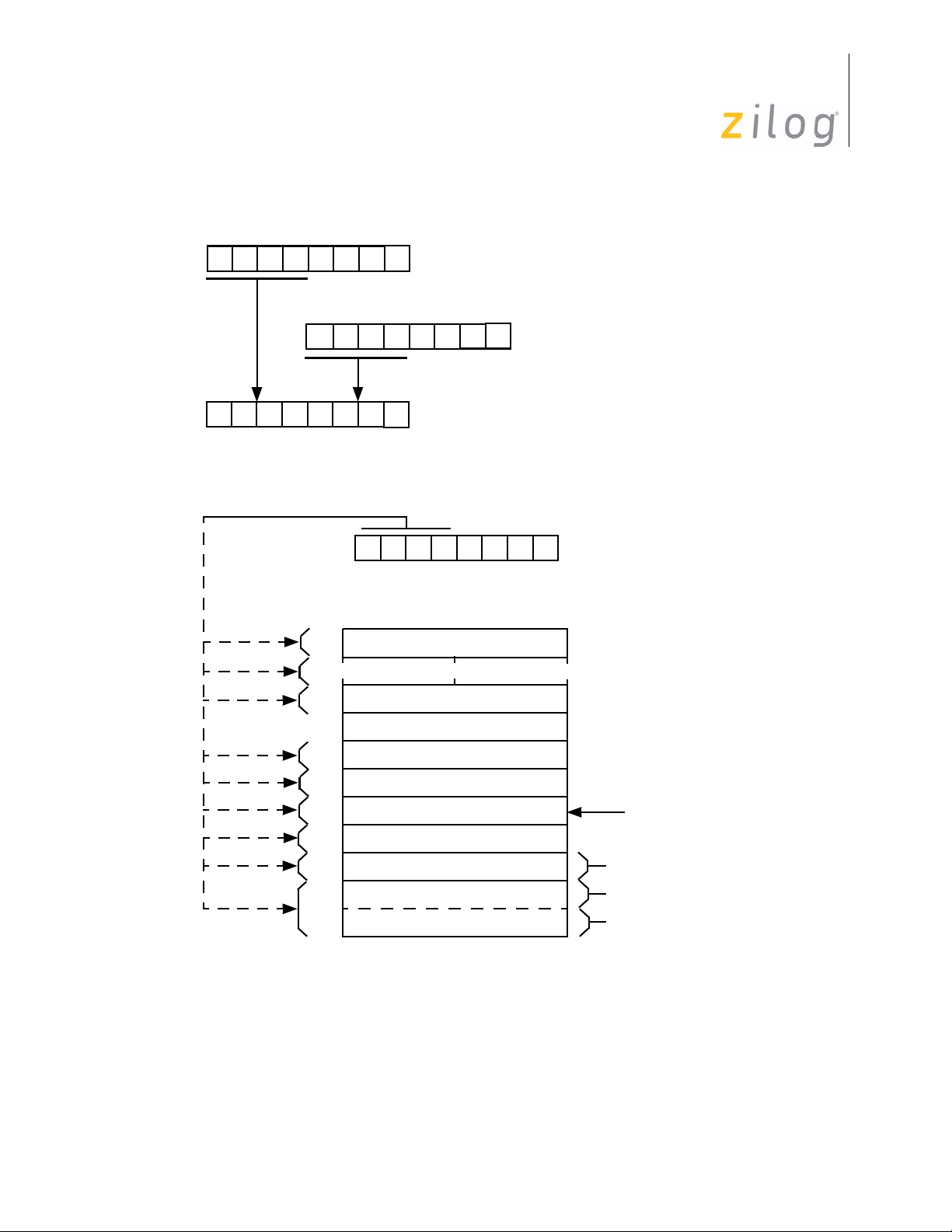
By using a logical instruction and a mask, individual bits within registers can be accessed
for bit set, bit clear, bit complement, or bit test operations. For example, the instruction
AND R15, MASK performs a bit clear operation, Figure 3 on page 7 displays this
example.
UM001604-0108 Address Space
Page 14
Z8® CPU
User Manual
7
0 1 1 1 0 0 0 0
1 1 0 1 1 1 1 1
AND R15, DFh ;Clear Bit 5 of Working Register 15
0 1 0 1 0 0 0 0
Figure 3. Accessing Individual Bits (Example)
When instructions are executed, registers are read when defined as sources and written
when defined as destinations. All General-Purpose Registers function as accumulators,
address pointers, index registers, stack areas, or scratch pad memory.
General-Purpose Registers
General-Purpose Registers are undefined after the device is powered up. The registers
keep their last value after any reset, as long as the reset occurs in the V
specified operating range. It does not keep its last state from a V
below 1.8 V.
R15
MASK
R15
voltage-
CC
reset if VCC drops
LV
Note:
Registers in Bank
E0-EF may only be accessed through the working register and indirect
addressing modes. Direct access cannot be used because the 4-bit working register address
mode already uses the format
number from
0h to Fh.
RAM Protect
The upper portion of the register file address space 80h to EFh (excluding the control registers) may be protected from reading and writing. The RAM Protect bit option is maskprogrammable and is selected by the customer when the ROM code is submitted. After the
mask option is selected, activate this feature from the internal ROM code to turn OFF/on
the RAM Protect by loading either a 0 or 1 into the IMR register, bit D6. A 1 in D6 enables
RAM Protect. Only devices that use registers
Working Register Groups
Z8® instructions can access 8-bit registers and register pairs (16-bit words) using either
4-bit or 8-bit address fields. 8-bit address fields refer to the actual address of the register.
For example, Register
01011000 (58h).
58h is accessed by calling upon its 8-bit binary equivalent,
[E | dst], where dst represents the working register
80h to EFh offer this feature.
UM001604-0108 Address Space
Page 15

Z8® CPU
User Manual
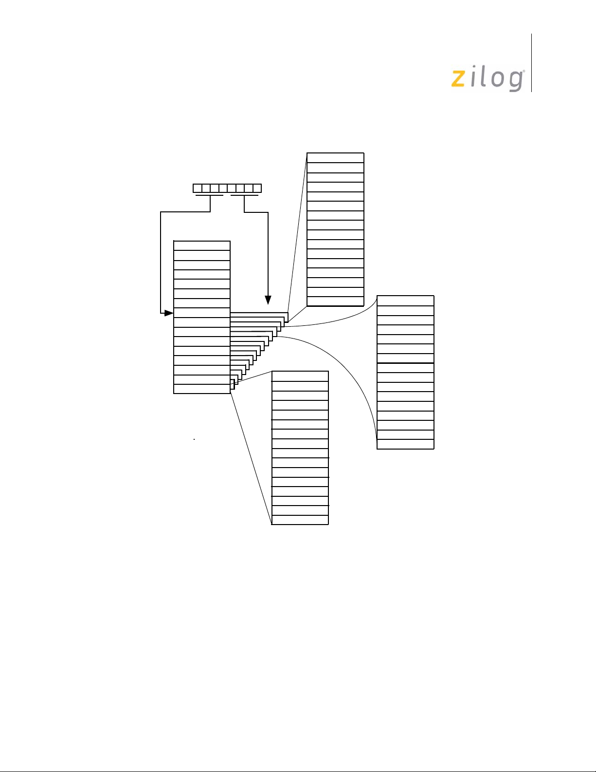
With 4-bit addressing, the register file is logically divided into 16 Working Register
Groups of 16 registers each, as listed in Tab le 3. These 16 registers are known as Working
Registers. A Register Pointer (one of the control registers,
FDh) contains the base address
of the active Working Register Group. The high nibble of the Register Pointer determines
the current Working Register Group.
When accessing one of the Working Registers, the 4-bit address of the Working Register is
combined within the upper four bits (high nibble) of the Register Pointer, thus forming the
8-bit actual address. Figure 4 on page 9 displays this operation. Because working registers
are typically specified by short format instructions, there are fewer bytes of code required,
which reduces execution time. In addition, when processing interrupts or changing tasks,
the Register Pointer speeds context switching. A special Set Register Pointer (SRP)
instruction sets the contents of the Register Pointer.
Table 3. Working Register Groups
8
Register Pointer
(FDh) High Nibble
1111b F F0–FF
1110b E E0–EF
1101b D D0–DF
1100b C C0–CF
1011b B B0–BF
1010b A A0–AF
1001b 9 90–9F
1000b 8 80–8F
0111b 7 70–7F
0110b 6 60–6F
0101b 5 50–5F
0100b 4 40–4F
0011b 3 30–3F
0010b 2 20–2F
0001b 1 10–1F
Working Register
Group (Hex)
Actual Registers
(Hex)
0000b 0 00–0F
UM001604-0108 Address Space
Page 16
Z8® CPU
User Manual
9
0 1 1 1 0 0 0 0
1 1 0 1 1 1 1 1
0 1 1 1 0 1 1 0
Figure 4. Working Register Addressing Examples
R7 R6 R5 R4 R3 R2 R1 R0
The upper nibble of the register file address,
provided by the register pointer, specifies
the active working-register group.
FF
F0
EF
80
7F
70
6F
60
5F
50
4F
40
3F
30
2F
20
1F
10
0F
Working Register Group F
Specified Working Register Group
Working Register Group 1
Working Register Group 0
Register Pointer (FDh), Standard Register File
INC R6 (instruction, short format)
Actual register address (76h)
R253
(Register Pointer)
The lower nibble
of the register
file address
(provided by the
instruction) points
to the specified
register.
R15 to R0
R15 to R4
00
*Note: The full register file is shown. Refer to the selected device product specification for actual file
size.
I/O Ports
R3 to R0
Figure 5. Register Pointer
UM001604-0108 Address Space
Page 17

Error Conditions
Registers in the Z8® Standard Register File must be correctly used because certain conditions produce inconsistent results and should be avoided.
•
Registers F3h and F5h–F9h are write-only registers. If an attempt is made to read
these registers,
•
When register FDh (Register Pointer) is read, the least significant four bits (lower nibble) indicate the current Expanded Register File Bank. (For example,
the Standard Register File, while
•
When Ports 0 and 1 are defined as address outputs, registers 00h and 01h return 1s in
each address bit location when reading.
•
Writing to bits that are defined as timer output, serial output, or handshake output has
no effect.
Z8® CPU
User Manual
10
FFh is returned. Reading any write-only register returns FFh.
0000 indicates
1010 indicates Expanded Register File Bank A.)
•
The Z8 CPU instruction DJNZ uses any general-purpose working register as a counter.
•
Logical instructions such as OR and AND require that the current contents of the
operand be read. They therefore do not function properly on write-only registers.
•
The WDTMR register must be written within the first 60 internal system clocks
(SCLK) of operation after a reset.
Z8 Expanded Register File
The standard register file of the Z8 CPU has been expanded to form 16 Expanded Register
File (ERF) Banks, as displayed in Figure 6 on page 11. Each ERF Bank consists of up to
256 registers (the same amount as in the Standard Register File) that can then be divided
into 16 Working Register Groups. This expansion allows for access to additional feature/
peripheral control and data registers.
UM001604-0108 Address Space
Page 18
Working Register
Group Pointer
Z8 Register File
FF
F0
7F
0F
00
Register Pointer
D7 D6 D5 D4 D3 D2 D1 D0
Expanded Register
Group Pointer
Expanded Register File
Bank (F)
(F) 0F WDTMR
(F) 0E Reserved
(F) 0E Reserved
(F) 0D Reserved
(F) 0C Reserved
(F) 0B SMR
(F) 0A Reserved
(F) 09 Reserved
(F) 08 Reserved
(F) 07 Reserved
(F) 06 Reserved
(F) 05 Reserved
(F) 04 Reserved
(F) 03 Reserved
(F) 02 Reserved
(F) 01 Reserved
(F) 00 PCON
Expanded Register File
Bank (0)
(0) 0F GPR
(0) 0E GPR
(0) 0D GPR
(0) 0C GPR
(0) 0B GPR
(0) 0A GPR
(0) 09 GPR
(0) 08 GPR
(0) 07 GPR
(0) 06 GPR
(0) 05 GPR
(0) 04 GPR
(0) 03 P3
(0) 02 P2
(0) 01 P1
(0) 00 P0
Expanded Register File
Bank (C)
(C) 0F Reserved
(C) 0E Reserved
(C) 0D Reserved
(C) 0C Reserved
(C) 0B Reserved
(C) 0A Reserved
(C) 09 Reserved
(C) 08 Reserved
(C) 07 Reserved
(C) 06 Reserved
(C) 05 Reserved
(C) 04 Reserved
(C) 03 Reserved
(C) 02 SCON
(C) 01 RXBUF
(C) 00 SCOMP
Z8® CPU
User Manual
11
*Note: The fully implemented register file is shown. Refer to the specific product specification for actual register file architecture implemented.
Figure 6. Expanded Register File Architecture
Currently, three out of the possible sixteen Z8 ERF Banks have been implemented. ERF
®
Bank 0, also known as the Z8
played in Figure 7 on page 12. Only Working Register Group 0 (register addresses
Standard Register File, has all 256 bytes defined, as dis-
00h to
0Fh) has been defined for ERF Bank C and ERF Bank F (see Table 4 on page 12). All
other working register groups in ERF Banks C and F, as well as the remaining thirteen
ERF Banks, are not implemented. All are reserved for future use.
UM001604-0108 Address Space
Page 19

Z8® CPU
User Manual
12
When an ERF Bank is selected, register addresses 00h to 0Fh access those sixteen ERF
Bank registers—in effect replacing the first sixteen locations of the Z8
®
Standard Register
File.
For example, if ERF Bank C is selected, the Z8 Standard Registers
no longer accessible. Registers
00h through 0Fh are now the 16 registers from ERF Bank
00h through 0Fh are
C, Working Register Group 0. No other Z8 Standard Registers are affected because only
Working Register Group 0 is implemented in ERF Bank C.
Access to the ERF is accomplished through the Register Pointer (
FDh). The lower nibble
of the Register Pointer determines the ERF Bank while the upper nibble determines the
Working Register Group within the register file, as displayed in Figure 7.
0 1 1 1
Working
Register
Group
Select ERF Bank Ch
Working Register Group 7h
Figure 7. Register Pointer Example
1 1 0 0
Expanded
Register
Bank
The value of the lower nibble in the Register Pointer (
FDh) corresponds to the ERF Bank
identification. Table 4 lists the lower nibble value and the register file assigned to it.
Table 4. ERF Bank Address
Register Pointer
(FDh) Low Nibble
0000b 0 Z8 Standard Register File*
0001b 1 Expanded Register File Bank 1
0010b 2 Expanded Register File Bank 2
0011b 3 Expanded Register File Bank 3
0100b 4 Expanded Register File Bank 4
0101b 5 Expanded Register File Bank 5
0110b 6 Expanded Register File Bank 6
0111b 7 Expanded Register File Bank 7
1000b 8 Expanded Register File Bank 8
Hex
Register File
UM001604-0108 Address Space
Page 20

Table 4. ERF Bank Address (Continued)
Register Pointer
(FDh) Low Nibble
1001b 9 Expanded Register File Bank 9
1010b A Expanded Register File Bank A
1011b B Expanded Register File Bank B
1100b C Expanded Register File Bank C
1101b D Expanded Register File Bank D
1110b E Expanded Register File Bank E
1111b F Expanded Register File Bank F
*
The Z8® Standard Register File is equivalent to Expanded Register File
Bank 0.
Hex
Register File
Z8® CPU
User Manual
13
The upper nibble of the register pointer selects which group of 16 bytes in the Register
File, out of the 256 total bytes, is accessed as working registers. Table 5 lists an example.
Table 5. Register Pointer Access Example
R253 RP = 00h ;ERF Bank 0, Working Reg.
Group 0
R0 = Port 0 = 00h
R1 = Port 1 = 01h
R2 = Port 2 = 02h
R3 = Port 3 = 03h
R11 = GPR 0Bh
R15 = GPR 0Fh
If R253 RP = 0Fh ;ERF Bank F, Working Reg.
Group 0
R0 = PCON = 00h
R1 = Reserved = 01h
R2 = Reserved = 02h
R11 = SMR = 0Bh
R15 = WDTMR = 0Fh
UM001604-0108 Address Space
Page 21

Table 5. Register Pointer Access Example (Continued)
If R253 RP = FFh
;ERF Bank F, Working Reg.
Group F.
00h = PCON
R0 = SI0 01h = Reserved
R1 = TMR 02h = Reserved
...
R2 = T1 0Bh = SMR
...
R15 = SPL 0Fh = WDTMR
Z8® CPU
User Manual
14
Because enabling an ERF Bank (C or F) only changes register addresses 00h to 0Fh, the
working register pointer can be used to access either the selected ERF Bank (Bank C or F,
Working Register Group 0) or the
®
Z8
Standard Register File (ERF Bank 0, Working Reg-
ister Groups 1 through F).
When an ERF Bank other than Bank 0 is enabled, the first 16 bytes of
the Z8 Standard
Register File (I/O ports 0 to 3, Groups 4 to F) are no longer accessible (the selected ERF
Bank, Registers
00h to 0Fh are accessed instead). It is important to re-initialize the Regis-
ter Pointer to enable ERF Bank 0 when these registers are required for use.
The SPI register is mapped into ERF Bank C. Access is easily done using the example in
Table 6.
Table 6. ERF Bank C Access Example
LD RP, #0Ch ;Select ERF Bank C working
;register group 0 for access.
LD R2,#xx ;access SCON
LD R1, #xx ;access RXBUF
LD RP, #00h ;Select ERF Bank 0 so I/O ports
;are again accessible.
UM001604-0108 Address Space
Page 22

Z8® CPU
User Manual
Table 7. Z8 ERF Bank Layout
ERF Bank ERF
Fh PCON, SMR, WDT, (00h, 0Bh, 0Fh), Working Register Group 0 only
implemented.
Eh Not implemented (reserved)
Dh Not implemented (reserved)
Ch SPI Registers: SCOMP, RXBUF, SCON (00h, 01h, 02h), Working
Register Group 0 only implemented.
Bh Not implemented (reserved)
Ah Not implemented (reserved)
9h Not implemented (reserved)
15
8h Not implemented (reserved)
7h Not implemented (reserved)
6h Not implemented (reserved)
5h Not implemented (reserved)
4h Not implemented (reserved)
3h Not implemented (reserved)
2h Not implemented (reserved)
1h Not implemented (reserved)
0h Z8 Ports 0, 1, 2, 3, and General-Purpose Registers 04h to EFh, and
control registers F0h to FFh.
Refer to the specific product specification to determine the above registers are implemented.
Z8® Control and Peripheral Registers
Standard Z8 Registers
The standard Z8 control registers govern the operation of the CPU. Any instruction which
references the register file can access these control registers. The following control registers are available:
•
Interrupt Priority Register (IPR)
•
Interrupt Mask Register (IMR)
•
Interrupt Request Register (IRQ)
UM001604-0108 Address Space
Page 23

Z8® CPU
User Manual
•
Program Control Flags (FLAGS)
•
Register Pointer (RP)
•
Stack Pointer High-Byte (SPH)
•
Stack Pointer Low-Byte (SPL)
The Z8
program instructions. The PC is not an addressable register.
Peripheral registers are used to transfer data, configure the operating mode, and control the
operation of the on-chip peripherals. Any instruction that references the register file can
access the peripheral registers. The peripheral registers are:
•
•
®
CPU uses a 16-bit Program Counter (PC) to determine the sequence of current
Serial I/O (SIO)
Timer Mode (TMR)
16
•
Timer/Counter 0 (T0)
•
T0 Prescaler (PRE0)
•
Timer/Counter 1 (T1)
•
T1 Prescaler (PRE1)
•
Port 0–1 Mode (P01M)
•
Port 2 Mode (P2M)
•
Port 3 Mode (P3M)
In addition, the four port registers (P0–P3) are considered to be peripheral registers.
Expanded Z8 Registers
The expanded Z8 control registers govern the operation of additional features or peripherals. Any instruction which references the register file can access these registers.
The ERF contains the control registers for WDT, Port Control, Serial Peripheral Interface
(SPI), and the SMR functions. Figure 6 on page 11 displays the layout of the Register
Banks in the ERF. Register Bank C in the ERF consists of the registers for the SPI. Ta b l e 8
lists the registers within ERF Bank C, Working Register Group 0.
Table 8. ERF Bank C WR Group 0
Register Function Working Register
F Reserved R15
E Reserved R14
D Reserved R13
UM001604-0108 Address Space
Page 24

Table 8. ERF Bank C WR Group 0 (Continued)
Register Function Working Register
C Reserved R12
B Reserved R11
A Reserved R10
9 Reserved R9
8 Reserved R8
7 Reserved R7
6 Reserved R6
5 Reserved R5
4 Reserved R4
Z8® CPU
User Manual
17
3 Reserved R3
2 SPI Control (SCON) R2
1 SPI Tx/Rx Data (Roxburgh) R1
0 SPI Compare (SCOMP) R0
Working Register Group 0 in ERF Bank 0 consists of the registers for Z8® General-Purpose Registers and ports. Table 9 lists the registers within this group.
Table 9. ERF Bank 0 WR Group 0
Register Function Working Register
F General-Purpose Register R15
E General-Purpose Register R14
D General-Purpose Register R13
C General-Purpose Register R12
B General-Purpose Register R11
A General-Purpose Register R10
9 General-Purpose Register R9
8 General-Purpose Register R8
7 General-Purpose Register R7
6 General-Purpose Register R6
5 General-Purpose Register R5
UM001604-0108 Address Space
Page 25

Z8® CPU
User Manual
Table 9. ERF Bank 0 WR Group 0 (Continued)
Register Function Working Register
4 General-Purpose Register R4
3Port 3 R3
2Port 2 R2
1Port 1 R1
0Port 0 R0
Working Register Group 0 in ERF Bank F consists of the control registers for STOP mode,
WDT, and port control. Table 10 lists the registers within this group.
Table 10. ERF Bank F WR Group 0
18
Register Function Working Register
F WDTMR R15
E Reserved R14
D Reserved R13
C Reserved R12
BSMR R11
A Reserved R10
9 Reserved R9
8 Reserved R8
7 Reserved R7
6 Reserved R6
5 Reserved R5
4 Reserved R4
3 Reserved R3
2 Reserved R2
1 Reserved R1
0PCON R0
UM001604-0108 Address Space
Page 26

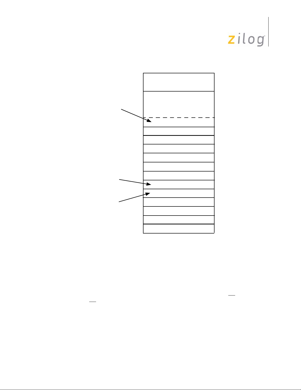
Program Memory
The first 12 bytes of Program Memory are reserved for the interrupt vectors, as displayed
in Figure 8 on page 20. These locations contain six 16-bit vectors that correspond to the
six available interrupts. Address 12 up to the maximum ROM address consists of on-chip
mask-programmable ROM. Refer to the product data sheet for the exact program, data,
register memory size, and address range available. At addresses outside the internal ROM,
®
the Z8
Address/Data mode for devices with Port 0 and Port 1 featured. Otherwise, the program
counter continues to execute NOPs up to address
to fetch executable code (see Figure 8).
The internal Program Memory is one-time programmable (OTP) or mask programmable
dependent on the specific device. A ROM protect feature prevents dumping of the ROM
contents by inhibiting execution of the LDC, LDCI, LDE, and LDEI instructions to Program Memory in all modes. ROM look-up tables cannot be used with this feature.
CPU executes external Program Memory fetches through Port 0 and Port 1 in
Z8® CPU
User Manual
19
FFFFh, roll over to 0000h, and continue
The ROM Protect option is mask-programmable, to be selected when the ROM code is
submitted. For the OTP ROM, the ROM Protect option is an OTP programming option.
UM001604-0108 Address Space
Page 27
Location of
First Byte of
Instruction
Executed
After RESET
65535
4096
4095
12
External
ROM and RAM
On–Chip
ROM
Z8® CPU
User Manual
20
Interrupt
Vector
(Lower Byte)
Interrupt
Vector
(Upper Byte)
Figure 8. Z8® Program Memory Map
Z8® External Memory
Z8 CPU, in some cases, has the capability to access external Program Memory with the
16-bit Program Counter. To access external Program Memory the Z8 CPU offers multiplexed address/data lines (AD7–AD0) on Port 1 and address lines (A15–A8) on Port 0.
This feature only applies to devices that offer Port 0 and Port 1. The maximum external
address is
Strobe), DS
Memory starts after the last address of the internal ROM. Figure 9 on page 21 displays an
example of external Program Memory for the Z8 CPU.
FFFF. This memory interface is supported by the control lines AS (Address
(Data Strobe), and R/W (Read/Write). The origin of the external Program
11
10
9
8
7
6
5
4
3
2
0
IRQ
5
IRQ
5
IRQ
4
IRQ
4
IRQ
3
IRQ
3
IRQ
2
IRQ
2
IRQ
1
IRQ
1
1
IRQ
IRQ
0
0
UM001604-0108 Address Space
Page 28

External Data Memory
The Z8 CPU, in some cases, can address up to 60 KB of external data memory beginning
at location 4096. External data memory (DM
external Program Memory space. DM
appear on pin P34, is used to distinguish between data and Program Memory space. The
state of the DM
opcode references Program Memory (DM
data memory (DM
and D4 for this mode.
signal is controlled by the type of instruction being executed. An LDC
active Low). You must configure Port 3 Mode Register (P3M) bits D3
65535
Z8® CPU
User Manual
21
) can be included with, or separated from, the
, an optional I/O function that can be programmed to
inactive), and an LDE instruction references
External
Memory
4096
4095
Not Addressable
0
*Note: For additional information on using external memory, see Chapter 10 of this
manual. For exact memory addressing options available, see the device product
specification.
Figure 9. External Memory Map
UM001604-0108 Address Space
Page 29

Z8® Stacks
Stack operations can occur in either the Z8 Standard Register File or external data memory. Under software control, Port 0–1 Mode register (
the General-Purpose Registers can be used for the stack when the internal stack is
selected.
Z8® CPU
User Manual
22
F8h) selects the stack location. Only
The register pair
operations. The stack address is stored with the MSB in
FEh and FFh form the 16-bit Stack Pointer (SP), that is used for all stack
FEh and LSB in FFh, see
Figure 10.
FFh
LOWER Byte
FEh
UPPER Byte
Figure 10. Stack Pointer
Stack Pointer Low
Stack Pointer High
The stack address is decremented prior to a PUSH operation and incremented after a POP
operation. The stack address always points to the data stored on the top of the stack. The
Z8 CPU stack is a return stack for CALL instructions and interrupts, as well as a data
stack.
During a CALL instruction, the contents of the PC are saved on the stack. The PC is
restored during a RETURN instruction. Interrupts cause the contents of the PC and Flag
registers to be saved on the stack. The IRET instruction restores them (see Figure 11 on
page 23).
When the Z8 CPU is configured for an internal stack (using the Z8 Standard Register
File), register
FFh serves as the Stack Pointer. The value in FEh is ignored. FEh can be
used as a general-purpose register in this case only.
An overflow or underflow can occur when the stack address is incremented or decremented during normal stack operations. The programmer must prevent this occurrence, or
unpredictable operation happens.
UM001604-0108 Address Space
Page 30
PCL
Z8® CPU
User Manual
23
Top of Stack
PCL
PCH
Stack Contents
After a Call
Instruction
Top of Stack
Figure 11. Stack Operations
PCH
FLAGS
Stack Contents
After an
Interrupt Cycle
UM001604-0108 Address Space
Page 31

Clock
Frequency Control
Z8® CPU
User Manual
24
Z8® CPU derives its timing from on-board clock circuitry connected to pins XTAL1 and
XTAL2. The clock circuitry consists of an oscillator, a divide-by-two shaping circuit, and
a clock buffer. Figure 12 displays the clock circuitry. The oscillator’s input is XTAL1 and
its output is XTAL2. The clock can be driven by a crystal, a ceramic resonator, LC clock,
RC, or an external clock source.
In some cases, the Z8 CPU has an EPROM/OTP option or a Mask ROM option bit to
bypass the divide-by-two flip flop in Figure 12. This feature is used in conjunction with
the low EMI option. When low EMI is selected, the device output drive and oscillator
drive is reduced to approximately 25 percent of the standard drive and the divide-by-two
flip flop is bypassed such that the XTAL clock frequency is equal to the internal system
clock frequency. In this mode, the maximum frequency of the XTAL clock is 4 MHz.
Refer to specific product specification for availability of options and output drive characteristics.
Clock Control
In some cases, the Z8 CPU offers software control of the internal system clock via programming register bits. The bits are located in the Stop Mode Recovery Register in
Expanded Register File Bank F, Register
and determines the mode of Stop Mode Recovery (see Figure 13 on page 25). Refer to the
specific product specification for availability of this feature/register.
XTAL1
XTAL2
OSC
Figure 12. Z8® CPU Clock Circuit
÷2
Buffer
0Bh. This register selects the clock divide value
Internal
Clock
UM001604-0108 Clock
Page 32

Z8® CPU
User Manual
SMR (F) OB
D7 D6 D5 D4 D3 D2 D1 D0
SCLK ÷ TCLK Divide by 16
0 OFF **
1 ON
External Clock Divide Mode by 2
0 = SCLK ÷ TCLK = XTAL ÷ 2*
* Default setting after RESET.
**Default setting after RESET and Stop Mode Recovery.
Figure 13. Stop Mode Recovery Register (Write-Only Except D7, Which is Read-Only)
1 = SCLK ÷ TCLK = XTAL
SCLK ÷ TCLK Divide-By-16 Select
25
The D0 bit of the SMR controls a divide-by-16 prescaler of SCLK ÷ TCLK. The purpose
of this control is to selectively reduce device power consumption during normal processor
execution (SCLK control) and/or HALT mode (where TCLK sources counter/timers and
interrupt logic).
External Clock Divide-By-Two
The D1 bit can eliminate the oscillator divide-by-two circuitry. When this bit is 0, SCLK
(System Clock) and TCLK (Timer Clock) are equal to the external clock frequency
divided by two. The SCLK ÷ TCLK is equal to the external clock frequency when this bit
is set (D1 = 1). Using this bit, together with D7 of PCON, further helps lower EMI (D7
(PCON) = 0, D1 (SMR) = 1). The default setting is 0. Maximum frequency is 4 MHz with
D1 = 1 (see Figure 14 on page 26).
UM001604-0108 Clock
Page 33

D1 (SMR)
D0 (SMR)
Z8® CPU
User Manual
26
OSC
÷2
Oscillator Control
In some cases, the Z8® CPU offers software control of the oscillator to select low EMI
drive or standard drive. The selection is done by programming bit D7 of the Port Configuration (PCON) register (see Figure 15 on page 26). The PCON register is located in
Expanded Register File Bank F, Register
A 1 in bit D7 configures the oscillator with standard drive, while a 0 configures the oscillator with Low EMI drive. This only affects the drive capability of the oscillator and does
not affect the relationship of the XTAL clock frequency to the internal system clock
(SCLK).
PCON (Fh) 00h
D7 D6 D5 D4 D3 D2 D1 D0
÷16
External Clock
Figure 14. External Clock Circuit
00h.
Low EMI Oscillator
0 Low EMI
1 Standard
Figure 15. Port Configuration Register (Write-Only)
UM001604-0108 Clock
Page 34

Oscillator Operation
The Z8® CPU uses a Pierce oscillator with an internal feedback (see Figure 16). The
advantages of this circuit are low cost, large output signal, low-power level in the crystal,
stability with respect to V
affects).
One drawback is the requirement for high gain in the amplifier to compensate for feedback
path losses. The oscillator amplifies its own noise at start-up until it settles at the frequency that satisfies the gain/phase requirements A x B = 1, where A = V
the amplifier and B = V
around the loop is forced to zero (360 degrees). Because VIN must be in phase with itself,
the amplifier/inverter provides 180 degree phase shift and the feedback element is forced
to provide the other 180 degrees of phase shift.
R1 is a resistive component placed from output to input of the amplifier. The purpose of
this feedback is to bias the amplifier in its linear region and to provide the start-up transition.
Z8® CPU
User Manual
and temperature, and low impedances (not disturbed by stray
CC
/VI is the gain of
0
/V0 is the gain of the feedback element. The total phase shift
I
27
Capacitor C
combined with the amplifier output resistance provides a small phase shift. It
2
also provides some attenuation of overtones.
Capacitor C
C
and C2 can affect the start-up time if they increase dramatically in size. As C1 and C2
1
combined with the crystal resistance provides additional phase shift.
1
increase, the start-up time increases until the oscillator reaches a point where it does not
start up any more.
For fast and reliable oscillator start-up over the manufacturing process range, Zilog
®
recommends that the load capacitors be sized as low as possible without resulting in overtone
operation.
XTAL1
Z8 CPU
A
RI
V
1
C1
V
0
XTAL2
C2
V
SS
Figure 16. Pierce Oscillator with Internal Feedback Circuit
UM001604-0108 Clock
Page 35

Layout
Z8® CPU
User Manual
Traces connecting crystal, caps, and the Z8® CPU oscillator pins should be as short and
wide as possible. This reduces parasitic inductance and resistance. The components (caps,
crystal, resistors) should be placed as close as possible to the oscillator pins of the Z8
CPU.
The traces from the oscillator pins of the IC and the ground side of the lead caps should be
guarded from all other traces (clock, V
cross talk and noise injection. This is usually accomplished by keeping other traces and
system ground trace planes away from the oscillator circuit and by placing a Z8 CPU
device V
lead caps should be connected to a single trace to the Z8 CPU’s V
not be shared with any other system ground trace or components except at the Z8 CPU’s
V
pin. This is to prevent differential system ground noise injection into the oscillator
SS
(see Figure 17 on page 29).
ground ring around the traces/components. The ground side of the oscillator
SS
, address/data lines, system ground) to reduce
CC
(GND) pin. It should
SS
28
Indications of an Unreliable Design
Start-up time and output level are two major indicators that are used in working designs to
determine their reliability over full lot and temperature variations. These two indicators
are described below.
Start-Up Time—If start-up time is excessive, or varies widely from unit to unit, there is
probably a gain problem. C1/C2 must be reduced; the amplifier gain is not adequate at frequency, or crystal resistance is too large.
Output Level—The signal at the amplifier output should swing from ground to V
This indicates there is adequate gain in the amplifier. As the oscillator starts up, the signal
amplitude grows until clipping occurs, at which point the loop gain is effectively reduced
to unity and constant oscillation is achieved. A signal of less than 2.5 V peak-to-peak is an
indication that low gain may be a problem. Either C
low-resistance crystal should be used.
Circuit Board Design Rules
The following circuit board design rules are suggested:
•
To prevent induced noise the crystal and load capacitors should be physically located
as close to the Z8 CPU as possible.
•
Signal lines should not run parallel to the clock oscillator inputs. In particular, the
crystal input circuitry and the internal system clock output should be separated as
much as possible.
CC
or C2 should be made smaller or a
1
.
•
VCC power lines should be separated from the clock oscillator input circuitry.
•
Resistivity between XTAL1 or XTAL2 and the other pins should be greater than 10
MΩ.
UM001604-0108 Clock
Page 36

C1
C2
XTAL1
Z8 CPU
XTAL2
V
SS
20 mm
max
User Manual
Signal Line
Layout Should
Avoid High
Lighted Areas
Z8® CPU
29
Clock Generator Circuit
Signals A B
(Parallel Traces
Must Be Avoided)
Signal C
2
Z8 CPU
3
(Connection to System Group
Must Be Avoided)
Figure 17. Circuit Board Design Rules
Crystals and Resonators
Crystals and ceramic resonators, displayed in Figure 18 should have the characteristics
listed in Table 11 to ensure proper oscillator operation.
1
2
3
®
Z8
CPU
V
SS
Board Design Example
(Top View)
Table 11. Crystal/Resonator Characteristics
Crystal Cut AT (crystal only)
Mode Parallel, Fundamental mode
Crystal Capacitance < 7 pF
Load Capacitance 10 pF < CL < 220 pF, 15 typical
Resistance 100 Ω max
UM001604-0108 Clock
Page 37

Z8® CPU
User Manual
Depending on operation frequency, the oscillator may require the addition of capacitors
C1 and C2 (displayed in Figure 18). The capacitance values are dependent on the manufacturer’s crystal specifications.
V
SS
Z8® CPU
XTAL1
XTAL2
30
RF
C1
R
C2
D
Figure 18. Crystal/Ceramic Resonator Oscillator
XTAL1
C1
C2
L
Z8® CPU
XTAL2
V
SS
Figure 19. LC Clock
In most cases, the R
ceramic resonator manufacturer. The R
is 0 Ω and RF is infinite. It is determined and specified by the crystal/
D
can be increased to decrease the amount of drive
D
from the oscillator output to the crystal. It can also be used as an adjustment to avoid clipping of the oscillator signal to reduce noise. The R
the crystal/ceramic resonator. The Z8
®
oscillator already has an internal shunt resistor in
can be used to improve the start-up of
F
parallel to the crystal/ceramic resonator.
UM001604-0108 Clock
Page 38

XTAL1
Z8® CPU
User Manual
31
Note:
Z8® CPU
XTAL2
Figure 20. External Clock
V
SS
In Figure 18 through Figure 20, Zilog® recommends that you connect the load capacitor
ground trace directly to the V
(GND) pin of the Z8® CPU to ensure that no system noise
SS
is injected into the Z8 clock. This trace should not be shared with any other components
except at the V
pin of the Z8 CPU.
SS
In some cases, the Z8 CPU’s XTAL1 pin also functions as one of the EPROM high-voltage mode programming pins or as a special factory test pin. In this case, applying 2 V
above V
on the XTAL1 pin causes the device to enter one of these modes. Because this
CC
pin accepts high voltages to enter these respective modes, the standard input protection
diode to V
is exposed to much system noise, a diode from XTAL1 to V
is not on XTAL1. Zilog recommends that in applications where the Z8 CPU
CC
be used to prevent acciden-
CC
tal enabling of these modes. This diode does not affect the crystal/ceramic resonator operation.
A parallel resonant crystal or resonator data sheet specifies a load capacitor value that is
the series combination of C
and C2, including all parasitics (PCB and holder).
1
LC Oscillator
The Z8 CPU oscillator can use a LC network to generate a XTAL clock (see Figure 19 on
page 30).
The frequency stays stable over V
mined by following equation.
Frequency
1
--------------------------------------=
2π LCT()
12⁄
where L is the total inductance including parasitics and C
including the parasitics.
UM001604-0108 Clock
and temperature. The oscillation frequency is deter-
CC
is the total series capacitance
T
Page 39

Simple series capacitance is calculated using the following equation:
Z8® CPU
User Manual
32
1
=
C
C
T
If C1 = C
1 = 2
C
= C
T
C1 = 2C
Sample calculation for capacitance C
value of 27 µH.
5.83 (106) =
C
= 27.6 pF
T
Therefore, C
RC Oscillator
In some cases, the Z8® CPU features an RC oscillator option. Refer to the specific product
specification for availability. The RC oscillator requires a resistor across XTAL1 and
XTAL2. An additional load capacitor is required from the XTAL1 input to V
Figure 21.
1
1
+
C
1
2
1
2
T
1
2π [2.7 (10
= 55.2 pF and C2 = 55.2 pF.
1
–6
) CT] 1/2
and C2 of 5.83 MHz frequency and inductance
1
pin, see
SS
XTAL1
R
C1
Z8® CPU
XTAL2
V
SS
Figure 21. RC Clock
UM001604-0108 Clock
Page 40

Reset
Z8® CPU
User Manual
This section describes the Z8® CPU reset conditions, reset timing, and register initialization procedures. Reset is generated by Power-On Reset (POR), Reset Pin, Watchdog
Timer (WDT), and Stop Mode Recovery.
A system reset overrides all other operating conditions and puts the Z8 CPU into a known
state. To initialize the chip’s internal logic, the RESET
21 SCP or 5 XTAL clock cycles. The control register and ports are reset to their default
conditions after a POR, a reset from the RESET
mode and HALT mode. The control registers and ports are not reset to their default conditions after Stop Mode Recovery and WDT time-out while in STOP mode.
input must be held Low for at least
pin, or WDT time-out while in RUN
33
While RESET
remains High. The program counter is loaded with 000Ch. I/O ports and control reg-
R/W
isters are configured to their default reset state.
Resetting the Z8 CPU does not affect the contents of the general-purpose registers.
pin is Low, AS is output at the internal clock rate, DS is forced Low, and
Reset Pin, Internal POR Operation
In some cases, the Z8 CPU hardware RESET pin initializes the control and peripheral registers, as listed in Table 12 on page 34 through Table 15 on page 37. Specific reset values
are shown by 1 or 0, while bits whose states are unknown are indicated by the letter U.
Table 12 on page 34 through Table 15 on page 37 list the reset conditions for the Z8 CPU.
Note:
The register file reset state is device dependent. Refer to the selected device product specifications for register availability and reset state.
UM001604-0108 Reset
Page 41

Table 12. Sample Control and Peripheral Register Reset Values (ERF Bank 0)
Z8® CPU
User Manual
34
Register
(Hex) Register Name
F0 Serial I/O UUUUUUUU
F1 Timer Mode 00000000Counter/Timers stopped.
F2 Counter/Timer1 UUUUUUUU
F3 T1 Prescaler UUUUUU0 0Single-pass count mode,
F4 Counter/Timer0 UUUUUUUU
F5 T0 Prescaler UUUUUUU0Single-pass count mode.
F6 Port 2 Mode 11111111All inputs.
F7 Port 3 Mode 00000000Port 2 open-drain, P33–P30
F8 Port 0–1 Mode 01001101Internal Stack, Normal Memory
F9 Interrupt Priority UUUUUUUU
FA Interrupt Request 00000000All Interrupts Cleared.
FB Interrupt Mask 0UUUUUUUInterrupts Disabled.
FC Flags UUUUUUUU
Bits
Comments76543210
external clock source.
Input, P37–P34 Output.
Timing.
FD Register Pointer 00000000
FE Stack Pointer (High) UUUUUUUU
FF Stack Pointer (Low) UUUUUUUU
Program execution starts 5 to 10 clock cycles after internal RESET has returned High. The
initial instruction fetch is from location
000Ch. Figure 22 on page 35 displays reset tim-
ing.
UM001604-0108 Reset
Page 42
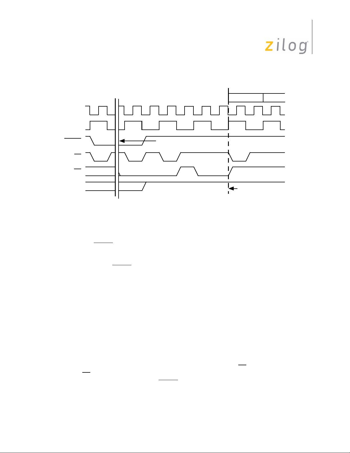
Clock
SCLK
Z8® CPU
User Manual
35
First Machine Cycle
T1
RESET
AS
DS
R/W
Hold Low For 4 SCLK
Periods (Minimum)
First Instruction Fetch
Figure 22. Reset Timing
After a reset, the first routine executed should be one that initializes the control registers to
the required system configuration.
The RESET
pin is the input of a Schmitt-Triggered circuit. Resetting the Z8® CPU initializes port and control registers to their default states. To form the internal reset line, the output of the trigger is synchronized with the internal clock. The clock must therefore be
running for RESET
to function. It requires 4 internal system clocks after reset is detected
for the Z8 CPU to reset the internal circuitry. An internal pull-up, combined with an external capacitor of 1
µF, provides enough time to properly reset the Z8 CPU (see Figure 23 on
page 36). In some cases, the Z8 CPU has an internal POR timer circuit that holds the Z8
CPU in reset mode for a duration (T
) before releasing the device out of reset. On these
POR
Z8 devices, the internally generated reset drives the reset pin low for the POR time. Any
devices driving the reset line must be open-drained in order to avoid damage from possible
conflict during reset conditions. This reset time allows the on-board clock oscillator to stabilize.
To avoid asynchronous and noisy reset problems, the Z8 CPU is equipped with a reset filter of four external clocks (4TpC). If the external reset signal is less than 4TpC in duration,
no reset occurs. On the fifth clock after the reset is detected, an internal RST signal is
latched and held for an internal register count of 18 external clocks, or for the duration of
the external reset, whichever is longer. During the reset cycle, DS
cycles at a rate of the internal system clock. Program execution begins at location
AS
000Ch, 5-10 TpC cycles after RESET is released. For the internal Power-On Reset, the
reset output time is specified as T
. Refer to specific product specifications for actual
POR
is held active low while
values.
UM001604-0108 Reset
Page 43

+5V
100 KΩ
to
200 KΩ
1 K
RESET
1 µF
10 V
Figure 23. Example of External Power-On Reset Circuit
Z8® CPU
User Manual
36
Table 13. ERF Bank 0 Reset Values at RESET
Register
(Hex) Register Name
00 Port 0 UUUUUUUUInput mode, output set to push–pull.
01 Port 1 UUUUUUUUInput mode, output set to push–pull.
02 Port 2 UUUUUUUUInput mode, output set to open
03 Port 3 1111UUUUStandard digital input and output
04–EF General-Purpose
UUUUUUUUUndefined.
Registers 04h–EFh
Table 14. Sample Expanded Register File Bank C Reset Values
Register
(Hex) Register Name
Bits
Comments76543210
drain.
Z86L7X Family Device Port P34P37 = 0
(Except Z86L70/71/75)
All other Z8 = 1.
Bits
Comments76543210
00 SPI Compare (SCOMP) 00000000
01 Receive Buffer (RxBUF) U U U U U U U U
02 SPI Control (SCON) U U U U 0 0 0 0
UM001604-0108 Reset
Page 44

Table 15. Sample Expanded Register File Bank F Reset Values
Z8® CPU
User Manual
37
Register
(Hex) Register Name
00 Port Configuration
(PCON)
0B Stop Mode
Recovery (SMR)
0F Watchdog Timer
Mode (WDTMR)
Bits
Comments76543210
11111110Comparator outputs disabled on Port 3.
Port 0 and 1 output is push–pull.
Port 0, 1, 2, 3, and oscillator with
standard output drive.
00100000Clock divide by 16 off.
XTAL divide by 2.
POR and/OR External Reset.
Stop delay on.
Stop recovery level is low, STOP Flag
is POR.
UUU01101512 TPC for WDT time out, WDT runs
during STOP.
UM001604-0108 Reset
Page 45

Z8® CPU
User Manual
38
RESET
WDT Select
(WDTMR)
CLK Source
Select (WDTMR)
XTAL
VDD
2.6V REF
WDT
.
From Stop Mode
Recovery Source
4 Clock
Filter
RC
OSC.
2.6 V Operating
Voltage Det.
+
-
Clear 18 Clock RESET RESET
CLK Generator
WDT TAP SELECT
256 TpC 256 512 1024 4096
M
POR TpC TpC TpC TpC
U
X
CK CLR
WDT/POR Counter Chain
Internal
RESET
Stop Delay
Select (SMR)
Figure 24. Example of Z8 Reset with RESET Pin, WDT, SMR, and POR
UM001604-0108 Reset
Page 46

Z8® CPU
User Manual
39
WDT Select
(WDTMR)
CLK Source
Select (WDTMR)
XTAL
V
DD
V
LV
WDT
.
From Stop Mode
Recovery Source
4 Clock
Filter
Internal
RC OSC.
2 V Operating
Voltage Det.
+
-
CLEAR
CLK
M
U
X
18 Clock RESET
Generator
WDT TAP SELECT
5ms POR 5 ms 15 ms 25 ms 100 ms
CLK
WDT/POR Counter Chain
CLR
RESET
Internal
RESET
Stop Delay
Select (SMR)
Figure 25. Example of Z8 Reset with WDT, SMR, and POR
UM001604-0108 Reset
Page 47

Watchdog Timer
The WDT is a retriggerable one-shot timer that resets the Z8® CPU if it reaches its terminal count. When operating in the RUN or HALT modes, a WDT reset is functionally
equivalent to a hardware POR
instruction and refreshed on subsequent executions of the WDT instruction. The WDT
cannot be disabled after it has been initially enabled. Permanently enabled WDTs are
always enabled and the WDT instruction is used to refresh it. The WDT circuit is driven
by an on-board RC oscillator or external oscillator from the XTAL1 pin. The POR clock
source is selected with bit 4 of the Watchdog Timer Mode register (WDTMR). In some
cases, a Z8 that offers the WDT but does not have a WDTMR register, has a fixed WDT
time-out and uses the on board RC oscillator as the only clock source. Refer to specific
product specifications for selectability of time-out, WDT during HALT and STOP modes,
source of WDT clock, and availability of the permanently-on WDT option.
Z8® CPU
User Manual
40
reset. The WDT is initially enabled by executing the WDT
Execution of the WDT instruction affects the Z (zero), S (sign), and V (overflow) flags.
WDTMR (F) 0F
D7 D6 D5 D4 D3 D2 D1 D0
INT
WDT RC SYS
TAP* OSC CLK
00 5 128
01** 10 256
10 20 512
11 80 2048
WDT During HALT
0 OFF
1 ON *
WDT During STOP
0 OFF
1 ON *
XTAL1/INT RC
Select for WDT
0 On-Board RC *
1 XTAL
Reserved (Must be 0)
* Must be 0 for Z86C03
** Default setting after RESET
Figure 26. Example of Z8 Watchdog Timer Mode Register (Write-Only)
UM001604-0108 Watchdog Timer
Page 48

Z8® CPU
User Manual
The WDTMR register is accessible only during the first 60 processor cycles from the execution of the first instruction after Power-On Reset, Watchdog Reset, or a Stop Mode
Recovery. After this point, the register cannot be modified by any means, intentional or
otherwise. The WDTMR is a write-only register.
41
WDTMR is located in ERF Bank F, register
0Fh. This register’s control bits are described
on the next two pages.
WDT Time Select—Bits D1 and D0 control a tap circuit that determines the time-out
period. Table 1 6 on page 41 lists the different values that can be obtained. The default values of D1 and D0 are 0 and 1, respectively.
Table 16. Time-Out Period of the WDT
Time-Out of
0 0 5 ms min 256 TpC
0 1 15 ms min 512 TpC
1 0 25 ms min 1024 TpC
1 1 100 ms min 4096 TpC
Notes: The values given are for VCC = 5.0 V. See the device product specification for exact WDTMR
time out select options available.
1. TpC = XTAL clock cycle
2. The default on reset is, D0 = 1 and D1 = 0.
Typical Time-Out of Internal RC
OSC System ClockD1 D0
WDT During HALT—The D2 bit determines whether or not the WDT is active during
HALT mode. A 1 indicates active during HALT. The default is 1. A WDT time out during
HALT mode resets control register ports to their default reset conditions.
WDT During STOP—The D3 bit determines whether or not the WDT is active during
STOP mode. Because XTAL clock is stopped during STOP mode, unless as specified
below, the on-board RC must be selected as the clock source to the POR counter. A 1 indicates active during STOP. The default is 1. If bits D3 and D4 are both set to 1, the WDT
only, is driven by the external clock during STOP mode. This feature makes it possible to
wake up from STOP mode from an internal source. Refer to specific product specifications for conditions of control and port registers when the Z8
®
CPU comes out of STOP
mode. A WDT time out during STOP mode does not reset all control registers. The reset
conditions of the ports from STOP mode due to WDT time out are the same as if recovered using any of the other STOP mode sources.
Clock Source for WDT—The D4 bit determines which oscillator source is used to
clock the internal POR and WDT counter chain. If the bit is a 1, the internal RC oscillator
is bypassed and the POR and WDT clock source is driven from the external pin, XTAL1.
The default configuration of this bit is 0, which selects the internal RC oscillator.
UM001604-0108 Watchdog Timer
Page 49

Bits 5, 6, and 7—These bits are reserved.
V
Voltage Comparator—An on-board voltage comparator checks that VCC is at the
CC
required level to insure correct operation of the device. Reset is globally driven if V
below the specified voltage. This feature is available in select ROM Z8 devices. See the
device product specification for feature availability and operating range.
Power-On Reset
A timer circuit clocked by a dedicated on-board RC oscillator is used for the Power-On
Reset (POR) timer function, T
stabilize before instruction execution begins.
The POR timer circuit is a one-shot timer triggered by one of three conditions:
•
Power fail to Power OK status (cold start)
Z8® CPU
User Manual
. This POR time allows VCC and the oscillator circuit to
POR
CC
42
is
VBO
WDT
•
Stop Mode Recovery (if bit 5 of SMR = 1)
•
WDT time-out
The POR time is specified as T
. On Z8 devices that feature a Stop Mode Recovery
POR
register (SMR), bit 5 selects whether the POR timer is used after Stop Mode Recovery or
by-passed. If bit D5 = 1 then the POR timer is used. If bit 5 = 0 then the POR timer is bypassed. In this case, the Stop Mode Recovery source must be held in the recovery state for
5 T
C or 5 crystal clocks to pass the reset signal internally. This option is used when the
P
clock is provided with an RC/LC clock. See the device product specification for timing
details.
®
POR (cold start) always resets the Z8
CPU control and port registers to their default con-
dition. If a Z8 has a SMR, the warm start bit is reset to a 0 to indicate POR.
XTAL OSC
18 CLK
Reset Filter
Chip
Reset
POR
(Cold Start)
P27
(Stop Mode)
INT OSC
Delay Line
ms
T
POR
Figure 27. Example of Z8 with Simple SMR and POR
UM001604-0108 Watchdog Timer
Page 50

Input/Output Ports
Z8® CPU features up to 32 lines dedicated to input and output. These lines are grouped
into four 8-bit ports known as Port 0, Port 1, Port 2, and Port 3. Port 0 is nibble programmable as input, output, or address. Port 1 is byte configurable as input, output, or address/
data. Port 2 is bit programmable as either inputs or outputs, with or without handshake and
SPI. Port 3 can be programmed to provide timing, serial and parallel input/output, or comparator input/output.
All ports have push–pull CMOS outputs. In addition, the push–pull outputs of Port 2 can
be turned OFF for open-drain operation.
Mode Registers
Each port has an associated Mode Register that determines the port’s functions and allows
dynamic change in port functions during program execution. Port and Mode Registers are
mapped into the Standard Register File as displayed in Figure 28.
Z8® CPU
User Manual
43
Register
Port 0–1 Mode
Port 3 Mode
Port 2 Mode
Port 3
Port 2
Port 1
Port 0
Figure 28. I/O Ports and Mode Registers
HEX
F8h
F7h
F6h
03h
02h
01h
00h
Identifier
P01M
P3M
P2M
P3
P2
P1
P0
Because of their close association, Port and Mode registers are treated like any other general-purpose registers. There are no special instructions for port manipulation. Any
instruction which addresses a register can address the ports. Data can be directly accessed
in the Port Register, with no extra moves.
UM001604-0108 Input/Output Ports
Page 51

Input and Output Registers
Each bit of Ports 0, 1, and 2, has an input register, an output register, associated buffer, and
control logic. Because there are separate input and output registers associated with each
port, writing to bits defined as inputs stores the data in the output register. This data cannot
be read as long as the bits are defined as inputs. However, if the bits are reconfigured as
outputs, the data stored in the output register is reflected on the output pins and can then be
read. This mechanism allows you to initialize the outputs prior to driving their loads (see
Figure 29 on page 45).
Because port inputs are asynchronous to the Z8
could occur during an input transition. In this case, the logic level might be uncertain
(between a logic 1 and 0). To eliminate this meta-stable condition, the Z8 CPU latches the
input data two clock periods prior to the execution of the current instruction. The input
register uses these two clock periods to stabilize to a legitimate logic level before the
instruction reads the data.
Z8® CPU
User Manual
®
CPU internal clock, a READ operation
44
Note:
Port 0
The following sections describe the generic function of the Z8 CPU ports. Any additional
features of the ports such as SPI, C/T, and Stop Mode Recovery are described in the respective sections.
This section deals with only the I/O operation of Port 0. Figure 29 on page 45 displays a
block diagram of Port 0. This diagram also applies to Ports 1 and 2.
UM001604-0108 Input/Output Ports
Page 52

Z8® CPU
User Manual
Port I/O
Lines
45
88
Input
Register
Read
Port
8
Write
Port
Output
Register
E
Handshake
Selected
Internal
Timing
88
Input
Buffer
Handshake
Handshake
Logic
Logic
Output
Buffer
8
DAV/RDY
RDY/DAV
8
Output
Enable
Internal
Bus
Figure 29. Ports 0, 1, 2 Generic Block Diagram
General I/O Mode
Port 0 can be an 8-bit, bidirectional, CMOS or TTL compatible I/O port. These eight I/O
lines can be configured under software control as a nibble I/O port (P03–P00 input/output
and P07–P04 input/output), or as an address port for interfacing external memory. The
input buffers can be Schmitt-Triggered, level shifted, or a single-trip point buffer and can
be nibble programmed. Either nibble output can be globally programmed as push–pull or
open-drain. Low EMI output buffers in some cases can be globally programmed by the
software as an OTP program option or as a ROM mask option. In such cases, the Z8
MCU features autolatches that are hardwired to the inputs. Refer to the specific Z8 MCU
product specification for the exact input/output buffer features that are available (see
Figure 30 on page 46 and Figure 31 on page 47).
UM001604-0108 Input/Output Ports
®
Page 53

Z8® CPU
User Manual
46
OPEN-DRAIN
OEN
OUT
IN
1.5
Z8
4
4
2.3 V Hysteresis
Port 1
(I/O or AD15–AD08)
Handshake Controls
DAV0
and RDY0
(P32 and P35)
PIN
Autolatch
R ≈ 500 K
Ω
Figure 30. Port 0 Configuration with Open-Drain Capability, Autolatch, and
Schmitt-Trigger
UM001604-0108 Input/Output Ports
Page 54

OEN
OUT
Z8® CPU
User Manual
47
PIN
TTL Level Shifter
IN
Figure 31. Port 0 Configuration with TTL Level Shifter
Read/Write Operations
In the nibble I/O Mode, Port 0 is accessed as general-purpose register P0 (00h) with ERF
Bank set to 0. The port is written by specifying P0 as an instruction's destination register.
Writing to the port causes data to be stored in the port's output register.
The port is read by specifying P0 as the source register of an instruction. When an output
nibble is read, data on the external pins is returned. Under normal loading conditions this
is equivalent to reading the output register. However, for Port 0 outputs defined as open–
drain, the data returned is the value forced on the output by the external system. This may
not be the same as the data in the output register. Reading a nibble defined as input also
returns data on the external pins. However, input bits under handshake control return data
latched into the input register via the input strobe.
The Port 0–1 Mode resistor bits D1–D0 and D7–D6 are used to configure Port 0 nibbles.
The lower nibble (P00–P03) can be defined as inputs by setting bits D1 to 0 and D0 to 1,
or as outputs by setting both D1 and D0 to 0. Likewise, the upper nibble (P04–P07) can be
defined as inputs by setting bits D7 to 0 and D6 to 1, or as outputs by setting both D6 and
D7 to 0 (see Figure 32 on page 49).
Handshake Operation
When used as an I/O port, Port 0 can be placed under handshake control by programming
the Port 3 Mode register bit D2 to 1. In this configuration, handshake control lines are
UM001604-0108 Input/Output Ports
Page 55

DAV0 (P32) and RDY0 (P35) when Port 0 is an input port, or RDY0 (P32) and DAV0
(P35) when Port 0 is an output port (see Figure 33 on page 49).
Handshake direction is determined by the configuration (input or output) assigned to the
Port 0 upper nibble:P04–P07. The lower nibble must have the same I/O configuration as
the upper nibble to be under handshake control. Figure 30 on page 46 displays the Port 0
upper and lower nibbles and the associated handshake lines of Port 3.
Port 1
This section describes only the I/O operation. The port's external memory interface operation is discussed later in this manual. Figure 29 on page 45 displays a block diagram of
Port 1.
General I/O Mode
Z8® CPU
User Manual
48
Port 1 can be an 8-bit, bidirectional, CMOS or TTL compatible port with multiplexed
address (A7–A0) and data (D7–D0) ports. These eight I/O lines can be byte programmed
as inputs or outputs or can be configured under software control as an Address/Data port
for interfacing to external memory. The input buffers can be Schmitt-Triggered, levelshifted, or a single-point buffer. In some cases, the output buffers can be globally programmed as either push–pull or open-drain. Low-EMI output buffers can be globally programmed by software, as an OTP program option, or as a ROM Mask Option. In some
cases, the Z8
®
MCU can have autolatches hardwired to the inputs. Refer to specific product specifications for exact input/output buffer-type features available (see Figure 32 and
Figure 33 on page 49).
Register F8h (P01M)
Port 0–1 Mode Register (P01M)
(Write-Only)
D7 D6 D1 D0
P04–P07 Mode
00 = Output
01 = Input
1X = A12–A15
Figure 32. Port 0 I/O Operation
P00–P03 Mode
00 = Output
01 = Input
1X = A8–A11
UM001604-0108 Input/Output Ports
Page 56

Register F7h
Port 3 Mode Register (P3M)
(Write-Only)
D2
0 P32 = Input
P35 = Output
1 P32 = DAV0/RDY0
P35 = RDY0/DAV0
Figure 33. Port 0 Handshake Operation
Z8® CPU
User Manual
49
OPEN-DRAIN
OEN
OUT
IN
1.5
Z8
8
2.3 V Hysteresis
Port 1
(I/O or AD7–AD0)
Handshake Controls
and RDY1
DAV1
(P33 and P34)
PIN
Autolatch
R ≈ 500 K
Ω
Figure 34. Port 1 Configuration with Open-Drain Capability, Autolatch, and
Schmitt-Trigger
UM001604-0108 Input/Output Ports
Page 57
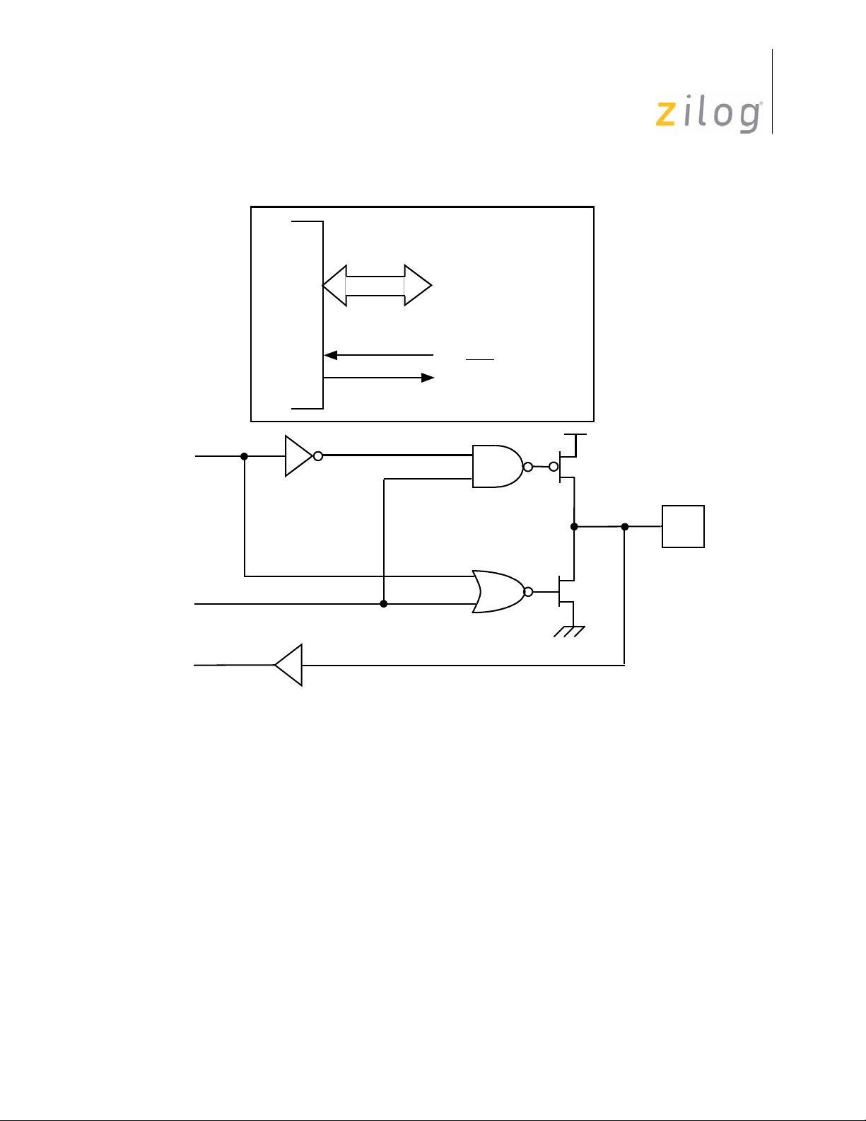
Z8® CPU
User Manual
50
OEN
OUT
IN
Z8
TTL Level Shifter
8
Port 1
(I/O or AD7–AD0)
Handshake Controls
DAV1
and RDY1
(P33 and P34)
PIN
Figure 35. Port 1 Configuration with TTL Level Shifter
Read/Write Operations
In byte input or byte output mode, the port is accessed as General-Purpose Register P1
(
01h). The port is written by specifying P1 as an instruction's destination register. Writing
to the port causes data to be stored in the port's output register.
The port is read by specifying P1 as the source register of an instruction. When an output
is read, data on the external pins is returned. Under normal loading conditions, this is
equivalent to reading the output register. However, if Port 1 outputs are defined as opendrain, the data returned is the value forced on the output by the external system. This may
not be the same as the data in the output register. When Port 1 is defined as an input, reading also returns data on the external pins. However, inputs under handshake control return
data latched into the input register via the input strobe.
UM001604-0108 Input/Output Ports
Page 58

Z8® CPU
User Manual
Using the Port 0–1 Mode Register, Port 1 is configured as an output port by setting bits D4
and D3 to 0, or as an input port by setting D4 to 0 and D3 to 1 (see Figure 36).
R248 P01M
Port 0–1 Mode Register
(F8, Write-Only)
D4 D3
P10–P13 Mode
00 = Byte Output
01 = Byte Output
10 = AD0-AD7
11 = High Impedance AD0–AD7,
, DS, R/W,
AS
A8–A11, A12–A15
51
Figure 36. Port 1 I/O Operation
Handshake Operations
When used as an I/O port, Port 1 can be placed under handshake control by programming
the Port 3 Mode register bits D4 and D3 both to 1. In this configuration, handshake control
lines are DAV1 (P33) and RDY1 (P34) when Port 1 is an input port, or RDY1 (P33) and
DAV1 (P34) when Port 1 is an output port. See Figure 37 through Figure 39 on page 53.
Handshake direction is determined by the configuration (input and output) assigned to
Port 1. For example, if Port 1 is an output port then handshake is defined as output.
R247 P3M
Port 3 Mode Register
(F7, Write-Only)
D4 D3
Figure 37. Handshake Operation
00 P33 = Input P34 = Output
01 P33 = Input P34 = DM
10 P33 = Input P34 = DM
11 P33 = DAV1
/RDY1 P34 = RDY1/DAV1
UM001604-0108 Input/Output Ports
Page 59

Port 2
Z8® CPU
User Manual
Port 2 is a general-purpose port. Figure 29 on page 45 displays a block diagram of Port 2.
Each of its lines can be independently programmed as input or output via the Port 2 Mode
Register (
F6h) as seen in Figure 38. A bit set to a 1 in P2M configures the corresponding
bit in Port 2 as an input, while a bit set to 0 configures an output line.
Register F6h
Port 2 Mode Register (P2M)
(Write-Only)
D7 D6 D5 D4 D3 D2 D1 D0
Port 2 Mode
0 = Output
1 = Input
52
General Port I/O
Port 2 can be an 8-bit, bidirectional, CMOS- or TTL- compatible I/O port. These eight I/O
lines can be configured under software control to be an input or output, independently.
Input buffers can be Schmitt-Triggered, level-shifted, or a single trip point buffer and may
contain autolatches. Bits programmed as outputs may be globally programmed as either
push-pull or open-drain. Low-EMI output buffers can be globally programmed by the software, an OTP program option, or as a ROM mask option. In addition, when the SPI is featured and enabled, P20 functions as data-in (DI), and P27 functions as data-out (DO).
Refer to specific product specifications for exact input/output buffer type features available. See Figure 39 on page 53 through Figure 41 on page 54.
Figure 38. Port 2 I/O Mode Configuration
UM001604-0108 Input/Output Ports
Page 60

OPEN-DRAIN
P21–P26 OE
P21–P26 OUT
Z8® CPU
User Manual
53
P21–P26
PIN
P21–P26 IN
1.5
2.3 V Hysteresis @ V
R ≈ 500 K
= 5.0 V
CC
Autolatch
Ω
Figure 39. Port 2 Configuration with Open-Drain Capability, Autolatch, and
Schmitt-Trigger
Open-Drain
OEN
OUT
TTL Level Shifter
PIN
IN
Figure 40. Port 2 Configuration with TTL Level Shifter
UM001604-0108 Input/Output Ports
Page 61

OPEN-DRAIN
P20 OE
SPI EN
P20 OUT
P20 IN
or
SPI DI
OPEN-DRAIN
R ≈ 500 K
Z8® CPU
User Manual
54
P20
PIN
Autolatch
Ω
P27 OUT
SPI DO
P27 OE
SPI Active
P27 IN
Standard
SPI
Standard
SPI
SCON
D2
0 SOI D0 Enable
1 P27 OUT
*SPI must be enabled with D0
R ≈ 500 K
Ω
P27
PIN
Autolatch
Figure 41. Port 2 Configuration with Open-Drain Capability, Autolatch, Schmitt-
Trigger and SPI
Read/Write Operations
Port 2 is accessed as General-Purpose Register P2 (02h). Port 2 is written by specifying
P2 as an instruction’s destination register. Writing to Port 2 causes data to be stored in the
output register of Port 2, and reflected externally on any bit configured as an output.
Port 2 is read by specifying P2 as the source register of an instruction. When an output bit
is read, data on the external pin is returned. Under normal loading conditions, this is
equivalent to reading the output register. However, if a bit of Port 2 is defined as an
UM001604-0108 Input/Output Ports
Page 62
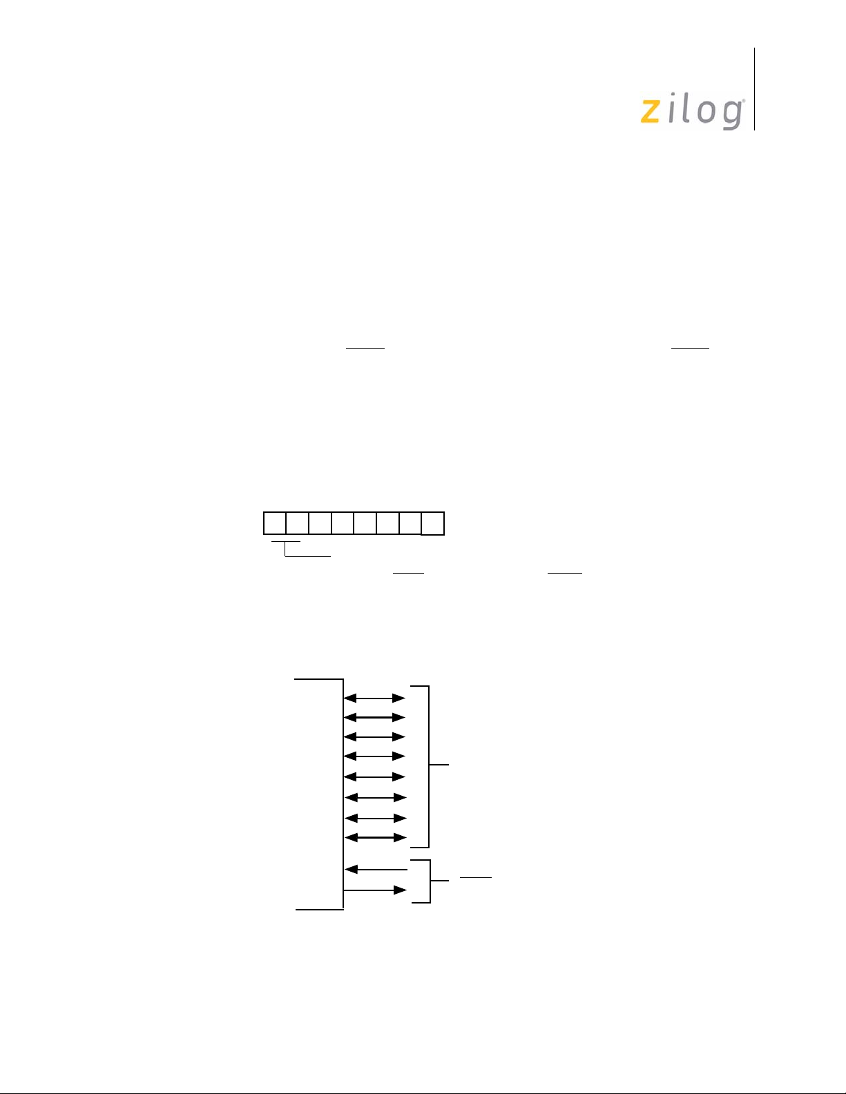
open-drain output, the data returned is the value forced on the output pin by the external
system. This may not be the same as the data in the output register. Reading input bits of
Port 2 also returns data on the external pins. However, inputs under handshake control
return data latched into the input register via the input strobe.
Handshake Operation
Port 2 can be placed under handshake control by programming bit 6 in the Port 3 Mode
Register (see Figure 42). In this configuration, Port 3 lines P31 and P36 are used as the
handshake control lines DAV2
output handshake.
Handshake direction is determined by the configuration (input or output) assigned to bit 7
of Port 2. Only those bits with the same configuration as P27 are under handshake control.
Figure 43 displays the bit lines of Port 2 and the associated handshake lines of Port 3.
Z8® CPU
User Manual
55
and RDY2 for input handshake, or RDY2 and DAV2 for
Register F7h
Port 3 Mode Register
(Write-Only)
D7 D6 D5 D4 D3 D2 D1 D0
Port 2 Handshaking
0 P31 = Input (TIN) P36 = Output (T
1 P31 = DAV2
/RDY2 P36 = RDY2/DAV2
Figure 42. Port 2 Handshake Configuration
P20
Port 2 (I/O)
P27
Handshake Controls
and RDY2
DAV2
(P31 and P36)
OUT
)
Figure 43. Port 2 Handshaking
UM001604-0108 Input/Output Ports
Page 63

Port 3
General Port I/O
Port 3 differs structurally from Ports 0, 1, and 2. Port 3 lines are fixed as four inputs (P33–
P30) and four outputs (P37–P34) Port 3 does not have an input and output register for each
bit. Instead, all of the input lines have one input register, and all of the output lines have an
output register. Port 3 can be a CMOS- or TTL- compatible I/O port. Under software control, the lines can be configured as special control lines for handshake, comparator inputs,
SPI control, external memory status, or I/O lines for the on-board serial and timer facilities. Figure 44 on page 57 displays the block diagram of Port 3.
Z8® CPU
User Manual
56
The inputs can be Schmitt-Triggered, level-shifted, or single-trip point buffered. In some
cases, the Z8
EMI capabilities on the outputs. Refer to specific product specifications for exact input/
output buffer type features. Refer to the sections on counter/timers, Stop Mode Recovery,
serial I/O, comparators, and interrupts for more information on the relationships of Port 3
to that feature.
®
MCU may have autolatches hardwired on certain Port 3 inputs and Low-
UM001604-0108 Input/Output Ports
Page 64

Z8® CPU
User Manual
57
Read
Port
Input
4
Read
4
Port
4
Input
Register
Output
Data
Return
Buffer
4
To Interrupt Timer,
Handshake Logic,
or Serial I/O
Input
Buffer
Buffer
Port
Input
4
Lines
–P3
P3
0
3
Write
Port
4
Internal
Bus
Output
Output
Output
Register
Register
Register
4
From Timer,
Handshake Logic,
or Serial I/O
Figure 44. Port 3 Block Diagram
Output
Output
Buffer
Buffer
Port
Output
4
Lines
–P3
P3
4
7
UM001604-0108 Input/Output Ports
Page 65

Z8® CPU
User Manual
58
P30
P31
P32
P33
Z8
P34
P35
P36
P37
Port 3
(I/O or Control)
Autolatch
P30
P31 (AN1)
P32 (AN2)
P33 (REF)
From Stop-Mode
Recovery Source
R247 = P3M
D1
DIG.
+
-
+
-
AN.
R ≈ 500 K
Ω
1 = Analog
0 = Digital
P30 Data
Latch IRQ3
IRQ2, TIN, P31 Data Latch
IRQ0, P32 Data Latch
IRQ1, P33 Data Latch
Figure 45. Port 3 Configuration with Comparator, Autolatch, and Schmitt-Trigger
UM001604-0108 Input/Output Ports
Page 66

Z8® CPU
User Manual
59
P37 OUT
P32
P37 OUT
P32
PCON
D0
REF (P33)
REF (P33)
+
-
+
-
0 P34, P37 Standard Output
1 P34, P37 Comparator Output
P34
PIN
P37
PIN
Figure 46. Port 3 Configuration with Comparator
UM001604-0108 Input/Output Ports
Page 67

SK IN
SPI EN
SPI MSTR
Z8® CPU
User Manual
60
P34
PIN
SPI EN
P34 OUT
P31
P34 OUT
P31
PCON
D0
REF
REF
+
-
+
-
SK OUT
SS
SPI EN
SPI MSTR
0 P34, P35 Standard Output
1 P34, P35 Comparator Output
MUX
Figure 47. Port 3 Configuration with SPI and Comparator Outputs
P35
PIN
UM001604-0108 Input/Output Ports
Page 68

Port 3 Output Configuration
Z8® CPU
User Manual
61
OUT
TTL Level Shifter
IN
Figure 48.
Port 3 Configuration with TTL Level Shifter and Autolatch
Read/Write Operations
Port 3 is accessed as a General-Purpose Register P3 (03h). Port 3 is written by specifying
P3 as an instruction’s destination register. However, Port 3 outputs cannot be written to if
they are used for special functions. When writing to Port 3, data is stored in the output register.
Port 3 Input Configuration
R ≈ 500 K
Ω
PIN
PIN
Autolatch
Port 3 is read by specifying P3 as the source register of an instruction. When reading from
Port 3, the data returned is both the data on the input pins and in the output register.
Special Functions
Special functions for Port 3 are defined by programming the Port 3 Mode Register. By
writing 0s in bit 6 through bit 1, lines P37–P30 are configured as input/output pairs (see
Figure 49 on page 62). Tabl e 1 7 on page 62 lists available functions for Port 3. The special
functions indicated in the figure are discussed in detail in their corresponding sections in
this manual.
Port 3 input lines P33–P30 always function as interrupt requests regardless of the configuration specified in the Port 3 Mode Register.
UM001604-0108 Input/Output Ports
Page 69

Register F7h
Port 3 Mode Register
(Write-Only)
D7 D6 D5 D4 D3 D2 D1 D0
0 Port 2 Open-Drain
1 Port 2 Push–Pull
0 P31, P32 Digital Mode
1 P31, P32 Analog Mode
0 P32 = Input P35 = Output
00 P33 = Input P34 = Output
01 P33 = Input P34 = DM
10 P33 = Input P34 = DM
0 P31 = Input P36 = Output
Z8® CPU
User Manual
62
0 P30 = Input P37 = Output
1 P30 = Serial In P37 = Serial Out
0 Party ON
1 Party OFF
Figure 49. Port 3 Mode Register Configuration
Table 17. Port 3 Line Functions
Function Line Signal
Inputs P30 Input
P31 Input
P32 Input
P33 Input
Outputs P34 Output
P35 Output
P36 Output
P37 Output
Port 0 Handshake Input P32 DAV0
/RDY0
Port 1 Handshake Input P33 DAV1
Port 2 Handshake Input P31 DAV2
/RDY1
/RDY2
UM001604-0108 Input/Output Ports
Page 70

Table 17. Port 3 Line Functions (Continued)
Function Line Signal
Port 0 Handshake Output P35 RDY0/DAV0
Port 1 Handshake Output P34 RDY1/DAV1
Port 2 Handshake Output P36 RDY2/DAV2
Analog Comparator Input P31 AN1
P32 AN2
P33 REF
Analog Comparator Output P34 AN1-OUT
P35 AN2-OUT
P37 AN2-OUT
Z8® CPU
User Manual
63
Interrupt Requests P30 IRQ3
Serial Input (UART) P30 DI
Serial Output (UART) P37 DO
SPI Slave Select P35 SS
SPI Clock P34 SK
Counter/Timer P31 T
External Memory Status P34 DM
Port Handshake
When Ports 0, 1, and 2 are configured for handshake operation, a pair of lines from Port 3
are used for handshake controls. The handshake controls are interlocked to properly time
asynchronous data transfers between Z8
tions as a strobe from the sender to indicate to the receiver that data is available. The second control line (RDY) acknowledges receipt of the sender’s data, and indicates when the
receiver is ready to accept another data transfer.
P31 IRQ2
P32 IRQ0
P33 IRQ1
IN
P36 T
OUT
®
and a peripheral. One control line (DAV) func-
In input mode, data is latched into the Port’s input register by the first DAV
protected from being overwritten if additional pulses occur on the DAV
signal, and is
line. This over-
write protection is maintained until the port data is read. In output mode, data written to
UM001604-0108 Input/Output Ports
Page 71

Z8® CPU
User Manual
the port is not protected and can be overwritten by the Z8 CPU during the handshake
sequence. To avoid losing data, the software must not overwrite the port until the corresponding interrupt request indicates that the external device has latched the data.
The software can always read Port 3 output and input handshake lines, but cannot write to
the output handshake line.
The following is the recommended setup sequence when configuring a Port for handshake
operation for the first time after a reset:
•
Load P01M or P2M to configure the port for input/output
•
Load P3 to set the Output Handshake bit to a logic 1
•
Load P3M to select HANDSHAKE mode for the port
Once a data transfer begins, the configuration of the handshake lines should not be
changed until the handshake is completed.
64
Figure 50 and Figure 51 on page 65 display detailed operation for the handshake
sequence.
DAV
(Input To Z8)
RDY
utput From Z8)
Data on Port
(Input To Z8)
State 1.
State 2.
State 3.
State 4.
State 5.
213
Valid Data
Port 3 output is High, indicating that the I/O device is ready to accept data.
The I/O device puts data on the port and then activates the DAV
.
into the port input register and generates an interrupt request.
®
The Z8
CPU forces the Ready (RDY) output Low, signaling to the I/O device that the data has been latched.
The I/O device returns the DAV
CPU RR software must respond to the interrupt request and read the contents of the port in order for the
The Z8
handshake sequence to be completed. The RDY line goes High if and only if the port has been read and
DAV
is High. This returns the interface to its initial state.
line High in response to RDY going Low.
input. This causes the data to be latched
45
Figure 50. Z8 Input Handshake
UM001604-0108 Input/Output Ports
Page 72

Z8® CPU
e
User Manual
65
RDY
(Input To Z8)
DAV
(Output From Z8)
Data on Port
(Output From Z8)
State 1.
State 2.
State 3.
State 4.
State 5.
213
Valid Data
RDY input is High indicating that the I/O device is ready to accept data.
®
CPU Writes to the port register to initiate a data transfer. Writing to the port outputs new data and
the Z8
forces DAV
The I/O device forces RDY Low after latching the data. RDY Low causes an interrupt request to be generat
the Z8 CPU can write new data responses to RDY going Low; however, the data is not output until State 5.
The DAV
The DAV
Low if and only if RDY is High.
output from the Z8 CPU is driven High in response to RDY going Low.
goes High, the I/O device is free to raise RDY High thus returning the interface to its initial state.
45
Figure 51. Z8 Output Handshake
In applications requiring a strobed signal instead of the interlocked handshake, Z8® CPU
can satisfy this requirement as follows:
•
In the Strobed Input mode, data can be latched in the Port input register using the DAV
input. The data transfer rate must allow enough time for the software to read the Port
before strobing in the next character. The RDY output is ignored.
•
In the Strobed Output Mode, the RDY input should be tied to the DAV output.
Figure 52 on page 66 and Figure 53 on page 66 display the strobed handshake connec-
tions.
UM001604-0108 Input/Output Ports
Page 73

P20–P27
Z8® CPU
User Manual
66
Z8
P36
P31
Figure 52. Output Strobed Handshake on Port 2
P20–P27
Z8
P31
Figure 53. Input Strobed Handshake on Port 2
DAV
RDY
DAV
I/O
Device
I/O
Device
I/O Port Reset Conditions
Full Reset
After a hardware reset, WDT reset, or a POR, Port Mode Registers P01M, P2M, and P3M
are set as displayed in Figure 54 on page 67 through Figure 56 on page 68. Port 2 is configured for input operation on all bits and is set for open-drain (see Figure 55 on page 67).
If push-pull outputs are required for Port 2 outputs, remember to configure them using
P3M. Note that a WDT time-out from Stop Mode Recovery does not do a full reset. Certain registers that are not reset after Stop Mode Recovery will not be reset.
For the condition of the Ports after Stop Mode Recovery, refer to the specific device product specifications. In some cases, Z8
register set back to the default condition after reset while others do not.
All special I/O functions of Port 3 are inactive, with P33–P30 set as inputs and P37–P34
set as outputs (see Figure 56 on page 68).
UM001604-0108 Input/Output Ports
®
MCU features the P01M, P2M, and P3M control
Page 74

Z8® CPU
User Manual
67
Note:
Because the types and amounts of I/O vary greatly among the Z8® CPU family devices, it is
recommended to review the selected device's product specifications for the register default
state after reset.
Register F8h
Port 0–1 Mode Register (P01M)
(Write-Only)
0 1 0 0 1 1 0 1
P00–P03 Mode
00 = Output
01 = Input
1X = A8–A11
Stack Selection
0 = External
1 = Internal
P10–P17 Mode
00 = Byte Output
01 = Byte Output
10 = AD0–AD7
11 = High Impedance AD0–AD7,
A8–A15, AS
External Memory Timing
Normal = 0
Extended = 1
, DS, R/W
P04–P07 Mode
Output = 00
Input = 01
A12–A15 = 1X
Figure 54. Port 0/1 Reset
Register F6h
Port 2 Mode Register (P2M)
(Write-Only)
1 1 1 1 1 1 1 1
Port 2 Mode
0 = Output
1 = Input
Figure 55. Port 2 Reset
UM001604-0108 Input/Output Ports
Page 75

Register F7h
Port 3 Mode Register (P3M)
(Write-Only)
0 0 0 0 0 0 0 0
0 Port 2 Open-Drain
1 Port 2 Push–Pull
0 P31, P32 Digital Mode
1 P31, P32 Analog Mode
0 P32 = Input P35 = Output
1 P32 = DAV0
00 P33 = Input P34 = Output
01 P33 = Input P34 = DM
10 P33 = Input P34 = DM
11 P33 = DAV1
0 P31 = Input P36 = Output
1 P32 = DAV2/RDY2 P36 = RDY2/DAV2
/RDY0 P35 = RDY0/DAV0
/RDY1 P34 = RDY1/DAV1
Z8® CPU
User Manual
68
Analog Comparators
Select Z8 devices include two independent on-chip analog comparators. See the device
product specification for feature availability and use. Port 3, Pins P31, and P32 each has a
comparator front end. The comparator reference voltage, pin P33, is common to both comparators. In analog mode, the P31, and P32 are the positive inputs to the comparators and
P33 is the reference voltage supplied to both comparators. In digital mode, pin P33 can be
used as a P33 register input or IRQ1 source. P34, P35, or P37 may output the comparator
outputs by software-programming the PCON Register bit D0 to 1.
Comparator Description
Two on-board comparators process analog signals on P31 and P32 with reference to the
voltage on P33. The analog function is enabled by programming the Port 3 Mode Register
(P3M bit 1). For interrupt functions during analog mode, P31 and P32 are programmable
as rising, falling, or both edge triggered interrupts (IRQ register bits 6 and 7).
0 P30 = Input P37 = Output
1 P30 = Serial In P37 = Serial Out
0 Parity OFF
1 Parity ON
Figure 56. Port 3 Mode Reset
Note:
P33 cannot generate an external interrupt while in this mode. P33 can only generate interrupts in DIGITAL mode.
UM001604-0108 Input/Output Ports
Page 76

Z8® CPU
User Manual
Port 3 inputs must be in digital mode if Port 3 is a Stop Mode Recovery source. The analog
comparator is disabled in STOP mode.
69
P31 can be used as T
in analog or digital modes, but it must be referenced to P33, when
IN
in analog mode.
Register F7h
Port 3 Mode Register (P3M)
(Write-Only)
D1
Figure 57. Port 3 Input Analog Selection
ERF Bank F
Register 00h
Port Configuration Register (PCON)
(Write-Only)
D0
Figure 58. Port 3 Comparator Output Selection
0 = Digital Mode P31, P32, P33
1 = Analog Mode P31, P32, P33
0 = P34, P35, or P37 Standard Outputs
1 = P34, P35, or P37 Comparator Outputs
UM001604-0108 Input/Output Ports
Page 77
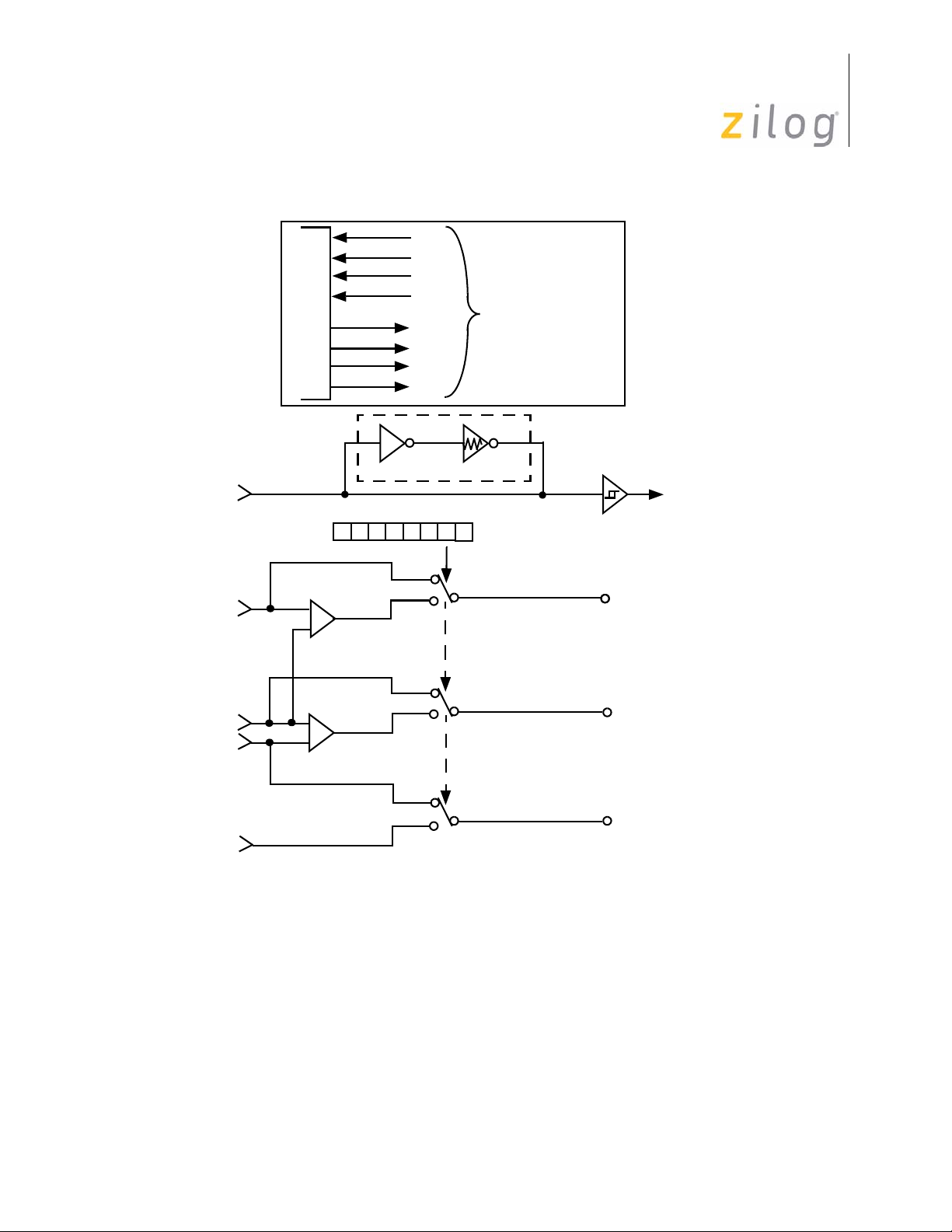
P30
Z8
R247 = P3M
D1
P30
P31
P32
P33
P34
P35
P36
P37
Port 3
(I/O or Control)
R ≈ 500 K
1 = Analog
0 = Digital
Ω
Autolatch
P30 Data
Latch IRQ3
Z8® CPU
User Manual
70
DIG.
P31 (AN1)
P32 (AN2)
P33 (REF)
From Stop-Mode
Recovery Source
+
-
+
-
AN.
IRQ2, TIN, P31 Data Latch
IRQ0, P32 Data Latch
IRQ1, P33 Data Latch
Figure 59. Port Configuration of Comparator Inputs on P31, P32, and P33
UM001604-0108 Input/Output Ports
Page 78

Z8® CPU
User Manual
71
P34 OUT
P31
P37 OUT
P32
PCON
D0
REF (P33)
REF (P33)
+
-
+
-
0 P34, P37 Standard Output
1 P34, P37 Comparator Output
Figure 60. Port 3 Configuration
P34
PIN
P37
PIN
Comparator Programming
Example of enabling analog comparator mode.
LD P3M, #XXXX XX1Xb
X = any binary number
Example of enabling analog comparator output.
LD RP, #%0Fh ;Sets register
pointer to
;working register
group 0
;and Expanded
Register
;File Bank F.
UM001604-0108 Input/Output Ports
Page 79

LD R0, #XXXX XXX1b ;Enables comparator
Comparator Operation
After enabling the Analog Comparator mode, P33 becomes a common reference input for
both comparators. The P33 (Ref) is hard wired to the reference inputs to both comparators
and cannot be separated. P31 and P32 are always connected to the positive inputs to the
comparators. P31 is the positive input to comparator AN1 while P32 is the positive input
to comparator AN2. The outputs to comparators AN1 and AN2 are AN1-out and AN2-out,
respectively.
The comparator output reflects the relationship between the positive input and the reference input.
Z8® CPU
User Manual
72
;outputs using PCON
;Register programming
Example
If the voltage on AN1 is higher than the voltage on Ref then AN1-out is at a high state. If
voltage on AN2 is lower than the voltage on Ref then AN2-out is at a Low state. In this
example, when the Port 3 register is read, Bits D1 = 1 and D2 = 0. If the comparator outputs are enabled to come out on P34 and P37, then P34 = 1 and P37 = 0.
Note:
The previous data stored in P34 and P37 is not disturbed. Once the comparator outputs are
de-selected the stored values in the P34 and P37 register bits are reflected on these pins
again.
Interrupts
P32 (AN2) will generate an interrupt based on the result of the comparison being low and
the Interrupt Request Register (
and D6 = 0 then both P31 and P32 would generate interrupts.
Comparator Definitions
V
ICR
The usable voltage range for both positive inputs and the reference input is called the common mode voltage range (V
are outside of the V
V
OFFSET
The absolute value of the voltage between the positive input and the reference input
required to make the comparator output voltage switch is the input offset voltage (V
). If AN1 is 3.000 V and Ref is 3.001 V when the comparator output switches states
SET
then the V
offset
ICR
= 1 mV.
ICR
range.
IRQ FAh) having bits D7 = 0 and D6 = 0. If IRQ D7 = 1
). The comparator is not guaranteed to work if the inputs
OFF-
UM001604-0108 Input/Output Ports
Page 80

I
IO
For CMOS voltage comparator inputs, the input offset current (IIO) is the leakage current
of the CMOS input gate.
Run Mode
P33 is not available as an interrupt input during analog mode. P31 and P32 are valid interrupt inputs in conjunction with P33 (Ref) when in analog mode.
Z8® CPU
User Manual
73
P31 can still be used as T
when analog mode is selected. If comparator outputs are
IN
required to be outputted on the Port 3 outputs, refer to specific product specification for
priority of mixing when other special features are sharing those same Port 3 pins.
Halt Mode
The analog comparators are functional during HALT mode if analog mode is enabled. P31
and P32, in conjunction with P33 (Ref) are able to generate interrupts. Only P33 cannot
generate an interrupt because the P33 input goes directly to the Ref input of the comparators and is disconnected from the interrupt sensing circuits.
Stop Mode
The analog comparators are disabled during STOP mode so it does not use any current at
that time. If P31, P32, or P33 are used as a source for Stop Mode Recovery, the Port 3 digital mode must be selected by setting bit D1 = 0 in the Port 3 Mode Register. Otherwise in
STOP mode, the P31, P32, and P33 cannot be sensed. If analog mode is selected when
entering STOP mode, it is still enabled after a valid SMR triggered reset.
Open-Drain Configuration
All Z8® MCUs can configure Port 2 to provide open-drain outputs by programming the
Port 3 Mode Register (P3M) bit D0 = 0.
Register F7h
Port 3 Mode Register
(Write-Only)
D7 D6 D5 D4 D3 D2 D1 D0
Figure 61. Port 2 Configuration
UM001604-0108 Input/Output Ports
Port 2 Configuration
1 = Pull-Ups Open-Drain
0 = Pull-Ups Active
Page 81

Z8® CPU
User Manual
Other Z8 MCUs feature a Port Configuration Register (PCON) for which Port 0 and Port 1
can be configured to provide open-drain outputs. The PCON Register is located in ERF
Bank F, Register
PCON (Fh) 00h
D7 D6 D5 D4 D3 D2 D1 D0
00h. See Figure 62 on page 74.
* Default Setting After RESET
Comparator Output Port 3
0 P34, P37 Standard Output*
1 P34, P37 Comparator Output
0 Port 1 Open Drain
1 Port 1 Push–pull Active *
0 Port 0 Open Drain
1 Port 0 Push–pull Active *
0 Port 0 Low EMI
1 Port 0 Standard *
0 Port 1 Low EMI
1 Port 1 Standard *
0 Port 2 Low EMI
1 Port 2 Standard *
0 Port 3 Low EMI
1 Port 3 Standard *
Low EMI Oscillator
0 Low EMI
1 Standard *
74
Figure 62. Port Configuration Register (Write-Only)
Port 1 Open-Drain—Port 1, D1 can be configured as open-drain by resetting this bit (D1
= 0) or configured as push–pull active by setting this bit (D1 = 1). The default value is 1.
Port 0 Open Drain—Port 0, D2 can be configured as open-drain by resetting this bit (D2
= 0) or configured as push–pull active by setting this bit (D2 = 1). The default value is 1.
Low EMI Emission
Some Z8® MCUs can be programmed to operate in a Low EMI Emission Mode using the
Port configuration register (PCON). The PCON register allows the oscillator and all I/O
ports to be programmed in the Low-EMI Mode independently. Other Z8 MCUs may offer
a ROM Mask or OTP programming option to configure the Z8 MCU ports and oscillator
globally to a Low-EMI mode (where the XTAL frequency is set equal to the internal system clock frequency.
Use of the Low EMI feature results in:
•
The output pre-drivers slew rate reduced to 10 ns (typical)
UM001604-0108 Input/Output Ports
Page 82

Z8® CPU
User Manual
•
Low EMI output drivers have resistance of 200 Ω (typical)
•
Low EMI Oscillator
•
All output drivers are approximately 25 percent of the standard drive
•
Internal SCLK ÷ TCLK = XTAL operation limited to a maximum of 4 MHz–250 ns
cycle time, when Low EMI Oscillator is selected and system clock (SCLK = XTAL,
SMR Reg. Bit D1 = 1)
®
For Z8
options.
Low EMI Port 0—Port 0, D3 can be configured as a Low EMI Port by resetting this bit
(D3 = 0) or configured as a Standard Port by setting this bit (D3 = 1). The default value
is 1.
Low EMI Port 1—Port 1, D4 can be configured as a Low EMI Port by resetting this bit
(D4 = 0) or configured as a Standard Port by setting this bit (D4 = 1). The default value
is 1.
MCUs having the PCON register feature, the following bits control the Low EMI
75
Low EMI Port 2—Port 2, D5 can be configured as a Low EMI Port by resetting this bit
(D5 = 0) or configured as a Standard Port by setting this bit (D5 = 1). The default value
is 1.
Low EMI Port 3—Port 3, D6 can be configured as a Low EMI Port by resetting this bit
(D6 = 0) or configured as a Standard Port by setting this bit (D6 = 1). The default value
is 1.
Low EMI OSC—This D7 bit of the PCON Register controls the Low EMI oscillator. A 1
in this location configures the oscillator with standard drive, while a 0 configures the
oscillator with low noise drive. The Low-EMI mode reduces the drive of the oscillator
(OSC). The default value is 1. XTAL ÷ 2 mode is not affected by this bit.
Note:
The maximum external clock frequency is 4 MHz when running in the Low EMI oscillator
mode.
Refer to the selected device product specification for availability of the Low EMI feature
and programming options.
Input Protection
All CMOS ROM Z8 MCUs have I/O pins with diode input protection. There is a diode
from the I/O pad to V
and to VSS. See Figure 63 on page 76.
CC
UM001604-0108 Input/Output Ports
Page 83

PIN
Z8® CPU
User Manual
76
V
CC
V
SS
Figure 63. Diode Input Protection
On CMOS OTP EPROM Z8® MCUs, the Port 3 inputs P31, P32, P33, and the XTAL 1
pin have only the input protection diode from pad to V
PIN
V
SS
Figure 64. OTP Diode Input Protection
. See Figure 64.
SS
The high-side input protection diodes were removed on these pins to allow the application
of +12.5 V during the various OTP programming modes.
For better noise immunity in applications that are exposed to system EMI, a clamping
diode to V
from these pins may be required to prevent entering the OTP programming
CC
mode or to prevent high voltage from damaging these pins.
UM001604-0108 Input/Output Ports
Page 84

Z8® CMOS Autolatches
I/O port bits that are configurable as inputs are protected against open circuit conditions
using autolatches. An autolatch is a circuit which, in the event of an open circuit condition,
latches the input at a valid CMOS level. This inhibits the tendency of the input transistors
to self-bias in the forward active region, thus drawing excessive supply current. A simplified schematic of the CMOS Z8 I/O circuit is displayed in Figure 65.
V
DD
P
Z8® CPU
User Manual
77
Open-Drain
OE
Data Out
PIN
N
V
DD
Autolatch
P
N
Figure 65. Simplified CMOS Z8 I/O Circuit
Data In
G1
The operation of the autolatch circuit is straight-forward. Assume the input pad is latched
at +5V (logic 1). The inverter G1 inverts the bit, turning the P-channel FET ON and the Nchannel FET OFF. The output of the circuit is effectively shorted to V
, returning +5V to
DD
the input. If the pad is then disconnected from the +5V source, the autolatch hold the input
at the previous state. If the device is powered up with the input floating, the state of the
autolatch is at either supply, but which state is unpredictable.
There are four operating conditions which activate the autolatches. The first, which occurs
when the input pin is physically disconnected from any source, is the most obvious. The
UM001604-0108 Input/Output Ports
Page 85

second occurs when the input is connected to the output of a device with tri-state capability.
The autolatch also activates when the input voltage at the pin is not within 200 microvolts
or so of either supply rail. In this case, the circuit draws current, which is not significant
compared to the I
rent of the device dramatically.
The fourth condition occurs when the I/O bit is configured as an output. As displayed in
Figure 65 on page 77, there are two ways of tri-stating the port pin. The first is by config-
uring the port as an input, which disables the OE
second can be achieved in output mode by writing a 1 to the output port, then activating
the open-drain mode. Both transistors are again OFF, and the port bit is in a high impedance state. The autolatches then pull the input section toward V
Autolatch Model
operating current of the device, but increases I
CC
signal turning both transistors OFF. The
DD
User Manual
STOP mode cur-
CC2
.
Z8® CPU
78
The autolatch’s equivalent circuit is displayed in Figure 66. When the input is high, the
circuit consists of a resistance Rp from V
a much greater resistance Rh to G
. Current IAO flows from VDD to the output. When
ND
the input is low, the circuit may be modeled as a resistance Rp from G
transistor in the ON state) and a much greater resistance Rh to V
flows from the input to ground. The autolatch is characterized with respect to I
equivalent resistance Rp is calculated according to R
equivalent resistance Rp (min) may be calculated at the worst case input voltage, V
(the P-channel transistor in its ON state) and
DD
(the N-channel
ND
. Current IAO now
DD
, so the
AO
= (VDD–VIN)/IAO. The worst case
P
= V
I
(min).
A0
VDD
R
RP
H
Data in
Logic 0
PIN
VDD
A0
RP
Data in
Logic 1
R
H
Figure 66. Autolatch Equivalent Circuit
PIN
IH
Design Considerations
For circuits in which the autolatch is active, considerations should be given to the loading
constraints of the autolatches. For example, with weak values of V
UM001604-0108 Input/Output Ports
, close to Vih (min) or
IN
Page 86

Z8® CPU
User Manual
Vil (max), pullup or pull-down resistances must be calculated using Ref = R/Rp. For best
case STOP mode operation, the inputs should be within 200 mV of the supply rails.
In output mode, if a port bit is forced into a tri-state condition, the autolatches force the
pad to V
. If there is an external pulldown resistor on the pin, the voltage at the pin may
DD
not switch to GND due to the autolatch. As displayed in Figure 67, the equivalent resistance of the autolatch and the external pulldown forms a voltage divider, and if the external resistor is large, the voltage developed across it will exceed V
VIL(max > VDD [R
R
(max) = [(VIL(max) ÷ VDD) RP] ÷ [1—(VIL(max) ÷ VDD)]
EXT
For V
R
= 5.0 V and IAO = 5 µA, VIH(max) = 0.8 V:
DD
(max) = (0.16 ÷ 1M) ÷ (1—0.16) = 190 K¾.
EXT
EXT
÷ (R
EXT
+ RP)]
(max). For worst case.
IL
Rp increases rapidly with VDD, so increased VDD will relax the requirement on Rext.
In summary, the CMOS Z8 autolatch inhibits excessive current drain in Z8 devices by
latching an open input to either V
acteristics of the device may be modeled by a current I
V
DD/IAO
.
or GND. The effect of the autolatch on the I/O char-
DD
and a resistor Rp, whose value is
AO
79
V
LO
RP
VIH (min.)
R
EXT
Figure 67. Effect of Pulldown Resistors on Autolatches
UM001604-0108 Input/Output Ports
Page 87

Counters and Timers
Z8® CPU provides up to two 8-bit counter/timers, T0 and T1, each driven by its own 6-bit
prescaler, PRE0 and PRE1 (see Figure 68). Both counter/timers are independent of the
processor instruction sequence, that relieves software from time-critical operations such as
interval timing or event counting. Some MCUs offer clock scaling using the SMR. Refer
to the device product specification for clock available options.
Each counter/timer operates in either Single-Pass or Continuous mode. At the end-ofcount, counting either stops or the initial value is reloaded and counting continues. Under
software control, new values are loaded immediately or when the end-of-count is reached.
Software also controls the counting mode, how a counter/timer is started or stopped, and
its use of I/O lines. Both the counter and prescaler registers can be altered while the
counter/timer is running.
Z8® CPU
User Manual
80
D1 (SMR)
D0 (SMR)
OSC
÷2
÷16
Clock
Logic
TIN P31
Internal
Clock
External Clock
÷4
Internal Clock
Gated Clock
Triggered Clock
Internal Data Bus
Write
T0
Initial Value
Register
8-Bit
Down
Counter
8-Bit
Down
Counter
T1
Initial Value
Register
Write
Internal Data Bus
÷4
Write
Write
PRE0
Initial Value
Register
6-Bit
Down
Counter
6-Bit
Down
Counter
PRE1
Initial Value
Register
Figure 68. Counter/Timer Block Diagram
Read
T0
Current Value
Register
T1
Current Value
Register
Read
÷2
IRQ
IRQ
T
OUT
P36
5
4
Counter/timers 0 and 1 are driven by a timer clock generated by dividing the internal clock
by four. The divide-by-four stage, the 6-bit prescaler, and the 8-bit counter/timer form a
synchronous 16-bit divide chain. Counter/timer 1 can also be driven by an external input
UM001604-0108 Counters and Timers
Page 88

Z8® CPU
User Manual
81
(TIN) using P31. Port 3 line P36 can serve as a timer output (T
or the internal clock can be output. The timer output toggles at the end-of-count.
The counter/timer, prescaler, and associated mode registers are mapped into the register
file as displayed in Figure 69. This allows the software to treat the counter/timers as general-purpose registers, and eliminates the requirement for special instructions.
Prescalers and Counter/Timers
The prescalers, PRE0 (F5h) and PRE1 (F3h), each consists of an 8-bit register and a 6bit down-counter as displayed in Figure 68 on page 80. The prescaler registers are writeonly registers. Reading the prescalers returns the value
Figure 71 on page 82 displays the prescaler registers.
The six most significant bits (D2–D7) of PRE0 or PRE1 hold the prescalers count modulo,
a value from 1 to 64 decimal. The prescaler registers also contain control bits that specify
T0 and T1 counting modes. These bits also indicate whether the clock source for T
internal or external. These control bits will be discussed in detail throughout this chapter.
The counter/timer registers, T0 (
counter, a write-only register that holds the initial count value, and a read-only register
that holds the current count value (see Figure 68 on page 80). The initial value can range
from 1 to 256 decimal (
01h,02h,..,00h). Figure 72 on page 83 displays the counter/timer
registers.
F4h) and T1 (F2h), each consists of an 8-bit down-
) through which T0, T1,
OUT
FFh. Figure 70 on page 82 and
is
1
DEC
247
245
244
243
242
241
Figure 69. Counter/Timer Register Map
Port 3 Mode
T0 Prescaler
Timer/Counter0
T1 Prescaler
Time/Counter1
Timer Mode
HEX Identifiers
F7
F5
F4
F3
F2
F1
UM001604-0108 Counters and Timers
Page 89

R245 PRE0
Prescaler 0 Register
(%F5; Write-Only)
D7 D6 D5 D4 D3 D2 D1 D0
Figure 70. Prescaler 0 Register
Count Mode
Single Pass
0 = T
0
1 = T0 Modulo-n
Reserved (Must be 0)
Prescaler Modulo
(Range: 1-64 Decimal
01-00 HEX)
Z8® CPU
User Manual
82
R243 PRE1
Prescaler 1 Register
(%F3; Write-Only)
U U U U U U 0 0
Figure 71. Prescaler 1 Register
Count Mode
Single Pass
0 = T
1
1 = T1 Modulo-n
Clock Source
1 = T1 Internal
0 = T1 External (TIN)
Prescaler Modulo
(Range: 1-64 Decimal
01-00 HEX)
UM001604-0108 Counters and Timers
Page 90

R242 T1
Counter/Timer 1 Register
(%F2; Write/Read Only)
R244 T0
Counter/Timer 0 Register
(%F4; Write/Read Only)
D7 D6 D5 D4 D3 D2 D1 D0
Initial value when written
(Range 1-256 decimal, 01-00 HEX)
current value when read
Figure 72. Counter/Timer 0 and 1 Registers
Z8® CPU
User Manual
83
Counter/Timer Operation
Under software control, counter/timers are started and stopped via the Timer Mode Register (TMR,
bit and an Enable Count bit.
Load and Enable Count Bits
Setting the Load bit (D0 for T0 and D2 for T1) transfers the initial value in the prescaler
and the counter/timer registers into their respective down-counters. The next internal
clock resets bits D0 and D2 to 0, readying the Load bit for the next load operation. New
values may be loaded into the down-counters at any time. If the counter/timer is running, it
continues to do so and starts the count over with the new value. Therefore, the Load bit
actually functions as a software re-trigger.
F1h) bits D0–D3 (see Figure 73). Each counter/timer is associated with a Load
R241 TMR
Timer Mode Register
(% F1; Read/Write)
D3 D2 D1 D0
Figure 73. Timer Mode Register
0 = No Function
1 = Load T
0 = Disable T0 Count
1 = Enable T
0 = No Function
1 = Load T
0 = Disable T
1 = Enable T
0
1
0
1
1
Count
Count
Count
UM001604-0108 Counters and Timers
Page 91

Z8® CPU
User Manual
The counter timers remain at rest as long as the Enable Count bits are 0. To enable counting, the Enable Count bit (D
for T0 and D3 for T1) must be set to 1. Counting actually
1
starts when the Enable Count bit is written by an instruction. The first decrement occurs
four internal clock periods after the Enable Count bit has been set. If T1 is configured to
use an external clock, the first decrement begins on the next clock period. The Load and
Enable Count bits can be set at the same time. For example, using the instruction:
OR TMR,#03h
sets both D0 and D1 of the TMR. This loads the initial values of PRE0 and T0 into their
respective counters and starts the count after the M2T2 machine state after the operand is
fetched (see Figure 74).
R243 PRE1
Prescaler 1 Register
(% F3; Write-Only)
R245 PRE0
Prescaler 0 Register
(% F5; Write-Only)
D0
84
M3 M1 M2 Mn
T1 T2 T3 T1 T2 T3 T1 T2 T3 T1 T2 T3
Prescaler Operations
During counting, the programmed clock source drives the 6-bit Prescaler Counter. The
counter is counted down from the value specified by bits of the corresponding Prescaler
Register, PRE0 (bit 7 to bit 2) or PRE1 (bit 7 to bit 2; see Figure 70 and Figure 71 on page
Count Mode
0 = T
Single Pass
1
1 = T
Modulo-n
1
Figure 74. Starting The Count
First Decrement Occurs
Four Clock Periods Later
TMR is Written, Counter/Timer
is Loaded
#03h is Fetched
Figure 75. Counting Modes
UM001604-0108 Counters and Timers
Page 92

Z8® CPU
User Manual
82). When the Prescaler Counter reaches its end-of-count, the initial value is reloaded and
counting continues. The prescaler never actually reaches 0. For example, if the prescaler is
set to divide-by-three, the count sequence is:
3–2–1–3–2–1–3–2–1–3...
Each time the prescaler reaches its end of count a carry is generated, that allows the
Counter/Timer to decrement by one on the next timer clock input. When the Counter/
Timer and the prescaler both reach the end-of-count, an interrupt request is generated
(IRQ4 for T0, IRQ5 for T1). Depending on the counting mode selected, the Counter/Timer
either comes to rest with its value at
00h (SINGLE-PASS Mode) or the initial value is
automatically reloaded and counting continues (Continuous Mode). The counting modes
are controlled by bit 0 of PRE0 and bit 0 of PRE1 (see Figure 75 on page 84). A 0, written
to this bit configures the counter for Single-pass counting mode, while a 1 written to this
bit configures the counter for Continuous mode.
85
Note:
The Counter/Timer can be stopped at any time by setting the Enable Count bit to 0, and
restarted by setting it back to 1. The Counter/Timer continues its count value at the time it
was stopped. The current value in the Counter/Timer can be read at any time without
affecting the counting operation.
The prescaler registers are write-only and cannot be read.
New initial values can be written to the prescaler or the Counter/Timer registers at any
time. These values are transferred to their respective down counters on the next load operation. If the Counter/Timer mode is continuous, the next load occurs on the timer clock
following an end-of-count. New initial values should be written before the load operation,
because the prescalers always effectively operate in Continuous count mode.
The time interval (i) until end-of-count, is given by the equation:
i = t x p x v
in which t = four times the internal clock period.
The internal clock frequency defaults to the external clock source (XTAL, ceramic resonator, and others) divided by 2. Some Z8 microcontrollers allow this divisor to be changed
via the Stop Mode Recovery register. See the product data sheet for available clock divisor
options.
t is equal to eight divided-by-XTAL frequency of the external clock source for T1 (external clock mode only).
p = the prescaler value (1–63) for T
The minimum prescaler count of 1 is achieved by loading
caler count of 63 is achieved by loading
and T1.
0
111111xx.
000001xx. The maximum pres-
v = the Counter/Timer value (1–256)
UM001604-0108 Counters and Timers
Page 93

Z8® CPU
User Manual
Minimum duration is achieved by loading 01h (1 prescaler output count), maximum duration is achieved by loading
00h (256 prescaler outputs counts).
The prescaler and counter/timer are true divide-by-n counters.
86
T
OUT
Modes
The Timer Mode Register TMR (F1h; see Figure 76), is used in conjunction with the Port
3 Mode Register P3M (
and T1. In order for T
F7h; see Figure 77) to configure P36 for T
to function, P36 must be defined as an output line by setting
OUT
P3M bit 5 to 0. Output is controlled by one of the counter/timers (T0 or T1) or the internal
clock.
Register F1hR
Timer Mode Register (TMR)
(Read/Write)
D7 D6 D3 D0
0 = No Function
1 = Load T
0 = Disable T1 Count
1 = Enable T
T
OUT
T
OUT
OUT = 01
T
0
T1 OUT = 10
Internal Clock OUT = 11
0
Modes:
OFF = 00
1
Count
operation for T0
OUT
Figure 76. Timer Mode Register (T
Register F7h
Port 3 Mode Register (P3M)
(Write-Only)
D7 D6 D5 D4 D3 D2 D1 D0
0 P31 = Input (TIN) P36 = Output (T
1 P31 = DAV2
/RDY2 P36 = RDY2/DAV2
Figure 77. Port 3 Mode Register (T
Operation)
OUT
Operation)
OUT
OUT
)
The counter/timer to be output is selected by TMR bit 7 and bit 6. T0 is selected to drive
the T
UM001604-0108 Counters and Timers
line by setting bit 7 to 0 and bit 6 to 1. Likewise, T1 is selected by setting bit 7
OUT
Page 94

Z8® CPU
User Manual
87
and bit 6 to 1 and 0, respectively. The counter/timer T
mode is turned off by setting
OUT
TMR bit and bit 6 both to 0, freeing P36 to be a data output line.
is initialized to a logic 1 whenever the TMR Load bit (bit 0 for T0 or bit 1 for T2) is
T
OUT
set to 1. The T
timer driving the T
OR TMR,#43h
•
Configures T0 to drive the T
•
Sets the P36 T
•
Loads the initial PRE0 and T0 levels into their respective counters and starts the
configuration timer load, and Timer Enable Count bits for the counter/
OUT
pin can be set at the same time. For example, using the instruction:
OUT
pin (P36)
OUT
pin to a logic 1 level
OUT
counter after the M2T2 machine state after the operand is fetched
At end-of-count, the interrupt request line (IRQ4 or IRQ5), clocks a toggle flip-flop. The
output of this flip-flop drives the T
timer reaches its end-of-count, T
line, P36. In all cases, when the selected counter/
OUT
toggles to its opposite state (see Figure 78). If, for
OUT
example, the counter/timer is in CONTINUOUS COUNTING Mode, Tout has a 50 percent duty cycle output. This duty cycle can easily be controlled by varying the initial values after each end-of-count.
The internal clock can be selected as output instead of T0 or T1 by setting TMR bit 7 and
bit 6 both to 1. The internal clock (XTAL frequency ÷ 2) is then directly output on P36
(see Figure 79 on page 88).
While programmed as T
®
ever, the Z8
software can examine the P36 current output by reading the port register.
, P36 cannot be modified by a write to port register P3. How-
OUT
IRQ
(T0 End-of-Count)
IRQ
(T1 End-of-Count)
UM001604-0108 Counters and Timers
4
5
Figure 78. T0 and T1 Output Through T
TMR
D7–D6 = 01
TMR
D7–D6 = 10
÷2
P36
OUT
T
OUT
Page 95

Internal
Clock
Z8® CPU
User Manual
88
TIN Modes
The Timer Mode Register TMR (F1h; see Figure 80 on page 89) is used in conjunction
with the Prescaler Register PRE1 (
is used in conjunction with T1 in one of four modes:
T
IN
•
•
•
•
Note:
The T
TMR bits 4-5), bit 1 of PRE1 must be set to 0.
7
6
÷2
P3
6
F3h; see Figure 81 on page 89) to configure P31 as T
OUT
T
OUT
OSC
TMR D
TMR D
Figure 79. Internal Clock Output Through T
External Clock Input
Gated Internal Clock
Triggered Internal Clock
Retriggerable Internal Clock
mode is restricted for use with timer 1 only. To enable the TIN mode selected (via
IN
IN
.
The counter/timer clock source must be configured for external by setting the PRE1 Register bit 2 to 1. The Timer Mode Register bit 5 and bit 4 can then be used to select the
appropriate T
For T1 to start counting as a result of a T
must be set to 1. When using T
operation.
IN
input, the Enable Count bit (bit 3 in TMR)
IN
as an external clock or a gate input, the initial values
IN
must be loaded into the down counters by setting the Load bit (bit 2 in TMR) to a 1 before
counting begins. In the descriptions of T
that follow, it is assumed the programmer has
IN
performed these operations. Initial values are automatically loaded in Trigger and Retrigger modes so software loading is unnecessary.
UM001604-0108 Counters and Timers
Page 96

Register F1h
Timer Mode Register (TMR)
(Read/Write)
D5 D4
T
= Modes:
IN
External Clock Input = 00
Gate Input = 01
Trigger Input = 10
Trigger Input = 11
(Non-retriggerable)
(Retriggerable)
Figure 80. Timer Mode Register (TIN Operation)
Z8® CPU
User Manual
89
Register F3h
Prescaler 1 Register (PRE1)
(Write-Only)
D7 D6 D5 D4 D3 D2 D1 D0
Figure 81. Prescaler 1 Register (T
It is suggested that P31 be configured as an input line by setting P3M Register bit 5 to 0,
although T
is still functional if P31 is configured as a handshake input.
IN
Each High-to-Low transition on T
selected T
mode or the enabled/disabled state of T1. IRQ2 must therefore be masked or
IN
enabled according to the requirements of the application.
External Clock Input Mode
The TIN External Clock Input Mode (TMR bit 5 and bit 4 both set to 0) supports counting
of external events, where an event is considered to be a High-to-Low transition on T
(see Figure 82).
Clock Source
External Enable TIN Mode
0 = T
1
1 = T1 Internal Disable TIN Mode
Operation)
IN
generates an interrupt request IRQ2, regardless of the
IN
IN
Note:
See the product data sheet for the minimum allowed T
T
).
IN
external clock input period (TP
IN
UM001604-0108 Counters and Timers
Page 97

T
IN
Clock
P3
1
Internal
Clock
Figure 82. External Clock Input Mode
Gated Internal Clock Mode
The TIN Gated Internal Clock Mode (TMR bit 5 and bit 4 set to 0 and 1 respectively) measures the duration of an external event. In this mode, the T1 prescaler is driven by the
internal timer clock, gated by a High level on T
High and stops counting while T
High-to-Low transition of T
is generated if T1 reaches its end-of-count.
Z8® CPU
User Manual
TMR
D5–D4 = 00
IRQ
IRQ
5
2
D
D
IN
is Low. Interrupt request IRQ2 is generated on the
IN
signalling the end of the gate input. Interrupt request IRQ5
IN
PRE1
(see Figure 83). T1 counts while TIN is
T1
90
÷
T
IN
Gate
OSC
P3
1
2
D D
TMR
D
5–D4 =
Figure 83. Gated Clock Input Mode
Triggered Input Mode
The TIN Triggered Input Mode (TMR bits 5 and 4 are set to 1 and 0, respectively) causes
T1 to start counting as the result of an external event (see Figure 84 on page 91). T1 is then
loaded and clocked by the internal timer clock following the first High-to-Low transition
on the T
Enable bit is reset whenever T1 reaches its end-of-count. Further T
effect on T1 until software sets the Enable Count bit again. In CONTINUOUS mode, once
input. Subsequent TIN transitions do not affect T1. In SINGLE-PASS mode, the
IN
01
Internal
Clock
÷
4
PRE1
T1
transitions have no
IN
IRQ
IRQ
5
2
UM001604-0108 Counters and Timers
Page 98

Z8® CPU
User Manual
T1 is triggered counting continues until software resets the Enable Count bit. Interrupt
request IRQ5 is generated when T1 reaches its end-of-count.
91
÷
T
IN
Trigger
OSC
P3
1
2
D D
Figure 84. Triggered Clock Mode
Retriggerable Input Mode
The TIN Retriggerable Input Mode (TMR bits 5 and 4 are set to 1) causes T1 to load and
start counting on every occurrence of a High-to-Low transition on T
Interrupt request IRQ5 is generated if the programmed time interval (determined by T1
prescaler and counter/timer register initial values) has elapsed because of the last High-toLow transition on T
bit. Subsequent T
sets the Enable Count bit again. In Continuous Mode, counting continues once T1 is triggered until software resets the Enable Count bit. When enabled, each High-to-Low T
transition causes T1 to reload and restart counting. Interrupt request IRQ5 is generated on
every end-of-count.
. In SINGLE-PASS Mode, the end-of-count resets the Enable Count
IN
transitions do not cause T1 to load and start counting until software
IN
Internal
Clock
Edge
Trigger
TMR
D
5 =
TMR
D
5–D4 =
1
÷
4
PRE1
T1
11
, see Figure 84.
IN
IRQ
IRQ
5
2
IN
Cascading Counter/Timers
For some applications, it may be necessary to measure a time interval greater than a single
counter/timer can measure. In this case, T
and T
IN
as a single unit (see Figure 85 on page 92). T0 should be configured to operate in Continuous mode and to drive T
and wired back to T
OUT
. TIN should be configured as an external clock input to T1
OUT
. On every other T0 end-of-count, T
transition that causes T1 to count.
T1 can operate in either Single-Pass or Continuous mode. When the T1 end-of-count is
reached, interrupt request IRQ5 is generated. Interrupt requests IRQ2 (T
transitions) and IRQ4 (T0 end-of-count) are also generated but are most likely of no
importance in this configuration and should be disabled.
UM001604-0108 Counters and Timers
can be used to cascade T0 and T1
OUT
undergoes a High-to-Low
OUT
High-to-Low
IN
Page 99

Z8® CPU
User Manual
92
OSC
2
÷
4
÷
Reset Conditions
After a hardware reset, the counter/timers are disabled and the contents of the counter/
timer and prescaler registers are undefined. However, the counting modes are configured
for Single-Pass and the T1 clock source is set for external.
R242 T1
Counter/Timer 1 Register
(%F2; Write/Read Only)
R244 T0
Counter/Timer 0 Register
(%F4; Write/Read Only)
U U U U U U U U
PRE0 T0
÷
P3
2PRE1
IRQ
6
T
T
OUT
IN
4
Figure 85. Cascaded Counter/Timers
Initial value when written
(Range 1–256 decimal, 01–00 HEX)
current value when read
P3
IRQ
T1
2
1
IRQ
5
Figure 86. Counter/Timer Reset
T
is set for External Clock mode, and the T
IN
mode is OFF. Figure 87 on page 93
OUT
through Figure 89 on page 94 displays the binary reset values of the Prescaler, Counter/
Timer, and Timer Mode registers.
UM001604-0108 Counters and Timers
Page 100

R243 PRE1
PRESCALER 1 REGISTER
(%F3; W
U U U U U U 0 0
RITE-ONLY)
COUNT MODE
0 = T1 SINGLE PASS
1 = T1 MODULO-N
CLOCK SOURCE
1 = T1 INTERNAL
0 = T1 EXTERNAL (TIN)
P
RESCALER MODULO
(RANGE: 1–64 DECIMAL
01–00 HEX)
Z8® CPU
User Manual
93
Figure 87. Prescaler 1 Register Reset
R245 PRE0
Prescaler 0 Register
(%F5; Write-Only)
U U U U U U U 0
Count Mode
0 = T
1 = T0 Modulo-n
Reserved (Must be 0)
Prescaler Modulo
(Range: 1–64 Decimal
01–00 HEX)
Figure 88. Prescaler 0 Reset
Single Pass
0
UM001604-0108 Counters and Timers
 Loading...