

Page 1

SCC/ESCC
User Manual
UM010903-0515
Copyright © 2015 by Zilog®, Inc. All rights reserved.
ww.zilog.com
w
Page 2

SCC/ESCC
User Manual
ii
Warning:
DO NOT USE IN LIFE SUPPORT
LIFE SUPPORT POLICY
ZILOG'S PRODUCTS ARE NOT AUTHORIZED FOR USE AS CRITICAL COMPONENTS IN LIFE
SUPPORT DEVICES OR SYSTEMS WITHOUT THE EXPRESS PRIOR WRITTEN APPROVAL OF
THE PRESIDENT AND GENERAL COUNSEL OF ZILOG CORPORATION.
As used herein
Life support devices or systems are devices which (a) are intended for surgical implant into the body, or (b)
support or sustain life and whose failure to perform when properly used in accordance with instructions for
use provided in the labeling can be reasonably expected to result in a significant injury to the user. A
critical component is any component in a life support device or system whose failure to perform can be
reasonably expected to cause the failure of the life support device or system or to affect its safety or
effectiveness.
Document Disclaimer
©2015 by Zilog, Inc. All rights reserved. Information in this publication concern
applications, or technology
described is intended to suggest possible uses and may be superseded. ZILOG,
ing the devices,
INC. DOES NOT ASSUME LIABILITY FOR OR PROVIDE A REPRESENTATION OF ACCURACY
OF THE INFORMATION, DEVICES, OR TECHNOLOGY DESCRIBED IN THIS DOCUMENT.
ZILOG ALSO DOES NOT ASSUME LIABILITY FOR INTELLECTUAL PROPERTY
INFRINGEMENT RELATED IN ANY MANNER TO USE OF INFORMATION, DEVICES, OR
TECHNOLOGY DESCRIBED HEREIN OR OTHERWISE. The information contained within this
document has been verified according to the general principles of electrical and mechanical engineering.
Z8, Z80 are registered trademarks of Zilog, Inc. All other product or service names are the property of their
respective owners.
UM010903-0515
Page 3

Revision History
Each instance in Revision History reflects a change to this document from its previous
revision. For more details, refer to the corresponding pages and appropriate links in the
table below.
Revision
Date
May 2015 03 Updated /SYNCA and /SYNCB
June 2009 02 Added Low Voltage ESCC information All
May 2009 01 Original Document All
Level Description Page No
Updated /RTxCA, /RTxCB
Updated Data Encoding Method Figure
SCC/ESCC
User Manual
iii
14
15
75
UM010903-0515
Page 4

Table of Contents
General Description . . . . . . . . . . . . . . . . . . . . . . . . . . . . . . . . . . . . . . . . . . . . . . . . . . 1
Introduction . . . . . . . . . . . . . . . . . . . . . . . . . . . . . . . . . . . . . . . . . . . . . . . . . . . 1
SCC’s Capabilities . . . . . . . . . . . . . . . . . . . . . . . . . . . . . . . . . . . . . . . . . . . . . . 2
Block Diagram . . . . . . . . . . . . . . . . . . . . . . . . . . . . . . . . . . . . . . . . . . . . . . . . . 5
Pin Descriptions . . . . . . . . . . . . . . . . . . . . . . . . . . . . . . . . . . . . . . . . . . . . . . . 7
Pin Descriptions 9
Pins Common to both Z85X30 and Z80X30. . . . . . . . . . . . . . . . . . . . . . . 13
Pin Descriptions, (Z85X30 Only) . . . . . . . . . . . . . . . . . . . . . . . . . . . . . . . 15
Pin Descriptions, (Z80X30 Only) . . . . . . . . . . . . . . . . . . . . . . . . . . . . . . . 16
Interfacing the SCC/ESCC. . . . . . . . . . . . . . . . . . . . . . . . . . . . . . . . . . . . . . . . . . . . 17
Introduction . . . . . . . . . . . . . . . . . . . . . . . . . . . . . . . . . . . . . . . . . . . . . . . . . . 17
Z80X30 Interface Timing . . . . . . . . . . . . . . . . . . . . . . . . . . . . . . . . . . . . . . . . 17
Z80X30 Read Cycle Timing . . . . . . . . . . . . . . . . . . . . . . . . . . . . . . . . . . . 17
Z80X30 Write Cycle Timing . . . . . . . . . . . . . . . . . . . . . . . . . . . . . . . . . . . 18
Z80X30 Interrupt Acknowledge Cycle Timing . . . . . . . . . . . . . . . . . . . . . 19
Z80X30 Register Access . . . . . . . . . . . . . . . . . . . . . . . . . . . . . . . . . . . . . 21
Z80C30 Register Enhancement . . . . . . . . . . . . . . . . . . . . . . . . . . . . . . . 24
Z80230 Register Enhancements . . . . . . . . . . . . . . . . . . . . . . . . . . . . . . . 25
Z80X30 Reset . . . . . . . . . . . . . . . . . . . . . . . . . . . . . . . . . . . . . . . . . . . . . 26
Z85X30 Interface Timing . . . . . . . . . . . . . . . . . . . . . . . . . . . . . . . . . . . . . . . . 27
Z85X30 Read Cycle Timing . . . . . . . . . . . . . . . . . . . . . . . . . . . . . . . . . . . 28
Z85X30 Write Cycle Timing . . . . . . . . . . . . . . . . . . . . . . . . . . . . . . . . . . . 28
Z85X30 Interrupt Acknowledge Cycle Timing . . . . . . . . . . . . . . . . . . . . . 29
Z85X30 Register Access . . . . . . . . . . . . . . . . . . . . . . . . . . . . . . . . . . . . . 30
Z85C30 Register Enhancement . . . . . . . . . . . . . . . . . . . . . . . . . . . . . . . 32
Z85C30/Z85230/L Register Enhancements . . . . . . . . . . . . . . . . . . . . . . 32
Z85X30 Reset . . . . . . . . . . . . . . . . . . . . . . . . . . . . . . . . . . . . . . . . . . . . . 34
Interface Programming . . . . . . . . . . . . . . . . . . . . . . . . . . . . . . . . . . . . . . . . . 35
I/O Programming Introduction . . . . . . . . . . . . . . . . . . . . . . . . . . . . . . . . . 36
Polling . . . . . . . . . . . . . . . . . . . . . . . . . . . . . . . . . . . . . . . . . . . . . . . . . . . 36
Interrupts . . . . . . . . . . . . . . . . . . . . . . . . . . . . . . . . . . . . . . . . . . . . . . . . . 36
Interrupt Control . . . . . . . . . . . . . . . . . . . . . . . . . . . . . . . . . . . . . . . . . . . . 38
Daisy-Chain Resolution . . . . . . . . . . . . . . . . . . . . . . . . . . . . . . . . . . . . . . 41
Interrupt Acknowledge . . . . . . . . . . . . . . . . . . . . . . . . . . . . . . . . . . . . . . . 44
The Receiver Interrupt . . . . . . . . . . . . . . . . . . . . . . . . . . . . . . . . . . . . . . . 45
Transmit Interrupts and Transmit Buffer Empty Bit . . . . . . . . . . . . . . . . . 49
SCC/ESCC
User Manual
iv
UM010903-0515
Page 5

SCC/ESCC
User Manual
External/Status Interrupts . . . . . . . . . . . . . . . . . . . . . . . . . . . . . . . . . . . . 56
Block/DMA Transfer . . . . . . . . . . . . . . . . . . . . . . . . . . . . . . . . . . . . . . . . . . . 60
Block Transfers . . . . . . . . . . . . . . . . . . . . . . . . . . . . . . . . . . . . . . . . . . . . 60
DMA Requests . . . . . . . . . . . . . . . . . . . . . . . . . . . . . . . . . . . . . . . . . . . . 63
Test Functions . . . . . . . . . . . . . . . . . . . . . . . . . . . . . . . . . . . . . . . . . . . . . . . . 69
Local Loopback . . . . . . . . . . . . . . . . . . . . . . . . . . . . . . . . . . . . . . . . . . . . 69
Auto Echo. . . . . . . . . . . . . . . . . . . . . . . . . . . . . . . . . . . . . . . . . . . . . . . . . 69
SCC/ESCC Ancillary Support Circuitry . . . . . . . . . . . . . . . . . . . . . . . . . . . . . . . . . 71
Introduction . . . . . . . . . . . . . . . . . . . . . . . . . . . . . . . . . . . . . . . . . . . . . . . . . . 71
Baud Rate Generator . . . . . . . . . . . . . . . . . . . . . . . . . . . . . . . . . . . . . . . . . . 71
Data Encoding/Decoding . . . . . . . . . . . . . . . . . . . . . . . . . . . . . . . . . . . . . . . . 74
DPLL Digital Phase-Locked Loop . . . . . . . . . . . . . . . . . . . . . . . . . . . . . . . . . 78
DPLL Operation in the NRZI Mode . . . . . . . . . . . . . . . . . . . . . . . . . . . . . 79
DPLL Operation in the FM Modes . . . . . . . . . . . . . . . . . . . . . . . . . . . . . . 81
DPLL Operation in the Manchester Mode . . . . . . . . . . . . . . . . . . . . . . . . 82
Transmit Clock Counter (ESCC only) . . . . . . . . . . . . . . . . . . . . . . . . . . . 83
Clock Selection . . . . . . . . . . . . . . . . . . . . . . . . . . . . . . . . . . . . . . . . . . . . . . . 83
Crystal Oscillator . . . . . . . . . . . . . . . . . . . . . . . . . . . . . . . . . . . . . . . . . . . . . . 87
v
Data Communication Modes. . . . . . . . . . . . . . . . . . . . . . . . . . . . . . . . . . . . . . . . . . 88
Introduction . . . . . . . . . . . . . . . . . . . . . . . . . . . . . . . . . . . . . . . . . . . . . . . . . . 88
Transmit Data Path Description . . . . . . . . . . . . . . . . . . . . . . . . . . . . . . . . 88
Receive Data Path Description . . . . . . . . . . . . . . . . . . . . . . . . . . . . . . . . 89
Asynchronous Mode . . . . . . . . . . . . . . . . . . . . . . . . . . . . . . . . . . . . . . . . . . . 92
Asynchronous Transmit . . . . . . . . . . . . . . . . . . . . . . . . . . . . . . . . . . . . . . 93
Asynchronous Receive . . . . . . . . . . . . . . . . . . . . . . . . . . . . . . . . . . . . . . 96
Asynchronous Initialization . . . . . . . . . . . . . . . . . . . . . . . . . . . . . . . . . . . 98
Byte-Oriented Synchronous Mode . . . . . . . . . . . . . . . . . . . . . . . . . . . . . . . . 98
Byte-Oriented Synchronous Transmit . . . . . . . . . . . . . . . . . . . . . . . . . . 100
Byte-Oriented Synchronous Receive . . . . . . . . . . . . . . . . . . . . . . . . . . 103
Transmitter/Receiver Synchronization . . . . . . . . . . . . . . . . . . . . . . . . . . 111
Bit-oriented Synchronous (SDLC/HDLC) Mode . . . . . . . . . . . . . . . . . . . . . 113
SDLC Transmit . . . . . . . . . . . . . . . . . . . . . . . . . . . . . . . . . . . . . . . . . . . 114
SDLC Receive . . . . . . . . . . . . . . . . . . . . . . . . . . . . . . . . . . . . . . . . . . . . 120
SDLC Frame Status FIFO . . . . . . . . . . . . . . . . . . . . . . . . . . . . . . . . . . . 126
SDLC Loop Mode . . . . . . . . . . . . . . . . . . . . . . . . . . . . . . . . . . . . . . . . . 130
Register Descriptions . . . . . . . . . . . . . . . . . . . . . . . . . . . . . . . . . . . . . . . . . . . . . . 136
Introduction . . . . . . . . . . . . . . . . . . . . . . . . . . . . . . . . . . . . . . . . . . . . . . . . . 136
Write Registers . . . . . . . . . . . . . . . . . . . . . . . . . . . . . . . . . . . . . . . . . . . . . . 138
Write Register 0 (Command Register) . . . . . . . . . . . . . . . . . . . . . . . . . 139
UM010903-0515
Page 6

SCC/ESCC
User Manual
Write Register 1 (Transmit/Receive Interrupt and Data Transfer Mode
Definition) . . . . . . . . . . . . . . . . . . . . . . . . . . . . . . . . . . . . . . . . . . . . . 142
Write Register 2 (Interrupt Vector) . . . . . . . . . . . . . . . . . . . . . . . . . . . . . 147
Write Register 3 (Receive Parameters and Control) . . . . . . . . . . . . . . . 148
Write Register 4 (Transmit/Receive Miscellaneous Parameters
and Modes) . . . . . . . . . . . . . . . . . . . . . . . . . . . . . . . . . . . . . . . . . . . . 150
Write Register 5 (Transmit Parameters and Controls) . . . . . . . . . . . . . 152
Write Register 6 (Sync Characters or SDLC Address Field) 154
Write Register 7 (Sync Character or SDLC Flag) . . . . . . . . . . . . . . . . . 155
Write Register 7 Prime (ESCC only) . . . . . . . . . . . . . . . . . . . . . . . . . . . 155
Write Register 7 Prime (85C30 Only) . . . . . . . . . . . . . . . . . . . . . . . . . . 157
Write Register 8 (Transmit Buffer) . . . . . . . . . . . . . . . . . . . . . . . . . . . . . 159
Write Register 9 (Master Interrupt Control) . . . . . . . . . . . . . . . . . . . . . . 159
Write Register 10 (Miscellaneous Transmitter/Receiver Control Bits) . . 162
Write Register 11 (Clock Mode Control) . . . . . . . . . . . . . . . . . . . . . . . . 165
Write Register 12 (Lower Byte of Baud Rate Generator Time Constant) 167
Write Register 13 (Upper Byte of Baud Rate Generator Time Constant) 169
Write Register 14 (Miscellaneous Control Bits) . . . . . . . . . . . . . . . . . . . 169
Write Register 15 (External/Status Interrupt Control) . . . . . . . . . . . . . . 172
Read Registers . . . . . . . . . . . . . . . . . . . . . . . . . . . . . . . . . . . . . . . . . . . . . . 174
Read Register 0 (Transmit/Receive Buffer Status and External Status) 174
Read Register 1 . . . . . . . . . . . . . . . . . . . . . . . . . . . . . . . . . . . . . . . . . . . 178
Read Register 2 . . . . . . . . . . . . . . . . . . . . . . . . . . . . . . . . . . . . . . . . . . . 180
Read Register 3 . . . . . . . . . . . . . . . . . . . . . . . . . . . . . . . . . . . . . . . . . . . 181
Read Register 4 (ESCC and 85C30 Only) . . . . . . . . . . . . . . . . . . . . . . 182
Read Register 5 (ESCC and 85C30 Only) . . . . . . . . . . . . . . . . . . . . . . 182
Read Register 6 (Not on NMOS) . . . . . . . . . . . . . . . . . . . . . . . . . . . . . . 182
Read Register 7 (Not on NMOS) . . . . . . . . . . . . . . . . . . . . . . . . . . . . . . 182
Read Register 8 . . . . . . . . . . . . . . . . . . . . . . . . . . . . . . . . . . . . . . . . . . . 184
Read Register 9 (ESCC and 85C30 Only) . . . . . . . . . . . . . . . . . . . . . . 184
Read Register 10 . . . . . . . . . . . . . . . . . . . . . . . . . . . . . . . . . . . . . . . . . . 185
Read Register 11 (ESCC and 85C30 Only) . . . . . . . . . . . . . . . . . . . . . 186
Read Register 12 . . . . . . . . . . . . . . . . . . . . . . . . . . . . . . . . . . . . . . . . . . 186
Read Register 13 . . . . . . . . . . . . . . . . . . . . . . . . . . . . . . . . . . . . . . . . . . 187
Read Register 14 (ESCC and 85C30 Only) . . . . . . . . . . . . . . . . . . . . . 187
Read Register 15 187
vi
Application Notes188
UM010903-0515
Interfacing Z80® CPUs to the Z8500 Peripheral Family . . . . . . . . . . . . . . . 188
AN0096: The Z180 Interfaced with the SCC at 10 MHz . . . . . . . . . . . . . . . 210
AN0097: The Zilog® Datacom Family with the 80186 CPU. . . . . . . . . . . . . 250
Page 7

SCC/ESCC
User Manual
SCC in Binary Synchronous Communications . . . . . . . . . . . . . . . . . . . . . . 275
Serial Communication Controller (SCC): SDLC Mode of Operation . . . . . . 288
Using SCC with Z8000 in SDLC Protocol . . . . . . . . . . . . . . . . . . . . . . . . . . 300
AN0300: Boost Your System Performance Using the Zilog ESCC
Controller . . . . . . . . . . . . . . . . . . . . . . . . . . . . . . . . . . . . . . . . . . . . . . . 311
AN006: Technical Considerations When Implementing Localtalk Link Access
Protocol . . . . . . . . . . . . . . . . . . . . . . . . . . . . . . . . . . . . . . . . . . . . . . . . 325
AN0075: On-Chip Oscillator Design . . . . . . . . . . . . . . . . . . . . . . . . . . . . . . 344
Interfacing the ISCC to the 68000 and 8086 . . . . . . . . . . . . . . . . . . . . . . . . 353
Zilog SCC Z8030/Z8530 Questions and Answers . . . . . . . . . . . . . . . . . . . . 363
Zilog ESCC Controller Questions and Answers . . . . . . . . . . . . . . . . . . . . . 373
Questions and Answers . . . . . . . . . . . . . . . . . . . . . . . . . . . . . . . . . . . . . . . . . . . . 375
Zilog SCC Z8030/Z8530 Questions and Answers . . . . . . . . . . . . . . . . . . . . 375
Zilog ESCC Controller Questions and Answers . . . . . . . . . . . . . . . . . . . . . 385
vii
Customer Support . . . . . . . . . . . . . . . . . . . . . . . . . . . . . . . . . . . . . . . . . . . . . . . . . 387
UM010903-0515
Page 8

General Description
Introduction
Zilog’s SCC Serial Communication Controller is a dual channel, multiprotocol data communication peripheral designed for use with 8- and 16-bit microprocessors. The SCC functions as a serialto-parallel, parallel-to-serial converter/controller. The SCC can be software-configured to satisfy a
wide variety of serial communications applications. The device contains a variety of new, sophisticated internal functions including on-chip baud rate generators, digital phase-lock loops, and
crystal oscillators, which dramatically reduce the need for external logic.
The SCC handles asynchronous formats, synchronous byte-oriented protocols such as IBM
Bisync, and synchronous bit-oriented protocols such as HDLC and IBM SDLC. This versatile
device supports virtually any serial data transfer application (telecommunication, LAN, etc.).
SCC/ESCC
User Manual
1
The device can generate and check CRC codes in any synchronous mode and can be programmed
to check data integrity in various modes. The SCC also has facilities for modem control in both
channels. In applications where these controls are not needed, the modem controls can be used for
general-purpose I/O.
With access to 14 Write registers and 7 Read registers per channel (the number of the registers varies depending on the version), the user can configure the SCC to handle all synchronous formats
regardless of data size, number of stop bits, or parity requirements.
Within each operating mode, the SCC also allows for protocol variations by checking odd or even
parity bits, character insertion or deletion, CRC generation, checking break and abort generation
and detection, and many other protocol-dependent features.
The SCC/ESCC family consists of the following eight devices;
Z-Bus Universal-Bus
NMOS Z8030 Z8530
CMOS Z80C30 Z85C30
ESCC Z80230 Z85230/Z8523L
EMSCC Z85233
Low Voltage ESCC Z8523L
As a convention, use the following words to distinguish the devices throughout this document.
SCC: Description applies to all versions.
UM010903-0515 General Description
Page 9

SCC/ESCC
User Manual
NMOS: Description applies to NMOS version (Z8030/Z8530)
CMOS: Description applies to CMOS version (Z80C30/Z85C30)
ESCC: Description applies to ESCC (Z80230/Z85230/Z8523L)
EMSCC: Description applies to EMSCC (Z85233)
Z80X30: Description applies to Z-Bus version of the device (Z8030/Z80C30/Z80230)
Z85X3X: Description applies to Universal version of the device (Z8530/Z85C30/Z85230/
Z8523L/Z85233)
The Z-Bus version has a multiplexed bus interface and is directly compatible with the Z8000,
Z16C00, and 80x86 CPUs. The Universal version has a non-multiplexed bus interface and easily
interfaces with virtually any CPU, including the 8080, Z80
®
, 68X00.
2
SCC’s Capabilities
The NMOS version of the SCC is Zilog’s original device. The design is based on the Z80 SIO
architecture. If you are familiar with the Z80 SIO, the SCC can be treated as an SIO with support
circuitry such as DPLL, BRG, etc. Its features include:
•
Two independent full-duplex channels
•
Synchronous/Isosynchronous data rates:
– Up to 1/4 of the PCLK using external clock source
– Up to 5 Mbits/sec at 20 MHz PCLK (ESCC)
– Up to 4 Mbits/sec at 16 MHz PCLK (CMOS)
– Up to 2 Mbits/sec at 8 MHz PCLK (NMOS)
– Up to 1/8 of the PCLK (up to 1/16 on NMOS) using FM encoding with DPLL
– Up to 1/16 of the PCLK (up to 1/32 on NMOS) using NRZI encoding with DPLL
•
Asynchronous Capabilities
– 5, 6, 7 or 8 bits/character (capable of handling 4 bits/character or less.)
– 1, 1.5, or 2 stop bits
– Odd or even parity
– Times 1, 16, 32 or 64 clock modes
– Break generation and detection
– Parity, overrun and framing error detection
•
Byte oriented synchronous capabilities:
– Internal or external character synchronization
– One or two sync characters (6 or 8 bits/sync character) in separate registers
UM010903-0515 General Description
Page 10

– Automatic Cyclic Redundancy Check (CRC) generation/detection
•
SDLC/HDLC capabilities:
– Abort sequence generation and checking
– Automatic zero insertion and detection
– Automatic flag insertion between messages
– Address field recognition
– I-field residue handling
– CRC generation/detection
– SDLC loop mode with EOP recognition/loop entry and exit
•
Receiver FIFO
ESCC: 8 bytes deep
NMOS/CMOS: 3 bytes deep
SCC/ESCC
User Manual
3
•
Transmitter FIFO
ESCC: 4 bytes deep
NMOS/CMOS: 1 byte deep
•
NRZ, NRZI or FM encoding/decoding. Manchester code decoding (encoding with external logic)
•
Baud Rate Generator in each channel
•
Digital Phase Locked Loop (DPLL) for clock recovery
•
Crystal oscillator
The CMOS version of the SCC is 100% plug in compatible to the NMOS versions of the device,
while providing the following additional features:
•
Status FIFO
•
Software interrupt acknowledge feature
•
Enhanced timing specifications
•
Faster system clock speed
•
Designed in Zilog’s Superintegration™ core format
•
When the DPLL clock source is external, it can be up to 2x the PCLK, where NMOS
allows up to PCLK (32.3 MHz max with 16/20 MHz version).
The Z85C30 CMOS SCC has added new features, while maintaining 100% hardware/software
compatibility. It has the following new features:
•
New programmable WR7' (write register 7 prime) to enable new features.
•
Improvements to support SDLC mode of synchronous communication:
UM010903-0515 General Description
Page 11

– Improved functionality to ease sending back-to back frames
– Automatic SDLC opening Flag transmission*
– Automatic Tx Underrun/EOM Latch reset in SDLC mode*
– Automatic /RTS deactivation*
– TxD pin forced “H” in SDLC NRZI mode after closing flag*
– Complete CRC reception*
– Improved response to Abort sequence in status FIFO
– Automatic Tx CRC generator preset/reset
– Extended read for write registers*
– Write data setup timing improvement
•
Improved AC timing:
– Three to 3.5 PCLK access recovery time.
– Programmable /DTR//REQ timing*
– Elimination of write data to falling edge of /WR setup time requirement
– Reduced /INT timing
SCC/ESCC
User Manual
4
•
Other features include:
– Extended read function to read back the written value to the write registers*
– Latching RR0 during read
– RR0, bit D7 and RR10, bit D6 now has reset default value
Some of the features listed above are available by default, and some of them (features with “*”)
are disabled on default.
ESCC (Enhanced SCC) is pin and software compatible to the CMOS version, with the following
additional enhancements.
•
Deeper transmit FIFO (4 bytes)
•
Deeper receive FIFO (8 bytes)
•
Programmable FIFO interrupt and DMA request level
•
Seven enhancements to improve SDLC link layer supports:
– Automatic transmission of the opening flag
– Automatic reset of Tx Underrun/EOM latch
– Deactivation of /RTS pin after closing flag
– Automatic CRC generator preset
– Complete CRC reception
– TxD pin automatically forced high with NRZI encoding when using mark idle
– Status FIFO handles better frames with an ABORT
UM010903-0515 General Description
Page 12

– Receive FIFO automatically unlocked for special receive interrupts when using
the SDLC status FIFO
•
Delayed bus latching for easier microprocessor interface
•
New programmable features added with Write Register 7' (WR seven prime)
•
Write registers 3, 4, 5 and 10 are now readable
•
Read register 0 latched during access
•
DPLL counter output available as jitter-free transmitter clock source
•
Enhanced /DTR, /RTS deactivation timing
Block Diagram
SCC/ESCC
User Manual
5
Figure on page 6 displays the block diagram of the SCC. Note that the depth of the FIFO differs
depending on the version. The 10X19 SDLC Frame Status FIFO is not available on the NMOS
version of the SCC. Detailed internal signal path will be discussed in Data Communication Modes
on page 88.
UM010903-0515 General Description
Page 13
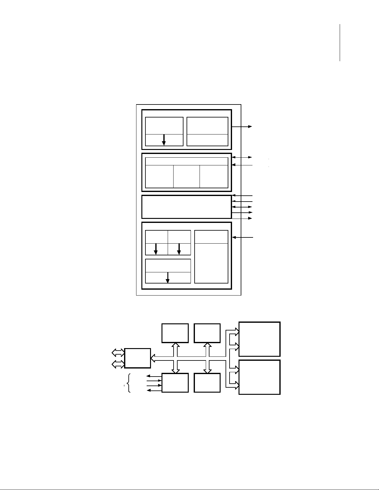
SCC/ESCC
Transmit Lo
g
Channel
A
Receive and Transmit Clock Mul
Transmit FIFO
NMOS/CMOS: 1 b
ESCC: 4 Bytes
Transmit M
U
Data Encoding & C
R
Generation
Digital
Phase-Lock
e
Loop
Baud Rat
Generat
o
Crystal
Oscillat
o
Amplifi
e
Modem/Control L
o
Receive M
U
CRC Checke
Data Decode
&
Sync Charac
t
Detection
Rec. Status
*
FIFO
Rec. Data*
FIFO
SDLC Frame Status F
10 x 19
Receive Lo
g
TxD
A
/TRxC
A
/RTxC
A
/CTS
A
/DCD
A
/SYNC
A
/RTS
A
/DTRA//RE
Q
RxD
A
Intern
a
Contro
Logic
Channel
A
Register
Channel
B
Register
Interru
p
Control
Logic
CPU & DM
A
Bus Interfa
c
Databu
Contr
o
Channel
A
Channel
B
/IN
/INTA
C
IE
IE
O
Interr
u
Contr
o
Exploded Vi
e
** See N
o
* NMOS/CMOS: 3 bytes each
ESCC: 8 bytes
** Not Available on NMOS
User Manual
6
UM010903-0515 General Description
SCC Block Diagram
Page 14

SCC/ESCC
User Manual
Pin Descriptions
The SCC pins are divided into seven functional groups: Address/Data, Bus Timing and Reset,
Device Control, Interrupt, Serial Data (both channels), Peripheral Control (both channels), and
Clocks (both channels). Figure on page 8 and Figure on page 9 display the pins in each functional
group for both Z80X30 and Z85X30. Notice the pin functions unique to each bus interface version
in the Address/Data group, Bus Timing and Reset group, and Control groups.
The Address/Data group consists of the bidirectional lines used to transfer data between the CPU
and the SCC (Addresses in the Z80X30 are latched by /AS). The direction of these lines depends
on whether the operation is a Read or Write.
7
The timing and control groups designate the type of transaction to occur and when it will occur.
The interrupt group provides inputs and outputs to conform to the Z-Bus
dling and prioritizing interrupts. The remaining groups are divided into channel A and channel B
groups for serial data (transmit or receive), peripheral control (such as DMA or modem), and the
input and output lines for the receive and transmit clocks.
®
specifications for han-
UM010903-0515 General Description
Page 15
SCC/ESCC
D7
D6
D5
D4
D3
D2
D1
D0
/RD
/WR
A//B
/CE
D//C
/INT
/INTACK
IEI
IEO
TxDA
RxDA
/TRxCA
/RTxCA
/SYNCA
/W//REQ
A
/DTR//REQA
/RTS
A
/CTS
A
/DCDA
TxDB
RxDB
/TRxCB
/RTxCB
/SYNCB
Serial
Data
Channel
Clocks
Channel
Controls
for Modem,
DMA and
Other
/W//REQB
/DTR//REQ
B
/RTS
B
/CTS
B
/DCDB
Interrup
t
Data Bus
Serial
Data
Channel
Clocks
Control
Bus Timing
and Reset
Channel
Controls
for Modem,
DMA and
Other
Z85X30
User Manual
The signal functionality and pin assignments (Figure on page 10 through Figure on page 13) stay
constant within the same bus interface group (i.e., Z80X30, Z85X30), except for some timing and/
or DC specification differences. For details, refer the individual product specifications.
8
UM010903-0515 General Description
Z85X30 Pin Functions
Page 16
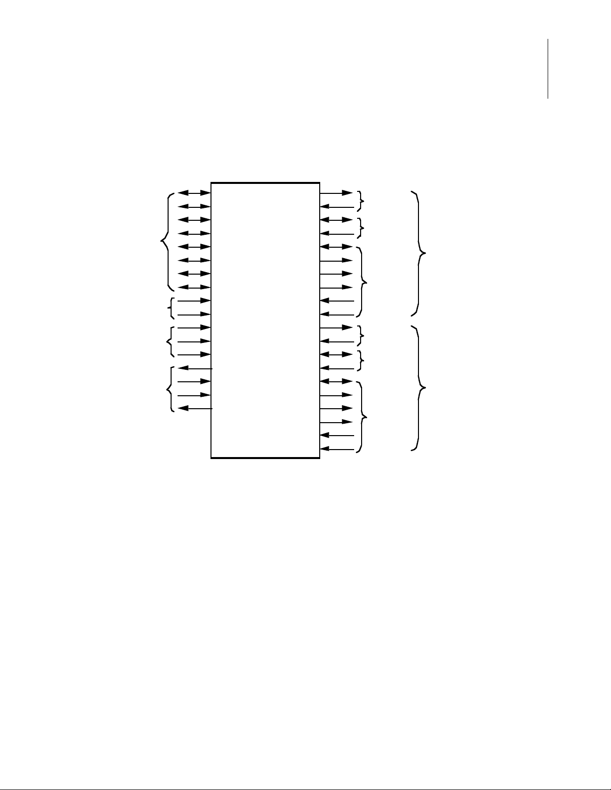
Pin Descriptions
AD7
AD6
AD5
AD4
AD3
AD2
AD1
AD0
/AS
/DS
R//W
CS1
/CS0
/INT
/INTACK
IEI
IEO
TxDA
RxDA
/TRxCA
/RTxCA
/SYNCA
/W//REQA
/DTR//REQA
/RTSA
/CTSA
/DCDA
TxDB
RxDB
/TRxCB
/RTxCB
/SYNCB
Serial
Data
Channel
Clocks
Channel
Controls
for Modem,
DMA and
Other
/W//REQB
/DTR//REQB
/RTSB
/CTSB
/DCDB
Interrupt
Address
Data Bus
Serial
Data
Channel
Clocks
Control
Bus Timing
and Reset
Channel
Controls
for Modem,
DMA and
Other
Z80X30
Channel A
Channel B
SCC/ESCC
User Manual
9
Z80x30 Pin Functions
UM010903-0515 General Description
Page 17
SCC/ESCC
1
2
9
3
4
5
6
7
8
4
0
39
3
8
3
7
3
6
35
3
4
3
3
32
D0
D2
D//C
D4
D6
/RD
/WR
A//B
/CE
D1
31
3
0
29
2
8
2
7
14
10
11
12
13
GND
/W//REQB
/SYNCB
/RTxCB
RxDB
D3
D5
D7
/INT
IEO
IEI
/INTACK
VCC
/W//REQA
/SYNCA
/RTxCA
RxDA
/TRxCA
TxDA
/DTR//REQA
/RTSA
/CTSA
/DCDA
PCL
K
15
16
17
18
19
20
/TRxCB
TxDB
/DTR//REQB
RTSB
/CTSB
/DCDB
2
6
25
2
4
2
3
22
21
Z85X30
User Manual
10
UM010903-0515 General Description
Z85X30 DIP Pin Assignments
Page 18

SCC/ESCC
User Manual
11
Z85X30 PLCC Pin Assignments
UM010903-0515 General Description
Page 19
SCC/ESCC
1
2
9
3
4
5
6
7
8
40
39
38
37
36
35
34
33
32
AD0
AD2
CS1
AD4
AD6
/DS
/AS
R//W
/CS0
AD1
31
30
29
28
27
14
10
11
12
13
GND
/W//REQB
/SYNCB
/RTxCB
RxDB
AD3
AD5
AD7
/INT
IEO
IEI
/INTACK
VCC
/W//REQA
/SYNCA
/RTxCA
RxDA
/TRxCA
TxDA
/DTR//REQA
/RTSA
/CTSA
/DCDA
PCL
K
15
16
17
18
19
20
/TRxCB
TxDB
/DTR//REQB
RTSB
/CTSB
/DCDB
26
25
24
23
22
21
Z80X30
User Manual
12
Z80X30 DIP Pin Assignments
UM010903-0515 General Description
Page 20

SCC/ESCC
1
User Manual
13
Z80X30 PLCC Pin Assignments
Pins Common to both Z85X30 and Z80X30
/CTSA, /CTSB. Clear To Send (inputs, active Low). These pins function as transmitter enables if
they are programmed for Auto Enable (WR3, D5=1). A Low on the inputs enables the respective
transmitters. If not programmed as Auto Enable, they may be used as general-purpose inputs. Both
inputs are Schmitt-trigger buffered to accommodate slow rise-time inputs. The SCC detects pulses
on these inputs and can interrupt the CPU on both logic level transitions.
/DCDA, /DCDB. Data Carrier Detect (inputs, active Low). These pins function as receiver
enables if they are programmed for Auto Enable (WR3, D5=1); otherwise, they are used as general-purpose input pins. Both pins are Schmitt-trigger buffered to accommodate slow rise time signals. The SCC detects pulses on these pins and can interrupt the CPU on both logic level
transitions.
/RTSA, /RTSB. Request To Send (outputs, active Low). The /RTS pins can be used as general-
purpose outputs or with the Auto Enable feature. When used with Auto Enable ON (WR3, D5=1)
in asynchronous mode, the /RTS pin goes High after the transmitter is empty. When Auto Enable
UM010903-0515 General Description
Page 21

SCC/ESCC
User Manual
is OFF, the /RTS pins are used as general-purpose outputs, and, they strictly follow the inverse
state of WR5, bit D1.
ESCC and 85C30:
In SDLC mode, the /RTS pins can be programmed to be deasserted when the closing flag of the
message clears the TxD pin, if WR7' D2 is set.
/SYNCA, /SYNCB. Synchronization (inputs or outputs, active Low). These pins can act either as
inputs, outputs, or part of the crystal oscillator circuit. In the Asynchronous Receive mode (crystal
oscillator option not selected), these pins are inputs similar to CTS and DCD. In this mode, transitions on these lines affect the state of the Synchronous/Hunt status bits in Read Register 0 but have
no other function. With the crystal oscillator option selected, these /SYNCA, /SYNCB pins
become the oscillator Xout pins and /RTxCA, /RTxCB pins
become the Xin pins, respectively.
14
In External Synchronization mode, with the crystal oscillator not sele
cted, these lines also act as
inputs. In this mode, /SYNC is driven Low to receive clock cycles after the last bit in the synchronous character is received. Character assembly begins on the rising edge of the receive clock
immediately preceding the activation of SYNC.
In the Internal Synchronization mode (Monosync and Bisync) with the crystal oscillator not
selected, these pins act as outputs and are active only during the part of the receive clock cycle in
which the synchronous condition is not latched. These outputs are active each time a synchronization pattern is recognized (regardless of character boundaries). In SDLC mode, the pins act as outputs and are valid on receipt of a flag. The /SYNC pins switch from input to output when
monosync, bisync, or SDLC is programmed in WR4 and sync modes are enabled.
/DTR//REQA, /DTR//REQB. Data Terminal Ready/Request (outputs, active Low). These pins
are programmable (WR14, D2) to serve either as general-purpose outputs or as DMA Request
lines. When programmed for DTR function (WR14 D2=0), these outputs follow the state programmed into the DTR bit of Write Register 5 (WR5 D7). When programmed for Ready mode,
these pins serve as DMA Requests for the transmitter.
ESCC and 85C30:
When used as DMA request lines (WR14, D2=1), the timing for the deactivation request can be
programmed in the added register, Write Register 7' (WR7') bit D4. If this bit is set, the /DTR//
REQ pin is deactivated with the same timing as the /W/REQ pin. If WR7' D4 is reset, the deactivation timing of /DTR//REQ pin is four clock cycles, the same as in the Z85C30.
/W//REQA, /W//REQB. Wait/Request (outputs, open-drain when programmed for Wait function,
driven High or Low when programmed for Ready function). These dual-purpose outputs may be
programmed as Request lines for a DMA controller or as Wait lines to synchronize the CPU to the
SCC data rate. The reset state is Wait.
RxDA, RxDB. Receive Data (inputs, active High). These input signals receive serial data at stan-
dard TTL levels.
/RTxCA, /R TxCB. Receive/Transmit Clocks (inputs, active Low). These pins can be programmed
to several modes of operation. In each channel, /RTxC may supply the receive clock, the transmit
UM010903-0515 General Description
Page 22

SCC/ESCC
User Manual
clock, the clock for the baud rate generator, or the clock for the Digital Phase-Locked Loop. These
pins can also be programmed for use with the respective SYNC pins as a crystal oscillator. The
receive clock may be 1, 16, 32, or 64 times the data rate in asynchronous modes. With the crystal
oscillator option selected, these /RTxCA, /RTxCB pins become the oscillator Xin pins and
/SYNCA, /SYNCB pins become the Xout pin
s, respectively.
15
TxDA, TxDB. Transmit
standard TTL levels.
/TRxCA, /TRxCB. Transmit/Receive Clocks (inputs or outputs, active Low). These pins can be
programmed in several different modes of operation. /TRxC may supply the receive clock or the
transmit clock in the input mode or supply the output of the Transmit Clock Counter (which parallels the Digital Phase-Locked Loop), the crystal oscillator, the baud rate generator, or the transmit
clock in the output mode.
PCLK. Clock (input). This is the master SCC clock used to synchronize internal signals. PCLK is
a TTL level signal. PCLK is not required to have any phase relationship with the master system
clock.
IEI. Interrupt Enable In (input, active High). IEI is used with IEO to form an interrupt daisy chain
when there is more than one interrupt driven device. A high IEI indicates that no other higher priority device has an interrupt under service or is requesting an interrupt.
IEO. Interrupt Enable Out (output, active High). IEO is High only if IEI is High and the CPU is
not servicing the SCC interrupt or the SCC is not requesting an interrupt (Interrupt Acknowledge
cycle only). IEO is connected to the next lower priority device’s IEI input and thus inhibits interrupts from lower priority devices.
/INT. Interrupt (output, open drain, active Low). This signal is activated when the SCC requests an
interrupt. Note that /INT is an open-drain output.
/INTACK. Interrupt Acknowledge (input, active Low). This is a strobe which indicates that an
interrupt acknowledge cycle is in progress. During this cycle, the SCC interrupt daisy chain is
resolved. The device is capable of returning an interrupt vector that may be encoded with the type
of interrupt pending. During the acknowledge cycle, if IEI is high, the SCC places the interrupt
vector on the databus when /RD goes active. /INTACK is latched by the rising edge of PCLK.
Data (outputs, active High). These output signals transmit serial data at
Pin Descriptions, (Z85X30 Only)
D7-D0. Data bus (bidirectional, tri-state). These lines carry data and commands to and from the
Z85X30.
/CE. Chip Enable (input, active Low). This signal selects the Z85X30 for a read or write opera-
tion.
/RD. Read (input, active Low). This signal indicates a read operation and when the Z85X30 is
selected, enables the Z85X30’s bus drivers. During the Interrupt Acknowledge cycle, /RD gates
the interrupt vector onto the bus if the Z85X30 is the highest priority device requesting an interrupt.
UM010903-0515 General Description
Page 23

SCC/ESCC
User Manual
/WR. Write (input, active Low). When the Z85X30 is selected, this signal indicates a write opera-
tion. This indicates that the CPU wants to write command bytes or data to the Z85X30 write registers.
A//B. Channel A/Channel B (input). This signal selects the channel in which the read or write
operation occurs. High selects channel A and Low selects channel B.
D//C. Data/Control Select (input). This signal defines the type of information transferred to or
from the Z85X30. High means data is being transferred and Low indicates a command.
Pin Descriptions, (Z80X30 Only)
AD7-AD0. Address/Data Bus (bidirectional, active High, tri-state). These multiplexed lines carry
register addresses to the Z80X30 as well as data or control information to and from the Z80X30.
R//W. Read//Write (input, read active High). This signal specifies whether the operation to be per-
formed is a read or a write.
16
/CS0. Chip Select 0 (input, active Low). This signal is latched concurrently with the addresses on
AD7-AD0 and must be active for the intended bus transaction to occur.
CS1. Chip Select 1 (input, active High). This second select signal must also be active before the
intended bus transaction can occur. CS1 must remain active throughout the transaction.
/DS. Data Strobe (input, active Low). This signal provides timing for the transfer of data into and
out of the Z80X30. If /AS and /DS are both Low, this is interpreted as a reset.
/AS. Address Strobe (input, active Low). Address on AD7AD0 are latched by the rising edge of
this signal.
UM010903-0515 General Description
Page 24

Interfacing the SCC/ESCC
Introduction
This chapter covers the system interface requirements with the SCC. Timing requirements for both
devices are described in a general sense here, and the user should refer to the SCC Product Specification for detailed AC/DC parametric requirements.
The ESCC and the 85C30 have an additional register, Write Register Seven Prime (WR7'). Its features include the ability to read WR3, WR4, WR5, WR7', and WR10. Both the ESCC and the
85C30 have the ability to deassert the /DTR//REG pin quickly to ease DMA interface design.
Additionally, the Z85230/L features a relaxed requirement for a valid data bus when the /WR pin
goes Low. The effects of the deeper data FIFOs should be considered when writing the interrupt
service routines. The user should read the sections which follow for details on these features.
SCC/ESCC
User Manual
17
Z80X30 Interface Timing
The Z-Bus compatible SCC is suited for system applications with multiplexed address/data buses
similar to the Z8
Two control signals, /AS and /DS, are used by the Z80X30 to time bus transactions. In addition,
four other control signals (/CS0, CS1, R//W, and /INTACK) are used to control the type of bus
transaction that occurs. A bus transaction is initiated by /AS; the rising edge latches the register
address on the Address/Data bus and the state of /INTACK and /CS0.
In addition to timing bus transactions, /AS is used by the interrupt section to set the Interrupt Pending (IP) bits.
Because of this, /AS must be kept cycling for the interrupt section to function properly.
The Z80X30 generates internal control signals in response to a register access. Since /AS and /DS
have no phase relationship with PCLK, the circuit generating these internal control signals provides time for metastable conditions to disappear. This results in a recovery time related to PCLK.
This recovery time applies only to transactions involving the Z80X30, and any intervening transactions are ignored. This recovery time is four PCLK cycles, measured from the falling edge of /
DS of one access to the SCC, to the falling edge of /DS for a subsequent access.
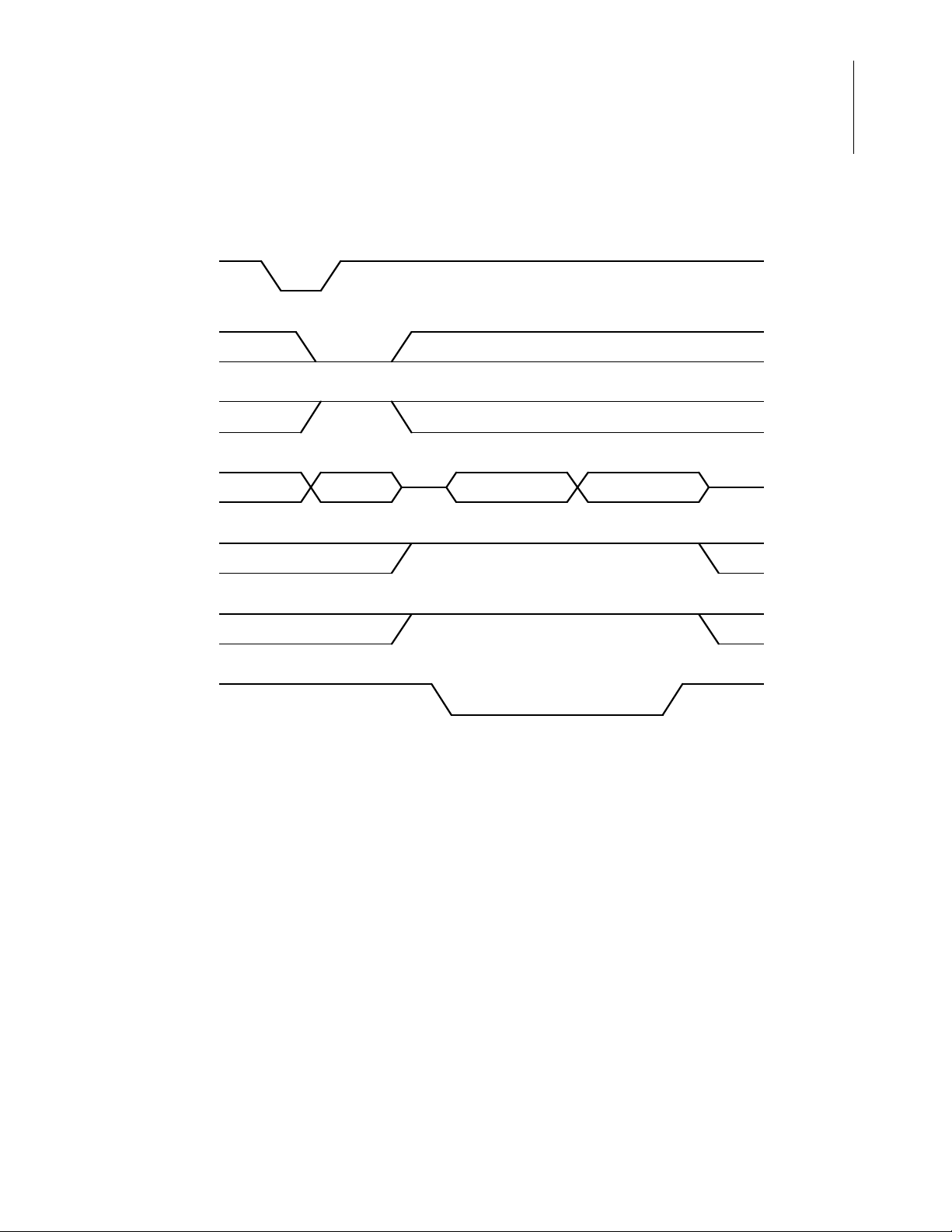
Z80X30 Read Cycle Timing
The read cycle timing for the Z80X30 is displayed in Figure . R//W must be High before /DS falls
to indicate a read The register address on AD7-AD0, as well as the state of cycle. The Z80X30
data bus drivers are enabled while CS1 /CS0 and /INTACK, are latched by the rising edge of /AS.
is High and /DS is Low.
®
, Z8000, and Z280.
UM010903-0515 Interfacing the SCC/ESCC
Page 25
SCC/ESCC
/AS
/CS0
/INTACK
AD7 - AD0
R//W
CS1
/DS
Address Data Valid
User Manual
18
Z80X30 Read Cycle
Z80X30 Write Cycle Timing
The write cycle timing for the Z80X30 is displayed in Figure on page 19. The register address on
AD7-AD0, as well as the state of /CS0 and /INTACK, are latched by the rising edge of /AS. R//W
must be Low when /DS falls to indicate a write cycle. The leading edge of the coincidence of CS1
High and /DS Low latches the write data on AD7-AD0, as well as the state of R//W.
UM010903-0515 Interfacing the SCC/ESCC
Page 26
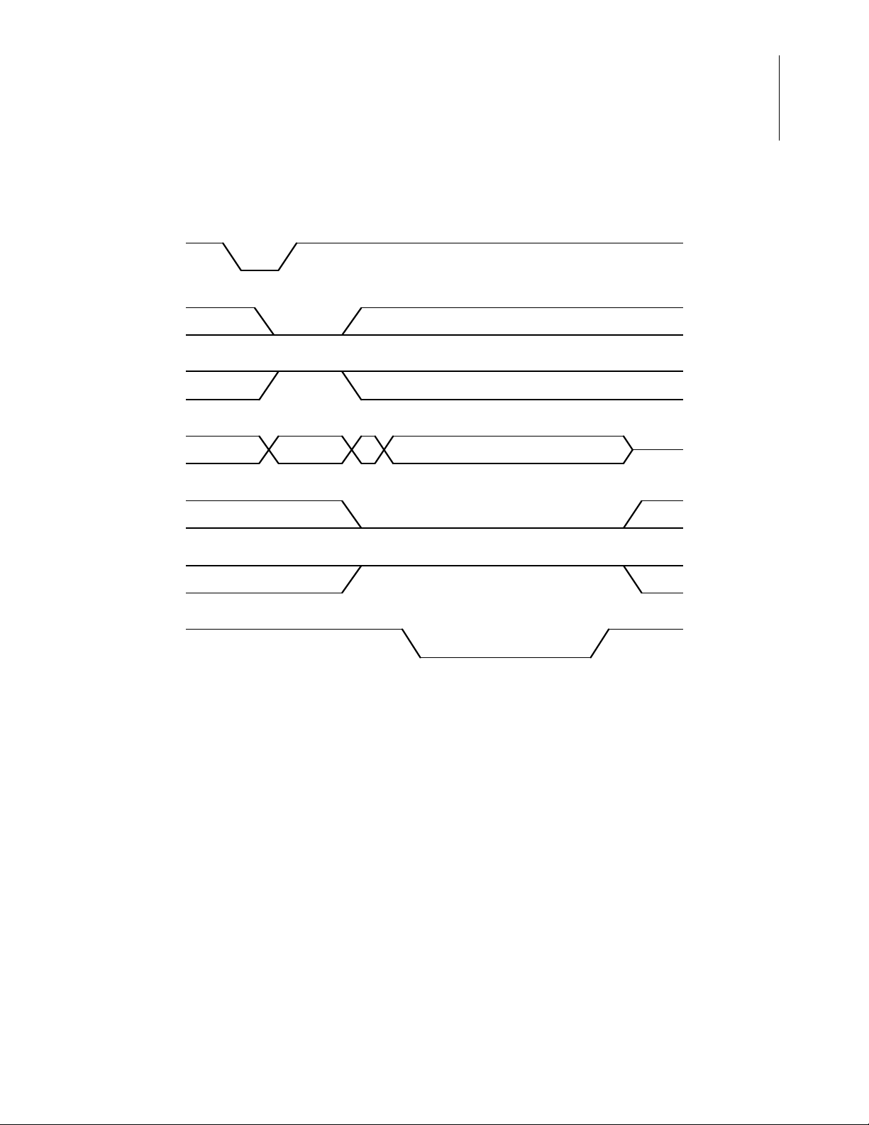
SCC/ESCC
Address Data Valid
/AS
/CS0
/INTACK
AD7 - AD0
R//W
CS1
/DS
User Manual
19
Z80X30 Write Cycle
Z80X30 Interrupt Acknowledge Cycle Timing
The interrupt acknowledge cycle timing for the Z80X30 is displayed in Figure on page 20. The
address on AD7-AD0 and the state of /CS0 and /INTACK are latched by the rising edge of /AS.
However, if /INTACK is Low, the address, /CS0, CS1 and R//W are ignored for the duration of the
interrupt acknowledge cycle.
UM010903-0515 Interfacing the SCC/ESCC
Page 27
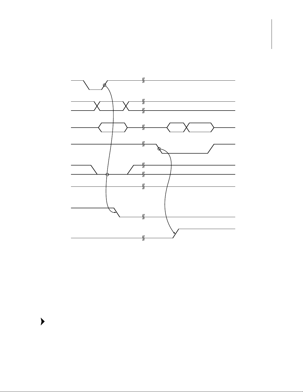
SCC/ESCC
/AS
/CS0
/DS
/INTACK
IEI
IEO
Vector
/INT
AD7 - AD0
Note:
User Manual
20
Z80X30 Interrupt Acknowledge Cycle
The Z80X30 samples the state of /INTACK on the rising edge of /AS, and AC parameters #7 and
#8 specify the setup and hold-time requirements. Between the rising edge of /AS and the falling
edge of /DS, the internal and external daisy chains settle (AC parameter #29). A system with no
external daisy chain should provide the time specified in spec #29 to settle the interrupt daisychain priority internal to the SCC. Systems using an external daisy chain should refer to Note 5
referenced in the Z80X30 Read/Write & Interrupt Acknowledge Timing for the time required to
settle the daisy chain.
/INTACK is sampled on the rising edge of /AS. If it does not meet the setup time to the
first rising edge of /AS of the interrupt acknowledge cycle, it is latched on the next ris-
UM010903-0515 Interfacing the SCC/ESCC
ing edge of /AS. Therefore, if /INTACK is asynchronous to /AS, it may be necessary to
add a PCLK cycle to the calculation for /INTACK to /RD delay time.
Page 28

SCC/ESCC
User Manual
If there is an interrupt pending in the SCC, and IEI is High when /DS falls, the acknowledge cycle was intended for the SCC. This being the case, the Z80X30 sets the Interrupt-UnderService (IUS) latch for the highest priority pending interrupt, as well as placing an interrupt vector
on AD7-AD0. The placing of a vector on the bus can be disabled by setting WR9, D1=1. The /INT
pin also goes inactive in response to the falling edge of /DS. Note that there should be only one /
DS per acknowledge cycle. Another important fact is that the IP bits in the Z80X30 are updated by
/AS, which may delay interrupt requests if the processor does not supply /AS strobes during the
time between accesses of the Z80X30.
Z80X30 Register Access
The registers in the Z80X30 are addressed via the address on AD7-AD0 and are latched by the rising edge of /AS. The Shift Right/Shift Left bit in the Channel B WR0 controls which bits are
decoded to form the register address. It is placed in this register to simplify programming when the
current state of the Shift Right/Shift Left bit is not known.
21
A hardware reset forces Shift Left mode where the address is decoded from AD5-AD1. In Shift
Right mode, the address is decoded from AD4-AD0. The Shift Right/Shift Left bit is written via a
command to make the software writing to WR0 independent of the state of the Shift Right/Shift
Left bit.
While in the Shift Left mode, the register address is placed on AD4-AD1 and the Channel Select
bit, A/B, is decoded from AD5. The register map for this case is listed in Table on page 21. In
Shift Right mode, the register address is again placed on AD4-AD1 but the channel select A/B is
decoded from AD0. The register map for this case is listed in Tabl e on page 23.
Because the Z80X30 does not contain 16 read registers, the decoding of the read registers is not
complete; this is listed in Tabl e on page 21 and Table on page 23 by parentheses around the register name. These addresses may also be used to access the read registers. Also, note that the
Z80X30 contains only one WR2 and WR9; these registers may be written from either channel.
Shift Left Mode is used when Channel A and B are to be programmed differently. This allows the
software to sequence through the registers of one channel at a time. The Shift Right Mode is used
when the channels are programmed the same. By incrementing the address, the user can program
the same data value into both the Channel A and Channel B register.
Z80X30 Register Map (Shift Left Mode)
READ 8030 80230
80C30/230* 80C30/230 WR15 D2=1
AD5 AD4 AD3 AD2 AD1 WRITE WR15 D2 = 0 WR15 D2=1 WR7' D6=1
0 0 0 0 0 WR0B RR0B RR0B RR0B
0 0 0 0 1 WR1B RR1B RR1B RR1B
UM010903-0515 Interfacing the SCC/ESCC
Page 29

SCC/ESCC
User Manual
Z80X30 Register Map (Shift Left Mode) (Continued)
READ 8030 80230
80C30/230* 80C30/230 WR15 D2=1
AD5 AD4 AD3 AD2 AD1 WRITE WR15 D2 = 0 WR15 D2=1 WR7' D6=1
0 0 0 1 0 WR2 RR2B RR2B RR2B
0 0 0 1 1 WR3B RR3B RR3B RR3B
0 0 1 0 0 WR4B (RR0B) (RR0B) (WR4B)
0 0 1 0 1 WR5B (RR1B) (RR1B) (WR5B)
0 0 1 1 0 WR6B (RR2B) RR6B RR6B
0 0 1 1 1 WR7B (RR3B) RR7B RR7B
0 1 0 0 0 WR8B RR8B RR8B RR8B
22
0 1 0 0 1 WR9 (RR13B) (RR13B) (WR3B)
0 1 0 1 0 WR10B RR10B RR10B RR10B
0 1 0 1 1 WR11B (RR15B) (RR15B) (WR10B)
0 1 1 0 0 WR12B RR12B RR12B RR12B
0 1 1 0 1 WR13B RR13B RR13B RR13B
0 1 1 1 0 WR14B RR14B RR14B (WR7’B)
0 1 1 1 1 WR15B RR15B RR15B RR15B
1 0 0 0 0 WR0A RR0A RR0A RR0A
1 0 0 0 1 WR1A RR1A RR1A RR1A
1 0 0 1 0 WR2 RR2A RR2A RR2A
1 0 0 1 1 WR3A RR3A RR3A RR3A
1 0 1 0 0 WR4A (RR0A) (RR0A) (WR4A)
1 0 1 0 1 WR5A (RR1A) (RR1A) (WR5A)
1 0 1 1 0 WR6A (RR2A) RR6A RR6A
1 0 1 1 1 WR7A (RR3A) RR7A RR7A
1 1 0 0 0 WR8A RR8A RR8A RR8A
1 1 0 0 1 WR9 (RR13A) (RR13A) (WR3A)
1 1 0 1 0 WR10A RR10A RR10A RR10A
1 1 0 1 1 WR11A (RR15A) (RR15A) (WR10A)
1 1 1 0 0 WR12A RR12A RR12A RR12A
UM010903-0515 Interfacing the SCC/ESCC
Page 30

SCC/ESCC
User Manual
Z80X30 Register Map (Shift Left Mode) (Continued)
READ 8030 80230
80C30/230* 80C30/230 WR15 D2=1
AD5 AD4 AD3 AD2 AD1 WRITE WR15 D2 = 0 WR15 D2=1 WR7' D6=1
1 1 1 0 1 WR13A RR13A RR13A RR13A
1 1 1 1 0 WR14A RR14A RR14A (WR7’A)
1 1 1 1 1 WR15A RR15A RR15A RR15A
Notes
1. The register names in () are the values read out from that register location.
2. WR15 bit D2 enables status FIFO function (not available on NMOS).
3. WR7' bit D6 enables extend read function (only on ESCC).
4. Includes 80C30/230 when WR15 D2=0.
23
Z80X30 Register Map (Shift Right Mode)
READ 8030 80230
80C30/230* 80C30/230 WR15 D2=1
AD4 AD3 AD2 AD1 AD0 WRITE WR15 D2 = 0 WR15 D2=1 WR7’ D6 =1
0 0 0 0 0 WR0B RR0B RR0B RR0B
0 0 0 0 1 WR0A RR0A RR0A RR0A
0 0 0 1 0 WR1B RR1B RR1B RR1B
0 0 0 1 1 WR1A RR1A RR1A RR1A
0 0 1 0 0 WR2 RR2B RR2B RR2B
0 0 1 0 1 WR2 RR2A RR2A RR2A
0 0 1 1 0 WR3B RR3B RR3B RR3B
0 0 1 1 1 WR3A RR3A RR3A RR3A
0 1 0 0 0 WR4B (RR0B) (RR0B) (WR4B)
0 1 0 0 1 WR4A (RR0A) (RR0A) (WR4A)
0 1 0 1 0 WR5B (RR1B) (RR1B) (WR5B)
0 1 0 1 1 WR5A (RR1A) (RR1A) (WR5A)
0 1 1 0 0 WR6B (RR2B) RR6B RR6B
0 1 1 0 1 WR6A (RR2A) RR6A RR6A
UM010903-0515 Interfacing the SCC/ESCC
Page 31

SCC/ESCC
User Manual
Z80X30 Register Map (Shift Right Mode) (Continued)
READ 8030 80230
80C30/230* 80C30/230 WR15 D2=1
AD4 AD3 AD2 AD1 AD0 WRITE WR15 D2 = 0 WR15 D2=1 WR7’ D6 =1
0 1 1 1 0 WR7B (RR3B) RR7B RR7B
0 1 1 1 1 WR7A (RR3A) RR7A RR7A
1 0 0 0 0 WR8B RR8B RR8B RR8B
1 0 0 0 1 WR8A RR8A RR8A RR8A
1 0 0 1 0 WR9 (RR13B) (RR13B) (WR3B)
1 0 0 1 1 WR9 (RR13A) (RR13A) (WR3A)
1 0 1 0 0 WR10B RR10B RR10B RR10B
24
1 0 1 0 1 WR10A RR10A RR10A RR10A
1 0 1 1 0 WR11B (RR15B) (RR15B) (WR10B)
1 0 1 1 1 WR11A (RR15A) (RR15A) (WR10A)
1 1 0 0 0 WR12B RR12B RR12B RR12B
1 1 0 0 1 WR12A RR12A RR12A RR12A
1 1 0 1 0 WR13B RR13B RR13B RR13B
1 1 0 1 1 WR13A RR13A RR13A RR13A
1 1 1 0 0 WR14B RR14B RR14B (WR7’B)
1 1 1 0 1 WR14A RR14A RR14A (WR7’A)
1 1 1 1 0 WR15B RR15B RR15B RR15B
1 1 1 1 1 WR15A RR15A RR15A RR15A
Notes
1. The register names in () are the values read out from that register location.
2. WR15 bit D2 enables status FIFO function (not available on NMOS).
3. WR7' bit D6 enables extend read function (only on ESCC).
4. * Includes 80C30/230 when WR15 D2=0.
Z80C30 Register Enhancement
The Z80C30 has an enhancement to the NMOS Z8030 register set, which is the addition of a
10x19 SDLC Frame Status FIFO. When WR15 bit D2=1, the SDLC Frame Status FIFO is
enabled, and it changes the functionality of RR6 and RR7. See Section SDLC Frame Status FIFO
on page 126 for more details on this feature.
UM010903-0515 Interfacing the SCC/ESCC
Page 32

SCC/ESCC
D7 D6 D5 D4 D3 D2 D1 D0
WR7'
Auto Tx Flag
Auto EOM Reset
Auto RTS Turnoff
Rx FIFO Half Full
DTR/REQ Timing
M
Tx FIFO Empty
External Read Ena
b
0
User Manual
Z80230 Register Enhancements
In addition to the Z80C30 enhancements, the 80230 has several enhancements to the SCC register
set. These include the addition of Write Register 7 Prime (WR7'), and the ability to read registers
that are read only in the 8030.
Write Register 7' is addressed by setting WR15 bit, D0=1 and then addressing WR7. Figure displays the register bit location of the six features enabled through this register. All writes to address
seven are to WR7' when WR15, D0=1. Refer to Register Descriptions on page 136 for detailed
information on WR7'.
25
WR7' bit D6=1, enables the extended read register capability. This allows the user to read the contents of WR3, WR4, WR5, WR7' and WR10 by reading RR9, RR4, RR5, RR14 and RR11, respectively. When WR7' D6=0, these write registers are write only.
Table lists what functions are enabled for the various combinations of register bit enables. See
Table on page 21 (Shift Left) and Table on page 23 (Shift Right) for the register address map with
the SDLC FIFO enabled only and the map with both the extended read and SDLC FIFO features
UM010903-0515 Interfacing the SCC/ESCC
enabled.
Write Register 7 Prime (WR7')
Page 33

SCC/ESCC
User Manual
Z80230 SDLC/HDLC Enhancement Options
WR15 WR7’
Bit D2 Bit D0 Bit D6 Functions Enabled
0 1 0 WR7' enabled only
0 1 1 WR7' with extended read enabled
1 0 X 10x19 SDLC FIFO enhancement enabled only
1 1 0 10x19 SDLC FIFO and WR7'
1 1 1 10x19 SDLC FIFO and WR7' with extended read
enabled
26
Z80X30 Reset
The Z80X30 may be reset by either a hardware or software reset. Hardware reset occurs when /AS
and /DS are both Low at the same time, which is normally an illegal condition.
As long as both /AS and /DS are Low, the Z80X30 recognizes the reset condition. However, once
this condition is removed, the reset condition is asserted internally for an additional four to five
PCLK cycles. During this time, any attempt to access is ignored.
The Z80X30 has three software resets that are encoded into two command bits in WR9. There are
two channel resets, which only affect one channel in the device and some bits of the write registers. The command forces the same result as the hardware reset, the Z80X30 stretches the reset
signal an additional four to five PCLK cycles beyond the ordinary valid access recovery time. The
bits in WR9 may be written at the same time as the reset command because these bits are affected
only by a hardware reset. The reset values of the various registers are listed in Tab l e .
Z80X30 Register Reset Values
Hardware RESET Channel RESET
76543 210 765432 10
WR0 000 00 00 0 00 00 00 00
WR1 0 0 X 0 0 X 0 0 0 0 X 0 0 X 0 0
WR2 XXX XX XX X XX XX XX XX
WR3 XXX XX XX 0 XX XX XX X0
WR4 X X X X X 1 X X X X X X X 1 X X
WR5 0XX00 00 X 0 XX0 00 0X
UM010903-0515 Interfacing the SCC/ESCC
Page 34

User Manual
Z80X30 Register Reset Values (Continued)
Hardware RESET Channel RESET
76543 210 765432 10
WR6 XXX XX XX X XX XX XX XX
WR7 XXX XX XX X XX XX XX XX
WR7'* 001 00 00 0 0 0 10 00 00
WR9 110 00 0XX XX 0XXX XX
WR10 00000 000 0XX000 00
WR11 00001000 XXXXXX XX
WR12 XXXXXXXX XXXXXX XX
WR13 XXXXXXXX XXXXXX XX
SCC/ESCC
27
WR14 XX110000 XX1000 XX
WR15 11111 000 111110 00
RR0 X 1 X X X 1 0 0 X 1 X X X 1 0 0
RR1 000 00 11 X 0 0 00 01 1X
RR3 000 00 00 0 0 0 00 00 00
RR10 0X000000 0X0000 00
Note: *WR7' is available only on the Z80230.
Z85X30 Interface Timing
Two control signals, /RD and /WR, are used by the Z85X30 to time bus transactions. In addition,
four other control signals, /CE, D//C, A//B and /INTACK, are used to control the type of bus transaction that occurs. A bus transaction starts when the addresses on D//C and A//B are asserted
before /RD or /WR fall (AC Spec #6 and #8). The coincidence of /CE and /RD or /CE and /WR
latches the state of D//C and A//B and starts the internal operation. The /INTACK signal must have
been previously sampled High by a rising edge of PCLK for a read or write cycle to occur. In addition to sampling /INTACK, PCLK is used by the interrupt section to set the IP bits.
The Z85X30 generates internal control signals in response to a register access. Since /RD and /WR
have no phase relationship with PCLK, the circuitry generating these internal control signals provides time for metastable conditions to disappear. This results in a recovery time related to PCLK.
This recovery time applies only between transactions involving the Z85X30, and any intervening
transactions are ignored. This recovery time is four PCLK cycles (AC Spec #49), measured from
the falling edge of /RD or /WR in the case of a read or write of any register.
UM010903-0515 Interfacing the SCC/ESCC
Page 35

SCC/ESCC
A//B, D//C
/INTACK
/CE
/RD
D7-D0
Address Valid
Data Valid
User Manual
Z85X30 Read Cycle Timing
The read cycle timing for the Z85X30 is displayed in Figure on page 28. The address on A//B and
D//C is latched by the coincidence of /RD and /CE active. /CE must remain Low and /INTACK
must remain High throughout the cycle. The Z85X30 bus drivers are enabled while /CE and /RD
are both Low. A read with D//C High does not disturb the state of the pointers and a read cycle
with D//C Low resets the pointers to zero after the internal operation is complete
28
Z85X30 Read Cycle Timing
Z85X30 Write Cycle Timing
The write cycle timing for the Z85X30 is displayed in Figure on page 29. The address on A//B
and D//C, as well as the data on D7-D0, is latched by the coincidence of /WR and /CE active. /CE
must remain Low and /INTACK must remain High throughout the cycle. A write cycle with D//C
High does not disturb the state of the pointers and a write cycle with D//C Low resets the pointers
to zero after the internal operation is complete.
Historically, the NMOS/CMOS version latched the data bus on the falling edge of /WR. However,
many CPUs do not guarantee that the data bus is valid at the time when the /WR pin goes low, so
the data bus timing was modified to allow a maximum delay from the falling edge of /WR to the
latching of the data bus. On the Z85230/L, the AC Timing parameter #29 TsDW(WR), Write Data
to /WR falling minimum, has been changed to: /WR falling to Write Data Valid maximum. Refer
to the AC Timing Characteristic section of the Z85230/L Product Specification for more information regarding this change.
UM010903-0515 Interfacing the SCC/ESCC
Page 36

SCC/ESCC
A//B, D//C
/INTACK
/CE
/WR
D7-D0
Address Valid
Data Valid
See Note
Note: Dotted line is ESCC only.
/INTACK
/RD
D7-D0 Vector
User Manual
29
Z85X30 Write Cycle Timing
Z85X30 Interrupt Acknowledge Cycle Timing
The interrupt acknowledge cycle timing for the Z85X30 is displayed in Figure on page 29. The
state of /INTACK is latched by the rising edge of PCLK (AC Spec #10). While /INTACK is Low,
the state of A//B, /CE, D//C, and /WR are ignored.
Z85X30 Interrupt Acknowledge Cycle Timing
UM010903-0515 Interfacing the SCC/ESCC
Page 37

SCC/ESCC
Note:
Notes:
User Manual
Between the time /INTACK is first sampled Low and the time /RD falls, the internal and external
IEI/IEO daisy chain settles (AC parameter #38 TdIAI(RD) Note 5). A system with no external
daisy chain must provide the time specified in AC Spec #38 to settle the interrupt daisy chain priority internal to the SCC. Systems using the external IEI/IEO daisy chain should refer to Note 5
referenced in the Z85X30 Read/Write and Interrupt Acknowledge Timing for the time required to
settle the daisy chain.
/INTACK is sampled on the rising edge of PCLK. If it does not meet the setup time to the
first rising edge of PCLK of the interrupt acknowledge cycle, it is latched on the next rising
edge of PCLK. Therefor e, if /INTACK is asynchronous to PCLK, it may be necessary to add
a PCLK cycle to the calculation for /INTACK to /RD delay time.
If there is an interrupt pending in the Z85X30, and IEI is High when /RD falls, the interrupt
acknowledge cycle was intended for the Z85X30. In this case, the Z85X30 sets the appropriate
Interrupt-Under-Service latch, and places an interrupt vector on D7-D0.
30
If the falling edge of /RD sets an IUS bit in the Z85X30, the /INT pin goes inactive in response to
the falling edge. Note that there should be only one /RD per acknowledge cycle.
1. The IP bits in the Z85X30 are updated by PCLK. However, when the register pointer is
pointing to RR2 and RR3, the IP bits are prevented from changing. This pr events data
changing during a read, but will delay interrupt requests if the pointers are left pointing at these registers.
2. The SCC should only receive one INT ACK signal per acknowledge cycle. Ther efore, if
the CPU generates more than one (as is common for the 80X86 family), an external
circuit should be used to convert this into a single pulse or does not use Interrupt
Acknowledge.
Z85X30 Register Access
The registers in the Z85X30 are accessed in a two step process, using a Register Pointer to perform
the addressing. To access a particular register, the pointer bits are set by writing to WR0. The
pointer bits may be written in either channel because only one set exists in the Z85X30. After the
pointer bits are set, the next read or write cycle of the Z85X30 having D//C Low will access the
desired register. At the conclusion of this read or write cycle the pointer bits are reset to 0s, so that
the next control write is to the pointers in WR0.
A read to RR8 (the receive data FIFO) or a write to WR8 (the transmit data FIFO) is either done in
this fashion or by accessing the Z85X30 having D//C pin High. A read or write with D//C High
accesses the data registers directly, and independently of the state of the pointer bits. This allows
single-cycle access to the data registers and does not disturb the pointer bits.
The fact that the pointer bits are reset to 0, unless explicitly set otherwise, means that WR0 and
RR0 may also be accessed in a single cycle. That is, it is not necessary to write the pointer bits
with 0 before accessing WR0 or RR0.
UM010903-0515 Interfacing the SCC/ESCC
Page 38

SCC/ESCC
User Manual
There are three pointer bits in WR0, and these allow access to the registers with addresses 7
through 0. Note that a command may be written to WR0 at the same time that the pointer bits are
written. To access the registers with addresses 15 through 8, the Point High command must
accompany the pointer bits. This precludes concurrently issuing a command when pointing to
these registers.
The register map for the Z85X30 is listed in Table on page 31. If, for some reason, the state of the
pointer bits is unknown they may be reset to 0 by performing a read cycle with the D//C pin held
Low. Once the pointer bits have been set, the desired channel is selected by the state of the A//B
pin during the actual read or write of the desired register.
Z85X30 Register Map
Read 8530
85C30/230 85C30/230 WR15 D2=1
31
A//B PNT2 PNT1 PNT0 WRITE WR15 D2 = 0 WR15 D2=1 WR7' D6=1
0 0 0 0 WR0B RR0B RR0B RR0B
0 0 0 1 WR1B RR1B RR1B RR1B
0 0 1 0 WR2 RR2B RR2B RR2B
0 0 1 1 WR3B RR3B RR3B RR3B
0 1 0 0 WR4B (RR0B) (RR0B) (WR4B)
0 1 0 1 WR5B (RR1B) (RR1B) (WR5B)
0 1 1 0 WR6B (RR2B) RR6B RR6B
0 1 1 1 WR7B (RR3B) RR7B RR7B
1 0 0 0 WR0A RR0A RR0A RR0A
1 0 0 1 WR1A RR1A RR1A RR1A
1 0 1 0 WR2 RR2A RR2A RR2A
1 0 1 1 WR3A RR3A RR3A RR3A
1 1 0 0 WR4A (RR0A) (RR0A) (WR4A)
1 1 0 1 WR5A (RR1A) (RR1A) (WR5A)
1 1 1 0 WR6A (RR2A) RR6A RR6A
1 1 1 1 WR7A (RR3A) RR7A RR7A
With Point High Command
0 0 0 0 WR8B RR8B RR8B RR8B
0 0 0 1 WR9 (RR13B) (RR13B) (WR3B)
UM010903-0515 Interfacing the SCC/ESCC
Page 39

User Manual
Z85X30 Register Map (Continued)
Read 8530
85C30/230 85C30/230 WR15 D2=1
A//B PNT2 PNT1 PNT0 WRITE WR15 D2 = 0 WR15 D2=1 WR7' D6=1
0 0 1 0 WR10B RR10B RR10B RR10B
0 0 1 1 WR11B (RR15B) (RR15B) (WR10B)
0 1 0 0 WR12B RR12B RR12B RR12B
0 1 0 1 WR13B RR13B RR13B RR13B
0 1 1 0 WR14B RR14B RR14B (WR7’B)
0 1 1 1 WR15B RR15B RR15B RR15B
1 0 0 0 WR8A RR8A RR8A RR8A
SCC/ESCC
32
1 0 0 1 WR9 (RR13A) (RR13A) (WR3A)
1 0 1 0 WR10A RR10A RR10A RR10A
1 0 1 1 WR11A (RR15A) (RR15A) (WR10A)
1 1 0 0 WR12A RR12A RR12A RR12A
1 1 0 1 WR13A RR13A RR13A RR13A
1 1 1 0 WR14A RR14A RR14A (WR7’A)
1 1 1 1 WR15A RR15A RR15A RR15A
Notes
1. WR15 bit D2 enables status FIFO function. (Not available on NMOS).
2. WR7' bit D6 enables extend read function. (Only on ESCC and 85C30).
Z85C30 Register Enhancement
The Z85C30 has an enhancement to the NMOS Z8530 register set, which is the addition of a
10x19 SDLC Frame Status FIFO. When WR15 bit D2=1, the SDLC Frame Status FIFO is
enabled, and it changes the functionality of RR6 and RR7. See SDLC Frame Status FIFO on page
126 for more details on this feature.
Z85C30/Z85230/L Register Enhancements
In addition to the enhancements mentioned in Z85C30 Register Enhancement on page 32, the
85C30/85230/L provides several enhancements to the SCC register set. These include the addition
of Write Register 7 Prime (WR7'), the ability to read registers that are write-only in the SCC.
Write Register 7' is addressed by setting WR15, D0=1 and then addressing WR7. Figure and
Figure on page 33 displays the register bit location of the six features enabled through this register
UM010903-0515 Interfacing the SCC/ESCC
Page 40

SCC/ESCC
D7 D6 D5 D4 D3 D2 D1 D0
WR7'
Auto Tx Flag
Auto EOM Reset
Auto/RTS Deactivation
Rx FIFO Half Full
DTR/REQ Timing Mode
Tx FIFO Empty
Extended Read Enable
Reserved (Must be 0)
D7 D6 D5 D4 D3 D2 D1 D0
WR7' Prime
Auto Tx Flag
Auto EOM Reset
Auto/RTS Deactivation
Force TxD High
/DTR//REQ Fast Mode
Complete CRC Reception
Extended Read Enable
Reserved (Program as 0)
User Manual
for the 85230/L, while Figure on page 29 displays the register bit location for the 85C30. Note
that the difference between the two WR7' registers for the 85230/L and the 85C30 is bit D5 and bit
D4. All writes to address seven are to WR7' when WR15 D0=1. Refer to Register Descriptions on
page 136 for detailed information on WR7'.
33
UM010903-0515 Interfacing the SCC/ESCC
Write Register 7 Prime (WR7') for the 85230/L
Write Register 7 Prime for the 85C30
Page 41

SCC/ESCC
User Manual
Setting WR7' bit D6=1 enables the extended read register capability. This allows the user to read
the contents of WR3, WR4, WR5, WR7' and WR10 by reading RR9, RR4, RR5, RR14 and RR11,
respectively. When WR7' D6=0, these write registers are write-only.
Table lists what functions are enabled for the various combinations of register bit enables. See
Table on page 31 for the register address map with only the SDLC FIFO enabled and with both
the extended read and SDLC FIFO features enabled.
Z85C30/Z85230/L Register Enhancement Options
WR15 WR7’
Bit D2 Bit D0 Bit D6 Functions Enabled
0 1 0 WR7' enabled only
0 1 1 WR7' with extended read enabled
34
1 0 X 10x19 SDLC FIFO enhancement enabled only
1 1 0 10x19 SDLC FIFO and WR7'
1 1 1 10x19 SDLC FIFO and WR7' with extended read
enabled
Z85X30 Reset
The Z85X30 may be reset by either a hardware or software reset. Hardware reset occurs when /
WR and /RD are both Low at the same time, which is normally an illegal condition.
As long as both /WR and /RD are Low, the Z85X30 recognizes the reset condition. However, once
this condition is removed, the reset condition is asserted internally for an additional four to five
PCLK cycles. During this time any attempt to access is ignored.
The Z85X30 has three software resets that are encoded into the command bits in WR9. There are
two channel resets which only affect one channel in the device and some bits of the write registers.
The command forces the same result as the hardware reset, the Z85X30 stretches the reset signal
an additional four to five PCLK cycles beyond the ordinary valid access recovery time. The bits in
WR9 may be written at the same time as the reset command because these bits are affected only by
a hardware reset. The reset values of the various registers are listed in Table .
UM010903-0515 Interfacing the SCC/ESCC
Page 42

SCC/ESCC
User Manual
35
Z85X30 Register Reset Value
Hardware RESET Channel RESET
7 6543 210 76543 210
WR00 000 0 0 0 0 0 0000 0 0 0
WR1 0 0 X 0 0 X 0 0 0 0 X 0 0 X 0 0
WR2 X XX X X X X X X XXXX X X X
WR3 X XX X X X X 0 X XXXX X X 0
WR4 X XX X X 1 X X XXXXX 1 X X
WR5 0 XX 0 0 0 0 X 0 XX00 0 0 X
WR6 X XX X X X X X X XXXX X X X
WR7 X XX X X X X X X XXXX X X X
WR7'*0 01 0 0 0 0 0 0 0100 0 0 0
WR91 100 0 0 XX XX0XX XXX
WR100 0000 000 0XX00 000
WR110 0001 000 XXXXX XXX
WR12X XXXX XXX XXXXX XXX
WR13X XXXX XXX XXXXX XXX
WR14X X110 000 XX100 0XX
WR151 1111 000 11111 000
RR0X 1XXX100 X1XXX100
RR1 0 00 0 0 1 1 X 00000 1 1 X
RR3 0 00 0 0 0 0 0 00000 0 0 0
RR100 X000 000 0X000 000
Note: *WR7' is only available on the 85C30 and the ESCC.
Interface Programming
The following subsections explain and illustrate all areas of interface programming.
UM010903-0515 Interfacing the SCC/ESCC
Page 43

SCC/ESCC
User Manual
I/O Programming Introduction
The SCC can work with three basic forms of I/O operations: polling, interrupts, and block transfer.
All three I/O types involve register manipulation during initialization and data transfer. However,
the interrupt mode also incorporates Z-Bus interrupt protocol for a fast and efficient data transfer.
Regardless of the version of the SCC, all communication modes can use a choice of polling, interrupt and block transfer. These modes are selected by the user to determine the proper hardware and
software required to supply data at the rate required.
Note to ESCC Users: Those familiar with the NMOS/CMOS version will find the ESCC I/O
operations very similar but should note the following differences: the addition of software
acknowledge (which is available in the current version of the CMOS SCC, but not in NMOS); the
/DTR//REQ pin can be programmed to be deasserted faster; and the programmability of the data
interrupts to the FIFO fill level.
Polling
36
This is the simplest mode to implement. The software must poll the SCC to determine when data is
to be input or output from the SCC. In this mode, MIE (WR9, bit 3), and Wait/DMA Request
Enable (WR1, bit 7) are both reset to 0 to disable any interrupt or DMA requests. The software
must then poll RR0 to determine the status of the receive buffer, transmit buffer and external status.
During a polling sequence, the status of Read Register 0 is examined in each channel. This register
indicates whether or not a receive or transmit data transfer is needed and whether or not any special conditions are present, e.g., errors.
This method of I/O transfer avoids interrupts and, consequently, all interrupt functions should be
disabled. With no interrupts enabled, this mode of operation must initiate a read cycle of Read
Register 0 to detect an incoming character before jumping to a data handler routine.
Interrupts
Each of the SCC’s two channels contain three sources of interrupts, making a total of six interrupt
sources. These three sources of interrupts are: 1) Receiver, 2) Transmitter, and 3) External/Status
conditions. In addition, there are several conditions that may cause these interrupts. Figure on
page 37 displays the different conditions for each interrupt source and each is enabled under program control. Channel A has a higher priority than Channel B with Receive, Transmit, and External/Status Interrupts prioritized, respectively, within each channel as listed in Table . The SCC
internally updates the interrupt status on every PCLK cycle in the Z85X30 and on /AS in the
Z80X30.
Interrupt Source Priority
Receive Channel A Highest
Transmit Channel A
UM010903-0515 Interfacing the SCC/ESCC
Page 44

Interrupt Source Priority (Continued)
SCC
Interrupt
Receiver
Interrupt
Sources
Zero Count
Transmit Buffer Empty
Parity Error (If enabled)
End of Frame (SDLC)
Framing Error
Receive Overrun
DCD
SYNC/HUNT
CTS
Tx Underrun/EOM
Break/Abort
Transmitter
Interrupt
Source
External/Status
Interrupt
Sources
INT on all Rx Character
or Special Condition
Rx Interrupt on Special
Condition Only
INT on first Rx Character
or Special Condition
Receive Character Available
External/Status Channel A
Receive Channel B
Transmit Channel B
External/Status Channel B Lowest
SCC/ESCC
User Manual
37
ESCC:
UM010903-0515 Interfacing the SCC/ESCC
The receive interrupt request is either caused by a receive character available or a special condition. When the receive character available interrupt is generated, it is dependent on WR7' bit
ESCC Interrupt Sources
Page 45

SCC/ESCC
Note:
User Manual
D3. If WR7' D3=0, the receive character available interrupt is generated when one character is
loaded into the FIFO and is ready to be read. If WR7' D3=1, the receive character available
interrupt is generated when four bytes are available to be read in the receive data FIFO. The
programmed value of WR7' D5 also affects how DMA requests are generated. See Block/DMA
Transfer on page 60 for details.
If the ESCC is used in SDLC mode, it enables the SDLC Status FIFO to affect how
receive interrupts are generated. If this featur e is used, r ead SDLC Frame Status FIFO
on page 126 on the SDLC Anti-Lock Feature.
The special conditions are Receive FIFO overrun, CRC/framing error, end of frame, and
parity. If parity is included as a special condition, it is dependent on WR1 D2. The special
condition status can be read from RR1.
On the NMOS/CMOS versions, set the IP bit whenever the transmit buffer becomes
empty. This means that the transmit buffer was full before the transmit IP can be set.
38
ESCC:
The transmit interrupt request has only one source and is dependent on WR7' D5. If the IP bit
WR7' D5=0, it is set when the transmit buffer becomes completely empty. If IP bit WR7' D5=1,
the transmit interrupt is generated when the entry location of the FIFO is empty. Note that in
both cases the transmit interrupt is not set until after the first character is written to the ESCC.
For more information on Transmit Interrupts, see Transmit Interrupts and Transmit Buffer Empty
Bit on page 49 for details.
The External/status interrupts have several sources which may be individually enabled in WR15.
The sources are zero count, /DCD, Sync/Hunt, /CTS, transmitter under-run/EOM and Break/
Abort.
Interrupt Control
In addition to the MIE bit that enables or disables all SCC interrupts, each source of interrupt in
the SCC has three control/status bits associated with it. They are the Interrupt Enable (IE), Interrupt Pending (IP), and Interrupt-Under-Service (IUS). Figure on page 39 displays the SCC inter-
rupt structure.
UM010903-0515 Interfacing the SCC/ESCC
Page 46

SCC/ESCC
IE
Interrupt Vector
From
CPU
Status
Decoder
MIE DLC
IP IUS
IEI /INT IEO/INTACK
from Pullup
Resistor or IEO
line of Highe
r
Priority Device
To CPU
To IEI Input of
Lower Priority
Device
IE
Channel A
Receiver
(Highest Priority)
from
IEI
Pin
IUSIP IE
Channel A
Transmitter
IUSIP
IEI IEO IEI IEO
IE
Channel A
External/Status
Conditions
IUSIP
IEI IEO
IE
Channel B
Receiver
IUSIP IE
Channel B
Transmitter
IUSIP
IEI IEO IEI IEO
IE
Channel B
External/Status
Conditions
(Lowest
Priority)
IUSIP
IEI IEO
To
IEO
Pin
User Manual
39
Peripheral Interrupt Structure
Figure displays the internal priority resolution method to allow the highest priority interrupt to be
serviced first. Lower priority devices on the external daisy chain can be prevented from requesting
interrupts via the Disable Lower Chain bit in WR9 D2.
Internal Priority Resolution
UM010903-0515 Interfacing the SCC/ESCC
Page 47

SCC/ESCC
D7 D6 D5 D4 D3 D2 D1 D0
Channel B Ext/Stat
Read Register 3
Channel B Tx IP
Channel B Rx IP
Channel A Ext/Stat
Channel A Tx IP
Channel A Rx IP
0
0
* Always 0 In B Channel
User Manual
Master Interrupt Enable Bit
The Master Interrupt Enable (MIE) bit, WR9 D3, must be set to enable the SCC to generate interrupts. The MIE bit should be set after initializing the SCC registers and enabling the individual
interrupt enables. The SCC requests an interrupt by asserting the /INT pin Low from its opendrain state only upon detection that one of the enabled interrupt conditions has been detected.
Interrupt Enable Bit
The Interrupt Enable (IE) bits control interrupt requests from each interrupt source on the SCC. If
the IE bit is set to 1 for an interrupt source, that source may generate an interrupt request, providing all of the necessary conditions are met. If the IE bit is reset, no interrupt request is generated by
that source. The transmit interrupt IE bit is WR1 D1. The receive interrupt IE bits are WR1 D3 and
D4. The external status interrupts are individually enabled in WR15 with the master external status
interrupt enable in WR1 D0. Reminder: The MIE bit, WR9 D3, must be set for any interrupt to
occur.
40
Interrupt Pending Bit
The Interrupt Pending (IP) bit for a given source of interrupt is set by the presence of an interrupt
condition in the SCC. It is reset directly by the processor, or indirectly by some action that the processor may take. If the corresponding IE bit is not set, the IP for that source of interrupt will never
be set. The IP bits in the SCC are read only via RR3 as displayed in Figure .
The Interrupt-Under-Service (IUS) bits are completely hidden from the processor. An IUS bit is
set during an interrupt acknowledge cycle for the highest priority IP. On the CMOS or ESCC, the
UM010903-0515 Interfacing the SCC/ESCC
RR3 Interrupt Pending Bits
Interrupt-Under-Service Bit
Page 48

SCC/ESCC
Note:
User Manual
IUS bits can be set by either a hardware acknowledge cycle with the /INTACK pin or through software if WR9 D5=1 and then reading RR2.
The IUS bits control the operation of internal and external daisy-chain interrupts. The internal
daisy chain links the six sources of interrupt in a fixed order, chaining the IUS bit of each source.
If an internal IUS bit is set, all lower priority interrupt requests are masked off; during an interrupt
acknowledge cycle the IP bits are also gated into the daisy chain. This ensures that the highest priority IP selected has its IUS bit set. At the end of an interrupt service routine, the processor must
issue a Reset Highest IUS command in WR0 to re-enable lower priority interrupts. This is the only
way, short of a software or hardware reset, that an IUS bit may be reset.
It is not necessary to issue the Reset Highest IUS command in the interrupt service routine, since the IUS bits can only be set by an interrupt acknowledge if no hardware
acknowledge or software acknowledge cycle (not with NMOS) is executed. The only
exception is when the SDLC Frame Status FIFO (not with NMOS) is enabled and
“receive interrupt on special condition only” is used. See SDLC Frame Status FIFO on
page 126 for more details on this mode.
41
Disable Lower Chain Bit
The Disable Lower Chain (DLC) bit in WR9 (D2) is used to disable all peripherals in a lower position on the external daisy chain. If WR9 D2=1, the IEO pin is driven Low and prevents lower priority devices from generating an interrupt request. Note that the IUS bit, when set, will have the
same effect, but is not controllable through software.
Daisy-Chain Resolution
The six sources of interrupt in the SCC are prioritized in a fixed order via a daisy chain; provision
is made, via the IEI and IEO pins, for use of an external daisy chain as well. All Channel A interrupts are higher priority than any Channel B interrupts, with the receiver, transmitter, and External/Status interrupts prioritized in that order within each channel. The SCC requests an interrupt
by pulling the /INT pin Low from its open-drain state. This is controlled by the IP bits and the IEI
input, among other things. A flowchart of the interrupt sequence for the SCC is displayed in
Figure on page 43.
The internal daisy chain links the six sources of interrupt in a fixed order, chaining the IUS bits for
each source. While an IUS bit is set, all lower priority interrupt requests are masked off, thus preventing lower priority interrupts, but still allowing higher priority interrupts to occur. Also, during
an interrupt acknowledge cycle the IP bits are gated into the daisy chain. This insures that the
highest priority IP is selected to set IUS. The internal daisy chain may be controlled by the MIE bit
in WR9. This bit, when reset, has the same effect as pulling the IEI pin Low, thus disabling all
interrupt requests.
External Daisy-Chain Operations
The SCC generates an interrupt request by pulling /INT Low, but only if such interrupt requests
are enabled (IE is 1, MIE is 1) and all of the following conditions occur:
UM010903-0515 Interfacing the SCC/ESCC
Page 49

SCC/ESCC
User Manual
•
IP is set without a higher priority IUS being set
•
No higher priority IUS is being set
•
No higher priority interrupt is being serviced (IEI is High)
•
No interrupt acknowledge transaction is taking place
IEO is not pulled Low by the SCC at this time, but instead continues to follow IEI until an interrupt acknowledge transaction occurs. Some time after /INT has been pulled Low, the processor
initiates an Interrupt Acknowledge transaction. Between the time the SCC recognizes that an
Interrupt Acknowledge cycle is in progress and the time during the acknowledge that the processor requests an interrupt vector, the IEI/IEO daisy chain settles. Any peripheral in the daisy chain
having an Interrupt Pending (IP is 1) or an Interrupt-Under-Service (IUS is 1) holds its IEO line
Low and all others make IEO follow IEI.
When the processor requests an interrupt vector, only the highest priority interrupt source with a
pending interrupt (IP is 1) has its IEI input High, its IE bit set to 1, and its IUS bit set to 0. This is
the interrupt source being acknowledged, and at this point it sets its IUS bit to 1. If its NV bit is 0,
the SCC identifies itself by placing the interrupt vector from WR2 on the data bus. If the NV bit is
1, the SCC data bus remains floating, allowing external logic to supply a vector. If the VIS bit in
the SCC is 1, the vector also contains status information, encoded as listed in Tab le , which further
lists the nature of the SCC interrupt.
Interrupt Vector Modification
V3 V2 V1 Status High/Status Low = 0
V4 V5 V6 Status High/Status Low = 1
0 0 0 Ch B Transmit Buffer Empty
0 0 1 Ch B External/Status Change
0 1 0 Ch B Receive Character Avail
0 1 1 Ch B Special Receive Condition
1 0 0 Ch A Transmit Buffer Empty
1 0 1 Ch A External/Status Change
1 1 0 Ch A Receive Character Avail
1 1 1 Ch A Special Receive Condition
42
If the VIS bit is 0, the vector held in WR2 is returned without modification. If the SCC is programmed to include status information in the vector, this status may be encoded and placed in
either bits 1-3 or in bits 4-6. This operation is selected by programming the Status High/Status
Low bit in WR9. At the end of the interrupt service routine, the processor should issue the Reset
Highest IUS command to unlock the daisy chain and allow lower priority interrupt requests. The
IP is reset during the interrupt service routine, either directly by command or indirectly through
UM010903-0515 Interfacing the SCC/ESCC
Page 50

SCC/ESCC
Start
Interrupt Pendi
Set (IP=1)
Master
Interrupt Enabl
e
(MIE=1)?
Is Peripheral
Enable Pin Ac
(IEI=H)?
Ye
s
Unit Selected for CP
U
Service (IUS=1)
Interrupt
Condition
Exits?
Specific
Interrupt Enabl
(IEx=1)?
Peripheral Request
Interrupt (INT=L)
IEI/IEO Daisy Chai
n
Settles (Wait for D
S
CPU Initiates Statu
Decode (INTACK=
L
Has Higher
Priority Periphera
Disabled Unit?
(IEI=L)
Yes
CPU Services High
Priority Peripher
a
Priority
Service
Complete?
Interrupt Still
Pending (IP=1)
?
Service
Routine Compl
e
?
Ye
s
(Option) Check Oth
Internal IP, Bits,
RESET IUS and Ex
N
o
Ye
s
Ye
s
No
No
N
o
Ye
s
Ye
s
N
o
N
o
N
o
N
o
Ye
s
User Manual
some action taken by the processor. The external daisy chain may be controlled by the DLC bit in
WR9. This bit, when set, forces IEO Low, disabling all lower priority devices.
43
UM010903-0515 Interfacing the SCC/ESCC
Interrupt Flow Chart (for each interrupt source)
Page 51

SCC/ESCC
User Manual
Interrupt Acknowledge
The SCC is flexible with its interrupt method. The interrupt may be acknowledged with a vector
transferred, acknowledged without a vector, or not acknowledged at all.
Interrupt Without Acknowledge
In this mode, the Interrupt Acknowledge signal does not have to be generated. This allows a simpler hardware design that does not have to meet the interrupt acknowledge timing. Soon after the
INT goes active, the interrupt controller jumps to the interrupt routine. In the interrupt routine, the
code must read RR2 from Channel B to read the vector including status. When the vector is read
from Channel B, it always includes the status regardless of the VIS bit (WR9 bit 0). The status
given will decode the highest priority interrupt pending at the time it is read. The vector is not
latched so that the next read could produce a different vector if another interrupt occurs. The register is disabled from change during the read operation to prevent an error if a higher interrupt
occurs exactly during the read operation.
44
Once the status is read, the interrupt routine must decode the interrupt pending, and clear the condition. Removing the interrupt condition clears the IP and brings /INT inactive (open-drain), as
long as there are no other IP bits set. For example, writing a character to the transmit buffer clears
the transmit buffer empty IP.
When the interrupt IP, decoded from the status, is cleared, RR2 can be read again. This allows the
interrupt routine to clear all of the IP’s within one interrupt request to the CPU.
Interrupt With Acknowledge
After the SCC brings /INT active, the CPU can respond with a hardware acknowledge cycle by
bringing /INTACK active. After enough time has elapsed to allow the daisy chain to settle (see AC
Spec #38), the SCC sets the IUS bit for the highest priority IP. If the No Vector bit is reset (WR9
D1=0), the SCC then places the interrupt vector on the data bus during a read. To speed the interrupt response time, the SCC can modify 3 bits in the vector to indicate the source of the interrupt.
To include the status, the VIS bit, WR9 D0, is set. The service routine must then clear the interrupting condition. For example, writing a character to the transmit buffer clears the transmit buffer
empty IP. After the interrupting condition is cleared, the routine can read RR3 to determine if any
other IP’s are set and take the appropriate action to clear them. At the end of the interrupt routine,
a Reset IUS command (WR0) is issued to unlock the daisy chain and allow lower-priority interrupt requests. This is the only way, short of a software or hardware reset, that an IUS bit is reset.
If the No Vector bit is set (WR9 D1=1), the SCC will not place the vector on the data bus. An interrupt controller must then vector the code to the interrupt routine. The interrupt routine reads RR2
from Channel B to read the status. This is similar to an interrupt without an acknowledge, except
the IUS is set and the vector will not change until the Reset IUS command in RR0 is issued.
Software Interrupt Acknowledge (CMOS/ESCC)
An interrupt acknowledge cycle can be done in software for those applications which use an external interrupt controller or which cannot generate the /INTACK signal with the required timing. If
WR9 D5 is set, reading register two, RR2, results in an interrupt acknowledge cycle to be exe-
UM010903-0515 Interfacing the SCC/ESCC
Page 52

SCC/ESCC
D4 D3
WR1
00 Receive Interrupt Disabled
01 Rx INT On First Character or Special Condition
10 Rx INT On All Receive Characters or Special Condition
11 Rx INT On Special Condition Only
D2
Parity is special condition
User Manual
cuted internally. Like a hardware INTACK cycle, a software acknowledge causes the /INT pin to
return High, the IEO pin to go Low and the IUS latch to be set for the highest priority interrupt
pending.
As when the hardware /INTACK signal is used, a software acknowledge cycle requires that a
Reset Highest IUS command be issued in the interrupt service routine. If RR2 is read from Channel A, the unmodified vector is returned. If RR2 is read from Channel B, then the vector is modified to indicate the source of the interrupt. The Vector Includes Status (VIS) and No Vector (NV)
bits in WR9 are ignored when bit D5 is set to 1.
The Receiver Interrupt
The sources of receive interrupts consist of Receive Character Available and Special Receive Condition. The Special Receive Condition can be subdivided into Receive Overrun, Framing Error
(Asynchronous) or End of Frame (SDLC). In addition, a parity error can be a special receive condition by programming.
45
As displayed in Figure on page 45, Receive Interrupt mode is controlled by three bits in WR1.
Two of these bits, D4 and D3, select the interrupt mode; the third bit, D2, is a modifier for the various modes. On the ESCC, WR7' bit D2 affects the receiver interrupt operation mode as well. If
the interrupt capability of the receiver in the SCC is not required, polling may be used. This is
selected by disabling receive interrupts and polling the Receiver Character Available bit in RR0.
When this bit indicates that a received character has reached the exit location (CPU side) of the
FIFO, the status in RR1 should be checked and then the data should be read. If status is checked, it
must be done before the data is read, because the act of reading the data pops both the data and
error FIFOs. Another way of polling SCC is to enable one of the interrupt modes and then reset the
MIE bit in WR9. The processor may then poll the IP bits in RR3A to determine when receive
characters are available.
Write Register 1 Receive Interrupt Mode Control
Receive Interrupt on the ESCC
On the ESCC, one other bit, WR7' bit D2, also affects the interrupt operation.
WR7' D3=0, a receive interrupt is generated when one byte is available in the FIFO. This mode is
selected after reset and maintains compatibility with the SCC. Systems with a long interrupt
UM010903-0515 Interfacing the SCC/ESCC
Page 53

SCC/ESCC
Note:
Note:
User Manual
response time can use this mode to generate an interrupt when one byte is received, but still allow
up to seven more bytes to be received without an overrun error. By polling the Receive Character
Available bit, RR0 D0, and reading all available data to empty the FIFO before exiting the interrupt service routine, the frequency of interrupts can be minimized.
WR7' D3=1, the ESCC generates an interrupt when there are four bytes in the Receive FIFO or
when a special condition is received. By setting this bit, the ESCC generates a receive interrupt
when four bytes are available to read from the FIFO. This allows the CPU not to be interrupted
until at least four bytes can be read from the FIFO, thereby minimizing the frequency of receive
interrupts. If four or more bytes remain in the FIFO when the Reset Highest IUS command is
issued at the end of the service routine, another receive interrupt is generated.
When a special receive condition is detected in the top four bytes, a special receive condition interrupt is generated immediately. This feature is intended to be used with the Interrupt On All
Receive Characters and Special Condition mode. This is especially useful in SDLC mode because
the characters are contiguous and the reception of the closing flag immediately generates a special
receive interrupt. The generation of receive interrupts is described in the following two cases:
46
Case 1: Four Bytes Received with No Errors. A receive character available interrupt is triggered
when the four bytes in receive data FIFO (from the exit side) are full and no special conditions
have been detected. Therefore, the interrupt service routine can read four bytes from the data FIFO
without having to read RR1 to check for error conditions.
Case 2: Data Received with Error Conditions. When any of the four bytes from the exit side in the
receive error FIFO indicate an error has been detected, a Special Receive condition interrupt is
triggered without waiting for the byte to reach the top of the FIFO. In this case, the interrupt service routine must read RR1 first before reading each data byte to determine which byte has the
special receive condition and then take the appropriate action. Since, in this mode, the status must
be checked before the data is read, the data FIFO is not locked and the Error Reset command is not
necessary.
The above cases assume that the receive IUS bit is reset to zer o in order for an interrupt to
be generated.
WR7' D3 should be written zero when using Interrupt on First Character and Special Condition or
Interrupt on Special Condition Only. See the description for Interrupt on All Characters or Special
Condition mode for more details on this feature.
The Receive Character Available Status bit, RR0 D0, indicates if at least one byte is available in the Receive FIFO, independent of WR7' D3. Ther efo re, this bit can be polled at any
time for status if there is data in the Receive FIFO.
Receive Interrupts Disabled
This mode prevents the receiver from requesting an interrupt. It is used in a polled environment
where either the status bits in RR0 or the modified vector in RR2 (Channel B) is read. Although
the receiver interrupts are disabled, the interrupt logic can still be used to provide status.
UM010903-0515 Interfacing the SCC/ESCC
Page 54

SCC/ESCC
User Manual
When these bits indicate that a received character has reached the exit location of the FIFO, the
status in RR1 should be checked and then the data should be read. If status is to be checked, it
must be done before the data is read, because the act of reading the data pops both the data and
error FIFOs.
Receive Interrupt on First Character or Special Condition
This mode is designed for use with DMA transfers of the receive characters. The processor is
interrupted when the SCC receives the first character of a block of data. It reads the character and
then turns control over to a DMA device to transfer the remaining characters. After this mode is
selected, the first character received, or the first character already stored in the FIFO, sets the
receiver IP. This IP is reset when this character is removed from the SCC.
No further receive interrupts occur until the processor issues an Enable Interrupt on Next Receive
Character command in WR0 or until a special receive condition occurs. The correct sequence of
events when using this mode is to first select the mode and wait for the receive character available
interrupt. When the interrupt occurs, the processor should read the character and then enable the
DMA to transfer the remaining characters.
47
ESCC:
WR7' bit D3 should be reset to zero in this mode.
A special receive condition interrupt may occur any time after the first character is received, but is
guaranteed to occur after the character having the special condition has been read. The status is not
lost in this case, however, because the FIFO is locked by the special condition. In the interrupt service routine, the processor should read RR1 to obtain the status, and may read the data again if
necessary. The FIFO is unlocked by issuing an Error Reset command in WR0. If the special condition was End-of-Frame, the processor should now issue the Enable Interrupt on Next Receive
Character command to prepare for the next frame. The first character interrupt and special condition interrupt are distinguished by the status included in the interrupt vector. In all other respects
they are identical, including sharing the IP and IUS bits.
Interrupt on All Receive Characters or Special Condition
This mode is designed for an interrupt driven system. In this mode, the NMOS/CMOS version and
the ESCC with WR7' D3=0 sets the receive IP when a received character is shifted into the exit
location of the FIFO. This occurs whether or not it has a special receive condition. This includes
characters already in the FIFO when this mode is selected. In this mode of operation the IP is reset
when the character is removed from the FIFO, so if the processor requires status for any characters, this status must be read before the data is removed from the FIFO.
On the ESCC with D3=1, four bytes are accumulated in the Receive FIFO before an interrupt is
generated (IP is set), and reset when the number of the characters in the FIFO is less than four.
The special receive conditions are identical to those previously mentioned, and as before, the only
difference between a “receive character available” interrupt and a “special receive condition”
interrupt is the status encoded in the vector. In this mode a special receive condition does not lock
UM010903-0515 Interfacing the SCC/ESCC
Page 55

SCC/ESCC
Notes:
User Manual
the receive data FIFO so that the service routine must read the status in RR1 before reading the
data.
At moderate to high data rates where the interrupt overhead is significant, time can usually be
saved by checking for another character before exiting the service routine. This technique eliminates the interrupt acknowledge and the status processing, saving time, but care must be exercised
because this receive character must be checked for special receive conditions before it is removed
from the SCC.
Receive Interrupt on Special Conditions
This mode is designed for use when a DMA transfers all receive characters between memory and
the SCC. In this mode, only receive characters with special conditions will cause the receive IP to
be set. All other characters are assumed to be transferred via DMA. No special initialization
sequence is needed in this mode. Usually, the DMA is initialized and enabled, then this mode is
selected in the SCC. A special receive condition interrupt may occur at any time after this mode is
selected, but the logic guarantees that the interrupt will not occur until after the character with the
special condition has been read from the SCC. The special condition locks the FIFO so that the
status is valid when read in the interrupt service routine, and it guarantees that the DMA will not
transfer any characters until the special condition has been serviced.
48
In the service routine, the processor should read RR1 to obtain the status and unlock the FIFO by
issuing an Error Reset command. DMA transfer of the receive characters then resumes. Figure on
page 49 displays the special conditions interrupt service routine.
1. On the CMOS and ESCC, if the SDLC Frame Status FIFO is being used, see SDLC
Frame Status FIFO on page 126 on the FIFO anti-lock feature.
2. Special Receive Condition interrupts are generated after the character is read from
the FIFO, not when the special condition is first detected. This is done so that when
using receive interrupt on first or Special Condition or Special Condition Only , data is
directly read out of the data FIFO without checking the status first. If a special condition interrupted the CPU when first detected, it would be necessary to read RR1
before each byte in the FIFO to determine which byte had the special condition.
Therefore, by not generating the interrupt until after the byte has been read and then
locking the FIFO, only one status read is necessary. A DMA can be used to do all data
transfers (otherwise, it would be necessary to disable the DMA to allow the CPU to
read the status on each byte). Consequently, since the special condition locks the
FIFO to preserve the status, it is necessary to issue the Error Reset command to
UM010903-0515 Interfacing the SCC/ESCC
Page 56

SCC/ESCC
Special
Conditio
n
Error Handli
Is It
Parity
(RR1 Bit 4)
?
Is It
Overrun
(RR1 Bit 5)?
Reads Da
t
Characte
Re
Reset Highest I
(WR0 - 38)
No
Ye
s
Ye
s
Is It
EOF
(RR1 Bit 7
Is It
Framing
(RR1 Bit 6)
Error Handli
Ye
s
Error Handli
Good Messa
g
Ye
s
Is It
CRC Error
(RR1 Bit 6)
?
1
Error Handli
No
No
1
1
1
1
No
No
User Manual
unlock it. Only the exit location of the FIFO is locked allowing more data to be
received into the other bytes of the Receive FIFO.
49
Special Conditions Interrupt Service Flow
Transmit Interrupts and Transmit Buffer Empty Bit
Transmit interrupts are controlled by Transmit Interrupt Enable bit (D1) in WR1. If the interrupt
capabilities of the SCC are not required, polling may be used. This is selected by disabling transmit interrupts and polling the Transmit Buffer Empty bit (TBE) in RR0. When the TBE bit is set, a
character may be written to the SCC without fear of writing over previous data. Another way of
polling the SCC is to enable transmit interrupts and then reset Master Interrupt Enable bit (MIE) in
WR9. The processor may then poll the IP bits in RR3A to determine when the transmit buffer is
UM010903-0515 Interfacing the SCC/ESCC
Page 57

SCC/ESCC
Note:
Note:
User Manual
empty. Transmit interrupts should also be disabled in the case of DMA transfer of the transmitted
data.
Because the depth of the transmitter buffer is different between the NMOS/CMOS version of the
SCC and ESCC, generation of the transmit interrupt is slightly different. The following subsections describe transmit interrupts.
For all interrupt sources, the Master Interrupt Enable (MIE) bit, WR9 bit D3, must be set
for the device to generate a transmit interrupt.
Transmit Interrupts and Transmit Buffer Empty Bit on the NMOS/CMOS
The NMOS/CMOS version of the SCC only has a one byte deep transmit buffer. The status of the
transmit buffer can be determined through TBE bit in RR0, bit D2, which shows whether the
transmit buffer is empty or not. After a hardware reset (including a hardware reset by software), or
a channel reset, this bit is set to 1.
While transmit interrupts are enabled, the NMOS/CMOS version sets the Transmit Interrupt Pending (TxIP) bit whenever the transmit buffer becomes empty. This means that the transmit buffer
must be full before the TxIP can be set. Thus, when transmit interrupts are first enabled, the TxIP
will not be set until after the first character is written to the NMOS/CMOS. In synchronous modes,
one other condition can cause the TxIP to be set. This occurs at the end of a transmission after the
CRC is sent. When the last bit of the CRC has cleared the Transmit Shift Register and the flag or
sync character is loaded into the Transmit Shift Register, the NMOS/CMOS version sets the TxIP
and TBE bit. Data for a second frame or block transmission may be written at this time.
50
The TxIP is reset either by writing data to the transmit buffer or by issuing the Reset Tx Int command in WR0. Ordinarily, the response to a transmit interrupt is to write more data to the device;
however, the Reset Tx Int command should be issued in lieu of data at the end of a frame or a
block of data where the CRC is to be sent next.
A transmit interrupt may indicate that the packet has terminated illegally, with the CRC
byte(s) overwritten by the data. If the transmit interrupt occurs after the first CRC byte is
loaded into the Transmit Shift Register, but before the last bit of the second CRC byte has
cleared the Transmit Shift Register, then data was written while the CRC was being sent.
Transmit Interrupt and Transmit Buffer Empty bit on the ESCC
The ESCC has a 4-byte deep Transmit FIFO, while the NMOS/CMOS SCC is just 1-byte deep.
For this reason, the generation of transmit interrupts is slightly different from that of the NMOS/
CMOS SCC version. The ESCC has two modes of transmit interrupt generation, which are programmed by bit D5 of WR7'. One transmit mode generates interrupts when the entry location (the
location the CPU writes data) of the Transmit FIFO is empty. This allows the ESCC response to be
tailored to system requirements for the frequency of interrupts and the interrupt response time. On
the other hand, the Transmit Buffer Empty (TBE) bit on the ESCC will respond the same way in
each mode, in which the bit will become set when the entry location of the Transmit FIFO is
empty. The TBE bit is not directly related to the transmit interrupt status nor the state of WR7' bit
D5.
UM010903-0515 Interfacing the SCC/ESCC
Page 58

SCC/ESCC
Note:
User Manual
When WR7' D5=1 (the default case), the ESCC will generate a transmit interrupt when the Transmit FIFO becomes completely empty. The transmit interrupt occurs when the data in the exit location of the Transmit FIFO loads into the Transmit Shift Register and the Transmit FIFO becomes
completely empty. This mode minimizes the frequency of transmit interrupts by writing 4 bytes to
the Transmit FIFO upon each entry to the interrupt will become set when WR7' D5=1. The TBE
bit RR0 bit D2 will become set whenever the entry location of the Transmit FIFO becomes empty.
The TBE bit will reset when the entry location becomes full. The TBE bit in a sense translates to
meaning “Transmit Buffer Not Full” for the ESCC only, as the TBE bit will become set whenever
the entry location of the Transmit FIFO becomes empty. This bit may be polled at any time to
determine if a byte can be written to the FIFO. Figure on page 53 displays when the TBE bit will
become set. WR7' bit D5 is set to one by a hardware or channel reset.
When WR7' D5=0, the TxIP bit is set when the entry location of the Transmit FIFO becomes
empty. In this mode, only one byte is written to the Transmit FIFO at a time for each transmit
interrupt. The ESCC will generate transmit interrupts when there are 3 or fewer bytes in the FIFO,
and will continue to do so until the FIFO is filled. When WR7' D5=0, the transmit interrupt is reset
momentarily when data is loaded into the entry location of the Transmit FIFO. Transmit interrupt
is not generated when the entry location of the Transmit FIFO is filled. The transmit interrupt is
generated when the data is pushed down the FIFO and the entry location becomes empty (approximately one PCLK time). Figure on page 52 displays when the transmit interrupts will become set
when WR7' D5=0. Again, the TBE bit is not dependent on the state of WR7' bit D5 nor the transmit interrupt status, and will respond exactly the same way as mentioned above. Figure on page
53 displays when the TBE bit will become set.
51
When WR7' D5=0. only one byte is written to the FIFO at a time, when there are three or
fewer bytes in FIFO. Thus, for the ESCC multiple interrupts are generated to fill the FIFO.
To avoid multiple interrupts, one can poll the TBE bit (RR0 D2) after writing each byte.
While transmit interrupts are enabled, the ESCC sets the TxIP when the transmit buffer reaches the
condition programmed in WR7' bit D5. This means that the transmit buffer must have been written
to before the TxIP is set. Thus, when transmit interrupts are first enabled, the transmit IP is not set
until the programmed interrupting condition is met.
The TxIP is reset either by writing data to the transmit buffer or by issuing the Reset Tx Int Pending command in WR0. Ordinarily, the response to a transmit interrupt is to write more data to the
ESCC; however, if there is no more data to be transmitted at that time, it is the end of the frame.
The Reset Tx Int command is used to reset the TxIP and clear the interrupt. For example, at the
end of a frame or block of data where the CRC is to be sent next, the Reset Tx Int Pending command should be issued after the last byte of data has been written to the ESCC.
In synchronous modes, one other condition can cause the TxIP to be set. This occurs at the end of
a transmission after the CRC is sent. When the last bit of the CRC has cleared the Transmit Shift
Register and the flag or sync character is loaded into the Transmit Shift Register, the ESCC sets
the TxIP. Data for the new frame or block to be transmitted may be written at this time. In this particular case, the Transmit Buffer Empty
bit in RR0 and the TxIP are set.
UM010903-0515 Interfacing the SCC/ESCC
Page 59

SCC/ESCC
01
TxFIFO
Tx Shift Register
No Transmit Interrupt
TxIP=0
04
03
02
Transmit Interrupt
TxIP=1
04
03
02
No Transmit Interrupt
TxIP=0
01
TxFIFO
Tx Shift Register
TBE=0
04
03
02
TBE=1
04
03
02
TBE=1
Opening Flag
01
04
03
02
User Manual
An enhancement to the ESCC from the NMOS/CMOS version is that the CRC has priority over
the data, where on the NMOS/CMOS version data has priority over the CRS. This means that on
the ESCC the CRC bytes are guaranteed to be sent, even if the data for the next packet has written
before the second transmit interrupt, but after the EOM/Underrun condition exists. This helps to
increase the system throughput because there is not waiting for the second transmit interrupt. On
the NMOS/CMOS version, if the data is written while the CRC is sent, CRC byte(s) are replaced
with the flag/sync pattern followed by the data.
Another enhancement of the ESCC is that it latches the transmit interrupt because the CRC is
loaded into the Transmit Shift Register even if the transmit interrupt, due to the last data byte, is
not yet reset. Therefore, the end of a synchronous frame is guaranteed to generate two transmit
interrupts even if a Reset Tx Int Pending command for the data created interrupt is issued after
(Time “A” in Figure on page 52) the CRC interrupt had occurred. In this case, two reset Tx Int
Pending commands are required. The TxIP is latched if the EOM latch has been reset before the
end of the frame.
52
UM010903-0515 Interfacing the SCC/ESCC
Transmit Interrupt Status When WR7’ D5=1 For ESCC
Page 60

SCC/ESCC
01
TxFIFO
Tx Shift Register
No Transmit Interrupt
TxIP = 0
04
03
02
04
03
02
Transmit Interrupt
TxIP = 1
Opening Flag
01
TXBE
TXIP Bit
Data Data CRC1 CRC2 Flag
TXIP 1
TXIP 2
Time "A"
User Manual
Transmit Buffer Empty Bit Status For ESCC For Both WR7' and WR7' D5=0
53
Transmit Interrupt Status When WR7' D5=0 For ESCC
TxIP Latching on the ESCC
Transmit Interrupt and Tx Underrun/EOM bit in Synchronous modes
As described in the section above, the behavior of the NMOS/CMOS version and the ESCC is
slightly different, particularly at the end of packet sending. On the NMOS/CMOS version, the data
has higher priority over CRC data; writing data before this interrupt would terminate the packet
illegally. In this case, the CRC byte(s) are replaced with a Flag or Sync pattern, followed by the
UM010903-0515 Interfacing the SCC/ESCC
Page 61

SCC/ESCC
TBE (RR0, D2)
Tx Underrun /EOM
Last Data -1 Last Data CRC1 CRC2 Flag
TxIP
Can not write data
Indicating CRC get loaded
Reset Tx Underrun/EOM command
If TxIP Reset Command
NOT Issued
TxIP Reset Command
to Clear Interrupt
Indicating 1st byte of next packet
can be written this time
TBE
Tx Underrun /EOM
Last Data -1 Last Data CRC1 CRC2 Flag
TxIP
Indicating CRC get loaded
Reset Tx Underrun/EOM Latch Command
If TxIP Reset Command
NOT Issued
TxIP Reset Command
to Clear Tx Interrupt
Data can be written to Tx FIFO after this point
When Auto EOM Reset has enabled
Set if Tx FIFO is Empty
User Manual
data written. On the ESCC, the CRC has priority over the data. That means after the reception of
the Underrun/EOM (End Of Message) interrupt, it accepts the data for the next packet without collapsing the packet. On the ESCC, if data was written during the time period described above, the
TBE bit (bit D2 of RR0) will not be set even if the second TxIP is guaranteed to set when the flag/
sync pattern was loaded into the Transmit Shift Register, as mentioned above (Figure on page 53
and Figure on page 53). Hence, on the ESCC, there is no need to wait for the second TxIP bit to
set before writing data for the next packet and reducing the overhead.
54
Operation of TBE, Tx Underrun/EOM and TxIP on NMOS/CMOS
UM010903-0515 Interfacing the SCC/ESCC
Operation of TBE, Tx Underrun/EOM and TxIP on ESCC
Page 62

SCC/ESCC
START
Write Last Data
TxIP=1 ?
(TBE=1)
Issue
Reset Tx IP command
Yes
No
Underrun/EOM
INT?
Issue Ext/Stat Int cmd
(to clear Ext/stat INT)
Yes
No
ESCC or
NMOS/CMOS
ESCC NMOS/CMOS
Write 1st byte of
Next Packet (1 byte)
Yes
No
Write data for next
packet (max. 4 Bytes)
End
TxIP=1 ?
(TBE=1)
User Manual
An example flowchart for processing an end of packet is displayed in Figure . The chart includes
the differences in processing between the ESCC and NMOS/CMOS version. In this chart, Tx IP
and Underrun/EOM INT can be processed by interrupts or by polling the registers. Note that this
flowchart does not have the procedures for interrupt handling, such as saving/restoring of registers
to be used in the ISR (Interrupt Service Routine), Reset IUS command, or return from interrupt
sequence.
55
UM010903-0515 Interfacing the SCC/ESCC
Flowchart example of processing an end of packet
Page 63

SCC/ESCC
User Manual
External/Status Interrupts
Each channel has six external/status interrupt conditions: BRG Zero Count, Data Carrier Detect,
Sync/Hunt, Clear to Send, Tx Underrun/EOM, and Break/Abort. The master enable for external/
status interrupts is D0 of WR1, and the individual enable bits are in WR15. Individual enable bits
control whether or not a latch is present in the path from the source of the interrupt to the corresponding status bit in RR0. If the individual enable is set to 0, then RR0 reflects the current
unlatched status, and if the individual enable is set to 1, then RR0 reflects the latched status.
The latches for the external/status interrupts are not independent. Rather, they all close at the same
time as a result of a state change in one of the sources of enabled external/status interrupts. This is
displayed schematically in Figure on page 57.
The External/Status IP is set by the closing of the latches and remains set as long as they are
closed. In order to determine which condition(s) require service when an external/status interrupt
is received, the processor should keep an image of RR0 in memory and update this image each
time it executes the external/status service routine.
56
Thus, a read of RR0 returns the current status for any bits whose individual enable is 0, and either
the current state or the latched state of the remainder of the bits. To guarantee the current status,
the processor should issue a Reset External/Status interrupts command in WR0 to open the
latches. The External/Status IP is set by the closing of the latches and remains set as long as they
UM010903-0515 Interfacing the SCC/ESCC
Page 64

SCC/ESCC
External/S
t
Conditio
n
wit
IE =
Latc
h
Change
Detect
o
External/S
t
Conditio
n
wit
IE =
To IP
To RR
User Manual
are closed. If the master enable for the External/Status interrupts is not set, the IP is never set, even
though the latches may be present in the signal paths and working as described.
57
RR0 External/Status Interrupt Operation
Because the latches close on the current status, but give no indication of change, the processor
must maintain a copy of RR0 in memory. When the SCC generates an External/Status Interrupt,
the processor should read RR0 and determine which condition changed state and take appropriate
action. The copy of RR0 in memory is then updated and the Reset External/Status Interrupt command issued. Care must be taken in writing the interrupt service routine for the External/Status
interrupts because it is possible for more than one status condition to change state at the same
time. All of the latch bits in RR0 should be compared to the copy of RR0 in memory. If none have
changed and the ZC interrupt is enabled, the Zero Count condition caused the interrupt.
On the ESCC, the contents of RR0 are latched while reading this register. The ESCC prevents the
contents of RR0 from changing while the read cycle is active. On the NMOS/CMOS version, it is
possible for the status of RR0 to change while a read is in progress, so it is necessary to read RR0
UM010903-0515 Interfacing the SCC/ESCC
Page 65

SCC/ESCC
User Manual
twice to detect changes that otherwise may be missed. The contents of RR0 are latched on the falling edge of /RD and are updated after the rising edge of /RD.
The operation of the individual enable bits in WR15 for each of the six sources of External/Status
interrupts is identical, but subtle differences exist in the operation of each source of interrupt. The
six sources are Break/Abort, Underrun/EOM, CTS, DCD, Sync/Hunt and Zero Count. The Break/
Abort, Underrun/EOM, and Zero Count conditions are internal to the SCC, while Sync/Hunt may
be internal or external, and CTS and DCD are purely external signals. In the following discussions, each source is assumed to be enabled so that the latches are present and the External/Status
interrupts are enabled as a whole. Recall that the External/Status IP is set while the latches are
closed and that the state of the signal is reflected immediately in RR0 if the latches are not present.
Break/Abort
The Break/Abort status is used in asynchronous and SDLC modes, but is always 0 in synchronous
modes other than SDLC. In asynchronous modes, this bit is set when a break sequence (null character plus framing error) is detected in the receive data stream, and remains set as long as 0s continue to be received. This bit is reset when a 1 is received. A single null character is left in the
Receive FIFO each time that the break condition is terminated. This character should be read and
discarded.
58
In SDLC mode, this bit is set by the detection of an abort sequence which is seven or more contiguous 1s in the receive data stream. The bit is reset when a 0 is received. A received abort forces the
receiver into Hunt, which is also an external/status condition. Though these two bits change state
at roughly the same time, one or two External/Status Interrupts may be generated as a result. The
Break/Abort bit is unique in that both transitions are guaranteed to cause the latches to close, even
if another External/Status interrupt is pending at the time these transitions occur. This guarantees
that a break or abort will be caught. This bit is undetermined after reset.
Transmit Underrun/EOM
The Transmit Underrun/EOM bit is used in synchronous modes to control the transmission of the
CRC. This bit is reset by issuing the Reset Transmit Underrun/EOM command in WR0. However,
this transition does not cause the latches to close; this occurs only when the bit is set. To inform the
processor of this fact, the SCC sets this bit when the CRC is loaded into the Transmit Shift Register. This bit is also set if the processor issues the Send Abort command in WR0. This bit is always
set in Asynchronous mode.
ESCC:
The ESCC has been modified so that in SDLC mode this interrupt indicates when more data
can be written to the Transmit FIFO. When this interrupt is used in this way, the Automatic
SDLC Flag Transmission feature must be enabled (WR7' D0=1). On the ESCC, the Transmit
Underrun/EOM interrupt can be used to signal when data for a subsequent frame can be written to the Transmit FIFO which more easily supports the transmission of back to back frames.
UM010903-0515 Interfacing the SCC/ESCC
Page 66

SCC/ESCC
User Manual
CTS/DCD
The CTS bit reports the state of the /CTS input, and the DCD bit reports the status of the /DCD
input. Both bits latch on either input transition. In both cases, after the Reset External/Status Interrupt command is issued, if the latches are closed, they remain closed if there is any odd number of
transitions on an input; they open if there is an even number of transitions on the input.
Zero Count
The Zero Count bit is set when the counter in the baud rate generator reaches a count of 0 and is
reset when the counter is reloaded. The latches are closed only when this bit is set to 1. The status
in RR0 always reflects the current status. While the Zero count IE bit in WR15 is reset, this bit is
forced to 0.
Sync/Hunt
There are a variety of ways in which the Sync/Hunt may be set and reset, depending on the SCC’s
mode of operation. In the Asynchronous mode this bit reports the state of the /SYNC pin, latching
on both input transitions. The same is true of External Sync mode. However, if the crystal oscillator is enabled while in Asynchronous mode, this bit will be forced to 0 and the latches will not be
closed. Selecting the crystal option in External Sync mode is illegal, but the result will be the
same.
59
In Synchronous modes other than SDLC, the Sync/Hunt reports the Hunt state of the receiver.
Hunt mode is entered when the processor issues the Enter Hunt command in WR3. This forces the
receiver to search for a sync character match in the receive data stream. Because both transitions
of the Hunt bit close the latches, issuing this command will cause an External/Status interrupt. The
SCC resets this bit when character synchronization has been achieved, causing the latches to again
be closed.
In these synchronous modes, the SCC will not re-enter the Hunt mode automatically; only the
Enter Hunt command will set this bit. In SDLC mode this bit is also set by the Enter Hunt command, but the receiver automatically enters the Hunt mode if an Abort sequence is received. The
receiver leaves Hunt upon receipt of a flag sequence. Both transitions of the Hunt bit will cause
the latches to be closed. In SDLC mode, the receiver automatically synchronizes on Flag characters. The receiver is in Hunt mode when it is enabled, so the Enter Hunt command is never needed.
External/Status Interrupt Handling
If careful attention is paid to details, the interrupt service routine for External/Status interrupts is
straightforward. To determine which bit or bits changed state, the routine should first read RR0
and compare it to a copy from memory. For each changed bit, the appropriate action should be
taken and the copy in memory updated. The service routine should close with two Reset External/
Status interrupt commands to reopen the latches. The copy of RR0 in memory should always have
the Zero Count bit set to 0, since this is the state of the bit after the Reset External/Status interrupts
command at the end of the service routine. When the processor issues the Reset Transmit Underrun/EOM latch command in WR0, the Transmit Underrun/EOM bit in the copy of RR0 in memory
should be reset because this transition does not cause an interrupt.
UM010903-0515 Interfacing the SCC/ESCC
Page 67

SCC/ESCC
User Manual
Block/DMA Transfer
The SCC provides a Block Transfer mode to accommodate CPU block transfer functions and
DMA controllers. The Block Transfer mode uses the /W//REQ output in conjunction with the
Wait/Request bits in Write Register 1. The /W//REQ output can be defined by software as a /WAIT
line in the CPU Block Transfer mode or as a /REQ line in the DMA Block Transfer mode. The /
DTR//REQ pin can also be programmed through WR14 bit D2 to function as a DMA request for
the transmitter.
To a DMA controller, the SCC's /REQ outputs indicate that the SCC is ready to transfer data to or
from memory. To the CPU, the /WAIT output indicates that the SCC is not ready to transfer data,
thereby requesting the CPU to extend the I/O cycle.
Block Transfers
The SCC offers several alternatives for the block transfer of data. The various options are selected
by WR1 (bits D7 through D5) and WR14 (bit D2). Each channel in the SCC has two pins which
are used to control the block transfer of data. Both pins in each channel may be programmed to act
as DMA Request signals. The /W//REQ pin in each channel may be programmed to act as a Wait
signal for the CPU. In either mode, it is advisable to select and enable the mode in two separate
accesses of the appropriate register. The first access should select the mode and the second access
should enable the function. This procedure prevents glitches on the output pins. Reset forces Wait
mode, with /W//REQ open-drain.
60
Wait On Transmit
The Wait On Transmit function is selected by setting both D6 and D5 to 0 and then enabling the
function by setting D7 of WR1 to 1. In this mode the /W//REQ pin carries the /WAIT signal, and is
open-drain when inactive and Low when active. When the processor attempts to write to the transmit buffer when it is full, the SCC asserts /WAIT until the byte is written (See Figure on page 61).
UM010903-0515 Interfacing the SCC/ESCC
Page 68

SCC/ESCC
/DS or /WR
to Tx Buffer
Tx Buffer Empty
/W//REQ
(=WAIT)
Empty
Full
/TRxC
/WAIT
SYNC Modes
PCLK
ASYNC Modes
User Manual
61
Wait On Transmit Timing
This allows the use of a block move instruction to transfer the transmit data. In the case of the
Z80X30, /WAIT will go active in response to /DS going active, but only if WR8 is being accessed
and a write is attempted. In all other cases, /WAIT remains open-drain. In the case of the Z85X30,
/WAIT goes active in response to /WR going active, but only if the data buffer is being accessed,
either directly or via the pointers. The /WAIT pin is released in response to the falling edge of
PCLK. Details of the timing are displayed in Figure .
Care must be taken when using this function, particularly at slow transmission speed. The /WAIT
pin stays active as long as the transmit buffer stays full, so there is a possibility that the CPU may
be kept waiting for a long period.
Wait on Transmit Timing (ii)
UM010903-0515 Interfacing the SCC/ESCC
Page 69

SCC/ESCC
/DS or /RD
(from Rx FIFO)
Rx Character
Available
/W//REQ
(=WAIT)
Character Available
FIFO Empty
User Manual
Wait On Receive
The Wait On Receive function is selected by setting D6 or WR1 to 0, D5 of WR1 to 1, and then
enabling the function by setting D7 of WR1 to 1. In this mode, the /W//REQ pin carries the /WAIT
signal, and is open-drain when inactive and Low when active. When the processor attempts to read
data from the Receive FIFO when it is empty, the SCC asserts /WAIT until a character has reached
the exit location of the FIFO (Figure ).
62
Wait on Receive Timing
This allows the use of a block move instruction to transfer the receive data. In the case of the
Z80X30, /WAIT goes active in response to /DS going active, but only if RR8 is being accessed
and a read is attempted. In all other cases, /WAIT remains open-drain. In the case of the Z85X30, /
WAIT goes active in response to /RD going active, but only if the receive data FIFO is being
accessed, either directly or via the pointers. The /WAIT pin is released in response to the falling
edge of PCLK. Details of the timing are displayed in Figure on page 63.
UM010903-0515 Interfacing the SCC/ESCC
Page 70

SCC/ESCC
/RTxC
/WAIT
SYNC Modes
PCLK
12 34
5•••8
9 10111213
ASYNC Modes
Note:
User Manual
Care must be taken when this mode is used. The /WAIT pin stays active as long as the Receive
FIFO remains empty. When the CPU access the SCC, the CPU remains in the wait state until data
gets into the Receive FIFO, freezing the system.
63
DMA Requests
The two DMA request pins /W//REQ and /DTR//REQ can be programmed for DMA requests. The
/W//REQ pin is used as either a transmit or a receive request, and the /DTR//REQ pin can be used
as a transmit request only. For full-duplex operation, the /W//REQ is used for receive, and the /
DTR//REQ is used for transmit. These modes are described below.
Transmit DMA request is also affected by WR7' bit D5. As noted earlier, WR7' D5 affects both the
transmit interrupt and DMA request generation similarly.
Bit D5 of WR7' is set to 1 after reset to maintain maximum compatibility with SCC designs. This
is necessary because if WR7' D5=0 when the request function is enabled, requests are made in
rapid succession to fill the FIFO. Consequently, some designs which require an edge to be
detected for each data transfer may not recover fast enough to detect the edges. This is handled by
programming WR7' D5=1, or changing the DMA to be level sensitive instead of edge sensitive.
Programming WR7' D5=0 has the advantage of the DMA requesting to keep the FIFO full. Therefore, if the CPU is busy, a significantly longer latency can be tolerated without the transmitter
under-running.
Wait On Receive Timing (ii)
DMA Request on ESCC
WR7' D3 is ignored by the Receive Request function. This allows a DMA to transfer all
bytes out of the Receive FIFO and still maintain the full advantage of the FIFO when the
DMA has a long latency response acquiring the data bus.
UM010903-0515 Interfacing the SCC/ESCC
Page 71

SCC/ESCC
Note:
/TRxC
/REQ
(/DTR//REQ)
ASYNC Modes
SYNC Modes
PCLK
/REQ
(/W//REQ)
User Manual
DMA Request On Transmit (using /W//REQ)
The Request On Transmit function is selected by setting D6 of WR1 to 1, D5 of WR1 to 0, and
then enabling the function by setting D7 of WR1 to 1. In this mode, the /W//REQ pin carries the /
REQ signal, which is active Low. When this mode is selected but not yet enabled, the /W//REQ is
driven High.
The /REQ pin generates a falling edge for each byte written to the transmit buffer when the DMA
controller is to write new data. For the Z80X30, the /REQ pin then goes inactive on the falling
edge of the DS that writes the new data (see AC spec #26, TdDSf(REQ)) For the Z85X30, the /
REQ pin then goes inactive on the falling edge of the WR strobe that writes the new data (see AC
spec #33, Td-WRf(REQ)) This is displayed in Figure .
The /REQ pin follows the state of the transmit buffer even though the transmitter is disabled. Thus, if the /REQ is enabled, the DMA writes data to the SCC before the transmitter
is enabled. This will not cause a problem in Asynchr onous mode, but it may cause pr oblems
in Synchronous mode because the SCC sends data in preference to flags or sync characters. It may also complicate the CRC initialization, which cannot be done until after the
transmitter is enabled.
64
On the ESCC, this complication can be avoided in SDLC mode by using the Automatic SDLC
Opening Flag Transmission feature and the Auto EOM reset feature, which also resets the transmit
CRC (see SDLC Transmit on page 114 for details). Applications using other synchronous modes
should enable the transmitter before enabling the /REQ function.
Transmit Request Assertion
UM010903-0515 Interfacing the SCC/ESCC
Page 72

SCC/ESCC
/DS
/REQ
(/DTR//REQ)
PCL
K
/REQ
(/W//REQ)
/AS
AD7-AD
0
Transmit DataWR8
/REQ
(/DTR//REQ)
PCLK
/REQ
(/W//REQ)
D7-D0 Transmit Data
/WR
User Manual
With only one exception, the /REQ pin directly follows the state of the transmit buffer (for the
ESCC as programmed by WR7' D5) in this mode. The SCC generates only one falling edge on /
REQ per character requested and the timing for this is displayed in Figure .
The one exception occurs in synchronous modes at the end of a CRC transmission. At the end of a
CRC transmission, when the closing flag or sync character is loaded into the Transmit Shift Register, /REQ is pulsed High for one PCLK cycle. The DMA uses this falling edge on /REQ to write
the first character of the next frame to the SCC. In the case of the Z80X30, /REQ goes High in
response to the falling edge of DS, but only if the appropriate channel transmit buffer in the SCC is
accessed. This is displayed in Figure on page 61. In the case of the Z85X30, /REQ goes High in
response to the falling edge of /WR, but only when the appropriate channel transmit buffer in the
SCC is accessed. This is displayed in Figure .
65
UM010903-0515 Interfacing the SCC/ESCC
Z80X30 Transmit Request Release
Z86X30 Transmit Request Release
Page 73

SCC/ESCC
/DTR//REQ
/WAIT//REQ
/DS or /WR
D7-D0
Transmit Data
ESCC WR7' D4 =1
ESCC WR7' D4 =0, or CMOS/NMOS version
User Manual
DMA Request On Transmit (using /DTR//REQ)
A second Request on Transmit function is available on the /DTR//REQ pin. This mode is selected
by setting D2 of WR14 to 1. /REQ goes Low when the Transmit FIFO is empty if WR7' D5=1, or
when the exit location of the Transmit FIFO is empty if WR7' D5=0. In the Request mode, /REQ
follows the state of the Transmit FIFO even though the transmitter is disabled. While D2 of WR14
is set to 0, the /DTR//REQ pin is /DTR and follows the inverted state of D7 in WR5. This pin is
High after a channel or hardware reset and in the DTR mode.
The /DTR//REQ pin goes inactive High between each transfer for a minimum of one PCLK cycle
(Figure ).
66
/DTR//REQ Deassertion Timing
ESCC:
The timing of deactivation of this pin is programmable through WR7' bit D4. The /DTR//REQ
waits until the write operation has been completed before going inactive. Refer to Z85230/L AC
spec #35a TdWRr(REQ) and Z80230 AC spec #27a TdDSr(REQ). This mode is compatible with
the SCC and guarantees that any subsequent access to the ESCC does not violate the valid
access recovery time requirement.
If WR7' D4=1, the /DTR//REQ is deactivated with identical timing as the /W/REQ pin. Refer to
Z85230/L AC spec #35b TdWRr(REQ) and Z80230 AC spec #27b TdDSr(REQ). This feature is
beneficial to applications needing the DMA request to be deasserted quickly. It prevents a full
Transmit FIFO from being overwritten due to the assertion of REQUEST being too long and
being recognized as a request for more data.
UM010903-0515 Interfacing the SCC/ESCC
Page 74

SCC/ESCC
Note:
User Manual
If WR7' D4=1, analysis should be done to verify that the ESCC is not repeatedly accessed
in less than four PCLKs. However, since many DMAs require four clock cycles to transfer
data, this typically is not a problem.
In the Request mode, /REQ will follow the state of the transmit buffer even though the transmitter
is disabled. Thus, if /REQ is enabled before the transmitter is enabled, the DMA may write data to
the SCC before the transmitter is enabled. This does not cause a problem in Asynchronous mode,
but may cause problems in Synchronous modes because the SCC sends data in preference to flags
or sync characters. It may also complicate the CRC initialization, which cannot be done until after
the transmitter is enabled. On the ESCC, this complication can be avoided in SDLC mode by
using the Automatic SDLC Opening Flag Transmission feature and Auto EOM reset feature which
also resets the transmit CRC. (See ESCC Enhancements for SDLC Transmit on page 118 for
details). Applications using other synchronous modes should enable the transmitter before
enabling the /REQ function.
With only one exception, the /REQ pin directly follows the state of the Transmit FIFO (for ESCC,
as programmed by WR7' D5) in this mode. The one exception occurs in synchronous modes at the
end of a CRC transmission. At the end of a CRC transmission, when the closing flag or sync character is loaded into the Transmit Shift Register, /REQ is pulsed High for one PCLK cycle. The
DMA uses this falling edge on /REQ to write the first character of the next frame to the SCC.
67
DMA Request On Receive
The Request On Receive function is selected by setting D6 and D5 of WR1 to 1 and then enabling
the function by setting D7 of WR1 to 1. In this mode, the /W//REQ pin carries the /REQ signal,
which is active Low. When REQ on Receive is selected, but not yet enabled (WR1 D7=0), the /W/
/REQ pin is driven High. When the enable bit is set, /REQ goes Low if the Receive FIFO contains
a character at the time, or will remain High until a character enters the Receive FIFO. Note that the
/REQ pin follows the state of the Receive FIFO even though the receiver is disabled. Thus, if the
receiver is disabled and /REQ is still enabled, the DMA transfers the previously received data correctly. In this mode, the /REQ pin directly follows the state of the Receive FIFO with only one
exception. /REQ goes Low when a character enters the Receive FIFO and remains Low until this
character is removed from the Receive FIFO.
The SCC generates only one falling edge on /REQ per character transfer requested (See Figure on
page 68). The one exception occurs in the case of a special receive condition in the Receive Interrupt on First Character or Special Condition mode, or the Receive Interrupt on Special Condition
Only mode. In these two interrupt modes, any receive character with a special receive condition is
locked at the top of the FIFO until an Error Reset command is issued. This character in the
Receive FIFO would ordinarily cause additional DMA Requests after the first time it is read.
However, the logic in the SCC guarantees only one falling edge on /REQ by holding /REQ High
UM010903-0515 Interfacing the SCC/ESCC
Page 75

SCC/ESCC
Read Strobe
to FIFO
Rx Character
Available
W/REQ
(=REQ)
Character Available
FIFO
Empty
/DS
PCLK
/AS
AD7-AD0 Receive DataWR8
/REQ
User Manual
from the time the character with the special receive condition is read, and the FIFO locked, until
after the Error Reset command has been issued.
68
DMA Receive Request Assertion
Once the FIFO is locked, it allows the checking of the Receive Error FIFO (RR1) to find the cause
of the error. Locking the data FIFO, therefore, stops the error status from popping out of the
Receive Error FIFO. Also, since the DMA request becomes inactive, the interrupt (Special Condition) is serviced.
Once the FIFO is unlocked by the Error Reset command, /REQ again follows the state of the
receive buffer. In the case of the Z80X30, /REQ goes High in response to the falling edge of /DS,
but only if the appropriate receive buffer in the SCC is accessed (Figure ). In the case of the
Z85X30, /REQ goes High in response to the falling edge of /RD, but only when the appropriate
receive buffer in the SCC is accessed (See Figure on page 69).
Z80X30 Receive Request Release
UM010903-0515 Interfacing the SCC/ESCC
Page 76

Z85X30 Receive Request Release
PCL
K
/REQ
/RD
D7- D0 Receive Data
SCC/ESCC
User Manual
69
Test Functions
The SCC contains two other features useful for diagnostic purposes, controlled by bits in WR14.
They are Local Loopback and Auto Echo.
Local Loopback
Local Loopback is selected when WR14 bit D4 is set to 1. In this mode, the output of the transmitter is internally connected to the input of the receiver. At the same time, the TxD pin remains connected to the transmitter. In this mode, the /DCD pin is ignored as a receive enable and the /CTS
pin is ignored as a transmitter enable even if the Auto Enable mode has been selected. Note that
the DPLL input is connected to the RxD pin, not to the input of the receiver. This precludes the use
of the DPLL in Local Loopback. Local Loopback is displayed schematically in Figure on page
70.
Auto Echo
Auto Echo is selected when bit D3 of WR14 is set to 1. In this mode, the TxD pin is connected
directly to the RxD pin, and the receiver input is connected to the RxD pin. In this mode, the /CTS
pin is ignored as a transmitter enable and the output of the transmitter does not connect to anything. If both the Local Loopback and Auto Echo bits are set to 1, the Auto Echo mode is selected,
UM010903-0515 Interfacing the SCC/ESCC
Page 77

SCC/ESCC
Transmitter
ReceiverReceiver
RxD
/DCD
/CTS
TxD
Tx Enable
Rx Enable
Local Loop Back
NC
Transmitter
Receiver
RxD
/DCD
/CTS
TxD
Tx Enable
Rx Enable
Auto Echo
NC
User Manual
but both the /CTS pin and /DCD pin are ignored as auto enables. This should not be considered a
normal operating mode (Figure ).
70
Local Loopback
Auto Echo
UM010903-0515 Interfacing the SCC/ESCC
Page 78

SCC/ESCC
User Manual
SCC/ESCC Ancillary Support Circuitry
Introduction
The serial channels of the SCC are supported by ancillary circuitry for generating clocks and performing data encoding and decoding. This chapter presents a description of these functional
blocks.
Note to ESCC/CMOS Users: The maximum input frequency to the DPLL has been specified as
two times the PCLK frequency (Spec #16b TxRX(DPLL)). There are no changes to the baud rate
generators from the NMOS to the CMOS/ESCC.
Note to SCC Users: The ancillary circuitry in the ESCC is the same as in the SCC with the fol-
lowing noted changes. The DPLL (Dual Phased-Locked Loop) output, when used as the transmit
clock source, has been changed to be free of jitter. Consequently, this only affects the use of the
DPLL as the transmit clock source (it is typically used for the receive clock source), this has no
effect on using the DPLL as the receive clock source.
71
Baud Rate Generator
The Baud Rate Generator (BRG) is essential for asynchronous communications. Each channel in
the SCC contains a programmable baud rate generator. Each generator consists of two 8-bit, timeconstant registers forming a16-bit time constant, a 16-bit down counter, and a flip-flop on the output so that it outputs a square wave. On start-up, the flip-flop on the output is set High, so that it
starts in a known state, the value in the time-constant register is loaded into the counter, and the
counter begins counting down. When a count of zero is reached, the output of the baud rate generator toggles, the value in the time-constant register is loaded into the counter, and the process starts
UM010903-0515 SCC/ESCC Ancillary Support Circuitry
Page 79

SCC/ESCC
Zero
Count
(Gives one Transition
Each Time the Counter
Counts to Zero)
Output
(May Provide
Higher Resolution
to Sample Data)
Desired Baud
(Asynchronous Mode)
Baud Rate
Generator
Clock
(Takes One More
Clock to Load
Time Constant
Value to
Counter
/RTxC Pin
PCLK Pin
16-Bit Counter
WR 13
WR12
÷2
÷Clock
Mode
Note:
User Manual
over. The programmed time constant is read from RR12 and RR13. A block diagram of the baud
rate generator is displayed in Figure .
72
Baud Rate Generator
The time-constant can be changed at any time, but the new value does not take effect until the next
load of the counter (i.e., after zero count is reached).
No attempt is made to synchronize the loading of a new time-constant with the clock used to drive
the generator. When the time-constant is to be changed, the generator should be stopped first by
writing WR14 D0=0. After loading the new time constant, the BRG can be started again. This
ensures the loading of a correct time constant, but loading does not take place until zero count or a
reset occurs.
If neither the transmit clock nor the receive clock are programmed to come from the /TRxC pin,
the output of the baud rate generator may be made available for external use on the /TRxC pin.
This feature is very useful for diagnostic purposes. By programming the output of the baud
rate generator as output on the /TRxC pin, the BRG is source and time tested, and the programmed time constant verified.
The clock source for the baud rate generator is selected by bit D1 of WR14. When this bit is set to
0, the BRG uses the signal on the /RTxC pin as its clock, independent of whether the /RTxC pin is
a simple input or part of the crystal oscillator circuit. When this bit is set to 1, the BRG is clocked
by the PCLK. To avoid metastable problems in the counter, this bit should be changed only while
the baud rate generator is disabled, since arbitrarily narrow pulses can be generated at the output of
the multiplexer when it changes status.
UM010903-0515 SCC/ESCC Ancillary Support Circuitry
Page 80

SCC/ESCC
Time Constant
Clock Frequency
2 Clock ModeBaud Rate
--------------------------------------------------------------------------------2–=
Baud Rate
Clock Frequency
2 Clock Mode Time Constant 2+
----------------------------------------------------------------------------------------------------
=
User Manual
The BRG is enabled while bit D0 of WR14 is set to 1. It is disabled while WR14 D0=0 and after a
hardware reset (but not a software reset). To prevent metastable problems when the baud rate generator is first enabled, the enable bit is synchronized to the baud rate generator clock. This introduces an additional delay when the baud rate generator is first enabled (Figure ). The baud rate
generator is disabled immediately when bit D0 of WR14 is set to 0, because the delay is only necessary on start-up. The baud rate generator is enabled and disabled on the fly, but this delay on
start-up must be taken into consideration.
73
Baud Rate Generator Start Up
The formulas relating the baud rate to the time-constant and vice versa are shown below.
In these formulas, the BRG clock frequency (PCLK or /RTxC) is in Hertz, the desired baud rate in
bits/sec, Clock Mode is 1 in sync modes, 1, 16, 32 or 64 in async mode and the time constant is
dimensionless. The example in Table assumes a 2.4576 MHz clock (from /RTxC) factor of 16 and
shows the time constant for a number of popular baud rates.
For example:
UM010903-0515 SCC/ESCC Ancillary Support Circuitry
Page 81

SCC/ESCC
TC
2.4576 10
6
216150
-----------------------------------
2– 510==
Note:
User Manual
74
.
Baud Rates for 2.4576 MHz Clock and 16x Clock Factor
Time Constant
Baud Rate
38400 0 0000
19200 2 0002
9600 6 0006
4800 14 000E
2400 30 001E
1200 62 003E
600 126 007E
300 254 00FE
150 510 01FE
Decimal Hex
Other commonly used clock frequencies include 3.6846, 4.6080, 4.91520, 6.144, 7.3728, 9.216,
9.8304, 12.288, 14.7456, and 19.6608 (units in MHz).
Initializing the BRG is done in three steps. First, the time-constant is determined and loaded into
WR12 and WR13. Next, the processor must select the clock source for the BRG by setting bit D1
of WR14. Finally, the BRG is enabled by setting bit D0 of WR14 to 1.
The first write to WR14 is not necessary after a hardware reset if the clock source is the /
RTxC pin. This is because a har dwar e r eset automatically selects the /RTxC pin as the B RG
clock source.
Data Encoding/Decoding
Data encoding is utilized to allow the transmission of clock and data information over the same
medium. This saves the need to transmit clock and data over separate medium as would normally
be required for synchronous data. The SCC provides four different data encoding methods,
selected by bits D6 and D5 in WR10. An example of these four encoding methods is displayed in
Figure on page 75. Any encoding method is used in any X1 mode in the SCC, asynchronous or
UM010903-0515 SCC/ESCC Ancillary Support Circuitry
Page 82

SCC/ESCC
'$7$
15=
15=,
)0
%LSKDVH0DUN
)0
%LSKDVH6SDFH
0$1&+(67(5
%LW&HOO/HYHO
+LJK
/RZ
1R&KDQJH
&KDQJH
%LW&HQWHU7UDQVLWLRQ
7UDQVLWLRQ
1R7UDQVLWLRQ
1R7UDQVLWLRQ
7UDQVLWLRQ
+LJK→/RZ
/RZ→+LJK
User Manual
synchronous. The data encoding selected is active even though the transmitter or receiver is idling
or disabled.
75
Data Encoding Methods
NRZ (Non-Return to Zero). In NRZ, encoding a 1 is represented by a High level and a 0 is repre-
sented by a Low level. In this encoding method, only a minimal amount of clocking information is
available in the data stream in the form of transitions on bit-cell boundaries. In an arbitrary data
pattern, this may not be sufficient to generate a clock for the data from the data itself.
NRZI (Non-Return to Zero Inverted). In NRZI, encoding a 1 is represented by no change in the
level and a 0 is represented by a change in the level. As in NRZ, only a minimal amount of clocking information is available in the data stream, in the form of transitions on bit cell boundaries. In
an arbitrary data pattern this may not be sufficient to generate a clock for the data from the data
itself. In the case of SDLC, where the number of consecutive 1s in the data stream is limited, a
minimum number of transitions to generate a clock are guaranteed.
ESCC:
TxD Pin Forced High in SDLC feature. When the ESCC is programmed for SDLC mode with
NRZI data encoding and mark idle (WR10 D6=0, D5=1, D3=1), the TxD pin is automatically
forced high when the transmitter goes to the mark idle state. There are several different ways
for the transmitter to go into the idle state. In each of the following cases the TxD pin is forced
high when the mark idle condition is reached: data, CRC, flag and idle; data, flag and idle;
data, abort (on under-run) and idle; data, abort (command) an d idle; idle flag and command to
idle mark. The Force High feature is disabled when the mark idle bit is reset. The TxD pin is
UM010903-0515 SCC/ESCC Ancillary Support Circuitry
Page 83

SCC/ESCC
User Manual
forced High on the falling edge of the TxC cycle after the falling edge of the last bit of the closing flag. Using SDLC Loop mode is independent of this feature.
This feature is used in combination with the automatic SDLC opening flag transmission feature, WR7' D0=1, to assure that data packets are properly formatted. Therefore, when these features are used together, it is not necessary for the CPU to issue any commands when using the
force idle mode in combination with NRZI data encoding. If WR7' D0 is reset, like the SCC, it is
necessary to reset the mark idle bit (WR10 D2) to enable flag transmission before an SDLC
packet is transmitted.
FM1 (Bi-phase Mark). In FM1 encoding, also known as biphase mark, a transition is present on
every bit cell boundary, and an additional transition may be present in the middle of the bit cell. In
FM1, a 0 is sent as no transition in the center of the bit cell and a 1 is sent as a transition in the center of the bit cell. FM1 encoded data contains sufficient information to recover a clock from the
data.
FM0 (Bi-phase Space). In FM0 encoding, also known as bi-phase space, a transition is present on
every bit cell boundary and an additional transition may be present in the middle of the bit cell. In
FM0, a 1 is sent as no transition in the center of the bit cell and a 0 is sent as a transition in the center of the bit cell. FM0 encoded data contains sufficient information to recover a clock from the
data.
76
Manchester (Bi-phase Level). Manchester (bi-phase level) encoding always produces a transition
at the center of the bit cell. If the transition is Low to High, the bit is 0. If the transition is High to
Low, the bit is 1. Encoding of Manchester format requires an external circuit consisting of a ‘D’
flip-flop and four gates (Figure on page 77). The SCC is used to decode Manchester data by using
the DPLL in the FM mode and programming the receiver for NRZ data (See Introduction on page
71).
Data Encoding Initialization. The data encoding method is selected in the initialization proce-
dure before the transmitter and receiver are enabled, but no other restrictions apply. Note that in
NRZ and NRZI, the receiver samples the data only on one edge, as displayed in Figure on page
75. However, in FM1 and FM0, the receiver samples the data on both edges. Also, as displayed in
UM010903-0515 SCC/ESCC Ancillary Support Circuitry
Page 84

SCC/ESCC
1
3
2
Manchester
NRZ
Transmit Clock
1
2
3
4
5
a
b
5
4
Transmit
Clock
NRZ
User Manual
Figure on page 75, the transmitter defines bit cell boundaries by one edge in all cases and uses the
other edge in FM1 and FM0 to create the mid-bit transition.
77
Manchester Encoding Circuit
UM010903-0515 SCC/ESCC Ancillary Support Circuitry
Page 85

SCC/ESCC
Edge Detector
RxD
Count Modifier
Decode
Receive
Clock
5-Bit Counter
Decode
Transmit
Clock
User Manual
DPLL Digital Phase-Locked Loop
Each channel of the SCC contains a digital phase-locked loop that can be used to recover clock
information from a data stream with NRZI, FM, NRZ, or Manchester encoding. The DPLL is
driven by a clock nominally at 32 (NRZI) or 16 (FM) times the data rate. The DPLL uses this
clock, along with the data stream, to construct a receive clock for the data. This clock can then be
used as the SCC receive clock, the transmit clock, or both.
Figure displays a block diagram of the digital phase-locked loop. It consists of a 5-bit counter, an
edge detector, and a pair of output decoders. The clock for the DPLL comes from the output of a
two-input multiplexer, and the two outputs go to the transmitter and receive clock multiplexers.
The DPLL is controlled by seven commands encoded in WR14 bits D7, D6 and D5.
78
Digital Phase-Locked Loop
The clock source for the DPLL is selected issuing one of the two commands in WR14, that is:
WR14 (7-5) = 100 selects the BRG
WR14 (7-5) = 101 selects the /RTxC pin
The first command selects the baud rate generator as the clock source. The other command selects
the /RTxC pin as the clock source, independent of whether the /RTxC pin is a simple input or part
of the crystal oscillator circuit.
Initialization of the DPLL is done at any time during the initialization sequence, but should be
done after the clock modes have been selected in WR11, and before the receiver and transmitter
are enabled. When initializing the DPLL, the clock source should be selected first, followed by the
selection of the operating mode.
To avoid metastable problems in the counter, the clock source selection is made only while DPLL
is disabled, since arbitrarily narrow pulses are generated at the output of the multiplexer when it
changes status.
The DPLL is programmed to operate in one of two modes, as selected by commands in WR14.
WR14 (7-5) = 111 selects NRZI mode
UM010903-0515 SCC/ESCC Ancillary Support Circuitry
Page 86

SCC/ESCC
Note:
User Manual
WR14 (7-5) = 110 selects FM mode
A channel or hardware reset disables the DPLL, selects the /RTxC pin as the clock source
for the DPLL, and places it in the NRZI mode.
As in the case of the clock source selection, the mode of operation is only changed while the
DPLL is disabled to prevent unpredictable results.
In the NRZI mode, the DPLL clock must be 32 times the data rate. In this mode, the transmit and
receive clock outputs of the DPLL are identical, and the clocks are phased so that the receiver
samples the data in the middle of the bit cell. In NRZI mode, the DPLL does not require a transition in every bit cell, so this mode is useful for recovering the clocking information from NRZ and
NRZI data streams.
In the FM mode, the DPLL clock must be 16 times the data rate. In this mode, the transmit clock
output of the DPLL lags the receive clock outputs by 90 degrees to make the transmit and receive
bit cell boundaries the same, because the receiver must sample FM data at one-quarter and threequarters bit time.
79
The DPLL is enabled by issuing the Enter Search Mode command in WR14; that is WR14 (7-5) =
001. The Enter Search Mode command unlocks the counter, which is held while the DPLL is disabled, and enables the edge detector. If the DPLL is already enabled when this command is issued,
the DPLL also enters Search Mode.
DPLL Operation in the NRZI Mode
To operate in NRZI mode, the DPLL must be supplied with a clock that is 32 times the data rate.
The DPLL uses this clock, along with the receive data, to construct receive and transmit clock outputs that are phased to properly receive and transmit data.
To do this, the DPLL divides each bit cell into four regions, and makes an adjustment to the count
cycle of the 5-bit counter dependent upon the region a transition on the receive data input occurred
(Figure on page 80).
Ordinarily, a bit-cell boundary occurs between count 15 and count 16, and the DPLL output causes
the data to be sampled in the middle of the bit cell. However, four different situations can occur:
If the bit-cell boundary (from space to mark) occurs anywhere during the second half of count 15
or the first half of count 16, the DPLL allows the transition without making a correction to its
count cycle.
If the bit cell boundary (from space to mark) occurs between the middle of count 16 and count 31,
the DPLL is sampling the data too early in the bit cell. In response to this, the DPLL extends its
count by one during the next 0 to 31 counting cycle, which effectively moves the edge of the clock
that samples the receive data closer to the center of the bit cell.
If the transition occurs between count 0 and the middle of count 15, the output of the DPLL is
sampling the data too late in the bit cell. To correct this, the DPLL shortens its count by one during
UM010903-0515 SCC/ESCC Ancillary Support Circuitry
Page 87

SCC/ESCC
118 19 201716 2122232425262728293031 2345 789 1213141110 150
No Change
No Change
Bit Cell
Count
Correction
DPLL Out
Add One Count Subtract One Count
6
Receive
Data
DPLL
Outpu
t
Correction
Windows
Count
Lengt
h
32 32 32 31 31 31 33 33 33
+1 -1 +1 -1 +1 -1 +1 -1 +1 -1 +1 -1 +1 -1 +1 -1 +1
User Manual
the next 0 to 31 counting cycle, which effectively moves the edge of the clock that samples the
receive data closer to the center of the bit cell.
If the DPLL does not see any transition during a counting cycle, no adjustment is made in the following counting cycle.
If an adjustment to the counting cycle is necessary, the DPLL modifies count 5, either deleting it or
doubling it. Thus, only the Low time of the DPLL output is lengthened or shortened.
80
DPLL in NRZI Mode
While the DPLL is in search mode, the counter remains at count 16, where the DPLL outputs are
both High. The missing clock latches in the DPLL, which may be accessed in RR10, are not used
in NRZI mode. An example of the DPLL in operation is displayed in Figure on page 80.
DPLL Operating Example (NRZI Mode)
UM010903-0515 SCC/ESCC Ancillary Support Circuitry
Page 88

SCC/ESCC
118 19 201716 21 22 23 24 25 26 27 28 29 30 31 2 3 4 5 7 8 9 12 13 141110 150
No Change
No Change
Bit Cell
Count
Correction
RX DPLL Out
+1 Ignored
6
+1
TX DPLL Out
User Manual
DPLL Operation in the FM Modes
To operate in FM mode, the DPLL must be supplied with a clock that is 16 times the data rate. The
DPLL uses this clock, along with the receive data, to construct, receive, and transmit clock outputs
that are phased to receive and transmit data properly.
In FM mode, the counter in the DPLL counts from 0 to 31, but now each cycle corresponds to 2-bit
cells. To make adjustments to remain in phase with the receive data, the DPLL divides a pair of bit
cells into five regions, making the adjustment to the counter dependent upon which region the
transition on the receive data input occurred (Figure ).
81
DPLL Operation in the FM Mode
In FM mode, the transmit clock and receive clock outputs from the DPLL are not in phase. This is
necessary to make the transmit and receive bit cell boundaries coincide, since the receive clock
must sample the data one-fourth and three-fourths of the way through the bit cell.
Ordinarily, a bit cell boundary occurs between count 15 or count 16, and the DPLL receive output
causes the data to be sampled at one-fourth and three-fourths of the way through the bit cell.
However, four variations can occur:
If the bit-cell boundary (from space to mark) occurs anywhere during the second half of count 15
or the first half of count 16, the DPLL allows the transition without making a correction to its
count cycle.
If the bit-cell boundary (from space to mark) occurs between the middle of count 16 and the middle of count 19, the DPLL is sampling the data too early in the bit cell. In response to this, the
DPLL extends its count by one during the next 0 to 31 counting cycle, which effectively moves the
receive clock edges closer to where they should be.
Any transitions occurring between the middle of count 19 in one cycle and the middle of count 12
during the next cycle are ignored by the DPLL. This guarantees that any data transitions in the bit
cells do not cause an adjustment to the counting cycle.
UM010903-0515 SCC/ESCC Ancillary Support Circuitry
Page 89

SCC/ESCC
User Manual
If no transition occurs between the middle of count 12 and the middle of count 19, the DPLL is
probably not locked onto the data properly. When the DPLL misses an edge, the One Clock Missing bit is RR10, it is set to 1 and latched. It will hold this value until a Reset Missing Clock command is issued in WR14, or until the DPLL is disabled or programmed to enter the Search mode.
Upon missing this one edge, the DPLL takes no other action and does not modify its count during
the next counting cycle.
If the DPLL does not see an edge between the middle of count 12 and the middle of count 19 in
two successive 0 to 31 count cycles, a line error condition is assumed. If this occurs, the Two
Clocks Missing bit in RR10 is set to 1 and latched. At the same time, the DPLL enters the Search
mode. The DPLL makes the decision to enter the Search mode during count 2, where both the
receive clock and transmit clock outputs are Low. This prevents any glitches on the clock outputs
when the Search mode is entered. While in the Search mode, no clock outputs are provided by the
DPLL. The Two Clocks Missing bit in RR10 is latched until a Reset Missing Clock command is
issued in WR14, or until the DPLL is disabled or programmed to enter the Search mode.
82
While the DPLL is disabled, the transmit clock output of the DPLL may be toggled by alternately
selecting FM and NRZI mode in the DPLL. The same is true of the receive clock.
While the DPLL is in the Search mode, the counter remains at count 16 where the receive output is
Low and the transmit output is Low. This fact is used to provide a transmit clock under software
control since the DPLL is in the Search mode while it is disabled.
As in NRZI mode, if an adjustment to the counting cycle is necessary, the DPLL modifies count 5,
either deleting it or doubling it. If no adjustment is necessary, the count sequence proceeds normally.
When the DPLL is programmed to enter Search mode, only clock transitions should exist on the
receive data pin. If this is not the case, the DPLL may attempt to lock on to the data transitions. If
the DPLL does lock on to the data transitions, then the Missing Clock condition will inevitably
occur because data transitions are not guaranteed every bit cell.
To lock in the DPLL properly, FM0 encoding requires continuous 1s received when leaving the
Search mode. In FM1 encoding, continuous 0s are required; with Manchester encoded data this
means alternating 1s and 0s. With all three of these data encoding methods there is always at least
one transition in every bit cell, and in FM mode the DPLL is designed to expect this transition.
DPLL Operation in the Manchester Mode
The SCC can be used to decode Manchester data by using the DPLL in the FM mode and programming the receiver for NRZ data. Manchester encoded data contains a transition at the center
of every bit cell; it is the direction of this transition that distinguishes a 1 from a 0. Hence, for
Manchester data, the DPLL should be in FM mode (WR14 command D7=1, D6=1, D5=0), but the
receiver should be set up to accept NRZ data (WR10 D6=0, D5=0).
UM010903-0515 SCC/ESCC Ancillary Support Circuitry
Page 90

SCC/ESCC
DPLL
DPLL Counter
Input Divided by 16 (FM0 or FM1)
Input Divided by 32 for NRZI
DPLL Output to Receiver
DPLL Output to Transmitter
DPLL CLK
Input
User Manual
Transmit Clock Counter (ESCC only)
The ESCC includes a Transmit Clock Counter which parallels the DPLL. This counter provides a
jitter-free clock source to the transmitter by dividing the DPLL clock source by the appropriate
value for the programmed data encoding format as displayed in Figure . Therefore, in FM mode
(FM0 or FM1), the counter output is the input frequency divided by 16. In NRZI mode, the counter frequency is the input divided by 32. The counter output replaces the DPLL transmit clock output, available as the transmit clock source. This has no effect on the use of the DPLL as the receive
clock source.
The output of the transmit clock derived from this counter is available to the /TRxC pin when the
DPLL output is selected as the transmit clock source. Care must be taken using ESCC in SDLC
Loop mode with the DPLL. The SDLC Loop mode requires synchronized Tx and Rx clocks, but
the ESCC’s DPLL might be off-sync because of this Transmit Clock Counter. In SDLC Loop, one
should instead echo the signal of the RxDPLL out to clock the receiver and transmitter to achieve
synchronization. This can be programmed via bits D1-D0 in WR11.
83
DPLL Transmit Clock Counter Output (ESCC only)
Clock Selection
The SCC can select several clock sources for internal and external use. Write Register 11 is the
Clock Mode Control register for both the receive and transmit clocks. It determines the type of
signal on the /SYNC and /RTxC pins and the direction of the /TRxC pin.
The SCC is programmed to select one of several sources to provide the transmit and receive
clocks.
The source of the receive clock is controlled by bits D6 and D5 of WR11. The receive clock may
be programmed to come from the /RTxC pin, the /TRxC pin, the output of the baud rate generator,
or the receive output of the DPLL.
The source of the transmit clock is controlled by bits D4 and D3 of WR11. The transmit clock may
be programmed to come from the /RTxC pin, the /TRxC pin, the output of the baud rate generator,
or the transmit output of the DPLL.
UM010903-0515 SCC/ESCC Ancillary Support Circuitry
Page 91

SCC/ESCC
User Manual
Ordinarily, the /TRxC pin is an input, but it can become an output if this pin has not been selected
as the source for the transmitter or the receiver, and bit D2 of WR11 is set to 1. The selection of the
signal provided on the /TRxC output pin is controlled by bits D1 and D0 of WR11. The /TRxC pin
is programmed to provide the output of the crystal oscillator, the output of the baud rate generator,
the receive output of the DPLL or the actual transmit clock. If the output of the crystal oscillator is
selected, but the crystal oscillator has not been enabled, the /TRxC pin is driven High. The option
of placing the transmit clock signal on the /TRxC pin when it is an output allows access to the
transmit output of the DPLL.
Figure on page 85 displays a simplified schematic diagram of the circuitry used in the clock mul-
tiplexing. It shows the inputs to the multiplexer section, as well as the various signal inversions
that occur in the paths to the outputs.
Selection of the clocking options may be done anywhere in the initialization sequence, but the
final values must be selected before the receiver, transmitter, baud rate generator, or DPLL are
enabled to prevent problems from arbitrarily narrow clock signals out of the multiplexers. The
same is true of the crystal oscillator, in that the output should be allowed to stabilize before it is
used as a clock source.
84
Also shown are the edges used by the receiver, transmitter, baud rate generator and DPLL to sample or send data or otherwise change state. For example, the receiver samples data on the falling
edge, but since there is an inversion in the clock path between the /RTxC pin and the receiver, a
rising edge of the /RTxC pin samples the data for the receiver.
The following shows three examples for selecting different clocking options. Figure on page 85
displays the clock set up for asynchronous transmission, 16x clock mode using the on-chip oscillator with an external crystal. This example uses the oscillator as the input to the baud rate generator,
although it can be used directly as the transmit or receive clock source. The registers involved are
WR11 through WR14 and the figure shows the programming in these registers.
An example of asynchronous communication where a 1x clock is obtained from an external
MODEM is displayed in Figure on page 86. The data encoding is NRZ. Note that:
1. The BRG is not used under this configuration.
2. The x1 mode in Asynchronous mode is a combination of both synchronous and asynchronous transmission. The data is clocked by a common timing base, but characters
are still framed with Start and Stop bits. Because the receiver waits for one clock
period after detecting the first High-to-Low transition before beginning to assemble
characters, the data and clock is synchronized externally. The x1 mode is the only
mode in which a data encoding method other than NRZ is used.
UM010903-0515 SCC/ESCC Ancillary Support Circuitry
Page 92

SCC/ESCC
OSC
/SYNC
/RTxC
OSC
Receiver
RX
TX
DPLL
BRG
/TRxC
Baud Rate
Generator Out
Tx DPLL Out
Rx DPLL Out
PCL
K
Echo
Baud Rate
Generator
DPLL
Transmitter
Echo
SCC
B
R
G
16x
Output
TxC
RxC
/TRxC Pin
/RTxC Pin
/SYNC Pin
External
Crystal
User Manual
85
Clock Multiplexer
Async Clock Setup Using an External Crystal
UM010903-0515 SCC/ESCC Ancillary Support Circuitry
Page 93

SCC/ESCC
0
WR14
BRG Clock Source = /RTXC
or XTAL OSCILLATOR
D1
D7 D0
WR11
/TRxC OUT = BRG Output
/TRxC Pin = Output Pin
Tx Clock = BRG Output
Rx Clock = BRG Output
Using External Crystal
1 101 0110
SCC
NRZ Data
RxD Pin
SYNC
Modem
/RTxC Pin
RxC
TxC
1x
User Manual
86
Clock Source Selection
Figure on page 87 displays the use of the DPLL to derive a 1x clock from the data. In this exam-
ple:
The DPLL clock input = BRG output (x16 the data rate) WR14.
The DPLL clock output = RxC (receiver clock) WR11.
Set FM mode WR14.
Set FM mode WR10.
UM010903-0515 SCC/ESCC Ancillary Support Circuitry
Page 94

SCC/ESCC
RxC
B
R
G
16x Data Rate
/RTxC Pin
/SYNC Pin
D
P
L
L
TxC
RxD Pin
RxD
External
Crystal
Note:
User Manual
87
Synchronous Transmission, 1x Clock Rate, FM Data Encoding, using DPLL
Crystal Oscillator
Each channel contains a high gain oscillator amplifier for use with an external crystal circuit. The
amplifier is available between the /RTxC pin (crystal input) and the /SYNC pin (crystal output) for
each channel.
The oscillator amplifier is enabled by writing WR11 D7=1. While the crystal oscillator is enabled,
anything that has selected the /RTxC pin as its clock source automatically connects to the output of
the crystal oscillator.
Of course, since the oscillator uses the /RTxC and /SYNC pins, this precludes the use of these pins
for other functions. In synchronous modes, no sync pulse is output, and the External Sync mode
cannot be selected. In asynchronous modes, the state of the Sync/
The output of the oscillator amplifier can be programmed to output on the /TRxC pin,
which is particularly valuable for diagnostic purposes. Because amplifier characteristics
can be affected by the impedance of measurement equipment applied directly to the crystal
circuit, using the /TRxC pin allows the oscillation to be tested without affecting the circuit.
UM010903-0515 SCC/ESCC Ancillary Support Circuitry
Page 95

Data Communication Modes
Introduction
The SCC provides two independent, full-duplex channels programmable for use in any common
asynchronous or synchronous data communication protocol. The data communication protocols
handled by the SCC are:
•
Asynchronous mode:
– Asynchronous (x16, x32, or x64 clock)
– Isochronous (x1 clock)
•
Character-Oriented mode:
– Monosynchronous
– Bisynchronous
– External Synchronous
SCC/ESCC
User Manual
88
•
Bit-Oriented mode
– SDLC/HDLC
– SDLC/HDLC Loop
Transmit Data Path Description
A diagram of the transmit data path is displayed in Figure on page 89. The transmitter has a Trans-
mit Data buffer (a 4-byte deep FIFO on the ESCC, a one byte deep buffer on the NMOS/CMOS
version) which is addressed through WR8. It is not necessary to enable the transmit buffer. It is
available in all modes of operation. The Transmit Shift register is loaded from either WR6, WR7,
or the Transmit Data buffer. In Synchronous modes, WR6 and WR7 are programmed with the
sync characters. In Monosync mode, an 8-bit or 6-bit sync character is used (WR6), whereas a 16bit sync character is used in the Bisynchronous mode (WR6 and WR7). In bit-oriented Synchro-
UM010903-0515 Data Communication Modes
Page 96

SCC/ESCC
To Other Channel
TX Buffer (1-Byte; NMOS/CMOS)
TX FIFO (4 Byte; ESCC)
WR8
WR6WR7
20-Bit TX Shift Register
Final TX
MUX
Zero
Insert
5-Bit Delay
CRC-Gen
NRZI
Encode
Transmit
MUX & 2-Bit
Delay
ASYNC
SYNC
SDLC
CRC-SDLC
Transmit Clock
Internal TxD
TxD
From Receiver
Internal Data Bus
SYNC
SYNCRegister
Register
User Manual
nous modes, the SDLC flag character (7E hex) is programmed in WR7 and is loaded into the
Transmit Shift Register at the beginning and end of each message.
89
Transmit Data Path
Transmit Data Path
For asynchronous data, the Transmit Shift register is formatted with start and stop bits along with
the data; optionally with parity information bit. The formatted character is shifted out to the transmit multiplexer at the selected clock rate. WR6 & WR7 are not used in Asynchronous mode.
Synchronous data (except SDLC/HDLC) is shifted to the CRC generator as well as to the transmit
multiplexer. SDLC/HDLC data is shifted to the CRC Generator and out through the zero insertion
logic (which is disabled while the flags are being sent). A 0 is inserted in all address, control,
information, and frame check fields following five contiguous 1s in the data stream. The result of
the CRC generator for SDLC data is also routed through the zero insertion logic and then to the
transmit multiplexer.
Receive Data Path Description
On the ESCC, the receiver has an 8-byte deep, 8-bit wide Data FIFO, while the NMOS/CMOS
version receiver has a 3-byte deep, 8-bit wide data buffer. In both cases, the Data buffer is paired
UM010903-0515 Data Communication Modes
This arrangement creates a 8-character buffer, allowing time for the CPU to service an interrupt or
for the DMA to acquire the bus at the beginning of a block of high-speed data. It is not necessary
with an 8-bit Error FIFO and an 8-bit Shift Register. The receive data path is displayed in Figure .
Page 97

SCC/ESCC
Upper Byte (WR13)
Time Constant
Lower Byte (WR12)
Time Constant
16-Bit Down Counter
DIV 2
Status FIFO
10 x 19 Frame*
BRG
Output
Rec. Data FIFO** Rec. Error FIFO**
14-Bit Counter
DPLL
DPLL
OUT
Hunt Mode (BISYNC)
Rec. Error Logic
SYNC Register
& Zero Delete
Receive Shift
Register
3-Bit
DPLL
IN
CRC Delay
Register (8 bits)
CRC
Checker
MUX
SYNC
CRC
NRZI Decode1-Bit MUX
To Transmit Section
SDLC-CRC
Internal TXD
RxD
CRC Result
I/O Data buffer
CPU I/O
Internal Data Bus
BRG
Input
See
Note
See
Note
See
Note
Notes:
* Not with NMOS.
** Rec. Data FIFO and Rec. Error FIFO are 8 Bytes Deep (ESCC), 3 Bytes Deep (NMOS/CMOS).
User Manual
to enable the Receive FIFO, since it is available in all modes of operation. For each data byte in
the Receive FIFO, a byte is loaded into the Error FIFO to store parity, framing, and other status
information. The Error FIFO is addressed through Read Register 1.
90
Receive Data Path
UM010903-0515 Data Communication Modes
Incoming data is routed through one of several paths depending on the mode and character length.
In Asynchronous mode, serial data enters the 3-bit delay if a character length of seven or eight bits
is selected. If a character length of five or six bits is selected, data enters the receive shift register
directly.
In Synchronous modes, the data path is determined by the phase of the receive process currently in
operation. A synchronous receive operation begins with a hunt phase in which a bit pattern that
matches the programmed sync characters (6-,8-, or 16-bit) is searched.
The incoming data then passes through the Sync register and is compared to a sync character
stored in WR6 or WR7 (depending on which mode it is in). The Monosync mode matches the sync
Page 98

SCC/ESCC
Note:
User Manual
character programmed in WR7 and the character assembled in the Receive Sync register to establish synchronization.
Synchronization is achieved differently in the Bisync mode. Incoming data is shifted to the
Receive Shift register while the next eight bits of the message are assembled in the Receive Sync
register. If these two characters match the programmed characters in WR6 and WR7, synchronization is established. Incoming data can then bypass the Receive Sync register and enter the 3-bit
delay directly.
The SDLC mode of operation uses the Receive Sync register to monitor the receive data stream
and to perform zero deletion when necessary; i.e., when five continuous 1s are received, the sixth
bit is inspected and deleted from the data stream if it is 0. The seventh bit is inspected only if the
sixth bit equals one. If the seventh bit is 0, a flag sequence has been received and the receiver is
synchronized to that flag. If the seventh bit is a 1, an abort or an EOP (End Of Poll) is recognized,
depending upon the selection of either the normal SDLC mode or SDLC Loop mode.
The insertion and deletion of the zer o in the SDLC data str eam is transpar ent to the user, as
it is done after the data is written to the Transmit FIFO and before data is read from the
Receive FIFO. This feature of the SDLC/HDLC protocol is to prevent the inadvertent sending of an ABORT sequence as part of the data stream. It is also valuable to applications
using encoded data to insure a sufficient number of edges on the line to keep a DPLL synchronized on a receive data stream.
91
The same path is taken by incoming data for both SDLC and SDLC Loop modes. The reformatted
data enters the 3-bit delay and is transferred to the Receive Shift register. The SDLC receive operation begins in the hunt phase by attempting to match the assembled character in the Receive Shift
Register with the flag pattern in WR7. When the flag character is recognized, subsequent data is
routed through the same path, regardless of character length.
Either the CRC-16 or CRC-SDLC (cyclic redundancy check or CRC) polynomial can be used for
both Monosync and Bisync modes, but only the CRC-SDLC polynomial is used for SDLC operation. The data path taken for each mode is also different. Bisync protocol is a byte-oriented operation that requires the CPU to decide whether or not a data character is to be included in CRC
calculation. An 8bit delay in all Synchronous modes except SDLC is allowed for this process. In
SDLC mode, all bytes are included in the CRC calculation.
UM010903-0515 Data Communication Modes
Page 99

SCC/ESCC
Idle State
of Line
LSB
1
0
Start
Bit
Parity
Bit
Data Field
Stop
Bit(s)
1.5
1
2
User Manual
Asynchronous Mode
In asynchronous communications, data is transferred in the format displayed in Figure .
92
Asynchronous Message Format
The transmission of a character begins when the line makes a transition from the 1 state (or
MARK condition) to the 0 state (or SPACE condition). This transition is the reference by which
the character’s bit cell boundaries are defined. Though the transmitter and receiver have no common clock signal, they must be at the same data rate so that the receiver can sample the data in the
center of the bit cell.
The SCC also supports Isochronous mode, which is the same as Asynchronous except that the
clock is the same rate as the data. This mode is selected by selecting x1 clock mode in WR4 (D7 &
D6=0). Using this mode typically requires that the transmit clock source be transmitted along with
the data, or that the clock be synchronized with the data.
The character can be broken up into four fields:
•
Start bit - signals the beginning of a character frame.
•
Data field - typically 5-8 bits wide.
•
Parity bit - optional error checking mechanism.
•
Stop bit(s) - Provides a minimum interval between the end of one character and the beginning of the next.
Generation and checking of parity is optional and is controlled by WR4 D1 & D0. WR4 bit D0 is
used to enable parity. If WR4 bit D1 is set, even parity is selected and if D1 is reset, odd parity is
selected. For even parity, the parity bit is set/reset so that the data byte plus the parity bit contains
an even number of 1s. For odd parity, the parity bit is set/reset such that the data byte plus the parity bit contains an odd number of 1s.
UM010903-0515 Data Communication Modes
Page 100

SCC/ESCC
User Manual
The SCC supports Asynchronous mode with a number of programmable options including the
number of bits per character, the number of stop bits, the clock factor, modem interface signals,
and break detect and generation.
Asynchronous mode is selected by programming the desired number of stop bits in D3 and D2 of
WR4. Programming these two bits with other than 00 places both the receiver and transmitter in
Asynchronous mode. In this mode, the SCC ignores the state of bits D4, D3, and D2 of WR3, bits
D5 and D4 of WR4, bits D2 and D0 of WR5, all of WR6 and WR7, and all of WR10 except D6
and D5. Ignored bits are programmed with 1 or 0 (Table ).
Write Register Bits Ignored in Asynchronous Mode
Register D7 D6 D5 D4 D3 D2 D1 D0
WR3 x x x 0
WR4 x x
93
WR5 x x
WR6 x x x x x x x x
WR7 x x x x x x x x
WR10 x x x x x x
Note: If WR3 D1 is set (enabling the sync character load inhibit feature),
any character matching the value in WR6 is stripped out of the incoming
data stream and not put into the Receive FIFO. Therefore, as this feature
is typically only desired in synchronous formats, this bit should reset in
Asynchronous mode.
Asynchronous Transmit
Asynchronous mode is selected by specifying the number of stop bits per character in bits D3 and
D2 of WR4. The three options available are one, one-and-a-half, and two stop bits per character.
These two bits select only the number of stop bits for the transmitter, as the receiver always checks
for one stop bit.
The number of bits per transmitted character is controlled both by bits D6 and D5 in WR5 and the
way the data is formatted within the transmit buffer (in the case of the ESCC, Transmit FIFO). The
bits in WR5 allow the option of five, six, seven, or eight bits per character. In all cases the data
must be right-justified, with the unused bits being ignored except in the case of five bits per character. When the five bits per character option is selected, the data may be formatted before being
written to the transmit buffer. This allows transmission of from one to five bits per character. The
formatting is listed in Tab le on page 94.
UM010903-0515 Data Communication Modes
 Loading...