

Page 1

Z80185/195 Development Kit
User's Manual
About This Manual
We recommend that you read and understand everything in this manual before setting up and using
the product. However, we recognize that users have different styles of learning: some will want to set
up and use this kit while they read about it; others will open these pages only as a “last resort” to check
on a particular specification. Therefore, we have designed this manual to be used either as a “how
to” procedural manual or a reference guide to important data.
Additional assistance is provided in the following ways:
■ The User Interface features a help facility that provides brief messages on keyboard commands.
■ The complete Schematic Diagram is included at the back of this user's manual.
Please fill out and return the enclosed Zilog Registration Card as soon as possible so we can advise
you of updates and improvements to your Zilog Development Kit .
© 1997 by Zilog, Inc. All rights reserved. No part of this
document may be copied or reproduced in any form or by
any means without the prior written consent of Zilog, Inc.
The information in this document is subject to change
without notice. Devices sold by Zilog, Inc. are covered by
warranty and patent indemnification provisions appearing
in Zilog, Inc. Terms and Conditions of Sale only. Zilog, Inc.
makes no warranty, express, statutory, implied or by
description, regarding the information set forth herein or
regarding the freedom of the described devices from
intellectual property infringement. Zilog, Inc. makes no
warranty of merchantability or fitness for any purpose.
Zilog, Inc. shall not be responsible for any errors that may
appear in this document. Zilog, Inc. makes no commitment to update or keep current the information contained
in this document.
UM951800100
Zilog’s products are not authorized for use as critical
components in life support devices or systems unless a
specific written agreement pertaining to such intended
use is executed between the customer and Zilog prior to
use. Life support devices or systems are those which are
intended for surgical implantation into the body, or which
sustains life whose failure to perform, when properly used
in accordance with instructions for use provided in the
labeling, can be reasonably expected to result in significant injury to the user.
Zilog, Inc. 210 East Hacienda Ave.
Campbell, CA 95008-6600
Telephone (408) 370-8000
Telex 910-338-7621
FAX 408 370-8056
Internet: http://www.zilog.com
I-1
Page 2

:
Electrical
Safeguards
WARNING
Follow the precautions listed below to avoid permanent damage to hardware.
I. Always use a grounding strap to prevent damage resulting from electrostatic
discharge (ESD).
II. Power-Up Precautions
1. Power-up the PC (or dumb terminal) and ensure that it is running properly.
2. Load the Z80185 Source Diskette.
3. Apply power through connector P1 on the 185/195 board.
III. Power-Down Precautions
When powering down, follow this procedure in the precise order shown below:
1. Quit the monitor program.
2. Power-down the PC.
3. Remove power from the 185/195 board.
UM951800100
Page 3

Z80185/195 DEVELOPMENT KIT
USER'S MANUAL
TABLE OF CONTENTS
TITLE PAGE
HAPTER 1: INTRODUCTION
C
OVERVIEW ....................................................................................................................... 1-1
EY FEATURES OF THE Z80185/195 DEVELOPMENT KIT ....................................................... 1-1
K
UPPORTED ZILOG DEVICES .............................................................................................. 1-1
S
ARDWARE SPECIFICATIONS .............................................................................................. 1-2
H
Z80185/195 D
UPPORT PRODUCTS PACKAGE CONTENTS .......................................................................... 1-3
S
EQUIREMENTS AND RESTRICTIONS .................................................................................... 1-4
R
HAPTER 2: SETUP AND INSTALLATION
C
INTRODUCTION ................................................................................................................. 2-1
NSTALLING THE SOFTWARE ............................................................................................... 2-1
I
REATING TZ PROGRAM ICON (WINDOWS)....................................................................... 2-2
C
ZASM-C
ETTING UP THE HARDWARE ............................................................................................. 2-3
S
ETTING UP THE SERIAL CHANNELS ................................................................................. 2-3
S
ETTING UP THE PARALLEL CHANNEL (OPTIONAL) ............................................................. 2-8
S
THER JUMPER OPTIONS ............................................................................................... 2-8
O
ONNECTING TO A POWER SUPPLY .................................................................................. 2-10
C
Z80185/195 D
NITIAL CHECKOUT/SAMPLE SESSION ................................................................................ 2-11
I
EVELOPMENT KIT FUNCTIONAL BLOCK DIAGRAM ............................................ 1-2
ROSS ASSEMBLER/MOBJ-OBJECT UTILITY INSTALLATION (OPTIONAL) .................... 2-2
EVELOPMENT BOARD-TO-PC HOOKUP DIAGRAM ....................................... 2-10
C
HAPTER 3: USING THE MONITOR PROGRAM
INTRODUCTION ................................................................................................................. 3-1
ETTING STARTED ........................................................................................................... 3-2
G
TARTING UP THE TZ PROGRAM ..................................................................................... 3-2
S
XITING THE TZ PROGRAM ............................................................................................. 3-2
E
ROGRAM RESTRICTIONS........................................................................................... 3-3
TZ P
ODELS/SERIAL BAUD RATES ................................................................................... 3-3
PC M
ROGRAM COMMANDS...................................................................................................... 3-4
P
THER FEATURES .......................................................................................................... 3-15
O
NMI .......................................................................................................................... 3-15
RAP ......................................................................................................................... 3-15
T
RST 20H S
C
HAPTER 4: REFERENCE
ERVICES ....................................................................................................... 3-16
MEMORY CONFIGURATIONS AND JUMPER SETTINGS .............................................................. 4-1
EBUG MONITOR MEMORY MAP ........................................................................................ 4-6
D
Z80185/195 D
UM951800100
EVELOPMENT BOARD SCHEMATIC ................................................................. 4-7
Page 4

TABLE OF CONTENTS
(Continued)
TITLE PAGE
A
PPENDIX A: DEVICE DRIVERS OVERVIEW .............................................................................. A-1
PPENDIX B: HOW TO ACCESS THE ZBBS............................................................................. B-1
A
PPENDIX C: PROBLEM / SUGGESTION REPORT FORM ............................................................. C-1
A
UM951800100
Page 5

ZILOG
U
SER'S MANUAL
Z80185/195 DEVELOPMENT KIT
USER'S MANUAL
CHAPTER 1
I
NTRODUCTION
OVERVIEW
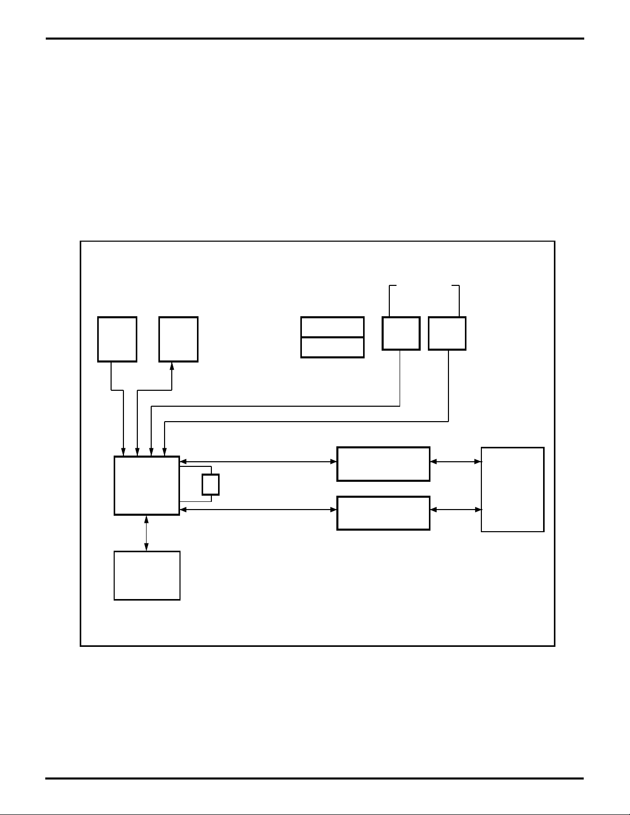
The Z80185/195 Development Kit (Z8018500ZCO) provides all the necessary hardware, software,
and documentation to properly evaluate and begin design development using the Z80185/195 Smart
Peripheral Controller. The kit includes a monitor program shipped in EPROM and a software monitor
program (TZ.EXE) that runs on a PC. The monitor program enables you to do the following: download
and run programs from a PC—with or without breakpoints, display and fill memory locations, compare
contents of memory, and read/write from the I/O Ports. The kit also comes with P1284 IEEE Centronics
and ASCI UART device drivers and some working sample codes. A full schematic of the board is also
included in this manual.
The Z80185/195 Development Kit is carefully engineered to provide the best balance between
reasonable cost and useful features to shorten your development time for products using the Z80185/
195 (see Figure 1-1 for Functional Block Diagram). The Z80185/195 Development Board is an
excellent hardware example of how to design with the Z80185/195 Smart Peripheral Controller.
KEY FEATURES OF THE Z80185/195 DEVELOPMENT KIT
■ Complete Start-Up Kit Capabilities for Developers.
■ Provides Hands-On Access to the Z80185/195 Smart Peripheral Controller.
■ Serves as a Developmental Platform for Trial Implementation of a Specific Application.
■ Configured to Operate as a Standalone Unit.
■ Includes All Necessary Cabling for Power Supply Connection.
SUPPORTED ZILOG DEVICES
Device Packaging
Z80185/195 100-Pin QFP
UM951800100
1-1
Page 6
ZILOG
Z80185/195 DEVELOPMENT KIT
USER'S MANUAL
HARDWARE SPECIFICATIONS
Dimensions 8.8 in. H x 5.9 in W
Oscillator Frequency (OSC) 18.432 MHz
Host Interface RS-232 (EIA-232) or RS-422 (EIA-530) Serial Link
Serial Baud Rate 115,200 bps (RS-232); Up to OSC/64 (RS-422/485)
Power Supply Voltage +5 VDC ±5%
Power Supply Current Less than 1A
Operating Temperature 20 degrees C, ±10 degrees C
Operating Humidity 10-90% RH (non-condensing)
Push Button
ROM
512K
Z80185/
Z80195
Parallel
Connectors (3)
RAM
128K
18.432
MHz
Power/GND
Connectors (2)
Drivers and Receivers
Drivers and Receivers
Reset NMI
RS-232
Serial
Connectors (6)
RS-422
Figure 1-1. Z80185/195 Development Kit
Functional Block Diagram
1-2 UM951800100
Page 7

ZILOG
Z80185/195 DEVELOPMENT KIT
USER'S MANUAL
SUPPORT PRODUCTS PACKAGE CONTENTS
Hardware
Zilog Z80185 Evaluation Board, including:
Z80195 Smart Peripheral Controller
EPROM (Contains Debug Monitor)
128Kx8 25ns RAM
RS-232 Line Drivers and Receivers
RS-422 Line Drivers and Receivers
(5) EIA-570 DB-25 Connectors (for the three serial ports: ASCI0, ASCI1, and EMSCC)
DIN-8 LocalTalk Connector
Standard DB-25 Parallel Port Connector
Standard 36-Pin “Centronics” Connector
Miniaturized 36-Pin Connector (recommended for new designs by IEEE P1284 specifications.)
Berg Headers (surrounding the Z80185/195 location for all the CPU signals)
NMI and Reset Buttons
Power Cable with Banana Plugs
Software
Z80185 Sample Files and Monitor Source Diskette
ZASM-Cross Assembler Diskette/MOBJ-Object Utility Diskette
Device Drivers Diskette
Description of Z80185 Sample Files and Monitor Source Diskette
MAKE.BAT Assembly Macro
FIXLSTG.EXE Listing-Fixer Executable
TZ.EXE Terminal Emulator Executable
185MACRO.LIB Z80185 Assembler Macros
185MON.HEX Z80185 Debug Monitor (Intel hex format)
185MON.S Z80185 Debug Monitor Source
DISTEST.HEX Test for Monitor Disassembly (Intel hex format)
DISTEST.S Test for Monitor Disassembly Source
FVT0.HEX Z80185 ASCI0 FVT (Intel hex format)
FVT0.S Z80185 ASCI0 FVT Source
FVT1.HEX Z80185 ASCI1 FVT (Intel hex format)
FVT1.S Z80185 ASCI1 FVT Source
HOST.HEX Z80185 Host FVT (Intel hex format)
HOST.S Z80185 Host FVT Source
PERIF.HEX Z80185 Peripheral FVT (Intel hex format)
PERIF.S Z80185 Peripheral FVT Source
TSTRST20.HEX Test Program for Monitor Services (Intel hex format)
TSTRST20.S Test Program for Monitor Services Source
TZ96COM1.PIF Windows Startup File for TZ on COM1
TZ96COM2.PIF Windows Startup File for TZ on COM2
Publications
Z80185/195 Development Kit User's Manual
asm S800, Z800 Cross Assembler User's Guide
UM951800100
Zilog Universal Object File Utilities User's Guide
Z80185/195 Software Dev. Kit User's Manual
1-3
Page 8

ZILOG
Z80185/195 DEVELOPMENT KIT
USER'S MANUAL
REQUIREMENTS AND RESTRICTIONS
Minimum Hardware
The Z80185/195 Development Board can be used with a dumb terminal and a power supply;
however, a PC is recommended to take full advantage of the development kit's software downloading
and development capabilities.
If Using a PC
Any IBM PC (or 100-percent compatible) that can run MS-DOS V.5.0. We recommend an IBM PC (or
100-percent compatible) 386-based machine at 20 MHz with 4 MB RAM, hard disk drive (with 1 MB
available), and a 3.5 floppy disk drive (see "Notes" that follow).
Minimum Software Operating Systems
MS-DOS V.5.0 (see "Notes" that follow)
Additional Items Not Supplied with the Support Package
A source of power (+5 VDC ±10%) can be used in place of the PC. This can be a laboratory power
supply with supply current of 1.0A.
Notes:
1. Debug Monitor with a Dumb Terminal. Two Debug Monitor commands (“L” for loading a hex file
and “N” for changing the Serial Data Rate) will not properly function when running on a dumb terminal
(refer to Chapter 3: Using the Debug Monitor, “TZ Program Restrictions”).
2. TZ Terminal Emulation Program. The TZ Program, which is included on the Z80185 Sample
Files and Monitor Source Diskette, was developed to run with MS-DOS V.5.0; however, the program
may run on earlier versions. One (or more) copies of the TZ Program will run under Windows 3.1 (and
also may run under earlier versions). The kit includes .PIF files on the Z80185 Sample Files and
Monitor Source Diskette to help start the TZ program in the Windows environment.
3. PC Models/Serial Baud Rates. The maximum serial rate that can be used between a PC and the
development kit board is dependent upon which PC model and configuration that is used. If the baud
rate is too fast for the PC, characters will be lost during lengthy display sequences initiated by the
monitor program D, U, or F commands. Also, downloading may fail if the serial rate is too high.
General Guidelines:
PC Configuration Maximum Baud Rate (bps)
286 or 386 (slower) 19,200
386 (faster), 486, Pentium 57,600
486 (faster) and later generation 115,200
machines with serial drivers and
receivers rated for higher baud rates.
1-4 UM951800100
Page 9

ZILOG
U
SER'S MANUAL
Z80185/195 DEVELOPMENT KIT
USER'S MANUAL
CHAPTER 2
S
ETUP AND INSTALLATION
INTRODUCTION
This chapter describes the various steps necessary to start development using the Z80185/195
evaluation board. The sections covered in this chapter are as follows:
■ Installing the Software
■ Setting Up the Hardware
– Serial Channels
– Parallel Channel
– Other Jumper Options
■ Connecting to Power
■ Initial Checkout/Sample Session
INSTALLING THE SOFT WARE
Software for the Z80185/195 Development Kit is stored on two diskettes:
1. Z80185 Sample Files and Monitor Source Code Diskette
2. Zilog ZASM Cross Assembler/Zilog MOBJ Object File Util. diskette
Z80185 Source Diskette Installation
1. Select the “Run” command from the “File” menu under Microsoft Windows “Program Manager”.
2. Insert the diskette labeled “Z80185 Sample Files and Monitor Source” into drive A (or drive B, if
appropriate).
3. Type “a:\setup” and press ENTER. (Type “b:setup” if drive B is used.)
A dialog box will now prompt you for the directory into which the software will be installed (default
is C:\185). The setup program will copy the files into the target directory, creating an icon in the
Windows environment. After the installation is finished, you can move the icon into any program
group of your choice.
Note: The icon will be created in the window that is currently selected.
4. Remove diskette and store in a safe place when done.
UM951800100
2-1
Page 10

ZILOG
Z80185/195 DEVELOPMENT KIT
USER'S MANUAL
INSTALLING THE SOFTWARE (Continued)
Creating TZ Program (TZ.EXE) Icon Using Windows Program Manager
This kit includes a software monitor program that runs on a PC. If you choose to create a TZ icon from
which you can run the TZ program, perform the following steps:
1. Select “New” from the Program Manager’s “File” menu and select “OK” or press ENTER on the
keyboard.
2. Type the designated name (such as “tz 9600 com1”) in the Program Manager window.
3. Type the full path and filename of (one of) the .PIF files you copied from the 185 Source Diskette,
such as “C:\WINDOWS\TZ96COM1.PIF”.
4. Type the full path of the directory you created (such as “C:\185”), then press ENTER.
The program item icon should then be created and ready to use. If you want to run copies of TZ on
both COM1 and COM2, repeat Steps 1–4.
Notes:
1. Modification of the “win.ini”, “autoexec.bat”, or “config.sys” files is not required.
2. Consult MS-Windows documentation if you need additional information about alternate install
procedures.
3. Refer to the README files on diskettes. (The README files are easily accessed via the Microsoft
Windows "Notepad" program.)
ZASM-Cross Assembler/MOBJ-Object Utility Installation (Optional)
If you are using the ZASM Cross Assembler/MOBJ-Object File Utility, install the appropriate diskette
before installing the GUI diskette. (You may choose to use a different assembler.)
1. Select the "Run" command from the "File" menu under Microsoft Windows "Program Manager".
2. Insert the diskette labeled "Zilog ZASM Cross Assembler/Zilog MOBJ Object File Util." into drive
A (or drive B, if appropriate).
3. Type "a:\setup" and press ENTER. (Type "b:setup" if drive B is used.)
A screen now appears listing various installation options.
4. Select the desired installation option ("Full Installation" is the default selection; however, only Z8
installation is required.)
5. Press ENTER and follow on-screen instructions.
6. Remove diskette and store in a safe place when done.
Note: The installation procedure can be run before creating the installation directory.
2-2
UM951800100
Page 11

ZILOG
Z80185/195 DEVELOPMENT KIT
USER'S MANUAL
SETTING UP THE SERIAL CHANNELS
The Z80185/195 includes three serial channels called ASCI0, ASCI1, and the ESCC channel. The
board is shipped ready to use ASCI1 as the user interface for the Debug Monitor, with RS-232 DCE
pinning on ASCI1 connector J9.
Using the ASCI1 User Interface (Default). If you will be using ASCI1, and you don’t need to configure
ASCI0 or the ESCC channel, perform the following steps:
1. Connect a DB-9 to DB-25 serial cable between one of the COM ports of your PC and J9 on the
board.
2. Skip to the “Setting Up the Parallel Channel” section, which follows.
Otherwise, read the applicable sections that follow.
Selecting the Serial Channel for the Monitor
The Debug Monitor in the EPROM on the board can use ASCI0, ASCI1, or the ESCC channel for its
user interface. On this 185/195 board, this choice is controlled by jumpers on J14-2 and J14-5, which
are connected to the 185’s /INT1 and /INT2 pins respectively. You will want to connect a DB-9 to DB25 serial cable between a COM port of your PC and the female DB-25 DCE connector for the selected
channel.
Function Jumper Connections
ASCI1 for the Monitor interface J14-2 and J14-5 open, connect the serial cable to J9.
ASCI0 for the Monitor interface Ground J14-2, J14-5 open, connect the serial cable to
J13.
ESCC channel for the Monitor J14-2 open, ground J14-5, connect the serial cable
interface to J11.
Ground pins to J14-2 or J14-5 J8-6, J10-7, J12-7, J15-4, J15-6, and the following pins
around the Z80195 processor:
Pin Connector Pin
18 P2-20
40 P3-10
59 P4-22
63 P4-18
92 P5-9
ESCC LocalTalk/AppleTalk on J16
Pins 1-3 of J15 determine whether the ESCC channel takes its receive data from the LocalTalk/
AppleTalk connector J16, or one of the DB25 connectors J10 or J11.
UM951800100
2-3
Page 12

ZILOG
Z80185/195 DEVELOPMENT KIT
USER'S MANUAL
SET TING UP THE HARDWARE (Continued)
Function Jumper Connections
LocalTalk/AppleTalk connector J15-1 to J15-2
from J16
J10 or J11 J15-2 to J15-3
Note: This board has no provision for “clock” or “handshake” input or output on the J16 LocalTalk/
AppleTalk connector.
RS-232 or RS-422/485 for ASCI0 and ESCC Channel
Pins 4-7 of J15 determine whether the board uses RS-232 “unbalanced” signaling, or RS-422/485
“balanced” or “differential” signaling on the DB-25 connectors for ASCI0 and the ESCC channel. RS232 is more common but is limited up to 115,200 bits/second, and cables up to about 25 feet long.
RS-422/485 can handle higher serial rates and longer cables.
Function Jumper Connections
RS-232 for ESCC on J10 or J11 Leave open J15-5.
RS-422/485 on J10 or J11 Jumper J15-4 to J15-4.
RS-232 for ASCI0 on J12 or J13 Leave open J15-7 open.
RS-422/485 on J12 or J13 Jumper J15-7 to J15-6 to use.
DCE or DTE Pinning for ASCI0 and the ESCC Channel
The RS-232 and EIA-570 standards define connection between a piece of Data Terminal Equipment
(DTE) such as a dumb terminal or a computer system, and a piece of Data Communications
Equipment (DCE) such as a modem. The 185/195 board can act as either a DTE or DCE device. For
ASCI0 and the ESCC channel this choice depends on which connector you use.
Male DB-25 J10. Provides DTE pinning for the ESCC channel, and is suitable for connecting to a
modem via a “straight-through” cable, or to a computer via a “null modem” cable.
Female DB-25 J11. Provides DCE pinning for the ESCC channel, and is suitable for connecting to
a computer via a straight through cable, or to a modem via a null modem cable.
Male DB-25 J12. Provides DTE pinning for ASCI0, and is suitable for connecting to a modem via a
straight-through cable, or to a computer via a null modem cable.
Female DB-25 J13. Provides DCE pinning for ASCI0, and is suitable for connecting to a computer
via a straight-through cable, or to a modem via a null modem” cable.
Note: Signal names, which are shown on the board schematic in this manual with an over bar to
indicate an active low signal, are shown in the following sections with a slash before the name, for
example “/DSR”.
2-4
UM951800100
Page 13

ZILOG
Z80185/195 DEVELOPMENT KIT
USER'S MANUAL
ESCC DTE Pinning on J10
Since the ESCC channel signals on the Z80185 are named appropriately for the DTE role, the
following signals on J10 are driven from (or received into) the pins of the same name on the ESCC
channel: TxD, RxD, RTS, CTS, DCD, DTR, and RxC.
DSR on J10 is received onto J14-8 (/DSR on the schematic). It can be jumpered to the 185’s PIA15
pin on J14-7, or PIA14 on J14-9.
TxC (DCE source) on J10 is received onto J7-1 (/TXCI on the schematic). It can be jumpered to ESCC
/TRXC on J7-2, in which case /TRXC should be programmed as an input.
The signal on J7-3 (/TXCO on the schematic) drives TxC (DTE source) on J10. It can be jumpered
from ESCC /TRXC on J7-2, in which case /TRXC should be programmed as an output.
ESCC DCE Pinning on J11
The ESCC signals on the Z80185 are named appropriately for the DTE role, so the connections on
J11 are backward:
The ESCC TxD output drives RxD on J11.
The ESCC RxD input is taken from TxD on J11.
The ESCC RTS output drives CTS on J11.
The ESCC CTS input is taken from RTS on J11.
The ESCC DTR output drives DSR on J11.
DTR on J11 is received onto J14-8 (/DSR on the schematic). It can be jumpered to the 185’s PIA15
pin on J14-7, or PIA14 on J14-9.
The signal on J14-10 (/DCDO on the schematic) drives DCD on J11. It can be jumpered from the 185’s
PIA14 pin on J14-9, or PIA12 on J14-11.
The ESCC RTXC input is taken from TxC (DTE source) on J11.
The signal on J7-3 (/TXCO on the schematic) drives both RxC and TxC (DCE source) on J11. It can
be jumpered from ESCC TRXC on J7-2.
UM951800100
2-5
Page 14

ZILOG
Z80185/195 DEVELOPMENT KIT
USER'S MANUAL
SET TING UP THE HARDWARE (Continued)
ASCI0 DTE Pinning on J12
TXA0 drives TxD on J12.
RxD on J12 is received into RXA0.
/RTS0 drives RTS on J12
CTS on J12 is received onto J7-10 (/CTS0 on the schematic). It can be jumpered to the 185’s
/CTS0/RxS pin on J7-9, in which case this pin should be programmed for the /CTS0 function.
The signal on J14-12 (/DTR0 on the schematic) drives DTR on J12. It can be jumpered from the
185’s PIA13 pin on J14-11, or PIA12 on J14-13.
DSR on J12 is received onto J14-14 (/DSR0 on the schematic). It can be jumpered to the 185’s
PIA12 pin on J14-13, or PIA11 on J14-15.
DCD on J12 is received onto J7-8 (/DCD0I on the schematic). It can be jumpered to the 185’s
/DCD0/CKA1 pin on J7-7, in which case this pin should be programmed for the /DCD0 function. A
pull-up resistor is included on DCD from J12 so that it will appear asserted if the remote system doesn’t
drive DCD, as required by ASCI0.
RxC on J12 is received onto J7-4 (CK0I on the schematic). It can be jumpered to the 185’s CKA0/
CKS pin on J7-5, in which case this pin should be programmed for the CKA0 function, and CKA0
should be programmed as a 1X clock input.
The signal on J7-6 (CKOO on the schematic) drives TxC (DTE source) on J12. It can be jumpered
from the 185’s CKA0/CKS pin on J7-5, in which case this pin should be programmed for the CKA0
function and CKA0 should be programmed as a 1X clock output.
ASCI0 DCE Pinning on J13
The ASCI0 signals on the Z80185 are named appropriately for the DTE role, so the connections on
J13 are backward:
The ASCI0 TXA0 output drives RxD on J13.
The ASCI0 RXA0 input is taken from TxD on J13.
The ASCI0 RTS0 output drives CTS on J13.
The ASCI0 CTS0 input is taken from RTS on J13.
The signal on J14-12 (/DTR0 on the schematic) drives DSR on J13. It can be jumpered from the
185’s PIA13 pin on J14-11, or PIA12 on J14-13.
2-6
UM951800100
Page 15

ZILOG
Z80185/195 DEVELOPMENT KIT
USER'S MANUAL
ASCI0 DCE Pinning on J13 (Continued)
DTR on J13 is received onto J14-14 (/DSR0 on the schematic). It can be jumpered to the 185’s
PIA12 pin on J14-13, or PIA11 on J14-15.
The signal on J14-16 (/DCD0O on the schematic) drives DCD on J13. It can be jumpered from the
185’s PIA11 pin on J14-15, or PIA10 on J14-17.
The signal on J7-6 (CK0O on the schematic) drives both RxC and TxC (DCE source) on J13. It
can be jumpered from the 185’s CKA0/CKS pin on J7-5, in which case the pin should be programmed
for the CKA0 function, and CKA0 should be programmed as a 1X clock output. In this case, ASCI0
will be able to receive data correctly only if the remote transmitter actually uses TxC (DCE source)
to clock data onto TxD.
TxC (DTE source) on J13 is received onto J7-4 (CK0I on the schematic). It can be jumpered to
the 185’s CKA0/CKS pin on J7-5, in which case the pin should be programmed for the CKA0 function,
and CKA0 should be programmed as a 1X clock input.
No signal on J13 is received to the 185’s /DCD0/CKA1 pin, which is connected to J7-7. A pullup resistor, on the DCD0 receivers used with J12, ensures that the signal at J7-8 will be asserted Low,
as required for ASCI0 reception if J7-7 is jumpered to J7-8 and software programs /DCD0/CKA1 for
the /DCD0 function.
ASCI1 and J9
Only one connector is provided for ASCI1, the DB-25 female J9. It includes only transmit and receive
data, no “modem control” or status signals. The jumper header J8 controls both the pinning of J9 (DTE
versus DCE) and the signaling type (RS-232 versus differential):
Function Jumper Connections
RS-232 DCE pinning J8-4 to J8-6, J8-7 to J8-8, and J8-9 to J8-10
RS-232 DTE pinning J8-4 to J8-6, J8-7 to J8-9, and J8-8 to J8-10.
Differential DCE pinning J8-1 to J8-2, J8-3 to J8-4, J8-7 to J8-8. and J8-9 to J8-10.
For differential DTE pinning J8-1 to J8-3, J8-2 to J8-4, J8-7 to J8-9, and J8-8 to J8-10.
Differential receiving is compatible with RS-422 and RS-485. For ASCI1 and J9, differential
transmission differs from RS-422 and RS-485 in that it uses ±5V swings. This is because it uses part
of the 26LS30 driver U17 that is used for LocalTalk/ AppleTalk on J16. However, this differential output
is compatible with most differential receivers as long as they can tolerate a voltage differential up to
10V without damage.
UM951800100
2-7
Page 16

ZILOG
Z80185/195 DEVELOPMENT KIT
USER'S MANUAL
SETTING UP THE PARALLEL CHANNEL (Optional)
(Skip this section if you are not using the 185’s parallel port.)
Host
If you are using the 185 board to act as a Host on the parallel port, such as connecting it to a printer,
make sure there is a shunt block on J5 and not on J6.
Peripheral
If you are using the 185 board to act as a Peripheral on its parallel port, such as connecting it to a
the parallel port of a PC, make sure there is a shunt block on J6 and not on J5.
Notes:
1. The shunt block on J5 or J6 configures serial resistors on outputs and pull-up resistors on inputs,
among the nine parallel control signals: nAck, Busy, PError, Select, nFault, nAutoFd, nStrobe,
nSelectIn, and nInit. The shunt block also controls the state of the PERIPHI signal on the J3 and
J4 connectors, and of the HOSTHI signal on J4.
PERIPHI and HOSTHI are also connected to J14-6 and J14-3 respectively, from which one of them
can be connected to a 185 input such as PIA16 or PIA15, so that software on the 185 can sense
which shunt block is installed and set the mode of the parallel port to Host or Peripheral
accordingly. If you have software that provides such automatic mode setting, consult its
documentation for the proper jumper setting.
2. You can also fill the J5 or J6 jumper block (but not both) with individual shunts.
3. Connect your parallel cable to one of J2, J3, or J4. The DB-25 J2 is typically used if you want the
board to act as a Host using a traditional parallel cable. The full-size 36-pin “Centronics”
connector J3 is typically used if you want the board to act as a Peripheral using a traditional parallel
cable. The half-size 36-pin connector J4 is recommended by the 1284 draft for new Host and
Peripheral designs.
OTHER JUMPER OPTIONS
EPROM Size
J1 should be set according to the size of the EPROM installed in the U2 socket:
Jumper J1-1 to J1-2 for 27256 (or smaller) EPROM
Jumper J1-2 to J1-3 for 27512 EPROM
2-8
UM951800100
Page 17

ZILOG
Z80185/195 DEVELOPMENT KIT
USER'S MANUAL
Summary of J14
The following lists all the signals in the J14 header, many of which are provided for applicationdependent.
Pin Signal Function
J14-1 Z80185 /INT0 Ext. interrupt requests
J14-2 Z80185 /INT1 Ext. interrupt requests and/or monitor console selection
J14-3 J4 HOSTHI Auto-adaptation host versus peripheral
J14-4 Z80185 PIA16
J14-5 Z80185 /INT2 Ext. interrupt requests and/or monitor console selection
J14-6 J3,4 PERIPHI Auto-adaptation host versus peripheral
J14-7 Z80185 PIA15
J14-8 J10 DSR or J11 DTR Input not provided by ESCC
J14-9 Z80185 PIA14
J14-10 J11 DCD Out Output not provided by ESCC
J14-11 Z80185 PIA13
J14-12 J12 DTR or J13 DSR Output not provided by ASCI0
J14-13 Z80185 PIA12
J14-14 J12 DSR or J13 DTR Input not provided by ASCI0
J14-15 Z80185 PIA11
J14-16 J13 DCD Out Output not provided by ASCI0
J14-17 Z80185 PIA10
UM951800100
2-9
Page 18

ZILOG
Z80185/195 DEVELOPMENT KIT
USER'S MANUAL
CONNECTING TO A POWER SUPPLY
Connecting to a separate power supply. If your power supply allows voltage adjustment, do the
following (refer to Figure 2-1):
1. Turn the 2.0A power supply on and adjust it to +5V.
2. Set the +5V power supply for at least 1.5A, if there’s a current-limiting adjustment.
3. Turn the supplies off, or make sure non-adjustable supplies are off.
4. Locate the short power cable (red wire, black wire, and banana plugs on one end).
5. Insert one end of the power cable (polarized) into P1 of the board.
6. Plug the black banana plug into the black jack on the power supply connector that’s labeled COM,
GND, or with a ground symbol.
7. Plug the red plugs into the proper red jacks on the power supply (labeled "+" or "+V" or "+5V").
Note: Some manufacturers will also have black or white jacks. Refer to individual manufacturers'
manuals to decide how to connect in this case.
Using your PC for power supply. Most PCs have extra power capacity to allow for add-in cards. You
may be able to connect a spare disk-drive power cable to P1, thus eliminating the need for a separate
power supply.
Note: The board draws less than 1A on +5V and does not use the +12V in the disk-drive cable.
1. Turn the 2.0A power supply on and adjust it to +5V.
2. Set the +5V power supply for at least 1.5A, if there’s a current-limiting adjustment.
3. Turn the supplies off, or make sure non-adjustable supplies are off.
4. Locate the short power cable (red wire, black wire, and banana plugs on one end).
5. Insert one end of the power cable (polarized) into P1 of the board.
Connecting the Serial Cable to the PC. Locate the serial cable. Connect the male end to the female
connector on the side of the development board, and the female end to either the COM1, COM2,
COM3, or COM4 connector of your PC.
Note: If connector availability is limited to a 9-pin COM1 through COM4, you’ll have to use either a
different cable or a 25-pin to 9-pin converter. (Zilog does not provide either of these items.)
2-10
Figure 2-1. Z80185/195 Development Board-to-PC Hook-Up Diagram
UM951800100
Page 19

ZILOG
Z80185/195 DEVELOPMENT KIT
USER'S MANUAL
INITIAL CHECKOUT/SAMPLE SESSION
The sections that follow are designed to provide an initial checkout of the hardware/software
installation and setup and introduce you to some of the features of the TZ terminal emulation program.
1. If necessary, power-up the PC and wait for the boot process to complete.
2. Double-click the TZ icon (if you have installed the TZ Program as an icon within Windows Program
Manager).
or
At the DOS prompt (in the directory containing TZ.EXE, DISTEST.HEX, and TSTRST20.HEX), type
“TZ COM
cable), then press ENTER.
3. Power-up the system.
If powering up the board from a separate power supply:
Set the voltage to +5V.
n
” (where n is the number of the COM port to which you connected the Monitor serial
If powering up the board from your PC:
Type “V” at your keyboard.
4. Type “H” (for Help) at a Monitor command prompt to see a list of commands.
5. Type an “L”. The screen should show “Enter File Name:”
Note: Only if using the TZ emulation program only. Not available if you are using a dumb terminal
or running a PC communications program other than TZ.
6. Type “DISTEST”, then press ENTER. You should see an incrementing count. Its final value should
be followed with the message “Intel hex lines—Done” and a new Monitor command prompt:
“Z80185>”
Note: Refer to Chapter 3: “Using the Debug Monitor” if you do not get the “hex done” message.
7. Type a “U”. The screen should display the following message: “Disassemble Starting At (just
CR = from PC):”
Press ENTER to indicate that you want to disassemble from the current Program Counter value,
which was set to the start of the DISTEST program as it was downloaded.
The screen should now show a new prompt “Number of Instructions:”
8. Type “16”, then press ENTER.
A screen full of assembly-language instructions should appear, followed by another commandline prompt.
UM951800100
2-11
Page 20

ZILOG
Z80185/195 DEVELOPMENT KIT
USER'S MANUAL
9. Press ENTER at the command prompt to disassemble more of the instructions in DISTEST.
Note: The file, which preceded, is not intended to be an executable program. Rather, it is the test
file for the disassembly command in this Debug Monitor. DISTEST includes all the instructions
that can be executed by the Z8018x family processors.
10. Type another “L” at the command prompt, then type “TSTRST20” as the file name, followed
pressing ENTER.
11. Again you should see the final count followed by the “ Intel hex lines—Done” and a Monitor
command prompt.
12. Type “G” at the monitor command prompt. The screen should show the message “Go Starting
at Address:”. Press ENTER to start the TSTRST20 program.
Note: Chapter 3 describes the I/O services that the Debug Monitor provides to downloaded
programs.
The first two lines displayed by TSTRST20 tests the ‘message’ service, and should appear as:
(message) Test RST 20 services (date)
A. Enter a hex value up to 4 digits (in_hl)
B. Enter a 1- to 4-digit hex value followed by pressing ENTER. This tests the ‘in_hl’ service. The
following display tests three services called ‘out_hl’, ‘out_a’, and ‘out_char’, and should appear
as follows:
16-bit value we saw (out_hl) :
XXXX
the terminating character was (out_a) : 0D
and the ‘any digits’ CC was (out_char) : NZ
Waiting for you (test_char) :
XXXX
C. Check that the value shown above as
is the hex value you entered.
D. Type any data character on the keyboard. This tests two services called ‘test_char’ and
‘in_char’.
After you type a character, the concluding messages from TSTRST20 should appear as
follows:
Your character was (in_char) : XX
A F B C D E H L A’ F’ B’ C’ D’ E’ H’ L’ I IX IY SP EI 75 00 03 00 01 0D 82 6A 00 00 00
00 00 00 00 00 00 0000 0000 0000 0 814C EF RST 28
Z80185>
XX
13. Check whether the value shown as
in the preceding paragraph is the hex value of the
character entered. The second through fourth lines above indicate that the TSTRST20 program
ended with a Breakpoint instruction.
This completes the Initial Checkout/Sample Session.
2-12
UM951800100
Page 21

ZILOG
U
SER'S MANUAL
Z80185/195 DEVELOPMENT KIT
USER'S MANUAL
CHAPTER 3
U
SING THE MONITOR PROGRAM
INTRODUCTION
This chapter begins by describing the Debug Monitor program, followed by the simple procedures
necessary to start and stop the program. This chapter concludes with the full descriptions of each
of the available Program Commands and RST 20H Services. This chapter is sectionalized as follows:
■ About the Monitor Program
■ Getting Started
■ Program Commands
■ RST 20H Services
About the Monitor Program
The Z80185/195 Board includes a Debug Monitor program in its EPROM chip (U2). The Z80185
monitor program can be used with a character-oriented dumb terminal; however, terminal emulation
facilities are available on a PC when the TZ.EXE program is used. The TZ program on the PC allows
you to do the following: download a PC program, run a PC program (with or without breakpoints),
display/fill memory locations, compare memory contents, display/modify registers, and read/write
from/to I/O ports, including Z80185/195 SPC Registers.
Two hex files, DISTEST.HEX and TSTRST20.HEX, containing binary/absolute programs for the
Z80195 processor are provided with this development kit. You can use the Zilog Z800 assembler and
object utilities provided with this kit, or third-party Z80 or Z180 software development tools to generate
your own 185/195 programs and hex files.
Monitor Code
The Debug Monitor, which resides in the EPROM shipped on the board, occupies about 6K bytes of
code starting at address 00000. Whenever you power-up the board or press the RESET button, the
Debug Monitor takes control and sets the ROM/RAM boundary to hex 02000, so in effect it takes up
the first 8K bytes of the Z80185 address space. (For more information, refer to Chapter 4: Reference,
"Debug Monitor Memory Map" section.)
UM951800100
3-1
Page 22

ZILOG
GETTING STARTED
Starting Up the TZ Program
(in DOS or at DOS Prompt in Windows)
Z80185/195 DEVELOPMENT KIT
USER'S MANUAL
Note: Proper installation of the monitor program assumes that the proper
hardware setup
is complete.
Before loading the monitor program, refer to "Chapter 2: Setup and Installation" for the complete
procedure for hardware setup, including setting up jumpers, connecting cables, and applying power
to the Z80185/195 Development Board.
1. Ensure that the PC is powered up and is functioning properly.
2. Verify that all jumper settings and cable connections are correct.
3. If using a PC, load the Z80185 Source diskette and copy the TZ.EXE program to the PC.
n
4. Enter "TZ com
" (where n is the COM serial port number [1–4] of choice); press <RETURN>.
5. Connect the power supply cable to the 185/195 board.
6. Apply power through connector P1 on the 185/195 board.
7. Press the RESET button (S1).
Starting Up the TZ Program
(TZ Icon in Windows)
Note: Proper installation of the monitor program assumes that the proper
hardware setup
is complete.
Before loading the monitor program, refer to "Chapter 2: Setup and Installation" for the complete
procedure for hardware setup, including setting up jumpers, connecting cables, and applying power
to the Z80185/195 Development Board.
1. Ensure that the PC is powered up and is functioning properly.
2. Verify that all jumper settings and cable connections are correct.
3. Double-click on the TZ icon (specifying one of the COM serial ports).
4. Connect the power supply cable to the 185/195 board.
5. Apply power through connector P1 on the 185/195 board.
6. Press the RESET button (S1).
Opening Screen Message
If all connections to your PC are correct, you should see the following opening message at power up
or by pressing the RESET button on the board:
1
Zilog Z80185 Monitor Version
v.m
Z80185 >
1
Where v is the current version of the debug monitor and m is the revision.
Exiting the TZ Program
If the TZ Program was started with DOS, type Control–C. TZ will return you to the DOS prompt.
If the TZ Program was started in Windows by double-clicking the TZ icon, the window will close or the
full-screen display will be replaced by the Windows environment.
3-2
UM951800100
Page 23

ZILOG
Z80185/195 DEVELOPMENT KIT
USER'S MANUAL
TZ Program Restrictions
If the Debug Monitor is used with a dumb terminal, or with a PC running a terminal emulator other than
TZ, two commands will not work as described in this chapter:
1. An “L” command (for loading a hex file) will not be followed by the “Enter File Name:” prompt.
2. An “N” command (changing the serial data rate) will either show nonsense characters, or no
characters at all, after you type the speed-selection digit.
Monitor Debug Program and Serial Baud Rates
If you use an N command to change the baud rate between the board and the PC, both the TZ
Program on the PC and the Debug Monitor on the board change the rate simultaneously. Quitting,
starting, or pressing RESET on the board always sets the rate used by the Monitor to 9600 bps.
However, you can start TZ at any of the baud rates available by using the N command.
n
Type the baud rate after the COM
(where n is the COM serial port number [1–4]) argument in a DOS
command, as in the following example:
TZ COM2 57600
This third argument (as in "57000" in the preceding example) can be any of the following entrees:
1200, 2400, 4800, 9600, 14400, 19200, 28800, 38400, 57600, or 115200.
115,200 bps does not work well on many PCs and may not be offered in the Debug Monitor’s prompt
for the N command. (Refer to the following guidelines for PC configurations/baud-rate selection.)
PC Models/Serial Baud Rates
The maximum serial rate that can be used between a PC and the development kit board is dependent
upon which PC model and configuration that is used. If the baud rate is too fast for the PC, characters
will be lost during lengthy display sequences initiated by the monitor program D, U, or F commands.
Also, downloading may fail if the serial rate is too high.
PC Configuration Maximum Baud Rate (bps)
286 or 386 (slower) 19,200
386 (faster), 486, Pentium 57,600
486 (faster) and later generation 115,200
machines with serial drivers and
receivers rated for higher baud rates.
Note: Under Windows, you can use the Windows .PIF editor to make a new PIF file that includes such
a command line, and then use a File/New command under the Program Manager to make a new icon
that references the new .PIF file.
UM951800100
3-3
Page 24

ZILOG
Z80185/195 DEVELOPMENT KIT
USER'S MANUAL
PROGRAM COMMANDS
Program Basics
1. The monitor program will prompt for all commands (A–X) with “Z80185 >”.
2. Press the <ESC> key if you make a mistake or want to return to the command prompt.
3. An audible signal is given if the monitor doesn’t recognize a command.
4. Numerical values are expected to be in hex. If you don’t type a value (but just press <RETURN>),
a zero value is assumed, except in the editing modes of the “A” and “E” commands.
5. Many commands (A, C, D, E, F, G, I, M, R, S, T, and U, for example) are repeatable from where
they left off, by pressing <RETURN> at the command prompt.
6. When you type the first letter of the command the monitor will automatically type in the rest of the
prompt.
7. To exit the program (and DOS), Type "<CTRL C>".
8. The monitor program is not case sensitive.
Table 3-1. Program Command Reference Chart
Command Description Page No.
A Alter Memory 3-3
B Set or Show Breakpoints 3-3
C Compare Memory Data 3-4
D Display Memory Data 3-4
E Edit/Display I/0 Data 3-5
F Fill Memory 3-6
G Go To Program 3-6
H Help 3-7
I Input Data from I/O Address 3-7
K Kill Breakpoint(s) 3-7
L Load an Intel Hex File 3-8
M Move Memory to Memory 3-8
N Change Serial Data Rate 3-9
O Output Byte to I/O Address 3-9
R Display/Alter Registers 3-10
S Step (Over Subroutine Calls) 3-11
T Step (Into Subroutine Calls) 3-11
U Disassemble Instructions 3-12
V Display Version of the Program 3-12
X EXamine the MMU 3-13
3-4
UM951800100
Page 25

ZILOG
Z80185/195 DEVELOPMENT KIT
USER'S MANUAL
Alter Memory [A]
Use the Alter Memory command to modify bytes in memory. The display shows the address and
current data. When a byte is entered, it is written to the address shown, and the next higher or lower
address is displayed. The monitor program does not write to the location when entering a terminating
value without the hex value before it. Terminating is as follows:
<ESC> Does not store a preceding value and returns to the command prompt.
. Stores a preceding value if any and returns to the command prompt.
= Stores a preceding value if any, stays at the same location, re-reads and re-
displays.
CR,tab,Space,+,> Stores a preceding value if any, and go to the next location.
-,<,^ Stores a preceding value if any, and go to previous location.
Example:
Z80185 >Alter Memory starting at: 8000
8000 39 : bb
8001 20 : aa
8002 FF : ^
8001 AA : <ESC>
Z80185 >
Set or Show Breakpoints [B]
A break point is a special status you can associate with a memory address in RAM, so that when you
set a program running with a Go-To-Program G command, and the execution comes to that address
at the start of the instruction, it will stop running and return to the monitor command prompt. Up to eight
(8) breakpoints can be set at one time. The code at each break address is replaced with the RST 28H
(hex EF). This opcode will bring the control back to the monitor if execution reaches the breakpoint.
The user can code RST 28H instruction right into the program, at the end of the program, and/or at
any point the user needs the control to come back to the monitor. In the case of this “hard-coded”
RST 28H, the monitor program simply increments the address to the following instruction before it
starts execution. If a breakpoint is set at the starting address in a G command, the monitor program
will set one single-steps over the first instruction, then sets all the breakpoints and goes. The monitor
also checks to see whether a requested breakpoint is in fact in RAM (where it must be).
Note: Breakpoints must be set at the first byte of an instruction. (Instruction starting points can be
determined by doing a command U.) Breakpoints that are randomly set (or breakpoints that are set
in the middle of an instruction) may cause faulty operation of the instruction.
(Example of the "Set or Show Breakpoints" command is shown on the next page.)
UM951800100
3-5
Page 26

ZILOG
Z80185/195 DEVELOPMENT KIT
Set or Show Breakpoints [B] (Continued)
Example:
Z80185 > Breakpoint at Address (just CR to Display All): 2100
Z80185 > Breakpoint at Address (just CR to Display All):
Breakpoints 2100
Z80185 >
Z80185 > Go Starting at Address : 9000
A F B C D E H L A’ F’ B’ C’ D’ E’ H’ L’ I IX IY SP EI
FF FF FF FF FF FF FF FF FF FF FF FF FF FF FF FF 00 FF FF FF FF 2000 0
2042 F7 RST 30
Z80185>
Compare Memory Data [C]
USER'S MANUAL
This command compares a specified number of memory bytes and displays the differences.
Example:
Z80185 > Compare Memory Data Starting at: 0000
with Memory Data Starting at: 8000
Number of Bytes: 3
0000 = 00 : 8000 = 39
0001 = F5 : 8001 = 88
0002 = ED : 8002 = 00
Z80185 >
Display Memory Data [D]
Displays memory bytes in hex and ASCII format. The display can be paused by entering
"^S (CTRL+S)". Entering another "^S" while paused displays one more line. Any other key quits the
pause. The <ESC> key stops the display after the current line has been printed. If the <ENTER> key
is entered at the command prompt after a D command, then the monitor will display the same number
of bytes again, starting at the address after the last one is displayed.
Example:
Z80185 > Display Memory Starting at: 0000
Number of Bytes : 5
0000 00 F5 ED 57 F3 ...w.
Z80185 >
3-6
UM951800100
Page 27

ZILOG
Z80185/195 DEVELOPMENT KIT
USER'S MANUAL
Edit/Display I/O Data [E]
This command allows editing or display of registers in I/O space. First, the program asks for a starting
address, which can be 16 bits. Then it asks for the number of registers to display. If you enter "0" or
just a <RETURN>, you enter Editing mode. If you enter a nonzero value, that number of I/O registers
will be displayed following the starting address.
Example of Display Mode:
Z80185 > Edit/Display Starting at I/O Register: 40
Display How Many Bytes (just CR to Edit): 10
0040 78 78 78 78 78 78 78 78 78 78 78 78 78 78 78 78
Z80185>
In Editing mode, the program displays what it reads from each I/O location. Entering a hex value
followed by a valid terminating character (not including <ESC>) will make the program write the
entered value to the location. The program recognizes the following terminating characters:
<ESC> Does not store a preceding value and returns to the command prompt.
. Stores a preceding value if any and returns to the command prompt.
= Stores a preceding value if any, stays at the same location, re-reads and re-
displays.
CR,tab,Space,+,> Stores a preceding value if any, and go to the next location.
-,<,^ Stores a preceding value if any, and go to previous location.
In addition to these, a backspace character after a hex character “unenters” one hex character.
With the original Z80 Family, I/O addresses were 8-bit wide and thus I/O space was 256 bytes long.
In the Z180 Family (this monitor program), I/O addresses are treated as 16-bits wide, thus I/O space
contains 65,536 bytes. The Z180 peripherals appear only on the first 256-byte page, in addressees
0000 -003F unless they have been reallocated by software to 0040-007F or 0080-00BF. The unique
peripherals of the Z80185/195 may appear in every page or only the first page depending on a
programmable bit in the I/O register.
UM951800100
3-7
Page 28

ZILOG
Z80185/195 DEVELOPMENT KIT
USER'S MANUAL
Fill Memory [F]
This commands fills memory with a specified byte value. The desired numbers of bytes can be up
to 65K.
Be careful with overwriting monitors RAM variables, which are typically at addresses 2000-20FF.
Example:
Z80185>Fill Memory starting at: 8000
With data: 77
Number of Bytes: 3
Z80185>Display Memory Starting at: 8000
Number of Bytes : 3
8000 77 77 77 www
Z80185>
Caution: RAM locations 2000-20FF are used by the monitor program as workspace. F, M, and L
commands should not be used within this memory range.
Go to Program [G]
This command transfers Z80185 execution from the monitor program to user code. If an address is
supplied, it is used as the users PC for execution. If no address is supplied, the value that was stored
in the PC register is used as the starting address. The PC register is initialized to 2100 hex. Before
the monitor sets the user program into execution, it proceeds as follows:
1. Checks to see if the opcode at the starting address is a hard-coded RST 28H. If so, it advances
the starting address over the RST 28H and proceeds to Step 3.
2. If not, it checks for a breakpoint at the starting address. If so, it invokes an implicit T command,
to single step over the first instruction, returning to Step 3 when this has been completed.
3. For each breakpoint, it saves the opcode at that address in a RAM table and substitutes the
opcode RST 28H (EF).
4. It stacks the starting address and restores all the user register values that were saved in the last
RESET, breakpoint, hard-coded RST 28, or NMI, and may have modified since then.
5. It enables or disables interrupts per the saved EI value.
6. It uses a RET instruction to begin execution at the starting address stacked in Step 4.
After a G command, there are several ways that control can return to the monitor: if execution comes
to an RST 28 instruction, either due to a breakpoint or hard-coded one, if execution comes to an illegal
instruction, or when pressing the NMI or RESET buttons. In all the above cases the monitor saves the
register contents and program counter and restores the opcodes of any breakpoints that were set.
Then it displays the register contents, program counter, and (for NMI or an illegal instruction) a
message why execution stopped.
Example: Z80185> Go Starting at Address :
3-8
UM951800100
Page 29

ZILOG
Help [H]
Entering “H” displays the command set available from the monitor program.
A – Alter Memory
B – Set or Show Breakpoints
C – Compare Memory Data
D – Display Memory Data
E – Edit/Display I/O Data
F – Fill Memory
G – Go to Program
H – Help
I – Input Data from I/O Address
K – Kill Breakpoint(s)
L – Loading an Intel Hex Code
M – Move Memory to Memory
N – Change Serial Data Rate
O – Output Byte to I/O Address
R – Display/Alter Registers
S – Step (Over Subroutine CALLs)
T – Step (Into Subroutine CALLs)
U – Disassemble Instructions
V – Display Version of the Monitor
X – EXamine the MMU
Z80185/195 DEVELOPMENT KIT
USER'S MANUAL
Input Data from I/O Address [I]
This performs an 8-bit input from a 16-bit I/O address.
Example:
Z80185>Input From I/O Address : c0
00C0 78
Z80185>
Kill Breakpoint(s) [K]
If the user enters a breakpoint value (the monitor program will check to see if it is a valid breakpoint)
in hex the monitor will kill that breakpoint. A <CR> will kill all the breakpoints that are set.
Example:
Z80185> Kill Breakpoint at address (do <CR> for all) :
UM951800100
3-9
Page 30

ZILOG
Z80185/195 DEVELOPMENT KIT
USER'S MANUAL
Loading an Intel Hex File [L]
This command affects both the Z80185 monitor and the TZ.EXE program, which runs on a PC. After
you enter the name of the file, the PC sends it to the board RAM. This command and the N command
are the two commands that require that you use the TZ.EXE program on a PC as the terminal.
Example:
Z80185> File name: at.hex
78 Intel hex lines—done
Z80185>
Move Memory to Memory [M]
This command moves a specified number of bytes from one address to another. In order to handle
overlapping "from" and "to" areas correctly, the monitor moves data differently, depending on how the
addresses compare. If the "from" address is greater than the "to" address, the monitor moves the data
between the starting address and higher addresses thereafter. If the "from" address is less than the
"to" address, the monitor begins moving between the highest addresses implied by the number of
bytes and lower address thereafter until it gets down to the starting address entered.
Example:
Z80185>Move From Memory starting at: 2020
to Memory starting at: 2020
Number of Bytes: 4
Z80185>
Caution: RAM locations 2000–20FF are used by the monitor as workspace. F, M, and L commands
should not be used within this memory range.
3-10
UM951800100
Page 31

ZILOG
Z80185/195 DEVELOPMENT KIT
USER'S MANUAL
Change Serial Data Rate [N]
Changes the bit rate of serial communications between the host and the board. This command and
the L command are the two commands that require that you use the TZ.EXE program on a PC as the
terminal. These values are OSC dependent.
Caution: Do not change the oscillator on board.
Example:
Z80185>Enter 0 for 1200 Bits/Second
1 for 2400
2 for 4800
3 for 9600
4 for 14400
5 for 19600
6 for 28800
7 for 38400
8 for 57600
Enter 9 for 115200 bits/second: 9
Z80185>
Output Byte to I/O Address [O]
This performs an 8-bit output to a 16-bit I/O address.
Example:
Z80185>Output to I/O Address : c3
Data: 00
Z80185>
UM951800100
3-11
Page 32

ZILOG
Z80185/195 DEVELOPMENT KIT
USER'S MANUAL
Display/Alter Registers [R]
You will be asked for a starting register. If no register name is supplied, all CPU registers are
displayed. If a register name is supplied, display starts from that register, and the values can be
modified.
<ESC> Does not store a preceding value and returns to the command prompt.
. Stores a preceding value if any and returns to the command prompt.
= Stores a preceding value if any, stays at the same location, re-reads and re-
displays.
CR,tab,Space,+,> Stores a preceding value if any, and go to the next location.
-,<,^ Stores a preceding value if any, and go to previous location.
Example:
Z80185 > Display/Alter Register (just CR Displays All) :
A F B C D E H L A’ F’ B’ C ’ D’ E’ H’ L’ I IX IY SP EI
02 00 0F 04 00 00 20 A7 FE 80 00 00 00 00 00 00 00 021B 0000 205E 0
OFDD CB7F BIT 7,A
Step (Over Subrouting Calls) [S]
This command steps a specified number of instructions, stepping “over” subroutine calls and RST.
In this command, monitor stores an EF opcode after the instruction, so that it will get control back after
the subroutine has complete execution and returns.
If no value is entered, then “1” step is assumed. If the user enters more than two hex digits, only the
LS 2 hex digits are used, so the maximum number of instructions that can be step by one command
is 255 (decimal). For each instruction step over, the monitor will display the register values, the
Program Counter, and the instruction in both hex and disassembled format. The instructions to be
stepped over must be in RAM. The monitor accomplishes stepping by placing the opcode (EF) RST
28H after each instruction, and/or for instruction, by placing the EF opcode at the destination. It then
restores the registers and transfers control to the single instruction, being assured of getting control
right back because of the RST 20s. Simple operations (such as unconditional JR, JP, and RET) are
handled by updating the user PC without storing any RST 28s. RST instructions can only be “stepped
over” with an “S” command, because they transfer the control into ROM. A hard-coded RST 28 is
treated as a No-Op while stepping. The monitor advances the program counter to the next instruction.
The RST 28s are not placed at breakpoints while stepping.
Example:
Z80185 > Step How Many Instructions:
3-12
UM951800100
Page 33

ZILOG
Z80185/195 DEVELOPMENT KIT
USER'S MANUAL
Step (Into Subroutine Calls) [T]
This command steps a specified number of instructions, stepping “into” the subroutines and calls.
Stepping can be done in RAM and the monitor program checks for this. You can step “over” but not
“into” an RST or ROM-based subroutines. The monitor program stores an EF at the start of the
subroutine. If the user steps into a HALT or SLP instruction and no device interrupts occur to escape
this state, the user must press the NMI key to keep stepping.
Example:
Z80185 > Step How Many Instructions:
Disassemble Instructions [U]
This command disassembles a specified number of instructions from a specified starting address.
The next instruction is always disassembled whenever the registers are shown the following: R
command with no operand, breakpoint, step, and NMI. The maximum value for this command is in
the range hex 15-17 (decimal 21-23) since more that this will not fit on the screen. After disassembling
the indicated number of instructions, the monitor returns to the command prompt. If you respond with
a <RETURN> only, the monitor disassembles the same number of instructions again, starting from
where it left off. This facility is useful for “scanning through” a program looking for a particular type
of code.
Example:
Z80185>Disassemble starting at (just CR = From PC):9000
Number of Instructions: 2
9000 39 ADD HL,SP
9001 2039 JR NZ,903C
Z80185>
UM951800100
3-13
Page 34

ZILOG
Z80185/195 DEVELOPMENT KIT
USER'S MANUAL
Display Version of the Monitor [V]
Entering a "V" displays the software version number
Example:
Z80185 > Version
Zilog Z8015 Monitor Version 1.2
Z80185>
Examine the MMU [X]
This command can be used to control the mapping from logical to physical memory. When you enter
an "X" at a command prompt, the monitor program reads the values in the three MMU registers (CBAR,
BBR, and CBR) and translates their values into to the “current MMU map” that it displays on the next
five lines. Next, it displays two lines describing the contents of the CBAR register, displays its
contents, and allows you to enter a new value for CBAR. After that, if the CBAR value enables/uses
the Bank area, the monitor program similarly describes BBR, displays its value, and allows you to
enter a new value for it. Finally, it describes CBR, displays its value, and allows you to enter a new
value.
If you don’t enter a new value for any of the three registers, the monitor program will return to the
command prompt after you enter <RETURN> for CBR. Otherwise it will write the new value(s) at this
point and will attempt to go back and re-display the new MMU map as before.
If you selected a combination of register values that doesn’t let the monitor program keep running,
you will not see the new MMU map. Trial and error is the easiest route to working with the MMU using
this command.
Example:
Z80185>eXamine the MMU
Current MMU Map:
Area Logical Address Range Physical Address Range
Common 0 (Not Used)
Bank 0000-EFFF 00000-0EFFF
Common 1 F000-FFFF 0F000-0FFFF
CBAR MS 4 = Boundary between Bank and Common 1 Areas in Logical Address Space
CBAR LS 4 = Boundary between Common 0 and Bank Areas in Logical Address Space
CBAR F0 :
BBR contains adder to Bank Area Logical Address to get Physical Address
BBR 00 :
CBR contains adder to Common 1 Area Logical Address to get Physical Address
CBR 00 :
Z80185>
3-14
UM951800100
Page 35

ZILOG
Z80185/195 DEVELOPMENT KIT
USER'S MANUAL
Other Features
NMI
If you press the NMI button, you will see the following message:
Non-Maskable Interrupt!
A F B C D E H L A’ F’ B’ C’ D’ E’ H’ L’ I IX IY SP EI
FC 7C 00 00 81 53 00 BF 62 04 01 0E 90 00 80 89 00 904A 800F 827A 0
0F77 CB7F BIT 7,A
Z80185 >>
Trap
The Z80185/195 family of products has a feature to cause a “Trap” when an undefined instruction is
executed. If this occurs, you will see the following message:
Undefined instruction Trap!
A F B C D E H L A’ F’ B’ C’ D’ E’ H’ L’ I IX IY SP PC
XX XX XX XX XX XX XX XX XX XX XX XX XX XX XX XX XX XX XX XXX XX
Z80185 >
UM951800100
3-15
Page 36

ZILOG
Z80185/195 DEVELOPMENT KIT
USER'S MANUAL
RST 20H Services
The monitor program offers a number of console I/O services using the RST 20 instruction. These
services have advantages over direct I/O to the ASCI or ESCC registers—they implicitly use the
console port that the user has selected.
Prior to the RST 20h, the user should set the B register to identify the services required, from the
following list. No registers are changed except as indicated.
The TSTRST20. HEX program, which is on the Z80185 Source Diskette, can be used to test the RST
20 instruction.
(B) Name Service Performed
0 out_char Waits, if necessary, for monitor console device to be ready for output,
then outputs the ASCII character in A. A is not changed.
1 in_char Waits, if necessary, for user to press a key on the monitor console
device; returns its ASCII value in A.
2 test_char Returns NZ condition code if user has pressed a key on the monitor
console device, else returns Z. A is not changed.
3 out_a Waits, if necessary, for monitor console device to be ready for output,
then outputs the 8-bit hexadecimal value in A. A is changed.
4 out_hl Waits, if necessary, for monitor console device to be ready for outputs,
then outputs the 16-bit value in HL. A is changed.
5 in_hl Waits for user to enter a hexadecimal value on the monitor console
device, and returns it in HL. Terminating characters are as in monitor
hex entry; the terminating character is returned in A.
6 message Outputs a null-terminated string—pointed to by HL—on the monitor
console device. HL is advanced over the terminating null. A is not
changed.
3-16
UM951800100
Page 37

ZILOG
Z80185/195 DEVELOPMENT KIT
USER'S MANUAL
USER'S MANUAL
CHAPTER 4
REFERENCE
MEMORY CONFIGURATIONS AND JUMPER SETTINGS
Memory Configurations
EPROM. The Z80185/195 board is shipped with a 28-pin ROM socket. The board is being shipped
with populated 27256-type ROM, which contains the Z80185 monitor program.
SRAM. The Z80185/195 board is shipped with 128Kx8 25ns RAM.
Pin
Jumper Numbers Description
J1 2-3 2751 Type
J1 1-2 27256 Type (or smaller)
Parallel Interface—IEEE 1284 Centronics Interface
Jumper Description
J2 Standard DB-25 parallel port connector as on PCs.
J3 Standard 36-pin “Centronics” connector found on printers.
J4 Miniaturized 36-pin (IEEE P1284-recommended for new
designs).
Host Operation
Jumper Description
J5 Place the supplied jumper blocks across all pins of J5.
J6 Empty
Peripheral Operation
Jumper Description
J6 Place the supplied jumper blocks across all pins of J6.
J5 Empty
UM951800100
4-1
Page 38

ZILOG
Z80185/195 DEVELOPMENT KIT
USER'S MANUAL
Serial Interface
The serial I/O pins of the Z80185/195 serial controller are connected to the J9–J13 connector blocks
through RS-232 or RS-422 drivers and receivers. J9–J12 are EIA-570 DB-25 connectors for the three
serial ports (ASCI0, ASCI1, and EMSCC) of the Z80185/195.
Jumper Description
J9 ASCI1, data (TXD and RXD) only, female, DTE or DCE
pinning.
J10 EMSCC, male DTE pinning.
J11 EMSCC, female DCE pinning.
J12 ASCI0, male DTE pinning.
J13 ASCI0, female DCE pinning.
The following option jumpers are associated with the above ports:
Pin
Jumper Numbers Description
J15 2–3 Insert jumper to use J10 or J11 rather than J16 with the
ESCC.
J15 4–5 Insert jumper to use RS-422 signaling on J10 and J10.
Remove to use RS-232.
J15 6–7 Insert jumper to use RS-422 signaling on J12 and J13.
Remove to use RS-232.
To use J9 as RS-232 DTE:
Pin
Jumper Numbers
J8 4–6, 7–9, 8–10
To use J9 as RS-232 DCE:
Pin
Jumper Numbers
J8 4–6, 7–8, 9–10
4-2
UM951800100
Page 39

ZILOG
Serial Interface Jumper Settings (Continued)
To use J9 as RS-422 DTE:
Pin
Jumper Numbers
J8 1–3, 2–4, 7–9, 8–10
To use J9 as RS-422 DCE:
Pin
Jumper Numbers
J8 1–2, 3–4, 7–8, 9–10
ESCC Signals
Z80185/195 DEVELOPMENT KIT
USER'S MANUAL
To use the ESCC /TRXC pin as an input from J10:
Pin
Jumper Numbers
J7 1–2
To use the ESCC /TRXC pin as an output on J10 or J11:
Pin
Jumper Numbers
J7 2–3
LocalTalk Connector
J16 is a LocalTalk
Apple Macintosh
®
connector for the ESCC. This 8-pin circular DIN connector is compatible with
®
Plus and later models of the Macintosh computer, and with other AppleTalk®/
LocalTalk equipment.
Pin
Jumper Numbers
J15 1–2
UM951800100
4-3
Page 40

ZILOG
Z80185/195 DEVELOPMENT KIT
USER'S MANUAL
Serial Interface Jumper Settings (Continued)
ASCI0 Signals
Pin
Jumper Numbers Description
J7 4–5 To use ASCI0 CKA0 as an input from J12 or J13.
J7 5–6 To use ASCI0 CKA0 as an output on J12 or J13.
Modem Control Signals
J14 allows jumpering between modem control inputs and outputs for J10-13 as shown below.
Pin
Jumper Numbers Description
J14 8 “DSR” input from J10 or “DTR” input from J11.
J14 10 “DCD” output to J11.
J14 12 “DTR” output to J12 or “DCR” output to J13.
J14 14 “DSR” input from J12 or “DTR” input from J13. J14-16 is
“DCD” output to J13.
4-4
UM951800100
Page 41

ZILOG
Z80185/195 DEVELOPMENT KIT
USER'S MANUAL
Other Jumpering
The following modem control signals can be interconnected with PIA16-10 I/Os on the Z80185/195
or INT0-2 inputs on the Z80185/195 and the HOSTHI and PERIPHI lines of J3 and J4, using the J14
jumper block as follows.
Pin
Jumper Numbers Description
J14 1 INT0
J14 2 INT1
J14 3 HOSTHI (J4)
J14 4 PIA16
J14 5 INT2
J14 6 PERIPHI (J3, J4)
J14 7 PIA15
J14 8 ESCC DxR in
J14 9 PIA14
J14 10 ESCC DCD out
J14 11 PIA13
J14 12 ASCI0 DxR out
J14 13 PIA12
J14 14 ASCI0 DxR in
J14 15 PIA11
J14 16 ASCI0 DCD out
J14 17 PIA10
UM951800100
4-5
Page 42

ZILOG
Z80185/195 DEVELOPMENT KIT
USER'S MANUAL
Debug Monitor Memory Map
The Debug Monitor sets the ROM/RAM boundary to hex 02000, so in effect it takes up the first 8K bytes
of the Z80185 address space. Since there is 128K bytes of RAM on the board, the Debug Monitor
sets the top of RAM to 21FFF. The latter 72K bytes of this RAM can only be accessed by using the
Z80185’s Memory Management Unit (MMU).
The Debug Monitor also uses the first 256 bytes of RAM, addresses 02000-020FF, for its variables,
stacks, and tables. When you apply power to the board or press RESET, the user Stack Pointer (SP)
is set to 00000, so that the first stack locations used will be 0FFFE and 0FFFF, and the Monitor sets
its user Program Counter value (PC) to 02100. 02100 is the suggested starting address for programs
downloaded and run under the Debug Monitor. Higher starting addresses are acceptable.
ContentsMemory Address
00000
. . .
01A??
Debug Monitor (ROM)
. . .
01FFF
02000
. . .
020FF
02100 (PC after RESET)
. . .
. . .
0FFFF (STACK after RESET)
10000
. . .
. . .
21FFF
22000
. . .
FFFFF
Figure 3-1. Debug Program Memory Map
Reserved (ROM)
Monitor RAM
User RAM
(Accessible without MMU)
User RAM
(Accessible via MMU)
No Memory
4-6
UM951800100
Page 43

ZILOG
Z80185/195 DEVELOPMENT BOARD SCHEMATIC
Board schematic not available at this site.
Z80185/195 DEVELOPMENT KIT
USER'S MANUAL
UM951800100
4-7
Page 44

ZILOG
U
SER'S MANUAL
Z80185/195 DEVELOPMENT KIT
USER'S MANUAL
APPENDIX A
D
RIVERS OVERVIEW
Introduction
The Z80185/195 Development Kit includes device drivers software that supports the serial or P1284
Centronics ports. The software is structured as modular libraries so that you can use only those pieces
actually needed. A brief description of the software follows. (Refer to the Z80185/195 Device Drivers
User's User's Manual, which is included in this kit.)
ASCI UART Driver
The ASCI UART serial driver supports the new, higher bit rates of the Z80185/195’s enhanced ASCI
serial port as well as the improved parity and data width features, which provides a high-speed serial
interface to the system. It supports the port either on a character-by-character basis or with the use
of a DMA channel. In addition, it supports the following standard RS-232 flow control protocols:
■ XON/XOFF
■ CTS/RTS
P1284 Centronics Drivers
The P1284 driver uses the Z80185/195’s P1284 hardware to implement either the host or printer side
of this emerging IEEE standard. It deals with all of the signaling required to change from one mode
to a different mode within the P1284. The characteristics of the P1284 drivers can be summarized as
follows.
UM951800100
A-1
Page 45

Z80185/195 DEVELOPMENT KIT
ZILOG
USER'S MANUAL
OVERVIEW (Continued)
P1284 Key Features
■ There are separate drivers for inclusion in printers (peripheral) and the host computer.
■ Both drivers support compatible, byte, nibble, and ECP modes.
■ Both drivers achieve high data rates by using the hardware support of the Z80185/195 for data
transfer. In most cases, performance will be limited by the "other end" of the P1284 cable.
■ P1284 mode used by the P1284 host driver is determined by software—when you open the 1284
printer driver, it will use any of the supported modes that the attached host requests.
■ When your software requests to transmit data, each driver will do all the signaling necessary to
set the P1284 connection to the outgoing direction and send the data.
■ When no data is available to be transmitted, each driver will "listen" for incoming data and send
it to your application.
■ The printer software can specify the device ID, and the P1284 printer driver will send it to the host
automatically whenever it is requested.
■ The host software can request the device ID of the attached printer, and the P1284 host driver
will fetch it.
Performance
In ECP mode, the burst transfer speed is limited only by the speed of the DMA channel and the speed
of the station at the other end of the 1284 connection. Two Z80185/195s operating at 18.432 MHz can
communicate in ECP mode at approximately 1.4 MBytes/sec., and even faster for higher clock rates.
In compatibility mode, the burst transfer speed is limited by the pulse widths required by the P1284
standards; two Z80185/195’s can achieve approximately 0.7 MBytes/sec. in this mode.
A-2
UM951800100
Page 46

ZILOG
U
SER'S MANUAL
Z86295 DEVELOPMENT KIT
USER'S MANUAL
APPENDIX B
A
CCESSING THE
ZILOG BULLETIN BOARD INFORMATION
The Zilog Bulletin Board Service (ZBBS) currently provides basic information on Zilog products and
includes a ROM CODE upload area. In addition, the ZBBS provides valuable information on items of
interest, such as Zilog specialty software and documentation.
How to Access the ZBBS
The ZBBS can be reached by dialing 1-408-370-8024. The ZBBS supports speeds up to 28.8K
Baud with connections 8-N-1. (We recommend that you use an ANSI/BBS terminal emulation
setup.)
ZBBS/I
NTERNET
To preview information or download files, follow the on-screen instructions.
ZILOG ON THE INTERNET
Zilog has a Home Page on the Internet. The Home Page address is:
http://www.zilog.com
UM951800100
B-1
Page 47

Z8® CCP™ EMULATOR
ZILOG
U
SER'S MANUAL
USER'S MANUAL
APPENDIX C
PROBLEM / SUGGESTION REPORT FORM
If you experience any problems while operating this product, or if you note any inaccuracies while
reading the User's Manual, please copy this form, fill it out, then mail or fax it to Zilog (see "Return
Information"). We also welcome your suggestions!
Customer Information
Name ___________________________________
Company _______________________________
Address ________________________________
City/State/ZIP ____________________________
Country _____________________________________
Telephone _________________________________
Fax Number ________________________________
E-Mail Address _____________________________
Product Information
ICEBOX Serial # or Board Fab #/Rev. #________________
Software Version ___________________________________
User's Manual Number (on back cover) _______________
Host Computer Description/Type _____________________
___________________________________________________
Problem Description or Suggestion
Provide a complete description of the problem or your suggestion. If you are reporting a specific
problem, include all steps leading up to the occurrence of the problem.
Return Information
Zilog, Inc.
Support Products Director, D2–3
210 E. Hacienda Ave.
Campbell, CA 95008-6600
Fax Number: 408-370-8056
UM951800100
C-1
 Loading...