

Page 1

Z8018x
Family MPU
User Manual
UM005003-0703
ZiLOG WORLDWIDE HEADQUARTERS • 532 Race Street • SAN JOSE, CA 95126-3432
T
ELEPHONE: 408.558.8500 • FAX: 408.558.8300 • WWW.ZILOG.COM
Page 2

Z8018x
Family MPU User Manual
This publication is subject to replacement by a later edition. To determine whether a later edition
exists, or to request copies of publications, contact
ZiLOG Worldwide Headquarters
532 Race Street
San Jose, CA 95126-3432
Telephone: 408.558.8500
Fax: 408.558.8300
www.ZiLOG.com
Windows is a registered trademark of Microsoft Corporation.
Document Disclaimer
© 2003 by ZiLOG, Inc. All rights reserved. Information in this publication concerning the devices,
applications, or technology described is intended to suggest possible uses and may be superseded. ZiLOG,
INC. DOES NOT ASSUME LIABILITY FOR OR PROVIDE A REPRESENTATION OF ACCURACY OF
THE INFORMATION, DEVICES, OR TECHNOLOGY DESCRIBED IN THIS DOCUMENT. ZiLOG
ALSO DOES NOT ASSUME LIABILITY FOR INTELLECTUAL PROPERTY INFRINGEMENT
RELATED IN ANY MANNER TO USE OF INFORMATION, DEVICES, OR TECHNOLOGY
DESCRIBED HEREIN OR OTHERWISE. Except with the express written approval ZiLOG, use of
information, devices, or technology as critical components of life support systems is not authorized. No
licenses or other rights are conveyed, implicitly or otherwise, by this document under any intellectual property
rights.
UM005003-0703
Page 3

MANUAL OBJECTIVES
This user manual describes the features of the Z8018x MPUs.This manual
provides basic programming information for the Z80180/Z8S180/
Z8L180. These cores and base peripheral sets are used in a large family of
ZiLOG products. Below is a list of ZiLOG products that use this class of
processor, along with the associated processor family. This document is
also the core user manual for the following products:
Part Family
Z80180 Z80180
Z8S180 Z8S180
Z8L180 Z8L180
Z8018x
Family MPU User Manual
iii
Z80181 Z80180
Z80182 Z80180, Z8S180*
Z80S183 Z8S180
Z80185/195 Z8S180
Z80189 Z8S180
* Part number-dependant
Intended Audience
This manual is written for those who program the Z8018x.
Manual Organization
The Z8018x User Manual is divided into five sections, seven appendices,
and an index.
UM005003-0703
Page 4

Z8018x
Family MPU User Manual
iv
Sections
Z8018X MPU Operation
Presents features, a general description, pins descriptions, block
diagrams, registers, and details of operating modes for the Z8018x MPUs.
Software Architecture
Provides instruction sets and CPU registers for the Z8018x MPUs.
DC Characteristics
Presents the DC parameters and absolute maximum ratings for the
Z8X180 MPUs.
AC Characteristics
Presents the AC parameters for the Z8018x MPUs.
Timing Diagrams
Contains timing diagrams and standard test conditions for the Z8018x
MPUs.
Appendices
The appendixes in this manual provide additional information applicable
to the Z8018x family of ZiLOG MPUs:
•
Instruction set
•
Instruction summary table
•
Op Code map
•
Bus Control signal conditions in each machine cycle and interrupt
conditions
•
Operating mode summary
•
Status signals
•
I/O registers and ordering information
UM005003-0703
Page 5

Z8018x
Family MPU User Manual
Table of Contents
Z80180, Z8S180, Z8L180 MPU Operation . . . . . . . . . . . . . . . . . . . .1
Features . . . . . . . . . . . . . . . . . . . . . . . . . . . . . . . . . . . . . . . . . . . . . . . . . . .1
General Description . . . . . . . . . . . . . . . . . . . . . . . . . . . . . . . . . . . . . . . . .1
Pin Description . . . . . . . . . . . . . . . . . . . . . . . . . . . . . . . . . . . . . . . . . . . . .7
Architecture . . . . . . . . . . . . . . . . . . . . . . . . . . . . . . . . . . . . . . . . . . . . . .12
Operation Modes . . . . . . . . . . . . . . . . . . . . . . . . . . . . . . . . . . . . . . . . . .15
CPU Timing . . . . . . . . . . . . . . . . . . . . . . . . . . . . . . . . . . . . . . . . . . .18
Wait State Generator . . . . . . . . . . . . . . . . . . . . . . . . . . . . . . . . . . . .27
HALT and Low Power Operation Modes
(Z80180-Class Processors Only) . . . . . . . . . . . . . . . . . . . . . . . .31
Low Power Modes
(Z8S180/Z8L180 only) . . . . . . . . . . . . . . . . . . . . . . . . . . . . . . .36
Add-On Features . . . . . . . . . . . . . . . . . . . . . . . . . . . . . . . . . . . . . . .36
STANDBY Mode . . . . . . . . . . . . . . . . . . . . . . . . . . . . . . . . . . . . . . .37
STANDBY Mode Exit wiht BUS REQUEST . . . . . . . . . . . . . . . . .38
STANDBY Mode EXit with External Interrupts . . . . . . . . . . . . . . .39
IDLE Mode . . . . . . . . . . . . . . . . . . . . . . . . . . . . . . . . . . . . . . . . . . . 40
STANDBY-QUICK RECOVERY Mode . . . . . . . . . . . . . . . . . . . .41
Internal I/O Registers . . . . . . . . . . . . . . . . . . . . . . . . . . . . . . . . . . . .41
MMU Register Description . . . . . . . . . . . . . . . . . . . . . . . . . . . . . . .60
Interrupts . . . . . . . . . . . . . . . . . . . . . . . . . . . . . . . . . . . . . . . . . . . . .65
Interrupt Acknowledge Cycle Timings . . . . . . . . . . . . . . . . . . . . . .82
Interrupt Sources During RESET . . . . . . . . . . . . . . . . . . . . . . . . . . .83
Dynamic RAM Refresh Control . . . . . . . . . . . . . . . . . . . . . . . . . . .86
DMA Controller (DMAC) . . . . . . . . . . . . . . . . . . . . . . . . . . . . . . . .90
Asynchronous Serial Communication Interface (ASCI) . . . . . . . .115
v
UM005003-0703
Page 6

Z8018x
Family MPU User Manual
vi
Baud Rate Generator
(Z8S180/Z8L180-Class Processors Only) . . . . . . . . . . . . . . . 143
Clocked Serial I/O Port (CSI/O) . . . . . . . . . . . . . . . . . . . . . . . . . . 146
CSI/O Registers Description . . . . . . . . . . . . . . . . . . . . . . . . . . . . . 147
Programmable Reload Timer (PRT) . . . . . . . . . . . . . . . . . . . . . . . 156
Miscellaneous . . . . . . . . . . . . . . . . . . . . . . . . . . . . . . . . . . . . . . . . 172
Software Architecture . . . . . . . . . . . . . . . . . . . . . . . . . . . . . . . . . . 173
Instruction Set . . . . . . . . . . . . . . . . . . . . . . . . . . . . . . . . . . . . . . . . . . . 173
CPU Registers . . . . . . . . . . . . . . . . . . . . . . . . . . . . . . . . . . . . . . . . . . . 175
DC Characteristics . . . . . . . . . . . . . . . . . . . . . . . . . . . . . . . . . . . . . 185
Absolute Maximum Rating . . . . . . . . . . . . . . . . . . . . . . . . . . . . . . . . . 185
Z80180 DC Characteristics . . . . . . . . . . . . . . . . . . . . . . . . . . . . . . . . . 186
Z8S180 DC Characteristics . . . . . . . . . . . . . . . . . . . . . . . . . . . . . . . . . 187
Z8L180 DC Characteristics . . . . . . . . . . . . . . . . . . . . . . . . . . . . . . . . . 189
AC Characteristics . . . . . . . . . . . . . . . . . . . . . . . . . . . . . . . . . . . . . 193
AC Characteristics—Z8S180 . . . . . . . . . . . . . . . . . . . . . . . . . . . . . . . 193
Timing Diagrams . . . . . . . . . . . . . . . . . . . . . . . . . . . . . . . . . . . . . . 197
Standard Test Conditions . . . . . . . . . . . . . . . . . . . . . . . . . . . . . . . . . . 205
Instruction Set . . . . . . . . . . . . . . . . . . . . . . . . . . . . . . . . . . . . . . . . 207
Register . . . . . . . . . . . . . . . . . . . . . . . . . . . . . . . . . . . . . . . . . . . . . . . . 207
Bit . . . . . . . . . . . . . . . . . . . . . . . . . . . . . . . . . . . . . . . . . . . . . . . . . . . . 207
Condition . . . . . . . . . . . . . . . . . . . . . . . . . . . . . . . . . . . . . . . . . . . . . . . 208
Restart Address . . . . . . . . . . . . . . . . . . . . . . . . . . . . . . . . . . . . . . . . . . 209
UM005003-0703
Page 7

Z8018x
Family MPU User Manual
Flag . . . . . . . . . . . . . . . . . . . . . . . . . . . . . . . . . . . . . . . . . . . . . . . . . . . .209
Miscellaneous . . . . . . . . . . . . . . . . . . . . . . . . . . . . . . . . . . . . . . . . . . . .210
Data Manipulation Instructions . . . . . . . . . . . . . . . . . . . . . . . . . . . . . .211
Data Transfer Instructions . . . . . . . . . . . . . . . . . . . . . . . . . . . . . . . . . .222
Program and Control Instructions . . . . . . . . . . . . . . . . . . . . . . . . . . . . .229
Special Control Instructions . . . . . . . . . . . . . . . . . . . . . . . . . . . . . .235
Instruction Summary . . . . . . . . . . . . . . . . . . . . . . . . . . . . . . . . . . .237
Op Code Map . . . . . . . . . . . . . . . . . . . . . . . . . . . . . . . . . . . . . . . . . .247
Bus Control Signal Conditions . . . . . . . . . . . . . . . . . . . . . . . . . . . .251
Bus and Control Signal Condition in each Machine Cycle . . . . . . . . .251
vii
Interrupts . . . . . . . . . . . . . . . . . . . . . . . . . . . . . . . . . . . . . . . . . . . . . . . .279
Operating Modes Summary . . . . . . . . . . . . . . . . . . . . . . . . . . . . . .281
Request Acceptances in Each Operating Mode . . . . . . . . . . . . . . . . . .281
Request Priority . . . . . . . . . . . . . . . . . . . . . . . . . . . . . . . . . . . . . . . . . .282
Operation Mode Transition . . . . . . . . . . . . . . . . . . . . . . . . . . . . . . . . . .283
Other Operation Mode Transitions . . . . . . . . . . . . . . . . . . . . . . . . . . . .285
Status Signals . . . . . . . . . . . . . . . . . . . . . . . . . . . . . . . . . . . . . . . . .287
Pin Outputs in Each Operating Mode . . . . . . . . . . . . . . . . . . . . . . . . . .287
Pin Status . . . . . . . . . . . . . . . . . . . . . . . . . . . . . . . . . . . . . . . . . . . . . . .288
I/O Registers . . . . . . . . . . . . . . . . . . . . . . . . . . . . . . . . . . . . . . . . . .293
Internal I/O Registers . . . . . . . . . . . . . . . . . . . . . . . . . . . . . . . . . . . . . .293
Ordering Information . . . . . . . . . . . . . . . . . . . . . . . . . . . . . . . . . . . . . .303
UM005003-0703
Page 8

Z8018x
Family MPU User Manual
List of Figures
Z80180, Z8S180, Z8L180 MPU Operation . . . . . . . . . . . . . . . . . . . .1
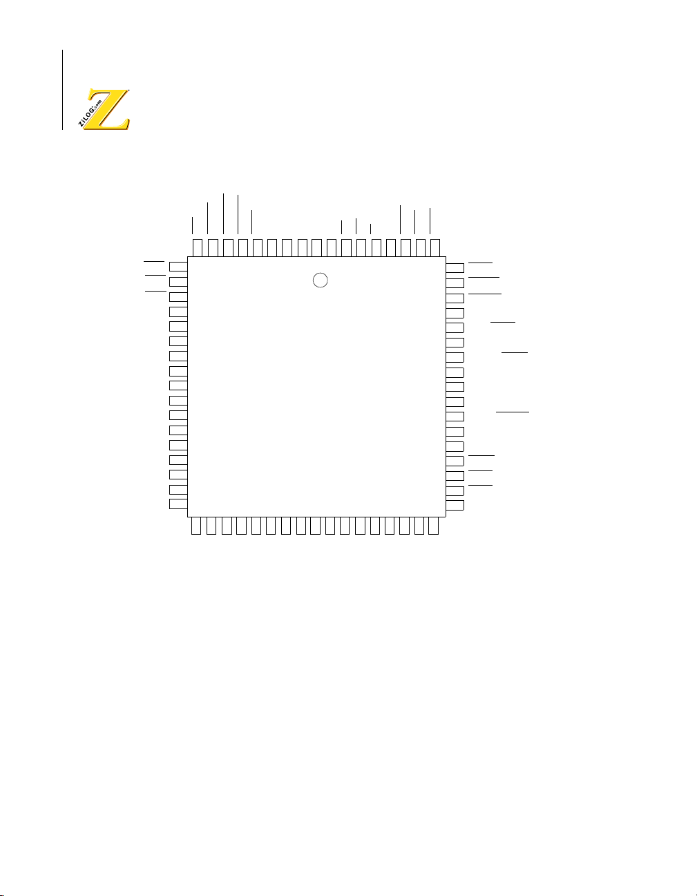
Figure 1. 64-Pin DIP . . . . . . . . . . . . . . . . . . . . . . . . . . . . . . . . . . . . . . .3
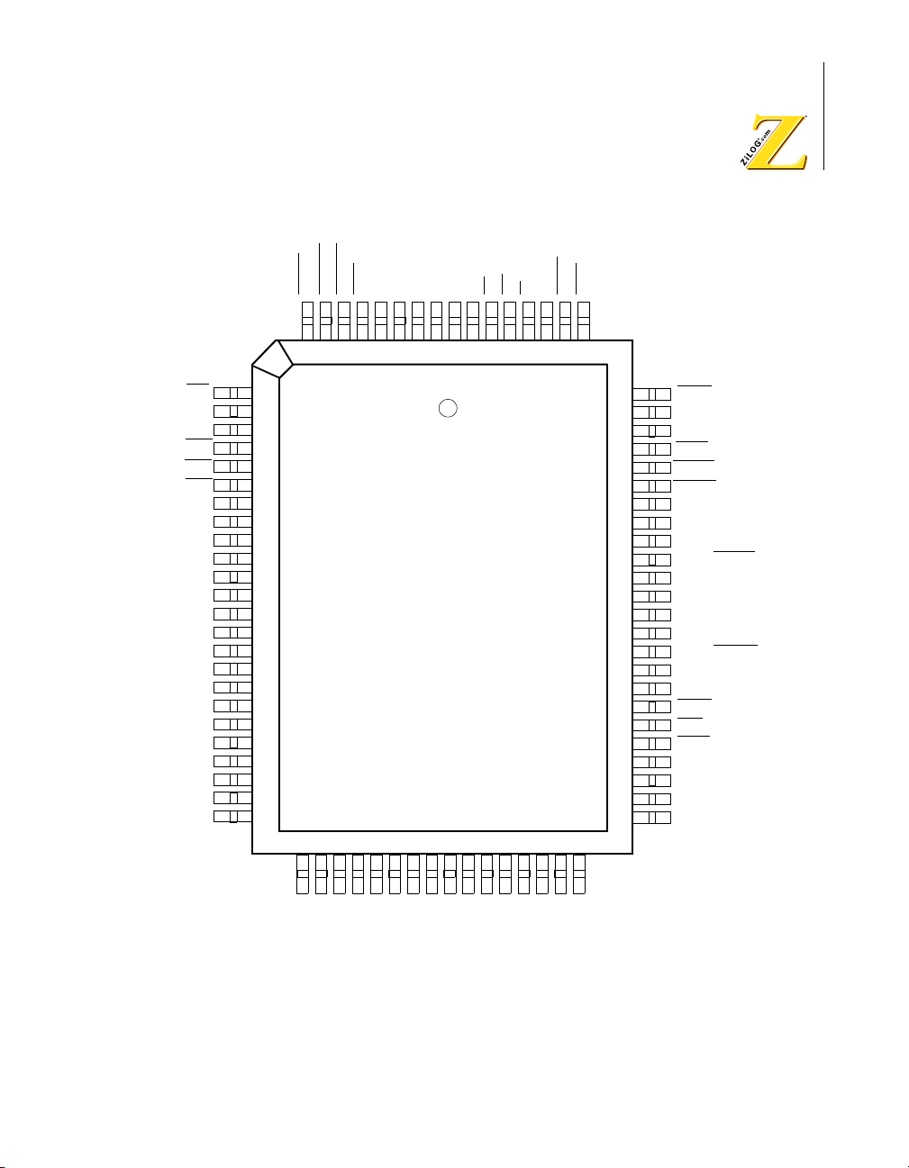
Figure 2. 68-Pin PLCC . . . . . . . . . . . . . . . . . . . . . . . . . . . . . . . . . . . . .4
Figure 3. 80-Pin QFP . . . . . . . . . . . . . . . . . . . . . . . . . . . . . . . . . . . . . .5
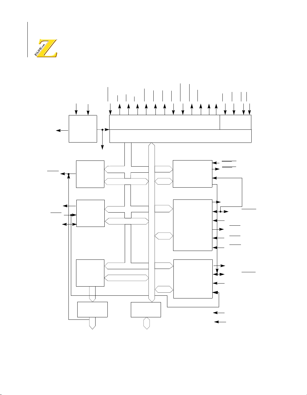
Figure 4. Z80180/Z8S180/Z8L180 Block Diagram . . . . . . . . . . . . . . .6
Figure 5. Operation Mode Control Register . . . . . . . . . . . . . . . . . . . .15
Figure 6. M1 Temporary Enable Timing . . . . . . . . . . . . . . . . . . . . . .16
Figure 7. I/O Read and Write Cycles with IOC = 1
Timing Diagram . . . . . . . . . . . . . . . . . . . . . . . . . . . . . . . . .17
Figure 8. I/O Read and Write cycles with IOC = 0
Timing Diagram . . . . . . . . . . . . . . . . . . . . . . . . . . . . . . . . .17
Figure 9. Op Code Fetch (without Wait State) Timing Diagram . . . .19
Figure 10. Op Code Fetch (with Wait State) Timing Diagram . . . . . .20
Figure 11. Memory Read/Write (without Wait State)
Timing Diagram . . . . . . . . . . . . . . . . . . . . . . . . . . . . . . . . .21
Figure 12. Memory Read/Write (with Wait State)
Timing Diagram . . . . . . . . . . . . . . . . . . . . . . . . . . . . . . . . .22
Figure 13. I/O Read/Write Timing Diagram . . . . . . . . . . . . . . . . . . . .23
Figure 14. Instruction Timing Diagram . . . . . . . . . . . . . . . . . . . . . . . .24
Figure 15. RESET Timing Diagram . . . . . . . . . . . . . . . . . . . . . . . . . . .25
Figure 16. Bus Exchange Timing During Memory Read . . . . . . . . . . .26
Figure 17. Bus Exchange Timing During CPU Internal Operation . . .27
Figure 18. WAIT Timing Diagram . . . . . . . . . . . . . . . . . . . . . . . . . . .28
Figure 19. Memory and I/O Wait State Insertion
(DCNTL – DMA/Wait Control Register) . . . . . . . . . . . . . .29
Figure 20. HALT Timing Diagram . . . . . . . . . . . . . . . . . . . . . . . . . . .33
ix
UM005003-0703
Page 9

Z8018x
Family MPU User Manual
x
Figure 21. SLEEP Timing Diagram . . . . . . . . . . . . . . . . . . . . . . . . . . 35
Figure 22. I/O Address Relocation . . . . . . . . . . . . . . . . . . . . . . . . . . . 43
Figure 23. Logical Address Mapping Examples . . . . . . . . . . . . . . . . . 55
Figure 24. Physical Address Transition . . . . . . . . . . . . . . . . . . . . . . . 56
Figure 25. MMU Block Diagram . . . . . . . . . . . . . . . . . . . . . . . . . . . . 56
Figure 26. I/O Address Translation . . . . . . . . . . . . . . . . . . . . . . . . . . . 57
Figure 27. Logical Memory Organization . . . . . . . . . . . . . . . . . . . . . 58
Figure 28. Logical Space Configuration . . . . . . . . . . . . . . . . . . . . . . . 59
Figure 29. Physical Address Generation . . . . . . . . . . . . . . . . . . . . . . . 64
Figure 30. Physical Address Generation 2 . . . . . . . . . . . . . . . . . . . . . 64
Figure 31. Interrupt Sources . . . . . . . . . . . . . . . . . . . . . . . . . . . . . . . . 65
Figure 32. TRAP Timing Diagram -2nd Op Code Undefined . . . . . . 71
Figure 33. TRAP Timing - 3rd Op Code Undefined . . . . . . . . . . . . . 72
Figure 34. NMI Use . . . . . . . . . . . . . . . . . . . . . . . . . . . . . . . . . . . . . . 74
Figure 35. NMI Timing . . . . . . . . . . . . . . . . . . . . . . . . . . . . . . . . . . . . 75
Figure 36. INT0 Mode 0 Timing Diagram . . . . . . . . . . . . . . . . . . . . . 76
Figure 37. INT0 Mode 1 Interrupt Sequence . . . . . . . . . . . . . . . . . . . 77
Figure 38. INT0 Mode 1 Timing . . . . . . . . . . . . . . . . . . . . . . . . . . . . 78
Figure 39. INT0 Mode 2 Vector Acquisition . . . . . . . . . . . . . . . . . . . 79
Figure 40. INT0 Interrupt Mode 2 Timing Diagram . . . . . . . . . . . . . 80
Figure 41. INT1, INT2 Vector Acquisition . . . . . . . . . . . . . . . . . . . . 81
Figure 42. RETI Instruction Sequence . . . . . . . . . . . . . . . . . . . . . . . . 84
Figure 43. INT1, INT2 and Internal Interrupts Timing Diagram . . . . 86
Figure 44. Refresh Cycle Timing Diagram . . . . . . . . . . . . . . . . . . . . . 87
Figure 45. DMAC Block Diagram . . . . . . . . . . . . . . . . . . . . . . . . . . . 93
Figure 46. DMA Timing Diagram-CYCLE STEAL Mode . . . . . . . 106
Figure 47. CPU Operation and DMA Operation DREQ0
Figure 48. CPU Operation and DMA Operation DREQ0
is Programmed for Level-Sense . . . . . . . . . . . . . . . . . . . 107
is Programmed for Edge-Sense . . . . . . . . . . . . . . . . . . . . 108
UM005003-0703
Page 10

Z8018x
Family MPU User Manual
Figure 49. TEND0 Output Timing Diagram . . . . . . . . . . . . . . . . . . .108
Figure 50. DMA Interrupt Request Generation . . . . . . . . . . . . . . . . .114
Figure 51. NMI and DMA Operation Timing Diagram . . . . . . . . . . .115
Figure 52. ASCI Block Diagram . . . . . . . . . . . . . . . . . . . . . . . . . . . .117
Figure 53. DCD0 Timing Diagram . . . . . . . . . . . . . . . . . . . . . . . . . .139
Figure 54. RTS0 Timing Diagram . . . . . . . . . . . . . . . . . . . . . . . . . . .140
Figure 55. ASCI Interrupt Request Circuit Diagram . . . . . . . . . . . . .140
Figure 56. ASCI Clock . . . . . . . . . . . . . . . . . . . . . . . . . . . . . . . . . . . .141
Figure 57. CSI/O Block Diagram . . . . . . . . . . . . . . . . . . . . . . . . . . . .147
Figure 58. CSI/O Interrupt Request Generation . . . . . . . . . . . . . . . . .151
Figure 59. Transmit Timing Diagram–Internal Clock . . . . . . . . . . . .153
Figure 60. Transmit Timing–External Clock . . . . . . . . . . . . . . . . . . .154
Figure 61. CSI/O Receive Timing–Internal Clock . . . . . . . . . . . . . . .155
Figure 62. CSI/O Receive Timing–External Clock . . . . . . . . . . . . . .156
Figure 63. PRT Block Diagram . . . . . . . . . . . . . . . . . . . . . . . . . . . . .157
Figure 64. Timer Initialization, Count Down, and Reload
Timing Diagram . . . . . . . . . . . . . . . . . . . . . . . . . . . . . . . .163
Figure 65. Timer Output Timing Diagram . . . . . . . . . . . . . . . . . . . . .164
Figure 66. PRT Interrupt Request Generation . . . . . . . . . . . . . . . . . .164
Figure 67. E Clock Timing Diagram (During Read/Write Cycle
and Interrupt Acknowledge Cycle . . . . . . . . . . . . . . . . . .167
Figure 68. E Clock Timing in BUS RELEASE Mode . . . . . . . . . . . .167
Figure 69. E Clock Timing in SLEEP Mode and
SYSTEM STOP Mode . . . . . . . . . . . . . . . . . . . . . . . . . . .168
Figure 70. External Clock Interface . . . . . . . . . . . . . . . . . . . . . . . . . .169
Figure 71. Clock Generator Circuit . . . . . . . . . . . . . . . . . . . . . . . . . .170
Figure 72. Circuit Board Design Rules . . . . . . . . . . . . . . . . . . . . . . .170
Figure 73. Example of Board Design . . . . . . . . . . . . . . . . . . . . . . . . .171
xi
UM005003-0703
Page 11

Z8018x
Family MPU User Manual
xii
Software Architecture . . . . . . . . . . . . . . . . . . . . . . . . . . . . . . . . . . 173
Figure 74. CPU Register Configurations . . . . . . . . . . . . . . . . . . . . . 176
Figure 75. Register Direct — Bit Field Definitions . . . . . . . . . . . . . 181
Figure 76. Register Indirect Addressing . . . . . . . . . . . . . . . . . . . . . . 181
Figure 77. Indexed Addressing . . . . . . . . . . . . . . . . . . . . . . . . . . . . . 182
Figure 78. Extended Addressing . . . . . . . . . . . . . . . . . . . . . . . . . . . . 182
Figure 79. Immediate Addressing . . . . . . . . . . . . . . . . . . . . . . . . . . . 183
Figure 80. Relative Addressing . . . . . . . . . . . . . . . . . . . . . . . . . . . . . 183
Timing Diagrams . . . . . . . . . . . . . . . . . . . . . . . . . . . . . . . . . . . . . . 197
Figure 81. AC Timing Diagram 1 . . . . . . . . . . . . . . . . . . . . . . . . . . . 197
Figure 82. AC Timing Diagram 2 . . . . . . . . . . . . . . . . . . . . . . . . . . . 198
Figure 83. CPU Timing (IOC = 0) (I/O Read Cycle,
I/O Write Cycle) . . . . . . . . . . . . . . . . . . . . . . . . . . . . . . . 199
Figure 84. DMA Control Signals . . . . . . . . . . . . . . . . . . . . . . . . . . . 200
Figure 85. E Clock Timing (Memory R/W Cycle) (I/O R/W Cycle) 201
Figure 86. E Clock Timing (BUS RELEASE Mode, SLEEP Mode, and
SYSTEM STOP Mode . . . . . . . . . . . . . . . . . . . . . . . . . . 201
Figure 87. E Clock Timing (Minimum Timing Example of PWEL and
PWEH) . . . . . . . . . . . . . . . . . . . . . . . . . . . . . . . . . . . . . . . 202
Figure 88. Timer Output Timing . . . . . . . . . . . . . . . . . . . . . . . . . . . . 202
Figure 89. SLP Execution Cycle Timing Diagram . . . . . . . . . . . . . . 203
Figure 90. CSI/O Receive/Transmit Timing Diagram . . . . . . . . . . . 204
Figure 91. External Clock Rise Time and Fall Time . . . . . . . . . . . . 204
Figure 92. Input Rise Time and Fall Time
(Except EXTAL, RESET) . . . . . . . . . . . . . . . . . . . . . . . . 204
Figure 93. Test Setup . . . . . . . . . . . . . . . . . . . . . . . . . . . . . . . . . . . . 205
UM005003-0703
Page 12

Z8018x
Family MPU User Manual
List of Tables
Z80180, Z8S180, Z8L180 MPU Operation . . . . . . . . . . . . . . . . . . . .1
Table 1. Status Summary . . . . . . . . . . . . . . . . . . . . . . . . . . . . . . . . .10
Table 2. Multiplexed Pin Descriptions . . . . . . . . . . . . . . . . . . . . . . .12
Table 3. Memory Wait States . . . . . . . . . . . . . . . . . . . . . . . . . . . . . .29
Table 4. Wait State Insertion . . . . . . . . . . . . . . . . . . . . . . . . . . . . . . .30
Table 5. Power-Down Modes
(Z8S180/Z8L180-Class Processor Only) . . . . . . . . . . . . . .37
Table 6. I/O Address Map for Z80180-Class Processors Only . . . . .44
Table 7. I/O Address Map
(Z8S180/Z8L180-Class Processors Only) . . . . . . . . . . . . .48
Table 8. State of IEF1 and IEF2. . . . . . . . . . . . . . . . . . . . . . . . . . . . .69
Table 9. Vector Table . . . . . . . . . . . . . . . . . . . . . . . . . . . . . . . . . . . .82
Table 10. RETI Control Signal States . . . . . . . . . . . . . . . . . . . . . . . . .85
Table 11. DRAM Refresh Intervals . . . . . . . . . . . . . . . . . . . . . . . . . .89
Table 12. Channel 0 Destination . . . . . . . . . . . . . . . . . . . . . . . . . . . . .98
Table 13. Channel 0 Source . . . . . . . . . . . . . . . . . . . . . . . . . . . . . . . .99
Table 14. Transfer Mode Combinations . . . . . . . . . . . . . . . . . . . . . . .99
Table 15. Channel 1 Transfer Mode . . . . . . . . . . . . . . . . . . . . . . . . .102
Table 16. DMA Transfer Request . . . . . . . . . . . . . . . . . . . . . . . . . . .110
Table 17. Data Formats . . . . . . . . . . . . . . . . . . . . . . . . . . . . . . . . . . .131
Table 18. Divide Ratio . . . . . . . . . . . . . . . . . . . . . . . . . . . . . . . . . . .134
Table 19. ASCI Baud Rate Selection. . . . . . . . . . . . . . . . . . . . . . . . .142
Table 20. Clock Mode Bit Values . . . . . . . . . . . . . . . . . . . . . . . . . . .144
Table 21. 2^ss Values . . . . . . . . . . . . . . . . . . . . . . . . . . . . . . . . . . . .145
Table 22. CSI/O Baud Rate Selection . . . . . . . . . . . . . . . . . . . . . . . .150
xiv
UM005003-0703
Page 13

Z8018x
Family MPU User Manual
Table 23. Timer Output Control . . . . . . . . . . . . . . . . . . . . . . . . . . . .163
Table 24. E Clock Timing in Each Condition . . . . . . . . . . . . . . . . . .166
Table 25. Z8X180 Operating Frequencies . . . . . . . . . . . . . . . . . . . .169
Software Architecture . . . . . . . . . . . . . . . . . . . . . . . . . . . . . . . . . . .173
Table 26. Instruction Set Summary . . . . . . . . . . . . . . . . . . . . . . . . . .173
DC Characteristics . . . . . . . . . . . . . . . . . . . . . . . . . . . . . . . . . . . . .185
Table 27. Absolute Maximum Rating . . . . . . . . . . . . . . . . . . . . . . . .185
Table 28. Z80180 DC Characteristics . . . . . . . . . . . . . . . . . . . . . . . .186
Table 29. Z8S180 DC Characteristics . . . . . . . . . . . . . . . . . . . . . . . .187
Table 30. Z8L180 DC Characteristics . . . . . . . . . . . . . . . . . . . . . . . .189
xv
AC Characteristics . . . . . . . . . . . . . . . . . . . . . . . . . . . . . . . . . . . . .193
Table 31. Z8S180 AC Characteristics . . . . . . . . . . . . . . . . . . . . . . . 193
Instruction Set . . . . . . . . . . . . . . . . . . . . . . . . . . . . . . . . . . . . . . . . .207
Table 32. Register Values . . . . . . . . . . . . . . . . . . . . . . . . . . . . . . . . .207
Table 33. Bit Values . . . . . . . . . . . . . . . . . . . . . . . . . . . . . . . . . . . . .208
Table 34. Instruction Values . . . . . . . . . . . . . . . . . . . . . . . . . . . . . . .208
Table 35. Address Values . . . . . . . . . . . . . . . . . . . . . . . . . . . . . . . . .209
Table 36. Flag Conditions . . . . . . . . . . . . . . . . . . . . . . . . . . . . . . . . .209
Table 37. Operations Mnemonics . . . . . . . . . . . . . . . . . . . . . . . . . . .210
Table 38. Arithmetic and Logical Instructions (8-bit) . . . . . . . . . . . .211
Table 39. Rotate and Shift Instructions . . . . . . . . . . . . . . . . . . . . . . .216
Table 40. Arithmetic Instructions (16-bit) . . . . . . . . . . . . . . . . . . . . .221
Table 41. 8-Bit Load . . . . . . . . . . . . . . . . . . . . . . . . . . . . . . . . . . . . .222
Table 42. 16-Bit Load . . . . . . . . . . . . . . . . . . . . . . . . . . . . . . . . . . . .223
UM005003-0703
Page 14

Z8018x
Family MPU User Manual
xvi
Table 43. Block Transfer . . . . . . . . . . . . . . . . . . . . . . . . . . . . . . . . . 225
Table 44. Stock and Exchange . . . . . . . . . . . . . . . . . . . . . . . . . . . . . 227
Table 45. Program Control Instructions . . . . . . . . . . . . . . . . . . . . . . 229
Table 46. I/O Instructions. . . . . . . . . . . . . . . . . . . . . . . . . . . . . . . . . 231
Table 47. Special Control Instructions . . . . . . . . . . . . . . . . . . . . . . . 235
Op Code Map . . . . . . . . . . . . . . . . . . . . . . . . . . . . . . . . . . . . . . . . . 247
Table 48. 1st Op Code Map Instruction Format: XX . . . . . . . . . . . 247
Table 49. 2nd Op Code Map Instruction Format: CB XX . . . . . . . 249
Table 50. 2nd Op Code Map Instruction Format: ED XX . . . . . . . 250
Bus Control Signal Conditions . . . . . . . . . . . . . . . . . . . . . . . . . . . 251
Table 51. Bus and Control Signal Condition in Each
Machine Cycle . . . . . . . . . . . . . . . . . . . . . . . . . . . . . . . . . 251
Table 52. Interrupts. . . . . . . . . . . . . . . . . . . . . . . . . . . . . . . . . . . . . . 279
Operating Modes Summary . . . . . . . . . . . . . . . . . . . . . . . . . . . . . . 281
Table 53. Request Acceptances in Each Operating Mode . . . . . . . . 281
Table 54. The Z80180 Types of Requests . . . . . . . . . . . . . . . . . . . . 282
Status Signals 287
Table 55. Pin Outputs in Each Operating Mode. . . . . . . . . . . . . . . . 287
Table 56. Pin Status During RESET and
LOW POWER OPERATION Modes. . . . . . . . . . . . . . . . 289
I/O Registers . . . . . . . . . . . . . . . . . . . . . . . . . . . . . . . . . . . . . . . . . . 293
Table 57. Internal I/O Registers . . . . . . . . . . . . . . . . . . . . . . . . . . . . 293
UM005003-0703
Page 15

Z8018x
Family MPU User Manual
xv
UM005003-0703
Page 16

Family MPU User Manual
Z80180, Z8S180, Z8L180 MPU Operation
FEATURES
•
Operating Frequency to 33 MHz
•
On-Chip MMU Supports Extended Address Space
•
Two DMA Channels
•
On-Chip Wait State Generators
•
Two Universal Asynchronous Receiver/Transmitter (UART) Channels
•
Two 16-Bit Timer Channels
Z8018x
1
•
On-Chip Interrupt Controller
•
On-Chip Clock Oscillator/Generator
•
Clocked Serial I/O Port
•
Code Compatible with ZiLOG Z80 CPU
•
Extended Instructions
GENERAL DESCRIPTION
Based on a microcoded execution unit and an advanced CMOS
manufacturing technology, the Z80180, Z8S180, Z8L180 (Z8X180) is an
8-bit MPU which provides the benefits of reduced system costs and low
power operation while offering higher performance and maintaining
compatibility with a large base of industry standard software written
around the ZiLOG Z8X CPU.
Higher performance is obtained by virtue of higher operating frequencies,
reduced instruction execution times, an enhanced instruction set, and an
UM005003-0703
Page 17

Z8018x
Family MPU User Manual
2
on-chip memory management unit (MMU) with the capability of
addressing up to 1 MB of memory.
Reduced system costs are obtained by incorporating several key system
functions on-chip with the CPU. These key functions include I/O devices
such as DMA, UART, and timer channels. Also included on-chip are
several glue functions such as dynamic RAM refresh control, wait state
generators, clock oscillator, and interrupt controller.
Not only does the Z8X180 consume a low amount of power during
normal operation, but processors with Z8S180 and Z8L180 class
processors also provides two operating modes that are designed to
drastically reduce the power consumption even further. The SLEEP mode
reduces power by placing the CPU into a stopped state, thereby
consuming less current, while the on-chip I/O device is still operating.
The SYSTEM STOP mode places both the CPU and the on-chip
peripherals into a stopped state, thereby reducing power consumption
even further.
When combined with other CMOS VLSI devices and memories, the
Z8X180 provides an excellent solution to system applications requiring
high performance, and low power operation.
Figures 1 through 3 illustrate the three pin packages in the Z8X180 MPU
family:
•
64-Pin Dual In-line Package (DIP), Figure 1
•
68-Pin Plastic Leaded Chip Carrier (PLCC), Figure 2
•
80-Pin Quad Flat Pack (QFP), Figure 3
Pin out package descriptions for other Z8X180-based products are
covered in their respective product specifications.
Figure 4 depicts the block diagram that is shared throughout all
configurations of the Z8X180.
UM005003-0703
Page 18

V
XTAL
EXTAL
WAIT
BUSACK
BUSREQ
RESET
NMI
INT0
INT1
INT2
ST
A0
A1
A2
A3
A4
A5
A6
A7
A8
A9
A10
A11
A12
A13
A14
A15
A16
A17
A18/TOUT
V
CC
Z8018x
Family MPU User Manual
3
1
SS
2
3
4
5
6
7
8
9
10
11
12
13
14
15
16
17
18
19
20
21
22
23
24
25
26
27
28
29
30
31
32
Z8X180
64
Phi
RD
63
62
WR
61
MI
E
60
59
MREQ
58
IORQ
57
RFSH
56
HALT
55
TEND1
54
DREQ1
53
CKS
52
RXS/CTS1
51
TXS
50
CKA1/TEND0
RXA1
49
48
TXA1
CKA0/DREQ0
47
46
RXA0
45
TXA0
44
DCO0
CTS0
43
RTS0
42
D7
41
40
D6
D5
39
38
D4
37
D3
36
D2
D1
35
34
D0
33
V
SS
Figure 1. 64-Pin DIP
UM005003-0703
Page 19
Z8018x
Family MPU User Manual
4
10
INT0
INT1
11
INT2
12
ST
13
A0
14
A1
15
A2
16
17
A3
18
V
SS
A4
19
20
A5
A6
21
A7
22
A8
23
A9
24
A10
25
26
A11
NMI
9
27
A12
RESET
8
28
A13
BUSREQ
7
29
A14
BUSACK
6
30
A15
WAIT
5
A16
EXTAL
XTAL
432
Z8X180
33
32
A17
VSS
VLS
PhiRDWRMIE
1
68676665646362
35
34
363137383940414243
SS
CC
D0
D2
D1
V
A19
V
D3
D4
MREQ
IORQ
RFSH
61
60
HALT
TEND1
59
58
DREQ1
57
CKS
RXS/CTS1
56
55
TXS
54
CKA1/TEND0
53
RXA1
52
TEST
51
TXA1
50
CKA0/DREQ0
49
RXA0
48
TXA0
47
DCD0
46
CTS0
RTS0
45
44
D7
D6
D5
A18/TOUT
Figure 2. 68-Pin PLCC
UM005003-0703
Page 20
SSVSS
K
RESET
BUSREQBUSAC
8079787776757473727170
EXTALNCWAIT
XTAL
V
Phi
RD
WR
69
Family MPU User Manual
MREQ
MI
686766
IORQ
E
65
Z8018x
5
NMI
NC
NC
INT0
INT1
INT2
ST
A0
A1
A2
A3
V
SS
A4
NC
A5
A6
A7
A8
A9
A10
A11
NC
NC
A12
1
2
3
4
5
6
7
8
9
10
11
12
13
14
15
16
17
18
19
20
21
22
23
24
10111213141516
A13
A14
A15
A16
Z8X180
NC
A17
17
CC
V
181920
SS
A19
V
D0
21
D1
222324
D2D3D4
64
63
62
61
60
59
58
57
56
55
54
53
52
51
50
49
48
47
46
45
44
43
42
41
25
D5
RFSH
NC
NC
HALT
TEND1
DREQ1
CKS
RXS/CTS1
TXS
CKA1/TEND0
RXA1
TEST
TXA1
NC
CKA0/DREQ0
RXA0
TXA0
DCD0
CTS
RTS0
D7
NC
NC
D6
Figure 3. 80-Pin QFP
A18/TOUT
UM005003-0703
Page 21
Z8018x
Family MPU User Manual
6
XTAL
EXTAL
RESETRDWRMIMREQ
IORQ
HALT
WAIT
BUSREQ
BUSACK
RFSH
STENMI
INT0
INT1
INT2
Phi
A18/TOUT
TXS
RXS/CTS1
CKS
Timing
Generator
16-bit
Programmable
Reload
Timers
Clocked
Serial I/O
Port
MMU
(16-bit)
Address Bus
Bus State Control
CPU
Data Bus (8-bit)
DMACs
(2)
Asynchronous
SCI
(Channel 0)
Asynchronous
SCI
(channel 1)
Interrupt
DREQ1
TEND1
TXA0
CKA0/DREQ0
RXA0
RTS0
CTS0
DCD0
TXA1
CKA1/TEND0
RXA1
Address
Buffer
–
A0
A19
Data
Buffer
D0
–
DF
Figure 4. Z80180/Z8S180/Z8L180 Block Diagram
UM005003-0703
V
CC
V
SS
Page 22

PIN DESCRIPTION
A0–A19. Address Bus (Output, Active High, 3-state). A0–A19 form a 20-
bit address bus. The Address Bus provides the address for memory data
bus exchanges, up to 1 MB, and I/O data bus exchanges, up to 64K. The
address bus enters a high impedance state during RESET and external bus
acknowledge cycles. Address line A18 is multiplexed with the output of
PRT channel 1 (TOUT, selected as address output on RESET) and address
line A19 is not available in DIP versions of the Z8X180.
Z8018x
Family MPU User Manual
7
BUSACK
that the requesting device, the MPU address and data bus, and some
control signals, have entered their high impedance state.
BUSREQ
external devices (such as DMA controllers) to request access to the
system bus. This request has a higher priority than NMI
recognized at the end of the current machine cycle. This signal stops the
CPU from executing further instructions and places the address and data
buses, and other control signals, into the high impedance state.
CKA0, CKA1. Asynchronous Clock 0 and 1 (Bidirectional, Active High).
These pins are the transmit and receive clocks for the ASCI channels.
CKA0, is multiplexed with DRE
TEND
CKS. Serial Clock (Bidirectional, Active High). This line is the clock for
the CSIO channel.
CLOCK (PHI). System Clock (Output, Active High). The output is used
as a reference clock for the MPU and the external system. The frequency
of this output is equal to one-half that of the crystal or input clock
frequency.
CTS
modem control signals for the ASCI channels. CTS
. Bus Acknowledge (Output, Active Low). BUSACK indicates
. Bus Request (Input, Active Low). This input is used by
and is always
Q0 and CKA1 is multiplexed with
0.
0, CTS1. Clear to Send 0 and 1 (Inputs, Active Low). These lines are
1 is multiplexed with RXS.
UM005003-0703
Page 23

Z8018x
Family MPU User Manual
8
D0–D7. Data Bus (Bidirectional, Active High, 3-state). D0-D7 constitute
an 8-bit bidirectional data bus, used for the transfer of information to and
from I/O and memory devices. The data bus enters the high impedance
state during RESET and external bus acknowledge cycles.
DCD
programmable modem control signal for ASCI channel 0.
0. Data Carrier Detect 0 (Input, Active Low). This input is a
DREQ
0, DREQ1. DMA Request 0 and 1 (Input, Active Low). DREQ is
used to request a DMA transfer from one of the on-chip DMA channels.
The DMA channels monitor these inputs to determine when an external
device is ready for a read or write operation. These inputs can be
programmed to be either level- or edge-sensed. DREQ
0 is multiplexed
with CKA0.
E. Enable Clock (Output, Active High). Synchronous machine cycle clock
output during bus transactions.
EXTAL. External Clock/Crystal (Input, Active High). Crystal oscillator
connection. An external clock can be input to the Z8X180 on this pin
when a crystal is not used. This input is Schmitt-triggered.
HALT
after the CPU has executed either the HALT
. Halt/Sleep Status (Output, Active Low). This output is asserted
or SLP instruction, and is
waiting for either non-maskable or maskable interrupt before operation
can resume. HALT
is also used with the M1 and ST signals to decode
status of the CPU machine cycle.
0. Maskable Interrupt Request 0 (Input, Active Low). This signal is
INT
generated by external I/O devices. The CPU honors this request at the end
of the current instruction cycle as long as the NMI
and BUSREQ signals
are inactive. The CPU acknowledges this interrupt request with an
interrupt acknowledge cycle. During this cycle, both the M
1 and IORQ
signals become Active.
1, INT2. Maskable Interrupt Requests 1 and 2 (Inputs, Active Low).
INT
This signal is generated by external I/O devices. The CPU honors these
requests at the end of the current instruction cycle as long as the NMI
UM005003-0703
,
Page 24

Z8018x
Family MPU User Manual
BUSREQ, and INT0 signals are inactive. The CPU acknowledges these
interrupt requests with an interrupt acknowledge cycle. Unlike the
acknowledgment for INT
0, during this cycle neither the M1 or IORQ
signals become Active.
. I/O Request (Output, Active Low, 3-state). IORQ indicates that the
IORQ
address bus contains a valid I/O address for an I/O read or I/O write
operation. IORQ
acknowledgment of the INT
is also generated, along with M1, during the
0 input signal to indicate that an interrupt
response vector can be placed onto the data bus. This signal is analogous
to the IOE
1. Machine Cycle 1 (Output, Active Low). Together with MR EQ , M1
M
signal of the Z64180.
indicates that the current cycle is the Op Code fetch cycle of an
instruction execution. Together with IORQ
cycle is for an interrupt acknowledge. It is also used with the HALT
, M1 indicates that the current
and
ST signal to decode status of the CPU machine cycle. This signal is
analogous to the LIR
signal of the Z64180.
9
MREQ
. Memory Request (Output, Active Low, 3-state). MREQ indicates
that the address bus holds a valid address for a memory read or memory
write operation. This signal is analogous to the ME
. Non-maskable Interrupt (Input, negative edge triggered). NMI has
NMI
a higher priority than INT
and is always recognized at the end of an
signal of the Z64180.
instruction, regardless of the state of the interrupt enable flip-flops. This
signal forces CPU execution to continue at location
. Read (Output active Low, 3-state). RD indicates that the CPU wants
RD
0066H.
to read data from memory or an I/O device. The addressed I/O or memory
device must use this signal to gate data onto the CPU data bus.
. Refresh (Output, Active Low). Together with MREQ, RFSH
RFSH
indicates that the current CPU machine cycle and the contents of the
address bus must be used for refresh of dynamic memories. The low order
8 bits of the address bus (A7–A0) contain the refresh address.
This signal is analogous to the REF
signal of the Z64180.
UM005003-0703
Page 25

10
Z8018x
Family MPU User Manual
RTS0. Request to Send 0 (Output, Active Low). This output is a
programmable modem control signal for ASCI channel 0.
RXA0, RXA1. Receive Data 0 and 1 (Inputs, Active High). These signals
are the receive data to the ASCI channels.
RXS. Clocked Serial Receive Data (Input, Active High). This line is the
receiver data for the CSIO channel. RXS is multiplexed with the CTS
signal for ASCI channel 1.
1
ST. Status (Output, Active High). This signal is used with the M1
HALT
output to decode the status of the CPU machine cycle. Table 1
and
provides status summary.
Table 1. Status Summary
ST HALT
0 1 0 CPU operation (1st Op Code fetch)
1 1 0 CPU operation (2nd Op Code and 3rd Op Code fetch)
1 1 1 CPU operation (MC
0X
0 0 0 HALT mode
1 0 1 SLEEP mode (including SYSTEM STOP mode)
1
M1 Operation
1 DMA operation
2
except for Op Code fetch)
1. X = Don't care
2. MC = Machine cycle
TEND
0, TEND1. Transfer End 0 and 1 (Outputs, Active Low). This
output is asserted active during the last write cycle of a DMA operation. It
is used to indicate the end of the block transfer. TEND
0 in multiplexed
with CKA1.
TEST. Test (Output, not on DIP version). This pin is for test and must be
left open.
UM005003-0703
Page 26

Z8018x
Family MPU User Manual
TOUT. Timer Out (Output, Active High). TOUT is the pulse output from
PRT channel 1. This line is multiplexed with A18 of the address bus.
TXA0, TXA1. Transmit Data 0 and 1 (Outputs, Active High). These
signals are the transmitted data from the ASCI channels. Transmitted data
changes are with respect to the falling edge of the transmit clock.
TXS. Clocked Serial Transmit Data (Output, Active High). This line is
the transmitted data from the CSIO channel.
. Wait (Input; Active Low). WAIT indicates to the CPU that the
WAIT
addressed memory or I/O devices are not ready for a data transfer. This
input is used to induce additional clock cycles into the current machine
cycle. The WAIT
input is sampled on the falling edge of T2 (and
subsequent Wait States). If the input is sampled Low, then additional Wait
States are inserted until the WAIT
input is sampled High, at which time
execution continues.
11
. Write (Output, Active Low, 3-state). WR indicates that the CPU data
WR
bus holds valid data to be stored at the addressed I/O or memory location.
XTAL. Crystal (Input, Active High). Crystal oscillator connection. This
pin must be left open if an external clock is used instead of a crystal. The
oscillator input is not a TTL level (reference DC characteristics).
Multiplexed pins are described in Table 2.
UM005003-0703
Page 27

12
Z8018x
Family MPU User Manual
Table 2. Multiplexed Pin Descriptions
Multiplexed
Pins Descriptions
A18/TOUT
CKA0/
DREQ0
TEND0
CKA1/
During RESET, this pin is initialized as A18 pin. If either
TOC1 or TOC0 bit of the Timer Control Register (TCR) is set
to 1, TOUT function is selected. If TOC1 and TOC0 bits are
cleared to 0, A18 function is selected.
During RESET, this pin is initialized as CKA0 pin.
If either DM1 or SM1 in DMA Mode Register (DMODE) is
set to 1,
During RESET, this pin is initialized as CKA1 pin. If
CKA1D bit in ASCI control register ch 1 (CNTLA1) is set to
1,
CKA1 function is selected.
DREQ0 function is always selected.
TEND0 function is selected. If CKA1D bit is set to 0,
During RESET, this pin is initialized as RXS pin. If CTS1E bit
RXS/
CTS1
in ASCI status register ch 1 (STAT1) is set to 1,
is selected. If CTS1E bit is 0, RXS function is selected.
ARCHITECTURE
The Z8X180 combines a high performance CPU core with a variety of
system and I/O resources useful in a broad range of applications. The CPU
core consists of five functional blocks: clock generator, bus state controller
(including dynamic memory refresh), interrupt controller, memory
management unit (MMU), and the central processing unit (CPU). The
integrated I/O resources make up the remaining four functional blocks:
•
Direct Memory Access (DMA) Control (2 channels)
•
Asynchronous Serial Communications Interface (ASCI, 2 channels),
UM005003-0703
CTS1 function
Page 28

Z8018x
Family MPU User Manual
•
Programmable Reload Timers (PRT, 2 channels)
•
Clock Serial I/O (CSIO) channel.
Other Z8X180 family members (such as Z80183, Z80S183, Z80185/195)
feature, in addition to these blocks, additional peripherals and are covered
in their associated Product Specification
Clock Generator
This logic generates the system clock from either an external crystal or
clock input. The external clock is divided by two and provided to both
internal and external devices.
Bus State Controller
13
This logic performs all of the status and bus control activity associated
with both the CPU and some on-chip peripherals. This includes Wait State
timing, RESET cycles, DRAM refresh, and DMA bus exchanges.
Interrupt Controller
This block monitors and prioritizes the variety of internal and external
interrupts and traps to provide the correct responses from the CPU. To
remain compatible with the Z80 CPU, three different interrupt modes are
supported.
Memory Management Unit
The MMU allows the user to map the memory used by the CPU (logically
only 64K) into the 1MB addressing range supported by the Z8X180. The
organization of the MMU object code features compatibility with the Z80
CPU while offering access to an extended memory space. This capability
is accomplished by using an effective common area - banked area
scheme.
UM005003-0703
Page 29

14
Z8018x
Family MPU User Manual
Central Processing Unit
The CPU is microcoded to provide a core that is object code compatible
with the Z80 CPU. It also provides a superset of the Z80 instruction set,
including 8-bit multiply and divide. This core has been enhanced to allow
many of the instructions to execute in fewer clock cycles.
DMA Controller
The DMA controller provides high speed transfers between memory and
I/O devices. Transfer operations supported are memory-to-memory,
memory to/from I/O and I/O to I/O. Transfer modes supported are
REQUEST, BURST, and CYCLE STEAL. DMA transfers can access the
full 1MB addressing range with a block length up to 64KB, and can cross
over 64K boundaries.
Asynchronous Serial Communications Interface (ASCI)
The ASCI logic provides two individual full-duplex UARTs. Each
channel includes a programmable baud rate generator and modem control
signals. The ASCI channels can also support a multiprocessor
communications format.
Programmable Reload Timer (PRT)
This logic consists of two separate channels, each containing a 16-bit
counter (timer) and count reload register. The time base for the counters is
derived from the system clock (divided by 20) before reaching the
counter. PRT channel 1 provides an optional output to allow for
waveform generation.
Clocked Serial I/O (CSIO)
The CSIO channel provides a half-duplex serial transmitter and receiver.
This channel can be used for simple high-speed data connection to
another microprocessor or microcomputer.
UM005003-0703
Page 30

Z8018x
Family MPU User Manual
OPERATION MODES
The Z8X180 can be configured to operate like the Hitachi HD64180. This
functionality is accomplished by allowing user control over the M
IORQ
, WR, and RD signals. The Operation Mode Control Register
(OMCR), illustrated in Figure 5, determines the M
the IORQ
, RD, and WR signals, and the RETI operation.
1 options, the timing of
Operation Mode Control Register
Bit 7654 0
Bit/Field M1E M1TE
R/W R/W W R/W –
Reset 1 1 1 –
Note: R = Read W = Write X = Indeterminate? = Not Applicable
IOC Reserved
1,
15
Figure 5. Operation Mode Control Register
M1E (M1 Enable): This bit controls the M1 output and is set to a 1 during
RESET.
When M1E is
1, the M1 output is asserted Low during the Op Code fetch
cycle, the INT0 acknowledge cycle, and the first machine cycle of the
acknowledge. This action also causes the M1 signal to be Active
NMI
during both fetches of the RETI instruction sequence, and may cause
corruption of the external interrupt daisy chain. Therefore, this bit must be
0 for the Z8X180. When M1E is 0 the M1 output is normally inactive and
asserted Low only during the refetch of the RETI instruction sequence
and the INT
0 acknowledge cycle (Figure 6).
UM005003-0703
Page 31

16
Z8018x
Family MPU User Manual
Phi
WR
M1
T1
Write into OMCR
Figure 6. M1 Temporary Enable Timing
T2
T3
T1
Op Code Fetch
T2
T3
M1TE (M1 Temporary Enable): This bit controls the temporary assertion
of the M1
signal. It is always read back as a 1 and is set to 1 during
RESET. This function is used to arm the internal interrupt structure of the
Z80PIO. When a control word is written to the Z80PIO to enable
interrupts, no enable actually takes place until the PIO sees an active M
signal. When M1TE
signal and M1E controls its function. When M1TE
is 1, there is no change in the operation of the M1
is 0, the M1 output is
1
asserted during the next Op Code fetch cycle regardless of the state
programmed into the M1E bit. This situation is only momentary (one
time) and the user need not reprogram a
1 to disable the function (See
Figure 7).
: This bit controls the timing of the IORQ and RD signals. IOC is set
IOC
to
1 by RESET.
When IOC
is 1, the IORQ and RD signals function the same as the
HD64180.
UM005003-0703
Page 32

Z8018x
Family MPU User Manual
17
T1
Phi
IORQ
RD
WR
T2
TW
T3
Figure 7. I/O Read and Write Cycles with IOC = 1 Timing Diagram
When IOC is 0, the timing of the IORQ and RD signals match the timing
required by the Z80 family of peripherals. The IORQ
and RD signals go
active as a result of the rising edge of T2. This timing allows the Z8X180
to satisfy the setup times required by the Z80 peripherals on those two
signals (Figure ).
T1
Phi
T2
TW
T3
IORQ
RD
WR
Figure 8. I/O Read and Write cycles with IOC = 0 Timing Diagram
For the remainder of this document, assume that M1E is 0 and IOC is 0.
UM005003-0703
Page 33

18
Z8018x
Family MPU User Manual
Note:
The user must program the Operation Mode Control Register
before the first I/O instruction is executed.
CPU Timing
This section explains the Z8X180 CPU timing for the following operations:
•
Instruction (Op Code) fetch timing
•
Operand and data read/write timing
•
I/O read/write timing
•
Basic instruction (fetch and execute) timing
•
RESET timing
•
BUSREQ/BUSACK bus exchange timing
The basic CPU operation consists of one or more Machine Cycles (MC).
A machine cycle consists of three system clocks, T1, T2, and T3 while
accessing memory or I/O, or it consists of one system clock (T1) during
CPU internal operations. The system clock is half the frequency of the
Crystal oscillator (that is, an 8-MHz crystal produces 4 MHz or 250 nsec).
For interfacing to slow memory or peripherals, optional Wait States (TW)
may be inserted between T2 and T3.
Instruction (Op Code) Fetch Timing
Figure 9 illustrates the instruction (Op Code) fetch timing with no Wait
States. An Op Code fetch cycle is externally indicated when the M
output pin is Low.
In the first half of T1, the address bus (A0–A19) is driven from the
contents of the Program Counter (PC). This address bus is the translated
address output of the Z8X180 on-chip MMU.
In the second half of T1, the MREQ
signals are asserted Low, enabling the memory.
UM005003-0703
. (Memory Request) and RD (Read)
1
Page 34

Z8018x
Family MPU User Manual
The Op Code on the data bus is latched at the rising edge of T3 and the
bus cycle terminates at the end of T3.
T1 T3 T1 T2T2
Phi
–
A19
A0
D0
–
D7
WAIT
M1
MREQ
RD
19
Figure 9. Op Code Fetch (without Wait State) Timing Diagram
Figure 10 illustrates the insertion of Wait States (TW) into the Op Code
fetch cycle. Wait States (TW) are controlled by the external WAIT
input
combined with an on-chip programmable Wait State generator.
At the falling edge of T2 the combined WAIT
input is sampled. If WAIT
input is asserted Low, a Wait State (TW) is inserted. The address bus,
MREQ
, RD and M1 are held stable during Wait States. When WAIT is
sampled inactive High at the falling edge of TW, the bus cycle enters T3
and completes at the end of T3.
UM005003-0703
Page 35

20
Z8018x
Family MPU User Manual
Phi
A0
–
A19
–
D7
D0
WAIT
M1
MREQ
RD
T1 T2T2 TW TW T3 T1
Op Code
Figure 10. Op Code Fetch (with Wait State) Timing Diagram
Operand and Data Read/Write Timing
The instruction operand and data read/write timing differs from Op Code
fetch timing in two ways:
•
The M1 output is held inactive
•
The read cycle timing is relaxed by one-half clock cycle because data
is latched at the falling edge of T3
Instruction operands include immediate data, displacement, and extended
addresses, and contain the same timing as memory data reads.
During memory write cycles the MREQ
signal goes active in the second
half of T1. At the end of T1, the data bus is driven with the write data.
At the start of T2, the WR
MREQ
and WR go inactive in the second half of T3 followed by
signal is asserted Low enabling the memory.
disabling of the write data on the data bus.
UM005003-0703
Page 36

Z8018x
Family MPU User Manual
Wait States (TW) are inserted as previously described for Op Code fetch
cycles. Figure 11 illustrates the read/write timing without Wait States
(Tw), while Figure 12 illustrates read/write timing with Wait States (TW).
21
–
A0
D0–D7
WAIT
MREQ
Phi
A19
RD
WR
Read Cycle
T1 T1T2 T3 T1 T2 T3
Memory address
Read data
Write Cycle
Memory address
Write data
Figure 11. Memory Read/Write (without Wait State) Timing Diagram
UM005003-0703
Page 37

22
Z8018x
Family MPU User Manual
Phi
A0–A19
D0–D7
WAIT
MREQ
RD
WR
Read Cycle
T1 T1T2 TW T3 T2 T3
Read data
Figure 12. Memory Read/Write (with Wait State) Timing Diagram
Write Cycle
TW
Write data
I/O Read/Write Timing
I/O Read/Write operations differ from memory Read/Write operations in
the following three ways:
•
The IORQ (I/O Request) signal is asserted Low instead of the MREQ
signal
•
The 16-bit I/O address is not translated by the MMU
•
A16–A19 are held Low
At least one Wait State (TW) is always inserted for I/O read and write
cycles (except internal I/O cycles).
Figure 13 illustrates I/O read/write timing with the automatically inserted
Wait State (TW).
UM005003-0703
Page 38

Z8018x
Family MPU User Manual
23
A0
D0
Phi
–
A19
–
D7
WAIT
IORQ
RD
WR
I/O Read Cycle
T1 T1T2 TW T3 T2 T3
I/O address
Read data
I/O Write Cycle
TW
I/O address
Write data
Figure 13. I/O Read/Write Timing Diagram
Basic Instruction Timing
An instruction may consist of a number of machine cycles including Op
Code fetch, operand fetch, and data read/write cycles. An instruction may
also include cycles for internal processes which make the bus IDLE. The
example in Figure 14 illustrates the bus timing for the data transfer
instruction LD (IX+d),g.
UM005003-0703
Page 39

24
Z8018x
Family MPU User Manual
Phi
–
A19
A0
D0–D7
M1
MREQ
RD
WR
Machine Cycle
1st Op Code
Fetch Cycle
2nd Op Code
Fetch Cycle
Displacement
Read Cycle
CPU internal
Operation
Memory
Write Cycle
T1 T2 T3 T1 T3 T1T2 T2 T3 T1 T1 T1 T1 T1T2 T3 T2
PC
(DDH)
MC1 MC2 MC3 MC4 MC5 MC6 MC7
NOTE: d = displacement
g = register contents
PC+1
(7OH
–
77H)
PC+2
d
IX+d
Next instruction
Fetch Cycle
PC+3
g
Figure 14. Instruction Timing Diagram
This instruction moves the contents of a CPU register (g) to the memory
location with address computed by adding a signed 8-bit displacement (d)
to the contents of an index register (IX).
The instruction cycle begins with the two machine cycles to read the two
byte instruction Op Code as indicated by M
operand (d) is fetched.
UM005003-0703
1 Low. Next, the instruction
Page 40

Z8018x
Family MPU User Manual
The external bus is IDLE while the CPU computes the effective address.
Finally, the computed memory location is written with the contents of the
CPU register (g).
RESET Timing
25
Figure 15 depicts the Z8X180 hardware RESET timing. If the RESET
is Low for six or more clock cycles, processing is terminated and the
Z8X180 restarts execution from (logical and physical) address
RESET
T1 T2
Phi
RESET
–
A19
A0
Figure 15. RESET Timing Diagram
6 or more clocks
High impedance
RESET Start
Op Code Fetch Cycle
Restart address (00000H)
00000H.
BUSREQ/BUSACK Bus Exchange Timing
The Z8X180 can coordinate the exchange of control, address and data bus
ownership with another bus master. The alternate bus master can request
the bus release by asserting the BUSREQ
(Bus Request) input Low. After
the Z8X180 releases the bus, it relinquishes control to the alternate bus
master by asserting the BUSACK
(Bus Acknowledge) output Low.
pin
The bus may be released by the Z8X180 at the end of each machine cycle.
In this context, a machine cycle consists of a minimum of three clock
cycles (more if wait states are inserted) for Op Code fetch, memory read/
write, and I/O read/write cycles. Except for these cases, a machine cycle
corresponds to one clock cycle.
UM005003-0703
Page 41

26
Z8018x
Family MPU User Manual
When the bus is released, the address (A0–A19), data (D0–D7), and
control (MREQ
impedance state.
Dynamic RAM refresh is not performed when the Z8X180 has released
the bus. The alternate bus master must provide dynamic memory
refreshing if the bus is released for long periods of time.
, IORQ, RD, and WR) signals are placed in the high
Figure 16 illustrates BUSREQ
/BUSACK bus exchange during a memory
read cycle. Figure 17 illustrates bus exchange when the bus release is
requested during a Z8X180 CPU internal operation. BUSREQ
at the falling edge of the system clock prior to T3, T1 and Tx (BUS
RELEASE state). If BUSREQ
is asserted Low at the falling edge of the
clock state prior to Tx, another Tx is executed.
CPU memory read cycle Bus release cycle CPU cycle
T1 T1TXTXT3TWT2 T1
Phi
A0
–
A19
D0–D7
MREQ
IORQ
, WR
RD
BUSREQ
BUSACK
is sampled
Figure 16. Bus Exchange Timing During Memory Read
UM005003-0703
Page 42

Phi
A0
–
A19
D0–D7
MREQ
IORQ
RD
, WR
BUSREQ
BUSACK
Z8018x
Family MPU User Manual
27
CPU Internal Operation Bus Release Cycle CPU Cycle
T1 T1 T1 TX T1TXT1 TX
Figure 17. Bus Exchange Timing During CPU Internal Operation
Wait State Generator
To ease interfacing with slow memory and I/O devices, the Z8X180 uses
Wait States (TW) to extend bus cycle timing. A Wait State(s) is inserted
based on the combined (logical OR) state of the external WAIT
an internal programmable wait state (TW) generator. Wait States (TW)
can be inserted in both CPU execution and DMA transfer cycles.
When the external WAIT
inserted between T2 and T3 to extend the bus cycle duration. The WAIT
input is sampled at the falling edge of the system clock in T2 or TW. If the
WAIT
input is asserted Low at the falling edge of the system clock in TW,
another TW is inserted into the bus cycle.
Note:
WAI T
input transitions must meet specified setup and hold
times. This specification can easily be accomplished by
input is asserted Low, Wait State(s) (TW) are
UM005003-0703
input and
Page 43

28
Z8018x
Family MPU User Manual
externally synchronizing WAIT input transitions with the rising
edge of the system clock.
Dynamic RAM refresh is not performed during Wait States (TW) and thus
system designs which use the automatic refresh function must consider
the affects of the occurrence and duration of wait states (TW). Figure 18
depicts WAIT
timing.
T1
Phi
WAIT
Figure 18. WAIT Timing Diagram
T2 TW TW T3 T1
Programmable Wait State Insertion
In addition to the WAIT
input, Wait States (TW) can also be inserted by
program using the Z8X180 on-chip Wait State generator (see Figure 19.
Wait State (TW) timing applies for both CPU execution and on-chip
DMAC cycles.
By programming the four significant bits of the DMA/Wait Control
Register (DCNTL) the number of Wait States, (TW) automatically
inserted in memory and I/O cycles, can be separately specified. Bits 4 and
5 specify the number of Wait States (TW) inserted for I/O access and bits
6 and 7 specify the number of Wait States (TW) inserted for memory
access. These bit pairs all 0–3 programmed Wait States for either I/O or
memory access.
UM005003-0703
Page 44

Z8018x
Family MPU User Manual
Bit 7 6 5 4
MWI1 MWI0 MWI1 MWI0
R/W R/W R/W R/W
Figure 19. Memory and I/O Wait State Insertion (DCNTL – DMA/Wait
Control Register)
The number of Wait States (TW) inserted in a specific cycle is the
maximum of the number requested by the WAIT
input, and the number
automatically generated by the on-chip Wait State generator.
Bit 7, 6: MWI1 MWI0, (Memory Wait Insertion)
29
For CPU and DMAC cycles which access memory (including memory
mapped I/O), zero to three Wait States may be automatically inserted
depending on the programmed value in MWI1 and MWI0 as depicted in
Table 3
Table 3. Memory Wait States
MW11 MWI0 The Number of Wait States
00 0
01 1
10 2
11 3
Bit 5, 4: IWI1, IWI0 (I/O Wait Insertion)
For CPU and DMA cycles which access external I/O (and interrupt
acknowledge cycles), one to six Wait States (TW) may be automatically
UM005003-0703
Page 45

Z8018x
Family MPU User Manual
30
inserted depending on the programmed value in IWI1 and IWI0. Refer to
Table 4.
Table 4. Wait State Insertion
For external
I/O registers
IWI1 IWI0
accesses
The Number of Wait States
For internal
I/0
registers
accesses
For INT0
interrupt
acknowledge
cycles when
M1
is Low
For INT1
INT2
,
and
internal
interrupts
acknowledge
cycles
(Note 2)
For NMI
interrupt
acknowledge
cycles
when M1
is
Low
(Note 2)
00 1 0
01 2 4
(Note 1)
22 0
10 3 5
11 4 6
Note:
1. For Z8X180 internal I/O register access (I/O addresses
determine wait state (TW) timing. For ASCI, CSI/O and PRT Data Register accesses, 0 to 4 Wait States
(TW) are generated. The number of Wait States inserted during access to these registers is a function of
internal synchronization requirements and CPU state. All other on-chip I/O register accesses (that is,
MMU, DMAC, ASCI Control Registers, for instance.) have no Wait States inserted and thus require only
three clock cycles.
2. For interrupt acknowledge cycles in which M
stacking cycle, memory access timing applies.
1 is High, such as interrupt vector table read and PC
0000H-003FH), IWI1 and IWI0 do not
WAIT Input and RESET
During RESET, MWI1, MWI0 IWI1 and IWI0, are all
1, selecting the
maximum number of Wait States (TW) (three for memory accesses, four
for external I/O accesses).
UM005003-0703
Page 46

Z8018x
Family MPU User Manual
Also, the WAIT input is ignored during RESET. For example, if RESET
is detected while the Z8X180 is in a Wait State (TW), the Wait Stated
cycle in progress is aborted, and the RESET sequence initiated. Thus,
RESET
has higher priority than WAIT.
HALT and Low Power Operation Modes (Z80180-Class
Processors Only)
The Z80180 can operate in two different modes:
•
HALT mode
•
IOSTOP mode
31
and two low-power operation modes:
•
SLEEP
•
SYSTEM STOP
In all operating modes, the basic CPU clock (XTAL, EXTAL) must
remain active.
HALT Mode
HALT mode is entered by execution of the HALT instruction (Op Code
76H) and has the following characteristics:
•
The internal CPU clock remains active
•
All internal and external interrupts can be received
•
Bus exchange (BUSREQ and BUSACK) can occur
•
Dynamic RAM refresh cycle (RFSH) insertion continues at the
programmed interval
•
I/O operations (ASCI, CSI/O and PRT) continue
•
The DMAC can operate
UM005003-0703
Page 47

32
Z8018x
Family MPU User Manual
•
The HALT output pin is asserted Low
•
The external bus activity consists of repeated dummy fetches of the
Op Code following the HALT instruction.
Essentially, the Z80180 operates normally in HALT mode, except that
instruction execution is stopped.
HALT mode can be exited in the following two ways:
•
RESET Exit from HALT Mode
If the RESET
HALT mode is exited and the normal RESET
address
•
Interrupt Exit from HALT mode
When an internal or external interrupt is generated, HALT mode is
exited and the normal interrupt response sequence is initiated.
00000H) is initiated.
input is asserted Low for at least six clock cycles,
sequence (restart at
If the interrupt source is masked (individually by enable bit, or globally
by IEF1 state), the Z80180 remains in HALT mode. However, NMI
interrupt initiates the normal NMI
independent of the state of IEF1.
HALT timing is illustrated in Figure 20.
UM005003-0703
interrupt response sequence
Page 48

Z8018x
Family MPU User Manual
33
.
HALT Op Code
Fetch Cycle
HALT mode
Interrupt
acknowledge cycle
T1
Phi
, NMI
INT1
–
A19
A0
HALT
MREQ
Figure 20. HALT Timing Diagram
HALT Op Code address HALT Op Code address + 1
M1
RD
T3 T1 T2 T3 T1 T2
SLEEP Mode
SLEEP mode is entered by execution of the 2-byte SLP instruction.
SLEEP mode contains the following characteristics:
•
The internal CPU clock stops, reducing power consumption
•
The internal crystal oscillator does not stop
•
Internal and external interrupt inputs can be received
•
DRAM refresh cycles stop
•
I/O operations using on-chip peripherals continue
•
The internal DMAC stop
•
BUSREQ can be received and acknowledged
•
Address outputs go High and all other control signal outputs become
inactive High
UM005003-0703
Page 49

34
Z8018x
Family MPU User Manual
•
Data Bus, 3-state
SLEEP mode is exited in one of two ways as described below.
•
RESET Exit from SLEEP mode. If the RESET input is held Low for
at least six clock cycles, it exits SLEEP mode and begins the normal
RESET sequence with execution starting at address (logical and
physical)
•
Interrupt Exit from SLEEP mode. The SLEEP mode is exited by
detection of an external (NMI
CSI/O, PRT) interrupt.
00000H.
, INT0, INT2) or internal (ASCI,
In case of NMI
NMI
interrupt response sequence.
In the case of all other interrupts, the interrupt response depends on the
state of the global interrupt enable flag IEF1 and the individual interrupt
source enable bit.
If the individual interrupt condition is disabled by the corresponding
enable bit, occurrence of that interrupt is ignored and the CPU remains in
the SLEEP mode.
Assuming the individual interrupt condition is enabled, the response to
that interrupt depends on the global interrupt enable flag (IEF1). If
interrupts are globally enabled (IEF1 is
interrupt occurs, SLEEP mode is exited and the appropriate normal
interrupt response sequence is executed.
If interrupts are globally disabled (IEF1 is
interrupt occurs, SLEEP mode is exited and instruction execution begins
with the instruction following the SLP instruction. This feature provides a
technique for synchronization with high speed external events without
incurring the latency imposed by an interrupt response sequence.
Figure 21 depicts SLEEP timing.
, SLEEP mode is exited and the CPU begins the normal
1) and an individually enabled
0) and an individually enabled
UM005003-0703
Page 50

Z8018x
t
Family MPU User Manual
35
Op Code Fetch or Interrup
Acknowledge Cycle
Phi
INT1, NMI
A0
–
A19
HALT
M1
SLP 2nd Op Code
Fetch Cycle
T2
T3
SLP 2nd Op Code address
SLEEP mode
T1 T2 TS TS T1 T2 T3
FFFFFH
Figure 21. SLEEP Timing Diagram
IOSTOP Mode
IOSTOP mode is entered by setting the IOSTOP bit of the I/O Control
Register (ICR) to
1. In this case, on-chip I/O (ASCI, CSI/O, PRT) stops
operating. However, the CPU continues to operate. Recovery from
IOSTOP mode is by resetting the IOSTOP bit in ICR to
0.
SYSTEM STOP Mode
SYSTEM STOP mode is the combination of SLEEP and IOSTOP modes.
SYSTEM STOP mode is entered by setting the IOSTOP bit in ICR to
1
followed by execution of the SLP instruction. In this mode, on-chip I/O
and CPU stop operating, reducing power consumption. Recovery from
SYSTEM STOP mode is the same as recovery from SLEEP mode, noting
that internal I/O sources, (disabled by IOSTOP) cannot generate a
recovery interrupt.
UM005003-0703
Page 51

36
Z8018x
Family MPU User Manual
Low Power Modes (Z8S180/Z8L180 only)
The following section is a detailed description of the enhancements to the
Z8S180/L180 from the standard Z80180 in the areas of STANDBY, IDLE
and STANDBY QUICK RECOVERY modes.
Add-On Features
There are five different power-down modes. SLEEP and SYSTEM STOP
are inherited from the Z80180. In SLEEP mode, the CPU is in a stopped
state while the on-chip I/Os are still operating. In I/O STOP mode, the onchip I/Os are in a stopped state while leaving the CPU running. In
SYSTEM STOP mode, both the CPU and the on-chip I/Os are in the
stopped state to reduce current consumption. The Z8S180 features two
additional power-down modes, STANDBY and IDLE, to reduce current
consumption even further. The differences in these power-down modes
are summarized in Table 5.
UM005003-0703
Page 52

Family MPU User Manual
Table 5. Power-Down Modes (Z8S180/Z8L180-Class Processors Only)
PowerDown
Modes CPU Core
On-Chip
I/O Osc. CLKOUT
Recovery
Source
Z8018x
37
Recovery Time
(Minimum)
SLEEP Stop Running Running Running RESET,
Interrupts
I/O STOP Running Stop Running Running By
Programming
SYSTEM
STOP
IDLE † Stop Stop Running Stop RESET,
STANDBY † Stop Stop Stop Stop RESET,
† IDLE and STANDBY modes are only offered in the Z8S180. The minimum recovery time can
be achieved if INTERRUPT is used as the Recovery Source.
Stop Stop Running Running RESET,
Interrupts
Interrupts,
BUSREQ
Interrupts,
BUSREQ
1.5 Clock
–
1.5 Clock
8 + 1.5 Clock
17
+ 1.5 Clock
2
(Normal
Recovery)
6
2
+ 1.5 Clock
(Quick Recovery)
STANDBY Mode
The Z8S180/Z8L180 is designed to save power. Two low-power
programmable power-down modes have been added:
•
STANDBY mode
•
IDLE mode
The STANDBY/IDLE mode is selected by multiplexing bits 1 and 3 of
the CPU Control Register (CCR, I/O Address =
1FH).
To enter STANDBY mode:
UM005003-0703
Page 53

38
Z8018x
Family MPU User Manual
1. Set bits 6 and 3 to 1 and 0, respectively.
2. Set the I/O STOP bits (bit 5 of ICR, I/O Address =
3. Execute the SLEEP instruction.
When the device is in STANDBY mode, it performs similar to the
SYSTEM STOP mode as it exists on the Z80180-class processors, except
that the STANDBY mode stops the external oscillator, internal clocks and
reduces power consumption to 50 mA (typical).
Because the clock oscillator has been stopped, a restart of the oscillator
requires a period of time for stabilization. An 18-bit counter has been
added in the Z8S180Z8L180 to allow for oscillator stabilization. When
the part receives an external IRQ or BUSREQ during STANDBY mode,
the oscillator is restarted and the timer counts down 2
acknowledgment is sent to the interrupt source.
The recovery source must remain asserted for the duration of the 2
count, otherwise STANDBY restarts.
3FH) to 1.
17
counts before
STANDBY Mode Exit with BUS REQUEST
Optionally, if the BREXT bit (D5 of CPU Control Register) is set to 1, the
Z8S180 exits STANDBY mode when the BUSREQ
crystal oscillator is then restarted. An internal counter automatically
provides time for the oscillator to stabilize, before the internal clocking
and the system clock output of the Z8S180 are resumed.
input is asserted. The
17
The Z8S180 relinquishes the system bus after the clocking is resumed by:
•
3-State the address outputs A19–A0
•
3-State the bus control outputs MREQ, IORQ, RD, and WR
•
Asserting BUSACK
The Z8S180 regains the system bus when BUSREQ is deactivated. The
address outputs and the bus control outputs are then driven High. The
STANDBY mode is exited.
UM005003-0703
Page 54

Family MPU User Manual
If the BREXT bit of the CPU Control Register (CCR) is cleared, asserting
the BUSREQ
STANDBY mode.
If STANDBY mode is exited because of a reset or an external interrupt,
the Z8S180/Z8L180-class processors remains relinquished from the
system bus as long as BUSREQ
does not cause the Z8S180/Z8L180-class processors to exit
is active.
STANDBY Mode EXit with External Interrupts
STANDBY mode can be exited by asserting input NMI. The STANDBY
mode may also exit by asserting INT0
conditions specified in the following paragraphs.
INT0
wake-up requires assertion throughout duration of clock
stabilization time (2
17
clocks).
. INT1 or INT2, depending on the
Z8018x
39
If exit conditions are met, the internal counter provides time for the
crystal oscillator to stabilize, before the internal clocking and the system
clock output within the Z8S180/Z8L180-class processors resume.
•
Exit with Non-Maskable Interrupts
If NMI
acknowledge sequence after clocking resumes.
•
Exit with External Maskable Interrupts
If an External Maskable Interrupt input is asserted, the CPU responds
according to the status of the Global Interrupt Enable Flag IEF1
(determined by the ITE1 bit) and the settings of the corresponding
interrupt enable bit in the Interrupt/Trap Control Register (ITC: I/O
Address =
If an interrupt source is disabled in the ITC, asserting the corresponding
interrupt input does not cause the Z8S180/Z8L180-class processors to
exit STANDBY mode. This condition is true regardless of the state of the
Global Interrupt Enable Flag IEF1.
is asserted, the CPU begins a normal NMI interrupt
34H).
UM005003-0703
Page 55

40
Z8018x
Family MPU User Manual
If the Global Interrupt Enable Flag IEF1 is set to 1, and if an interrupt
source is enabled in the ITC, asserting the corresponding interrupt input
causes the Z8S180/Z8L180-class processors to exit STANDBY mode.
The CPU performs an interrupt acknowledge sequence appropriate to the
input being asserted when clocking is resumed if:
•
The interrupt input follows the normal interrupt daisy-chain protocol
•
The interrupt source is active until the acknowledge cycle is complete
If the Global Interrupt Enable Flag IEF1 is disabled (reset to 0) and if an
interrupt source is enabled in the ITC, asserting the corresponding
interrupt input still causes the Z8S180/Z8L180-class processors to exit
STANDBY mode. The CPU proceeds to fetch and execute instructions
that follow the SLEEP instruction when clocking resumes.
If the Extend Maskable Interrupt input is not active until clocking
resumes, the Z8S180/Z8L180-class processors do not exit STANDBY
mode. If the Non-Maskable Interrupt (NMI
resumes, the Z8S180/Z8L180-class processors still exits the STANDBY
mode even if the interrupt sources go away before the timer times out,
because NMI
NMI
is asserted Low.
) is not active until clocking
is edge-triggered. The condition is latched internally when
IDLE Mode
IDLE mode is another power-down mode offered by the Z8S180/
Z8L180-class processors.
1. Set bits 6 and 3 to
2. Set the I/O STOP bit (bit 5 of ICR, I/O Address =
3. Execute the SLEEP instruction
When the part is in IDLE mode, the clock oscillator is kept oscillating, but
the clock to the rest of the internal circuit, including the CLKOUT, is
stopped completely. IDLE mode is exited in a similar way as STANDBY
mode, using RESET, BUS REQUEST or EXTERNAL INTERRUPTS,
UM005003-0703
0 and 1, respectively.
3FH to 1.
Page 56

Family MPU User Manual
except that the 217 bit wake-up timer is bypassed. All control signals are
asserted eight clock cycles after the exit conditions are gathered.
STANDBY-QUICK RECOVERY Mode
STANDBY-QUICK RECOVERY mode is an option offered in
STANDBY mode to reduce the clock recovery time in STANDBY mode
17
from 2
MHz). This feature can only be used when providing an oscillator as
clock source.
To enter STANDBY-QUICK RECOVERY mode:
clock cycles (4 ms at 33 MHz) to 26 clock cycles (1.9 ms at 33
Z8018x
41
1. Set bits 6 and 3 to
2. Set the I/O STOP bit (bit 5 of ICR, I/O Address =
1 and 1, respectively.
3FH) to 1.
3. Execute the SLEEP instruction
When the part is in STANDBY-QUICK RECOVERY mode, the operation
is identical to STANDBY mode except when exit conditions are gathered,
using RESET, BUS REQUEST or EXTERNAL INTERRUPTS. The
clock and other control signals are recovered sooner than the STANDBY
mode.
Note:
If STANDBY-QUICK RECOVERY is enabled, the user must
ensure stable oscillation is obtained within 64 clock cycles
Internal I/O Registers
The Z8X180 internal I/O Registers occupy 64 I/O addresses (including
reserved addresses). These registers access the internal I/O modules
(ASCI, CSI/O, PRT) and control functions (DMAC, DRAM refresh,
interrupts, wait state generator, MMU and I/O relocation).
UM005003-0703
Page 57

Z8018x
Family MPU User Manual
42
To avoid address conflicts with external I/O, the Z8X180 internal I/O
addresses can be relocated on 64-byte boundaries within the bottom 256
bytes of the 64KB I/O address space.
I/O Control Register (ICR)
ICR allows relocating of the internal I/O addresses. ICR also controls
enabling/disabling of the IOSTOP mode.
I/O Control Register (ICR: 3FH)
Bit 76543210
Bit/Field IOA7 IOA6 IOSTP —————
R/W R/W R/W R/W
Reset 0 0 0
R = Read W = Write X = Indeterminate ? = Not Applicable
Bit
Position Bit/Field R/W Value Description
7
–6 IOA7:6 R/W IOA7 and IOA6 relocate internal I/O as depicted in
Figure . The high-order 8 bits of 16-bit internal I/O
addresses are always 0. IOA7 and IOA6 are cleared to 0
during RESET.
5 IOSTP R/W IOSTOP mode is enabled when IOSTP is set to 1.
Normal. I/O operation resumes when IOSTP is reset to 0.
UM005003-0703
Page 58

Z8018x
Family MPU User Manual
00FFH
43
IOA7 — IOA6 = 1 1
IOA7 — IOA6 = 1 0
IOA7 — IOA6 = 0 1
IOA7 — IOA6 = 0 0
Figure 22. I/O Address Relocation
00C0H
00BFH
0080H
007FH
0040H
003FH
0000H
Internal I/O Registers Address Map
The internal I/O register addresses are described in Table 6 and Table 7.
These addresses are relative to the 64-byte boundary base address specified
in ICR.
I/O Addressing Notes
The internal I/O register addresses are located in the I/O address space
from
0000H to 00FFH (16-bit I/O addresses). Thus, to access the internal
I/O registers (using I/O instructions), the high-order 8 bits of the 16-bit
I/O address must be
0.
The conventional I/O instructions (OUT (m), A/IN A, (m) / OUTI/INI,
for example) place the contents of a CPU register on the high-order 8 bits
of the address bus, and thus may be difficult to use for accessing internal
I/O registers.
For efficient internal I/O register access, a number of new instructions
have been added, which force the high-order 8 bits of the 16-bit I/O
UM005003-0703
Page 59

Z8018x
Family MPU User Manual
44
address to 0. These instructions are IN0, OUT0, OTIM, OTIMR, OTDM,
OTDMR and TSTIO (see Instruction Set).
When writing to an internal I/O register, the same I/O write occurs on the
external bus. However, the duplicate external I/O write cycle exhibits
internal I/O write cycle timing. For example, the WAIT
programmable Wait State generator are ignored. Similarly, internal I/O
read cycles also cause a duplicate external I/O read cycle. However, the
external read data is ignored by the Z8X180.
Normally, external I/O addresses should be chosen to avoid overlap with
internal I/O addresses and duplicate I/O accesses.
Table 6. I/O Address Map for Z80180-Class Processors Only
input and
Address
Register Mnemonic
ASCI ASCI Control Register A Ch 0 CNTLA0 XX000000 00H 125
ASCI Control Register A Ch 1 CNTLA1 XX000001 01H 128
ASCI Control Register B Ch 0 CNTLB0 XX000010 02H 132
ASCI Control Register B Ch 1 CNTLB1 XX000011 03H 132
ASCI Status Register Ch 0 STAT0 XX000100 04H 120
ASCI Status Register Ch 1 STAT1 XX000101 05H 123
ASCI Transmit Data Register Ch 0 TDR0 XX000110 06H 118
ASCI Transmit Data Register Ch 1 TDR1 XX000111 07H 118
ASCI Receive Data Register Ch 0 RDR0 XX001000 08H 119
ASCI Receive Data Register Ch 1 RDR1 XX001001 09H 119
CSI/O CSI/O Control Register CNTR XX001010 0AH 147
CSI/O Transmit/Receive Data Register TRD XX1011 0BH 149
UM005003-0703
Binary Hex Page
Page 60

Family MPU User Manual
Table 6. I/O Address Map for Z80180-Class Processors Only (Continued)
Address
Z8018x
45
Register Mnemonic
Timer Data Register Ch 0 L TMDR0L XX001100 0CH 159
Data Register Ch 0 H TMDR0H XX001101 0DH 159
Reload Register Ch 0 L RLDR0L XX001110 0EH 159
Reload Register Ch 0 H RLDR0H XX001111 0FH 159
Timer Control Register TCR XX010000 10H 161
Reserved XX010001 11H
Data Register Ch 1 L TMDR1L XX010100 14H 160
Data Register Ch 1 H TMDR1H XX010101 15H 160
Reload Register Ch 1 L RLDR1L XX010110 16H 159
Reload Register Ch 1 H RLDR1H XX010111 17H 159
Others Free Running Counter
Reserved
FRC XX011000 18H 172
Binary Hex Page
XX010011 13H
XX011001 19H
XX011111 1FH
UM005003-0703
Page 61

Z8018x
Family MPU User Manual
46
Table 6. I/O Address Map for Z80180-Class Processors Only (Continued)
Address
Register Mnemonic
DMA DMA Source Address Register Ch 0L SAR0L XX100000 20H 93
DMA Source Address Register Ch 0H SAR0H XX100001 21H 93
DMA Source Address Register Ch 0B SAR0B XX100010 22H 93
DMA Destination Address Register Ch 0LDAR0L XX100011 23H 94
DMA Destination Address Register Ch 0HDAR0H XX100100 24H 94
DMA Destination Address Register Ch 0BDAR0B XX100101 25H 94
DMA Byte Count Register Ch 0L BCR0L XX100110 26H 94
DMA Byte Count Register Ch 0H BCR0H XX100111 27H 94
DMA Memory Address Register Ch 1L MAR1L XX101000 28H 94
DMA Memory Address Register Ch 1H MAR1H XX101001 29H 94
DMA Memory Address Register Ch 1B MAR1B XX101010 2AH 94
DMA I/0 Address Register Ch 1L IAR1L XX101011 2BH 102
DMA I/0 Address Register Ch 1H IAR1H XX101100 2CH 102
Reserved XX101101 2DH
Binary Hex Page
DMA Byte Count Register Ch 1L BCR1L XX101110 2EH 94
DMA Byte Count Register Ch 1H BCR1H XX101111 2FH 94
DMA Status Register DSTAT XX110000 30H 95
DMA Mode Register DMODE XX110001 31H 97
DMA/WAIT Control Register DCNTL XX110010 32H 101
UM005003-0703
Page 62

Family MPU User Manual
Table 6. I/O Address Map for Z80180-Class Processors Only (Continued)
Address
Z8018x
47
Register Mnemonic
INT IL Register (Interrupt Vector Low
Register)
INT/TRAP Control Register ITC XX110100 34H 68
Reserved XX110101 35H
Refresh Refresh Control Register RCR XX110110 36H 88
Reserved XX110111 37H
MMU MMU Common Base Register CBR XX111000 38H 61
MMU Bank Base Register BBR XX111001 39H 62
MMU Common/Bank Area Register CBAR XX111010 3AH 60
I/O Reserved XX111011 3BH
Operation Mode Control Register OMCR XX111110 3EH 15
I/O Control Register ICR XX111111 3FH 42
IL XX110011 33H 67
Binary Hex Page
XX111101 3DH
UM005003-0703
Page 63

Z8018x
Family MPU User Manual
48
Table 7. I/O Address Map (Z8S180/Z8L180-Class Processors Only)
Address
Register Mnemonic
ASCI ASCI Control Register A Ch 0 CNTLA0 XX000000 00H 125
ASCI Control Register A Ch 1 CNTLA1 XX000001 01H 128
ASCI Control Register B Ch 0 CNTLB0 XX000010 02H 132
ASCI Control Register B Ch 1 CNTLB1 XX000011 03H 132
ASCI Status Register Ch 0 STAT0 XX000100 04H 120
ASCI Status Register Ch 1 STAT1 XX000101 05H 123
ASCI Transmit Data Register Ch 0 TDR0 XX000110 06H 118
ASCI Transmit Data Register Ch 1 TDR1 XX000111 07H 118
ASCI Receive Data Register Ch 0 RDR0 XX001000 08H 119
ASCI Receive Data Register Ch 1 RDR1 XX001001 09H 119
ASCI0 Extension Control Register 0 ASEXT0 XX010010 12H 135
ASCI1 Extension Control Register 1 ASEXT1 XX010011 13H 136
ASCI0 Time Constant Low ASTC0L XX011010 1AH 137
ASCI0 Time Constant High ASTC0H XX001011 1BH 137
ASCI1 Time Constant Low ASCT1L XX001100 1CH 138
Binary Hex Page
ASCI1 Time Constant High ASCT1H XX001101 1DH 138
CSI0 CSI0 Control Register CNTR XX001010 0AH 147
CSI0 Transmit/Receive Data Register TRD XX1011 0BH 149
UM005003-0703
Page 64

Family MPU User Manual
Table 7. I/O Address Map (Z8S180/Z8L180-Class Processors Only) (Continued)
Address
Z8018x
49
Register Mnemonic
Timer Data Register Ch 0 L TMDR0L XX001100 0CH 159
Data Register Ch 0 H TMDR0H XX001101 0DH 159
Reload Register Ch 0 L RLDR0L XX001110 0EH 159
Reload Register Ch 0 H RLDR0H XX001111 0FH 159
Timer Control Register TCR XX010000 10H 161
Reserved XX010001 11H
Data Register Ch 1 L TMDR1L XX010100 14H 160
Data Register Ch 1 H TMDR1H XX010101 15H 160
Reload Register Ch 1 L RLDR1L XX010110 16H 160
Reload Register Ch 1 H RLDR1H XX010111 17H 160
Others Free Running Counter
Reserved
Clock Multiplier Register CMR XX011110 1EH 52
CPU Control Register CCR XX011111 1FH 53
FRC XX011000 18H 172
Binary Hex Page
XX011001 19H
XX011111 1DH
UM005003-0703
Page 65

Z8018x
Family MPU User Manual
50
Table 7. I/O Address Map (Z8S180/Z8L180-Class Processors Only) (Continued)
Address
Register Mnemonic
DMA DMA Source Address Register Ch 0L SAR0L XX100000 20H 93
DMA Source Address Register Ch 0H SAR0H XX100001 21H 93
DMA Source Address Register Ch 0B SAR0B XX100010 22H 93
DMA Destination Address Register Ch 0LDAR0L XX100011 23H 94
DMA Destination Address Register Ch 0HDAR0H XX100100 24H 94
DMA Destination Address Register Ch 0BDAR0B XX100101 25H 94
DMA Byte Count Register Ch 0L BCR0L XX100110 26H 94
DMA Byte Count Register Ch 0H BCR0H XX100111 27H 94
DMA Memory Address Register Ch 1L MAR1L XX101000 28H 94
DMA Memory Address Register Ch 1H MAR1H XX101001 29H 94
DMA Memory Address Register Ch 1B MAR1B XX101010 2AH 94
DMA I/O Address Register Ch 1L IAR1L XX101011 2BH 102
DMA I/O Address Register Ch 1H IAR1H XX101100 2CH 102
DMA I/O Address Register Ch 1 IAR1B XX101101 2DH 94
Binary Hex Page
DMA Byte Count Register Ch 1L BCR1L XX101110 2EH 94
DMA Byte Count Register Ch 1H BCR1H XX101111 2FH 94
DMA Status Register DSTAT XX110000 30H 95
DMA Mode Register DMODE XX110001 31H 97
DMA/WAIT Control Register DCNTL XX110010 32H 101
UM005003-0703
Page 66

Family MPU User Manual
Table 7. I/O Address Map (Z8S180/Z8L180-Class Processors Only) (Continued)
Address
Z8018x
51
Register Mnemonic
INT IL Register (Interrupt Vector Low
Register)
INT/TRAP Control Register ITC XX110100 34H 68
Reserved XX110101 35H
Refresh Refresh Control Register RCR XX110110 36H 88
Reserved XX110111 37H
MMU MMU Common Base Register CBR XX111000 38H 61
MMU Bank Base Register BBR XX111001 39H 62
MMU Common/Bank Area Register CBAR XX111010 3AH 60
I/O Reserved XX111011 3BH
Operation Mode Control Register OMCR XX111110 3EH 15
I/O Control Register ICR XX111111 3FH 42
IL XX110011 33H 67
Binary Hex Page
XX111101 3DH
UM005003-0703
Page 67

Z8018x
Family MPU User Manual
52
Clock Multiplier Register (CMR: 1EH) (Z8S180/L180-Class Processors Only)
Bit 7 6 0
Bit/Field X2 Reserved
R/W R/W ?
Reset 0 1
Note: R = Read W = Write X = Indeterminate ? = Not Applicable
Bit
Position Bit/Field R/W Value Description
7 X2 Clock
Multiplier
Mode
6
–0 Reserved ? ? Reserved
R/W
X2 Clock Multiplier Mode
0
Disable
1
Enable
UM005003-0703
Page 68

Z8018x
Family MPU User Manual
CPU Control Register (CCR: 1FH) (Z8S180/L180-Class Processors Only)
Bit 76543210
Bit/Field Clock
Divide
R/W R/W R/W R/W R/W R/W R/W R/W R/W
Reset 0000 0000
Note: R = Read W = Write X = Indeterminate ? = Not Applicable
Bit
Position Bit/Field R/W Value Description
STAND
BY/
IDLE
Enable
BREXT LNPHI STAND
BY/
IDLE
Enable
LNIO LNCPU
CTL
LNAD/
DATA
53
7Clock
Divide
6STANDBY
/IDLE Mode
5 BREXT R/W 01Ignore BUSREQ in STANDBY/IDLE
4 LNPHI R/W 01Standard Drive
3STANDBY
/IDLE Mode
R/W 01XTAL/2
XTAL/1
R/W
R/W
In conjunction with Bit 3
No STANDBY
00
IDLE after SLEEP
01
STANDBY after SLEEP
10
STANDBY after SLEEP 64 Cycle Exit (Quick
11
Recovery)
STANDBY/IDLE exit on BUSREQ
33% Drive on EXTPHI Clock
In conjunction with Bit 6
No STANDBY
00
IDLE after SLEEP
01
STANDBY after SLEEP
10
STANDBY after SLEEP 64 Cycle Exit (Quick
11
Recovery)
UM005003-0703
Page 69

Z8018x
Family MPU User Manual
54
Bit
Position Bit/Field R/W Value Description
2LNIOR/W0
1LNCPUCTLR/W0
0 LNAD/
DATA
R/W 01Standard Drive
Standard Drive
1
33% Drive on certain external I/O
Standard Drive
1
33% Drive on CPU control signals
33% drive on A10–A0, D7–D0
Memory Management Unit (MMU)
The Z8X180 features an on-chip MMU which performs the translation of
the CPU 64KB (16-bit addresses
address space into a 1024KB (20-bit addresses
physical memory address space. Address translation occurs internally in
parallel with other CPU operation.
Logical Address Spaces
The 64KB CPU logical address space is interpreted by the MMU as
consisting of up to three separate logical address areas, Common Area 0,
Bank Area, and Common Area 1.
As depicted in Figure 23, a variety of logical memory configurations are
possible. The boundaries between the Common and Bank Areas can be
programmed with 4KB resolution.
0000H to FFFFH) logical memory
00000H to FFFFFH)
UM005003-0703
Page 70

Z8018x
Family MPU User Manual
55
Common
Area 1
Bank Area
Common
Area 0
Common
Area 1
Bank
Area
Common
Area 1
Common
Area 0
Common
Area 1
Figure 23. Logical Address Mapping Examples
Logical to Physical Address Translation
Figure 24 illustrates an example in which the three logical address space
portions are mapped into a 1024KB physical address space. The
important points to note are that Common and Bank Areas can overlap
and that Common Area 1 and Bank Area can be freely relocated (on 4KB
physical address boundaries). Common Area 0 (if it exists) is always
based at physical address
00000H.
UM005003-0703
Page 71

56
Z8018x
Family MPU User Manual
FFFFH
Common Area 1
Common Base
+
FFFFFH
z
x y z
+
+
Bank Base
y
0
x
Physical Address Space
Bank Area
Common Area 0
0000H
Logical Address Space
Figure 24. Physical Address Transition
MMU Block Diagram
The MMU block diagram is depicted in Figure 25. The MMU translates
internal 16-bit logical addresses to external 20-bit physical addresses.
Internal Address/Data Bus
4
LA12—LA15
MMU Common/Bank Area
Register; CBAR (8)
Memory
Management
Unit
8
PA12—PA19
MMU Common Base
Register; CBR (8)
MMU Bank Base
Register; BBR (8)
LA: Logical Address
PA: Physical Address
00000H
Figure 25. MMU Block Diagram
UM005003-0703
Page 72

Z8018x
Family MPU User Manual
Whether address translation (Figure 26) takes place depends on the type
of CPU cycle as follows.
•
Memory Cycles
Address Translation occurs for all memory access cycles including
instruction and operand fetches, memory data reads and writes,
hardware interrupt vector fetch, and software interrupt restarts.
•
I/O Cycles
The MMU is logically bypassed for I/O cycles. The 16-bit logical I/O
address space corresponds directly with the 16-bit physical I/O
address space. The four high-order bits (A16–A19) of the physical
address are always
0 during I/O cycles.
57
LA15
“0000”
PA19
Figure 26. I/O Address Translation
•
DMA Cycles
PA16 PA15 PA0
LA0
Logical Address
Physical Address
When the Z8X180 on-chip DMAC is using the external bus, the
MMU is physically bypassed. The 20-bit source and destination
registers in the DMAC are directly output on the physical address bus
(A0–A19).
MMU Registers
Three MMU registers are used to program a specific configuration of
logical and physical memory.
UM005003-0703
Page 73

58
Z8018x
Family MPU User Manual
•
MMU Common/Bank Area Register (CBAR)
•
MMU Common Base Register (CBR)
•
MMU Bank Base Register (BBR)
CBAR is used to define the logical memory organization, while CBR and
BBR are used to relocate logical areas within the 1024KB physical
address space. The resolution for both setting boundaries within the
logical space and relocation within the physical space is 4KB.
The CA field of CBAR determines the start address of Common Area 1
(Upper Common) and by default, the end address of the Bank Area. The
BA field determines the start address of the Bank Area and by default, the
end address of Common Area 0 (Lower Common).
The CA and BA fields of CBAR may be freely programmed subject only
to the restriction that CA may never be less than BA. Figures 27 and 28
illustrate examples of logical memory organizations associated with
different values of CA and BA.
Common
Area 1
Bank Area
Common
Area 0
Common Area 1
Lower Limit Address
>
Bank Area
Lower Limit Address
>
0000H
Common
Area 1
Bank Area
Common Area 1
Lower lImit Address
>
Bank Area
Lower lImit Address
=
0000H
(RESET Condition)
Common
Area 1
Common
Area 0
Common Area 1
Lower Limit Address
Bank Area
Lower Limit Address
0000H
Figure 27. Logical Memory Organization
UM005003-0703
Common
Area 1
Common Area 1
=
Lower Limit Address
Lower Limit Address
>
=
Bank Area
=
0000H
Page 74

MMU Common/Bank Area Register
Z8018x
Family MPU User Manual
59
FFFFH
Common Area 1
1101
D6D5D4
D7
MMU Common/Bank Area Register
D3 D2 D1 D0
D5
0100
D
4
D000H
CFFFH
4000H
3FFFH
0000H
Figure 28. Logical Space Configuration (Example)
Bank Area
Common Area 0
UM005003-0703
Page 75

Z8018x
Family MPU User Manual
60
MMU Register Description
MMU Common/Bank Area Register (CBAR)
CBAR specifies boundaries within the Z8X180 64KB logical address
space for up to three areas; Common Area 0, Bank Area and Common
Area 1.
MMU Common/Bank Area Register (CBAR: 3AH)
Bit 76543210
Bit/Field CA3 CA2 CA1 CA0 BA3 BA2 BA1 BA0
R/W R/W R/W R/W R/W R/W R/W R/W R/W
Reset 1 1 1 1 0000
Note: R = Read W = Write X = Indeterminate ? = Not Applicable
Bit
Position Bit/Field R/W Value Description
7
–4CA7–4 R/W CA specifies the start (low) address (on 4KB boundaries)
for the Common Area 1. This also determines the last
address of the Bank Area.
3
–0BA3–0 R/W BA specifies the start (low) address (on 4KB boundaries)
for the Bank Area. This also determines the last address
of the Common Area 0.
UM005003-0703
Page 76

Z8018x
Family MPU User Manual
MMU Common Base Register (CBR)
CBR specifies the base address (on 4K boundaries) used to generate a 20bit physical address for Common Area 1 accesses. All bits of CBR are
reset to 0 during RESET.
MMU Common Base Register (CBR: 38H)
Bit 765432 1 0
Bit/Field CB7 CB6 CB5 CB4 CB3 CB2 CB1 CB0
R/W R/W R/W R/W R/W R/W R/W R/W R/W
Reset 0 0 0 0 0 0 0 0
Note: R = Read W = Write X = Indeterminate ? = Not Applicable
Bit
Position Bit/Field R/W Value Description
61
7
–0CB7–0 R/W CBR specifies the base address (on 4KB boundaries) used
to generate a 20-bit physical address for Common Area 1
accesses.
UM005003-0703
Page 77

Z8018x
Family MPU User Manual
62
MMU Bank Base Register (BBR)
BBR specifies the base address (on 4KB boundaries) used to generate a
20-bit physical address for Bank Area accesses. All bits of BBR are reset
to
0 during RESET.
MMU Bank Base Register (BBR: 39H)
Bit 76543210
Bit/Field BB7 BB6 BB5 BB4 BB3 BB2 BB1 BB0
R/W R/W R/W R/W R/W R/W R/W R/W R/W
Reset 0 0 0 0 0 0 0 0
Note: R = Read W = Write X = Indeterminate ? = Not Applicable
Bit
Position Bit/Field R/W Value Description
7
–0 BB7–0 R/W BBR specifies the base address (on 4KB boundaries) used
to generate a 20-bit physical address for Bank Area
accesses.
Physical Address Translation
Figure 29 illustrates the way in which physical addresses are generated
based on the contents of CBAR, CBR and BBR. MMU comparators
classify an access by logical area as defined by CBAR. Depending on
which of the three potential logical areas (Common Area 1, Bank Area, or
Common Area 0) is being accessed, the appropriate 8- or 7-bit base
address is added to the high-order 4 bits of the logical address, yielding a
19- or 20-bit physical address. CBR is associated with Common Area 1
accesses. Common Area 0, if defined, is always based at physical address
00000H.
UM005003-0703
Page 78

MMU and RESET
Z8018x
Family MPU User Manual
63
During RESET, all bits of the CA field of CBAR are set to
of the BA field of CBAR, CBR and BBR are reset to
address space corresponds directly with the first 64KB
of the 1024KB
00000H. to FFFFFH) physical address space. Thus, after
1 while all bits
0. The logical 64KB
0000H to FFFFH)
RESET, the Z8X180 begins execution at logical and physical address 0.
MMU Register Access Timing
When data is written into CBAR, CBR or BBR, the value is effective
from the cycle immediately following the I/O write cycle which updates
these registers.
During MMU programming insure that CPU program execution is not
disrupted. The next cycle following MMU register programming is
normally an Op Code fetch from the newly translated address. One
technique is to localize all MMU programming routines in a Common
Area that is always enabled.
UM005003-0703
Page 79

64
Z8018x
Family MPU User Manual
MMU Common/
Bank Area
Register
D7 — D4
MMU Common/
Bank Area
Register
D3 — D0
MMU Common Base Reg.
MMU Bank Base Reg.
00000000
(512 k or 1 M)
Figure 29. Physical Address Generation
4
Comparator
4
Physical
Address
Logical
Address
(64 k)
(19) 18
4
8
15
Adder
12
11
0
Logical
Address
(64K)
4
8
11 0
12
11
1215
0
Base Register
(7) 4 3 0
(8 bit)
(1 M)
Physical
Address
(19) 18 16 15 12 11
Figure 30. Physical Address Generation 2
UM005003-0703
0
Page 80

Z8018x
Family MPU User Manual
65
Note:
Packages not containing an A19 pin or situations using TOUT
instead of A18 yield an address capable of only addressing 512K
of physical space.
Interrupts
The Z8X180 CPU has twelve interrupt sources, 4 external and 8 internal,
with fixed priority. (Reference Figure 31.)
This section explains the CPU registers associated with interrupt
processing, the TRAP interrupt, interrupt response modes, and the
external interrupts. The detailed discussion of internal interrupt
generation (except TRAP) is presented in the appropriate hardware
section (that is, PRT, DMAC, ASCI, and CSI/O).
(1)
Higher
Priority
Lower
Priority
TRAP (Undefined Op Code Trap)
(2)
NMI (Non Maskable Interrupt)
(3)
INT0 (Maskable Interrupt Level 0)
(4)
INT1 (Maskable Interrupt Level 1)
(5)
INT2 (Maskable Interrupt Level 2)
(6)
Timer 0
(7)
Timer 1
(8)
DMA channel 0
(9)
DMA channel 1
(10)
Clocked Serial I/O Port
(11)
Asynchronous SCI channel 0
(12)
Asynchronous SCI channel 1
Internal Interrupt
External Interrupt
Internal Interrupt
Figure 31. Interrupt Sources
Interrupt Control Registers and Flags. The Z8X180 has three registers and
two flags which are associated with interrupt processing.
UM005003-0703
Page 81

66
Z8018x
Family MPU User Manual
Function Name Access Method
Interrupt Vector High I LD A,I and LD I, A instructions
Interrupt Vector Low IL I/O instruction (addr = 33H)
Interrupt/Trap Control ITC I/O instruction (addr = 34H)
Interrupt Enable Flag 1,2 IEF1, IEF2 El and DI
Interrupt Vector Register (I)
Mode 2 for INT0 external interrupt, INT1 and INT2 external interrupts,
and all internal interrupts (except TRAP) use a programmable vectored
technique to determine the address at which interrupt processing starts. In
response to the interrupt a 16-bit address is generated. This address
accesses a vector table in memory to obtain the address at which
execution restarts.
While the method for generation of the least significant byte of the table
address differs, all vectored interrupts use the contents of I as the most
significant byte of the table address. By programming the contents of I,
vector tables can be relocated on 256 byte boundaries throughout the
64KB logical address space.
Note:
I is read/written with the LD A, I and LD I, A instructions rather
than I/O (IN, OUT) instructions. I is initialized to
RESET.
Interrupt Vector Low Register
This register determines the most significant three bits of the low-order
byte of the interrupt vector table address for external interrupts INT1
INT2
and all internal interrupts (except TRAP). The five least significant
bits are fixed for each specific interrupt source. By programming IL, the
UM005003-0703
00H during
and
Page 82

Z8018x
Family MPU User Manual
vector table can be relocated on 32 byte boundaries. IL is initialized to
00H during RESET.
Interrupt Vector Low Register (IL: 33H)
Bit 76543210
Bit/Field IL7 IL6 IL5 ?
R/W R/W R/W R/W
Reset 00H 00H 00H ?
Note: R = Read W = Write X = Indeterminate ? = Not Applicable
Bit
Position Bit/Field R/W Value Description
–5IL7–5 R/W The IL register is an internal I/O register which is
7
programmed with the OUT0 instruction and can be read
using the IN0 instruction.
?
67
4
–0 ? N/A Interrupt source dependent code
INT/TRAP Control Register (ITC)
ITC is used to handle TRAP interrupts and to enable or disable the
external maskable interrupt inputs INT0
, INT1 and INT2.
UM005003-0703
Page 83

Z8018x
Family MPU User Manual
68
INT/TRAP Control Register (ITC: 34H)
Bit 76543210
Bit/Field TRAP UFO ? ITE2 ITE1 ITE0
R/W R/W R
Reset 00 0 001
Note: R = Read W = Write X = Indeterminate ? = Not Applicable
Bit
Position Bit/Field R/W Value Description
7 TRAP R/W This bit is set to 1 when an undefined Op Code is fetched.
TRAP can be reset under program control by writing it
with 0, however, it cannot be written with 1 under
program control.
N/A R/W R/W R/W
6UFOR Undefined Fetch Object (bit 6).
When a TRAP interrupt occurs the contents of UFO allow
determination of the starting address of the undefined
instruction. This action is necessary since the TRAP may
occur on either the second or third byte of the Op Code.
UFO allows the stacked PC value to be correctly adjusted.
If UFO = 0, the first Op Code should be interpreted as the
stacked PC-1. If UFO = 1, the first Op Code address is
stacked PC-2.
2
–0 ITE2–0R/W Interrupt Enable — ITE2, ITE1 and ITE0 enable and
disable the external interrupt inputs INT2
INT0
, respectively. If reset to 0, the interrupt is masked.
, INT1 and
Interrupt Enable Flag 1,2 (IEF1, IEF2)
IEF1 controls the overall enabling and disabling of all internal and
external maskable interrupts (that is, all interrupts except NMI
UM005003-0703
and TRAP.
Page 84

Z8018x
Family MPU User Manual
If IEF1 is 0, all maskable interrupts are disabled. IEF1 can be reset to 0 by
the DI (Disable Interrupts) instruction and set to
1 by the El (Enable
Interrupts) instruction.
69
The purpose of IEF2 is to correctly manage the occurrence of NMI
During NMI
, the prior interrupt reception state is saved and all maskable
.
interrupts are automatically disabled (IEF1 copied to IEF2 and then IEF1
cleared to
0). At the end of the NMI interrupt service routine, execution of
the RETN (Return from Non-maskable Interrupt) automatically restores
the interrupt receiving state (by copying IEF2 to IEF1) prior to the
occurrence of NMI
.
Table 8 describes how the IEF2 state can be reflected in the P/V bit of the
CPU Status Register by executing LD A, I or LD A, R instructions.
Table 8. State of IEF1 and IEF2
CPU
Operation IEF1 IEF2 REMARKS
RESET 0 0 Inhibits the interrupt except NMI
and TRAP.
NMI 0 IEF1 Copies the contents of IEF1 to
IEF2
RETN IEF2 not affected Returns from the NMI
routine.
Interrupt except
NMI
end TRAP
0 0 Inhibits the interrupt except NMI
end TRAP
service
RETI not affected not affected
TRAP not affected not affected
EI 1 1
UM005003-0703
Page 85

70
Z8018x
Family MPU User Manual
Table 8. State of IEF1 and IEF2 (Continued)
CPU
Operation IEF1 IEF2 REMARKS
DI 0 0
LD A, I not affected not affected Transfers the contents of IEF1 to
LID A, R not affected not affected Transfers the contents of IEF1 to
TRAP Interrupt
The Z8X180 generates a non-maskable (not affected by the state of IEF1)
TRAP interrupt when an undefined Op Code fetch occurs. This feature
can be used to increase software reliability, implement an extended
instruction set, or both. TRAP may occur during Op Code fetch cycles
and also if an undefined Op Code is fetched during the interrupt
acknowledge cycle for INT
P/V
P/V
0 when Mode 0 is used.
When a TRAP interrupt occurs the Z8X180 operates as follows:
1. The TRAP bit in the Interrupt TRAP/Control (ITC) register is set to
2. The current PC (Program Counter) value, reflecting location of the
undefined Op Code, is saved on the stack.
3. The Z8X180 vectors to logical address 0. Note that if logical address
0000H is mapped to physical address 00000H. the vector is the same
as for RESET. In this case, testing the TRAP bit in ITC reveals
whether the restart at physical address
00000H was caused by
RESET or TRAP.
The state of the UFO (Undefined Fetch Object) bit in ITC allows TRAP
manipulation software to correctly adjust the stacked PC, depending on
whether the second or third byte of the Op Code generated the TRAP. If
UFO is
UM005003-0703
0, the starting address of the invalid instruction is equal to the
1.
Page 86

Z8018x
Family MPU User Manual
stacked PC-1. If UFO is 1, the starting address of the invalid instruction is
equal to the stacked PC-2.
71
–
A19
A0
D0–D7
MREQ
WR
Phi
MI
RD
Bus Release cycle, Refresh cycle, DMA cycle, and WAIT
cycle cannot be
inserted just after TTP state which is inserted for TRAP interrupt
sequence. Figure depicts TRAP Timing - 2nd Op Code undefined and
Figure illustrates Trap Timing - 3rd Op Code undefined.
Restart from 0000H
2nd Op Code
Fetch Cycle
Undefined
Op Code
TiTi Ti T1Ti TiT1 T2 T3 T2 T3 T1 T2 T3 T1 T2 T3
PC
PC Stacking
SP-1
PCH
SP-2
Figure 32. TRAP Timing Diagram -2nd Op Code Undefined
PCL
Op Code
Fetch Cycle
0000H
UM005003-0703
Page 87

72
Z8018x
Family MPU User Manual
–
A19
A0
D0–D7
MREQ
Phi
MI
RD
WR
3rd Op Code
Fetch Cycle
PC
Undefined
Op Code
Memory
Read Cycle
IX+d, IY+d
PC stacking
TiT1 TiTiT1 T2 T3 T2T3 T1 T3T1 T2T3T1 T2 TTP T1 T2 T3
SP-1
SP-2
PCLPCH
Figure 33. TRAP Timing - 3rd Op Code Undefined
External Interrupts
The Z8X180 features four external hardware interrupt inputs:
•
NMI–Non-maskable interrupt
•
INT0–Maskable Interrupt Level 0
Restart from 0000H
Op Code
fetch cycle
0000H
•
INT1–Maskable Interrupt Level 1
•
INT2–Maskable Interrupt Level 2
NMI
, INT1, and INT2 feature fixed interrupt response modes. INT0 has 3
different software programmable interrupt response modes—Mode 0,
Mode 1 and Mode 2.
- Non-Maskable Interrupt
NMI
The
NMI interrupt input is edge-sensitive and cannot be masked by
software. When
UM005003-0703
NMI is detected, the Z8X180 operates as follows:
Page 88

Z8018x
Family MPU User Manual
1. DMAC operation is suspended by the clearing of the DME (DMA
Main Enable) bit in DCNTL.
2. The PC is pushed onto the stack.
3. The contents of IEF1 are copied to IEF2. This saves the interrupt
reception state that existed prior to NMI
.
73
4. IEF1 is cleared to
interrupts (that is, all interrupts except NMI
5. Execution commences at logical address
The last instruction of an NMI
0. This disables all external and internal maskable
and TRAP).
0066H.
service routine must be RETN (Return
from Non-maskable Interrupt). This restores the stacked PC, allowing the
interrupted program to continue. Furthermore, RETN causes IEF2 to be
copied to IEF1, restoring the interrupt reception state that existed prior to
NMI
.
Note:
NMI
, because it can be accepted during Z8X180 on-chip
DMAC operation, can be used to externally interrupt DMA
transfer. The NMI
service routine can reactivate or abort the
DMAC operation as required by the application.
For NMI
the NMI
, take special care to insure that interrupt inputs do not overrun
service routine. Unlimited NMI inputs without a corresponding
number of RETN instructions eventually cause stack overflow.
Figure 34 depicts the use of NMI
response timing. NMI
is edge sensitive and the internally latched NMI
falling edge is held until it is sampled. If the falling edge of NMI
and RETN while Figure 35 details NMI
is
latched before the falling edge of the clock state prior to T3 or T1 in the
last machine cycle, the internally latched NMI
is sampled at the falling
edge of the clock state prior to T3 or T1 in the last machine cycle and
NMI
acknowledge cycle begins at the end of the current machine cycle.
UM005003-0703
Page 89

74
Z8018x
Family MPU User Manual
NMI
Main
Program
EF1
0
PCH
PCL
EF1
PCL
PCH
®
®
®
®
¬
¬
¬
EF2
EF1
(SP-1)
(SP-2)
EF2
(SP)
(SP+1)
0066H
NMI
Interrupt Service
Program
RETN
NMI
–
A0
D0–D7
MREQ
Phi
A19
MI
RD
WR
Figure 34. NMI
Last MC
T1 T3 Ti T1 T1 T2 T3 T1 T2 T3T1 T1 T2 T3
Use
NMI
acknowledge cycle
PC
PC is pushed onto stack
SP-1
PCH
SP-2
Restart from 0066H
Op Code fetch
0066H
Instruction
PCL
UM005003-0703
Page 90

Z8018x
Family MPU User Manual
Figure 35. NMI Timing
INT0 - Maskable Interrupt Level 0
The next highest priority external interrupt after NMI is INT0. INT0 is
sampled at the falling edge of the clock state prior to T3 or T1 in the last
machine cycle. If INT0
state prior to T3 or T1 in the last machine cycle, INT0
interrupt is masked if either the IEF1 flag or the ITEO (Interrupt Enable
0) bit in ITC are reset to
is asserted LOW at the falling edge of the clock
is accepted. The
0. After RESET the state is as follows:
75
1. IEF1 is
2. ITE0 is
Interrupts) instruction
The INT0 interrupt is unique in that 3 programmable interrupt response
modes are available - Mode 0, Mode 1 and Mode 2. The specific mode is
selected with the IM 0, IM 1 and IM 2 (Set Interrupt Mode) instructions.
During RESET
interrupt response modes for INT0
•
Mode 0–Instruction fetch from data bus
•
Mode 1–Restart at logical address 0038H
•
Mode 2–Low-byte vector table address fetch from data bus
0, so INT0 is masked
1, so INT0 is enabled by execution of the El (Enable
, the Z8X180 is initialized to use Mode 0 for INT0. The 3
are:
INT0 Mode 0
During the interrupt acknowledge cycle, an instruction is fetched from the
data bus (DO–D7) at the rising edge of T3. Often, this instruction is one
of the eight single byte RST (RESTART) instructions which stack the PC
and restart execution at a fixed logical address. However, multibyte
instructions can be processed if the interrupt acknowledging device can
provide a multibyte response. Unlike all other interrupts, the PC is not
automatically stacked:
UM005003-0703
Page 91

76
d
Z8018x
Family MPU User Manual
INT0
–
A0
MREQ
IORQ
D0–D7
Phi
A19
M1
RD
WR
Last MC
T1
MC: Machine Cycle
INT0 acknowledge cycle
*
*
TW
T2
TW
T3
PC
RST instruction
RST instruct ion execution
PC is pushed onto stack
Ti
*Two Wait States are automatically inserte
T1
Ti
T3
T2 T3
SP-1
PCH
T2
T1
SP-2
PCL
Note:
The TRAP interrupt occurs if an invalid instruction is fetched
during Mode 0 interrupt acknowledge. (Reference Figure 36.)
Figure 36. INT0 Mode 0 Timing Diagram
INT0 Mode 1
When INT0 is received, the PC is stacked and instruction execution
restarts at logical address
UM005003-0703
0038H. Both IEF1 and IEF2 flags are reset to 0,
Page 92

Z8018x
Family MPU User Manual
disabling all maskable interrupts. The interrupt service routine normally
terminates with the EI (Enable Interrupts) instruction followed by the
RETI (Return from Interrupt) instruction, to reenable the interrupts.
Figure 37 depicts the use of INT0
(Mode 1) and RETI for the Mode 1
interrupt sequence.
Figure 37. INT0 Mode 1 Interrupt Sequence
0
®
Main
Program
PCH
PCL
®
®
EF1, EF2
(SP-1)
(SP-2)
0038H
77
INT0
(Mode 1)
PCL
¬
¬
(SP)
(SP+1)
PCH
Figure 38 illustrates INT0 Mode 1 Timing.
INT0 (Mode 1)
Interrupt Service
Program
®
E1 (1
RETI
1EF1, 1EF2)
UM005003-0703
Page 93

78
Z8018x
Family MPU User Manual
Last MC
Phi
INT0
–
A19
A0
M1
MREQ
IORQ
INT0
Acknowledge Cycle
T1 T3TW* T2T1T2 T3 T1T2 T3 T1T2 T3TW*
PC
PC is pushed onto stack
SP-1
SP-2
Op Code Fetch Cycle
0038H
RD
WR
D0–D7
PCH
ST
*Two Wait States are automatically inserted
Figure 38. INT0
Mode 1 Timing
INT0 Mode 2
This method determines the restart address by reading the contents of a
table residing in memory. The vector table consists of up to 128 two-byte
restart addresses stored in low byte, high byte order.
UM005003-0703
PCL
Page 94

Z8018x
Family MPU User Manual
The vector table address is located on 256 byte boundaries in the 64KB
logical address space programmed in the 8-bit Interrupt Vector Register
(1). Figure 39 depicts the INT0
16-bit Vector
Mode 2 Vector acquisition.
Memory
79
Interrupt Vector
Register I
Figure 39. INT0 Mode 2 Vector Acquisition
8-bit on
Data Bus
Offset
Vector + 1
Vector
High-order 8 bits
of starting address
Low-order 8 bits
of starting address
256 Bytes
Vector
Table
During the INT0 Mode 2 acknowledge cycle, the low-order 8 bits of the
vector is fetched from the data bus at the rising edge of T3 and the CPU
acquires the 16-bit vector.
Next, the PC is stacked. Finally, the 16-bit restart address is fetched from
the vector table and execution begins at that address.
Note:
External vector acquisition is indicated by both MI
and IORQ
LOW. Two Wait States (TW) are automatically inserted for
external vector fetch cycles.
During RESET the Interrupt Vector Register (I) is initialized to
00H and,
if necessary, should be set to a different value prior to the occurrence of a
Mode 2 INT
0 interrupt. Figure illustrates INT0 interrupt Mode 2 Timing.
UM005003-0703
Page 95

80
Z8018x
Family MPU User Manual
Phi
INT0
A0–A19
M1
MREQ
IORQ
RD
WR
D0–D7
ST
Last MC
T1
Vector Lower
Address Read
TW*
TW*
PC
Lower Vector
Op Code
INT0
Acknowledge Cycle
Interrupt
T1
Manipulation
Cycle
T2 T3
Vector
T1
T2
Vector+1
Starting Address
(Upper Address)
PC is pushed onto stack
T3
T2
SP-1
PCH
T3
T1
T2TiT2 T1
T3
SP-2
PCL
Starting Address
(Lower Address)
Fetch Cycle
T2
T1
Starting address
T3
*Two Wait States are automat ically inserted
Figure 40. INT0
Interrupt Mode 2 Timing Diagram
INT1, INT2
The operation of external interrupts INT1 and INT2 is a vector mode
similar to INT0
the low-order byte of vector table address using the IL (Interrupt Vector
Low) register rather than fetching it from the data bus. This difference is
UM005003-0703
Mode 2. The difference is that INT1 and INT2 generate
Page 96

Z8018x
Family MPU User Manual
also the interrupt response sequence used for all internal interrupts
(except TRAP).
As depicted in Figure 41, the low-order byte of the vector table address
has the most significant three bits of the software programmable IL
register while the least significant five bits are a unique fixed value for
each interrupt (INT1
16-bit Vector
, INT2 and internal) source:
Memory
81
IIL
Figure 41. INT1, INT2 Vector Acquisition
Fixed Code
(5 bits)
Vector + 1
Vector
High-order 8 bits
of starting address
Low-order 8 bits
of starting address
32 Bytes
Vector
Table
INT1 and INT2 are globally masked by IEF1 is 0. Each is also
individually maskable by respectively clearing the ITE1 and ITE2 (bits
1,2) of the INT/TRAP control register to
During RESET, IEF1, ITE1 and ITE2 bits are reset to
0.
0.
Internal Interrupts
Internal interrupts (except TRAP) use the same vectored response mode
as INT1 and INT2. Internal interrupts are globally masked by IEF1 is 0.
Individual internal interrupts are enabled/disabled by programming each
UM005003-0703
Page 97

82
Z8018x
Family MPU User Manual
individual I/O (PRT, DMAC, CSI/O, ASCI) control register. The lower
vector of INT1
Table 9. Vector Table
INT2 and internal interrupt are summarized in Table 9.
IL Fixed Code
Interrupt Source Priority
INT1
INT2
PRT channel 0 — — — 0 0 1 0 0
PRT channel 1 — — — 0 0 1 1 0
DMA channel 0 — — — 0 1 0 0 0
DMA channel 1 — — — 0 1 0 1 0
CSI/O ———01100
ASCI channel 0 — — — 0 1 1 1 0
ASCI channel 1 — — — 1 0 0 0 0
Highest
Lowest
b7 b6 b5 b4 b3 b2 b1 b0
———00 0 00
———00 0 10
Interrupt Acknowledge Cycle Timings
Figure 43 illustrates INT1, INT2, and internal interrupts timing. INT1 and
INT2
are sampled at the falling edge of the clock state prior to T2 or T1 in
the last machine cycle. If INT1
edge of clock state prior to T3 or T1 in the last machine cycle, the
interrupt request is accepted.
or INT2 is asserted Low at the falling
UM005003-0703
Page 98

Interrupt Sources During RESET
Interrupt Vector Register (I)
Z8018x
Family MPU User Manual
83
All bits are reset to
logical address
0. Because I = 0 locates the vector tables starting at
0000H vectored interrupts (INT0 Mode 2, INT1, INT2,
and internal interrupts) overlap with fixed restart interrupts like RESET
(0), NMI
(0066H), INT0 Mode 1 (0038H) and RST (0000H-0038H). The
vector table(s) are built elsewhere in memory and located on 256 byte
boundaries by reprogramming I with the LD I, A instruction.
IL Register
Bits 7 - 5 are reset to
0
The IL Register can be programmed to locate the vector table for INT1,
INT2
and internal interrupts on 32-byte subboundaries within the 256
byte area specified by I.
IEF1, IEF2 Flags
Reset to
0. Interrupts other than NMI and TRAP are disabled.
ITC Register
ITE0 set to 1. ITE1, ITE2 reset to
instruction, which sets IEF1 to
that the ITE1 and ITE2 bits be respectively set to
0. INT0 can be enabled by the EI
1. Enabling INT1 and INT2 also requires
1 by writing to ITC.
I/O Control Registers
Interrupt enable bits reset to
0. All Z8X180 on-chip I/O (PRT, DMAC,
CSI/O, ASCI) interrupts are disabled and can be individually enabled by
writing to each I/O control register interrupt enable bit.
UM005003-0703
Page 99

84
Z8018x
Family MPU User Manual
Return from Subroutine (RETI) Instruction Sequence
When the EDH/4DH sequence is fetched by the Z8X180, it is recognized as
the RETI instruction sequence. The Z8X180 then refetches the RETI
instruction with four T-states in the
peripherals time to decode that cycle (See Figure 42). This procedure
allows the internal interrupt structure of the peripheral to properly decode
the instruction and behave accordingly.
The M1E bit of the Operation Mode Control Register (OMCR) must be
set to
0 so that M1 signal is active only during the refetch of the RETI
instruction sequence. This condition is the desired operation when Z80
peripherals are connected to the Z8018X.
EDH cycle allowing the Z80
T1
Phi
A0
–
A18 (A19)
D0–D7
(M1E = 1)
M1
M1 (M1E = 0)
MREQ
RD
ST
Note: RETI machine cycles 9 and 10 not shown.
PC
EDH
T3 Ti Ti Ti T1 T2 T3 Ti T1 T2 T3 T1T3 T1 T2T2
PC + 1
4DH
Figure 42. RETI Instruction Sequence
The RETI instruction takes 22 T-states and 10 machine cycles. Table 10
lists the conditions of all the control signals during this sequence for the
PC
EDH
PC + 1
4DH
UM005003-0703
Page 100

Z8X180. Figure 43 illustrates the INT1, INT2 and internal interrupts
timing.
Table 10. RETI Control Signal States
Machine
Cycle States Address Data
RD WR MREQ IORQ M1E=1 M1E=0 HALT ST
Z8018x
Family MPU User Manual
85
MI
1 T1-T3 1st
Op Code
2TI-T32nd
Op Code
3T1Don't
Care
4T1Don't
Care
5T1Don't
Care
6 T1-T3 1st
Op Code
7T1Don't
Care
8 T1-T3 2nd
Op Code
9T1-T3SPdata01011111
10 T1-T3 SP+1 data 0 1 0 1 1 1 1 1
IOC affects the IORQ/RD signals. M1E affects the assertion of M1. One state also reflects a 1 while
the other reflects a 0
EDH 0 1 0 1 0 1 1 0
4DH 0 1 0 1 0 1 1 1
3-state 1 1 1 1 1 1 1 1
3-state 1 1 1 1 1 1 1 1
3-state 1 1 1 1 1 1 1 1
EDH 0 1 0 1 0 0 1 1
3-state 1 1 1 1 1 1 1 1
4DH 0 1 0 1 0 1 1 1
UM005003-0703
 Loading...