

Page 1

Z8 F
amily of Microcontrollers
Z8 CPU
User Manual
UM001602-0904
ZiLOG Worldwide Headquarters • 532 Race Street • San Jose, CA
T
elephone: 408.558.8500 • F
ax: 408.558.8300 •
www
.ZiLOG.com
95126
Page 2

Z8 Family of Microcontrollers
User Manual
ii
This publication is subject to replacement by a later edition. To determine whether a later
edition e
xists, or to request copies of publications, contact
:
ZiLOG World
wide Headquarters
532 Race Street
San Jose, CA 95126
T
elephone: 408.558.8500
F
ax: 408.558.8300
www
.ZiLOG.com
Document Disclaimer
ZiLOG is a re
and/or service names mentioned herein may be trademarks of the companies with which the
©
2004
applications, or technology described is intended to suggest possible uses and may be superseded. ZiLOG,
INC. DOES NOT ASSUME LIABILITY FOR OR PROVIDE
THE INFORMA
ALSO DOES NOT ASSUME LIABILITY FOR INTELLECTU
RELA
DESCRIBED HEREIN OR O
limitation of liability pro
mak
es no w
ZiLOG, use of information, de
authorized. No licenses are conve
property rights.
gistered trademark of ZiLOG Inc. in the United States and in other countries.
by ZiLOG, Inc.
TION, DEVICES, OR TECHN
TED IN
ANY MANNER TO USE OF INFORMA
arranty of merchantability or fi
All rights reserv
THER
visions appearing in the ZiLOG, Inc. Terms and Conditions of Sale. ZiLOG, Inc.
vices, or technology as critical components of life support systems is not
yed, implicitly or otherwise, by this document under an
ed. Information in this publication concerning the de
A REPRESENTATION OF ACCURA
OLOGY DESCRIBED IN
AL PR
TION, DEVICES, OR TECHN
WISE. De
vices sold by ZiLOG, Inc. are covered by w
tness for an
y purpose Except with the e
All other products
y are associated.
THIS DOCUMENT
OPER
TY INFRINGEMENT
xpress written approval of
y intellectual
vices,
CY OF
. ZiLOG
OLOGY
arranty and
UM001602-0904
Page 3

Revision History
Z8 CPU
User Manual
iii
Date
Sept.
2
004
Each instance in Table 1
ous re
vision. To see more detail, click the appropriate link in the table.
T
able 1. Revision History of this Document
Revision
Level
02
Section
Formatted to current publication standards
refl
ects a change to this document from its previ-
Description
Page #
All
UM001602-0904
Revision History
Page 4

Z8 Family of Microcontrollers
User Manual
iv
Revision History
UM001602-0904
Page 5

T
able of Contents
Z8 CPU
User Manual
v
Revision History
L
ist of Figures
List of Tables
Z8 CPU Product Overview. . . . . . . . . . . . . . . . . . . . . . . . . . . . . . . . . . . . . . . .
Key Features
Product Development Support
Address Space . . . . . . . . . . . . . . . . . . . . . . . . . . . . . . . . . . . . . . . . . . . . . . . . . 7
Introduction . . . . . . . . . . . . . . . . . . . . . . . . . . . . . . . . . . . . . . . . . . . . . . . . . 7
Z8 CPU Standard Register File . . . . . . . . . . . . . . . . . . . . . . . . . . . . . . . . . . 7
General-Purpose Registers . . . . . . . . . . . . . . . . . . . . . . . . . . . . . . . . . 10
RAM Protect . . . . . . . . . . . . . . . . . . . . . . . . . . . . . . . . . . . . . . . . . . . . 10
Working Register Groups . . . . . . . . . . . . . . . . . . . . . . . . . . . . . . . . . . 10
Error Conditions . . . . . . . . . . . . . . . . . . . . . . . . . . . . . . . . . . . . . . . . . 13
Z8 Expanded Register File . . . . . . . . . . . . . . . . . . . . . . . . . . . . . . . . . . . . 14
Z8 Control and Peripheral Registers . . . . . . . . . . . . . . . . . . . . . . . . . . . . . 21
Standard Z8 Registers . . . . . . . . . . . . . . . . . . . . . . . . . . . . . . . . . . . . . 21
Expanded Z8 Registers . . . . . . . . . . . . . . . . . . . . . . . . . . . . . . . . . . . . 22
Program Memory . . . . . . . . . . . . . . . . . . . . . . . . . . . . . . . . . . . . . . . . . . . 26
Z8 External Memory . . . . . . . . . . . . . . . . . . . . . . . . . . . . . . . . . . . . . . . . . 27
External Data Memory . . . . . . . . . . . . . . . . . . . . . . . . . . . . . . . . . . . . 28
Z8 Stacks . . . . . . . . . . . . . . . . . . . . . . . . . . . . . . . . . . . . . . . . . . . . . . . . . . 30
. . . . . . . . . . . . . . . . . . . . . . . . . . . . . . . . . . . . . . . . . . . . . . . .iii
. . . . . . . . . . . . . . . . . . . . . . . . . . . . . . . . . . . . . . . . . . . . . . . . . .
. . . . . . . . . . . . . . . . . . . . . . . . . . . . . . . . . . . . . . . . . . . . . . . .
. . . . . . . . . . . . . . . . . . . . . . . . . . . . . . . . . . . . . . . . . . . . .
. . . . . . . . . . . . . . . . . . . . . . . . . . . . . . .
xi
xvii
1
1
4
Clock. . . . . . . . . . . . . . . . . . . . . . . . . . . . . . . . . . . . . . . . . . . . . . . . . . . . . . . . 33
Clock Control . . . . . . . . . . . . . . . . . . . . . . . . . . . . . . . . . . . . . . . . . . . . . . 33
Oscillator Control . . . . . . . . . . . . . . . . . . . . . . . . . . . . . . . . . . . . . . . . . . . 35
UM001602-0904
Frequency Control . . . . . . . . . . . . . . . . . . . . . . . . . . . . . . . . . . . . . . . 33
SCLK ÷ TCLK Divide-By-16 Select . . . . . . . . . . . . . . . . . . . . . . . . . 34
External Clock Divide-By-Two . . . . . . . . . . . . . . . . . . . . . . . . . . . . . 34
Table of Contents
Page 6

Z8 Family of Microcontrollers
User Manual
vi
Oscillator Operation . . . . . . . . . . . . . . . . . . . . . . . . . . . . . . . . . . . . . . . . . . 36
Layout . . . . . . . . . . . . . . . . . . . . . . . . . . . . . . . . . . . . . . . . . . . . . . . . . 37
Indications of an Unreliable Design . . . . . . . . . . . . . . . . . . . . . . . . . . 38
Circuit Board Design Rules . . . . . . . . . . . . . . . . . . . . . . . . . . . . . . . . 38
Crystals and Resonators . . . . . . . . . . . . . . . . . . . . . . . . . . . . . . . . . . . 40
LC Oscillator . . . . . . . . . . . . . . . . . . . . . . . . . . . . . . . . . . . . . . . . . . . . . . . 43
RC Oscillator . . . . . . . . . . . . . . . . . . . . . . . . . . . . . . . . . . . . . . . . . . . . . . . 44
Reset . . . . . . . . . . . . . . . . . . . . . . . . . . . . . . . . . . . . . . . . . . . . . . . . . . . . . . . . 47
Reset Pin, Internal POR Operation . . . . . . . . . . . . . . . . . . . . . . . . . . . . . . 47
Watch–Dog Timer. . . . . . . . . . . . . . . . . . . . . . . . . . . . . . . . . . . . . . . . . . . . . . 55
Power-On-Reset . . . . . . . . . . . . . . . . . . . . . . . . . . . . . . . . . . . . . . . . . . . . . 58
I/O Ports . . . . . . . . . . . . . . . . . . . . . . . . . . . . . . . . . . . . . . . . . . . . . . . . . . . . . 61
Mode Registers . . . . . . . . . . . . . . . . . . . . . . . . . . . . . . . . . . . . . . . . . . 61
Input and Output Registers . . . . . . . . . . . . . . . . . . . . . . . . . . . . . . . . . 62
Port 0 . . . . . . . . . . . . . . . . . . . . . . . . . . . . . . . . . . . . . . . . . . . . . . . . . . . . . 63
General I/O Mode . . . . . . . . . . . . . . . . . . . . . . . . . . . . . . . . . . . . . . . . 65
Read/Write Operations . . . . . . . . . . . . . . . . . . . . . . . . . . . . . . . . . . . . 67
Handshake Operation . . . . . . . . . . . . . . . . . . . . . . . . . . . . . . . . . . . . . 68
Port 1 . . . . . . . . . . . . . . . . . . . . . . . . . . . . . . . . . . . . . . . . . . . . . . . . . . . . . 68
General I/O Mode . . . . . . . . . . . . . . . . . . . . . . . . . . . . . . . . . . . . . . . . 68
Read/Write Operations . . . . . . . . . . . . . . . . . . . . . . . . . . . . . . . . . . . . 71
Handshake Operations . . . . . . . . . . . . . . . . . . . . . . . . . . . . . . . . . . . . 73
Port 2 . . . . . . . . . . . . . . . . . . . . . . . . . . . . . . . . . . . . . . . . . . . . . . . . . . . . . 73
General Port I/O . . . . . . . . . . . . . . . . . . . . . . . . . . . . . . . . . . . . . . . . . 74
Read/Write Operations . . . . . . . . . . . . . . . . . . . . . . . . . . . . . . . . . . . . 78
Handshake Operation . . . . . . . . . . . . . . . . . . . . . . . . . . . . . . . . . . . . . 78
Port 3 . . . . . . . . . . . . . . . . . . . . . . . . . . . . . . . . . . . . . . . . . . . . . . . . . . . . . 80
General Port I/O . . . . . . . . . . . . . . . . . . . . . . . . . . . . . . . . . . . . . . . . . 80
Read/Write Operations . . . . . . . . . . . . . . . . . . . . . . . . . . . . . . . . . . . . 87
Special Functions . . . . . . . . . . . . . . . . . . . . . . . . . . . . . . . . . . . . . . . . 88
Port Handshake . . . . . . . . . . . . . . . . . . . . . . . . . . . . . . . . . . . . . . . . . . . . . 90
Table of Contents UM001602-0904
Page 7

Z8 CPU
User Manual
I/O Port Reset Conditions . . . . . . . . . . . . . . . . . . . . . . . . . . . . . . . . . . . . . 94
Full Reset . . . . . . . . . . . . . . . . . . . . . . . . . . . . . . . . . . . . . . . . . . . . . . 94
Analog Comparators . . . . . . . . . . . . . . . . . . . . . . . . . . . . . . . . . . . . . . . . . 98
Comparator Description . . . . . . . . . . . . . . . . . . . . . . . . . . . . . . . . . . . 99
Comparator Programming . . . . . . . . . . . . . . . . . . . . . . . . . . . . . . . . 102
Comparator Operation . . . . . . . . . . . . . . . . . . . . . . . . . . . . . . . . . . . 103
Interrupts . . . . . . . . . . . . . . . . . . . . . . . . . . . . . . . . . . . . . . . . . . . . . . 104
Comparator Definitions . . . . . . . . . . . . . . . . . . . . . . . . . . . . . . . . . . 104
Run Mode . . . . . . . . . . . . . . . . . . . . . . . . . . . . . . . . . . . . . . . . . . . . . 104
Halt Mode . . . . . . . . . . . . . . . . . . . . . . . . . . . . . . . . . . . . . . . . . . . . . 105
Stop Mode . . . . . . . . . . . . . . . . . . . . . . . . . . . . . . . . . . . . . . . . . . . . . 105
Open-Drain Configuration . . . . . . . . . . . . . . . . . . . . . . . . . . . . . . . . . . . 105
Low EMI Emission . . . . . . . . . . . . . . . . . . . . . . . . . . . . . . . . . . . . . . . . . 107
Input Protection . . . . . . . . . . . . . . . . . . . . . . . . . . . . . . . . . . . . . . . . . . . . 108
Z8 CMOS Autolatches . . . . . . . . . . . . . . . . . . . . . . . . . . . . . . . . . . . . . . 110
Autolatch Model . . . . . . . . . . . . . . . . . . . . . . . . . . . . . . . . . . . . . . . . 112
Design Considerations . . . . . . . . . . . . . . . . . . . . . . . . . . . . . . . . . . . 113
vii
Counters and Timers. . . . . . . . . . . . . . . . . . . . . . . . . . . . . . . . . . . . . . . . . . . 115
Prescalers and Counter/Timers . . . . . . . . . . . . . . . . . . . . . . . . . . . . . . . . 117
Counter/Timer Operation . . . . . . . . . . . . . . . . . . . . . . . . . . . . . . . . . . . . 120
Load and Enable Count Bits . . . . . . . . . . . . . . . . . . . . . . . . . . . . . . . 120
Prescaler Operations . . . . . . . . . . . . . . . . . . . . . . . . . . . . . . . . . . . . . 122
T
Modes . . . . . . . . . . . . . . . . . . . . . . . . . . . . . . . . . . . . . . . . . . . . . . 124
OUT
TIN Modes . . . . . . . . . . . . . . . . . . . . . . . . . . . . . . . . . . . . . . . . . . . . . . . . 127
External Clock Input Mode . . . . . . . . . . . . . . . . . . . . . . . . . . . . . . . 129
Gated Internal Clock Mode . . . . . . . . . . . . . . . . . . . . . . . . . . . . . . . 129
Triggered Input Mode . . . . . . . . . . . . . . . . . . . . . . . . . . . . . . . . . . . . 130
Retriggerable Input Mode . . . . . . . . . . . . . . . . . . . . . . . . . . . . . . . . . 131
Cascading Counter/Timers . . . . . . . . . . . . . . . . . . . . . . . . . . . . . . . . . . . 132
Reset Conditions . . . . . . . . . . . . . . . . . . . . . . . . . . . . . . . . . . . . . . . . . . . 132
UM001602-0904 Table of Contents
Page 8

viii
Z8 Family of Microcontrollers
User Manual
Interrupts . . . . . . . . . . . . . . . . . . . . . . . . . . . . . . . . . . . . . . . . . . . . . . . . . . . . 137
Interrupt Sources . . . . . . . . . . . . . . . . . . . . . . . . . . . . . . . . . . . . . . . . . . . 139
External Interrupt Sources . . . . . . . . . . . . . . . . . . . . . . . . . . . . . . . . . 139
Internal Interrupt Sources . . . . . . . . . . . . . . . . . . . . . . . . . . . . . . . . . 141
Interrupt Request Register Logic and Timing . . . . . . . . . . . . . . . . . . . . . 141
Interrupt Initialization . . . . . . . . . . . . . . . . . . . . . . . . . . . . . . . . . . . . . . . 143
Interrupt Priority Register Initialization . . . . . . . . . . . . . . . . . . . . . . 143
Interrupt Mask Register Initialization . . . . . . . . . . . . . . . . . . . . . . . . 145
Interrupt Request Register Initialization . . . . . . . . . . . . . . . . . . . . . . 147
IRQ Software Interrupt Generation . . . . . . . . . . . . . . . . . . . . . . . . . . . . . 150
Vectored Processing . . . . . . . . . . . . . . . . . . . . . . . . . . . . . . . . . . . . . . . . 150
Vectored Interrupt Cycle Timing . . . . . . . . . . . . . . . . . . . . . . . . . . . 153
Nesting of Vectored Interrupts . . . . . . . . . . . . . . . . . . . . . . . . . . . . . 154
Polled Processing . . . . . . . . . . . . . . . . . . . . . . . . . . . . . . . . . . . . . . . . . . . 154
Reset Conditions . . . . . . . . . . . . . . . . . . . . . . . . . . . . . . . . . . . . . . . . . . . 155
Power-Down Modes . . . . . . . . . . . . . . . . . . . . . . . . . . . . . . . . . . . . . . . . . . . 157
Halt Mode Operation . . . . . . . . . . . . . . . . . . . . . . . . . . . . . . . . . . . . . . . . 157
Stop Mode Operation . . . . . . . . . . . . . . . . . . . . . . . . . . . . . . . . . . . . . . . . 158
Stop-Mode Recovery Register . . . . . . . . . . . . . . . . . . . . . . . . . . . . . . . . . 160
Serial Input/Output . . . . . . . . . . . . . . . . . . . . . . . . . . . . . . . . . . . . . . . . . . . . 165
UART Introduction . . . . . . . . . . . . . . . . . . . . . . . . . . . . . . . . . . . . . . . . . 165
UART Bit-Rate Generation . . . . . . . . . . . . . . . . . . . . . . . . . . . . . . . . . . . 166
UART Receiver Operation . . . . . . . . . . . . . . . . . . . . . . . . . . . . . . . . . . . 170
Receiver Shift Register . . . . . . . . . . . . . . . . . . . . . . . . . . . . . . . . . . . 170
Overwrites . . . . . . . . . . . . . . . . . . . . . . . . . . . . . . . . . . . . . . . . . . . . . 171
Framing Errors . . . . . . . . . . . . . . . . . . . . . . . . . . . . . . . . . . . . . . . . . 171
Parity . . . . . . . . . . . . . . . . . . . . . . . . . . . . . . . . . . . . . . . . . . . . . . . . . 172
Transmitter Operation . . . . . . . . . . . . . . . . . . . . . . . . . . . . . . . . . . . . . . . 173
Overwrites . . . . . . . . . . . . . . . . . . . . . . . . . . . . . . . . . . . . . . . . . . . . . 174
Parity . . . . . . . . . . . . . . . . . . . . . . . . . . . . . . . . . . . . . . . . . . . . . . . . . 174
UART Reset Conditions . . . . . . . . . . . . . . . . . . . . . . . . . . . . . . . . . . . . . 175
Table of Contents UM001602-0904
Page 9

Z8 CPU
User Manual
Serial Peripheral Interface . . . . . . . . . . . . . . . . . . . . . . . . . . . . . . . . . . . . 176
SPI Operation . . . . . . . . . . . . . . . . . . . . . . . . . . . . . . . . . . . . . . . . . . . . . 179
SPI Compare . . . . . . . . . . . . . . . . . . . . . . . . . . . . . . . . . . . . . . . . . . . . . . 180
SPI Clock . . . . . . . . . . . . . . . . . . . . . . . . . . . . . . . . . . . . . . . . . . . . . . . . 180
Receive Character Available and Overrun . . . . . . . . . . . . . . . . . . . . . . . 182
External Interface . . . . . . . . . . . . . . . . . . . . . . . . . . . . . . . . . . . . . . . . . . . . . 187
Introduction . . . . . . . . . . . . . . . . . . . . . . . . . . . . . . . . . . . . . . . . . . . . . . . 187
Pin Descriptions . . . . . . . . . . . . . . . . . . . . . . . . . . . . . . . . . . . . . . . . . . . 188
External Addressing Configuration . . . . . . . . . . . . . . . . . . . . . . . . . . . . . 189
External Stacks . . . . . . . . . . . . . . . . . . . . . . . . . . . . . . . . . . . . . . . . . . . . 190
Data Memory . . . . . . . . . . . . . . . . . . . . . . . . . . . . . . . . . . . . . . . . . . . . . 191
Bus Operation . . . . . . . . . . . . . . . . . . . . . . . . . . . . . . . . . . . . . . . . . . . . . 192
Address Strobe . . . . . . . . . . . . . . . . . . . . . . . . . . . . . . . . . . . . . . . . . 194
Data Strobe . . . . . . . . . . . . . . . . . . . . . . . . . . . . . . . . . . . . . . . . . . . . 195
Extended Bus Timing . . . . . . . . . . . . . . . . . . . . . . . . . . . . . . . . . . . . . . . 195
Instruction Timing . . . . . . . . . . . . . . . . . . . . . . . . . . . . . . . . . . . . . . . . . . 198
Z8 Reset Conditions . . . . . . . . . . . . . . . . . . . . . . . . . . . . . . . . . . . . . . . . 200
ix
Instruction Set. . . . . . . . . . . . . . . . . . . . . . . . . . . . . . . . . . . . . . . . . . . . . . . . 201
Processor Flags . . . . . . . . . . . . . . . . . . . . . . . . . . . . . . . . . . . . . . . . . . . . 205
Carry Flag . . . . . . . . . . . . . . . . . . . . . . . . . . . . . . . . . . . . . . . . . . . . . 206
Zero Flag . . . . . . . . . . . . . . . . . . . . . . . . . . . . . . . . . . . . . . . . . . . . . . 206
Sign Flag . . . . . . . . . . . . . . . . . . . . . . . . . . . . . . . . . . . . . . . . . . . . . . 206
Overflow Flag . . . . . . . . . . . . . . . . . . . . . . . . . . . . . . . . . . . . . . . . . . 207
Decimal Adjust Flag . . . . . . . . . . . . . . . . . . . . . . . . . . . . . . . . . . . . . 207
Half Carry Flag . . . . . . . . . . . . . . . . . . . . . . . . . . . . . . . . . . . . . . . . . 207
Condition Codes . . . . . . . . . . . . . . . . . . . . . . . . . . . . . . . . . . . . . . . . . . . 208
Notation and Binary Encoding . . . . . . . . . . . . . . . . . . . . . . . . . . . . . . . . 210
Assembly Language Syntax . . . . . . . . . . . . . . . . . . . . . . . . . . . . . . . 212
Z8 Instruction Summary . . . . . . . . . . . . . . . . . . . . . . . . . . . . . . . . . . . . . 213
Op Code Map . . . . . . . . . . . . . . . . . . . . . . . . . . . . . . . . . . . . . . . . . . 222
UM001602-0904 Table of Contents
Page 10

Z8 Family of Microcontrollers
User Manual
x
Instruction Description . . . . . . . . . . . . . . . . . . . . . . . . . . . . . . . . . . . . . . . . . 223
Customer Feedback. . . . . . . . . . . . . . . . . . . . . . . . . . . . . . . . . . . . . . . . . . . . 329
Table of Contents UM001602-0904
Page 11

List of Figures
Figure 1. Z8 CPU Block Diagram . . . . . . . . . . . . . . . . . . . . . . . . . . . 3
Figure 2. 16-Bit Register Addressing . . . . . . . . . . . . . . . . . . . . . . . . . 9
Figure 3. Accessing Individual Bits (Example) . . . . . . . . . . . . . . . . . 9
Figure 4. Working Register Addressing Examples . . . . . . . . . . . . . 12
Figure 5. Register Pointer . . . . . . . . . . . . . . . . . . . . . . . . . . . . . . . . . 13
Figure 6. Expanded Register File Architecture . . . . . . . . . . . . . . . . 15
Figure 7. Register Pointer Example . . . . . . . . . . . . . . . . . . . . . . . . . 16
Figure 8. Z8 Program Memory Map . . . . . . . . . . . . . . . . . . . . . . . . 27
Figure 9. External Memory Map . . . . . . . . . . . . . . . . . . . . . . . . . . . 29
Z8 CPU
User Manual
xi
Figure 10. Stack Pointer . . . . . . . . . . . . . . . . . . . . . . . . . . . . . . . . . . . 30
Figure 11. Stack Operations . . . . . . . . . . . . . . . . . . . . . . . . . . . . . . . . 31
Figure 12. Z8® CPU Clock Circuit . . . . . . . . . . . . . . . . . . . . . . . . . . 33
Figure 13. Stop-Mode Recovery Register . . . . . . . . . . . . . . . . . . . . . 34
Figure 14. External Clock Circuit . . . . . . . . . . . . . . . . . . . . . . . . . . . . 35
Figure 15. Port Configuration Register . . . . . . . . . . . . . . . . . . . . . . . 36
Figure 16. Pierce Oscillator with Internal Feedback Circuit . . . . . . . 37
Figure 17. Circuit Board Design Rules . . . . . . . . . . . . . . . . . . . . . . . 40
Figure 18. Crystal/Ceramic Resonator Oscillator . . . . . . . . . . . . . . . . 41
Figure 19. LC Clock . . . . . . . . . . . . . . . . . . . . . . . . . . . . . . . . . . . . . . 42
Figure 20. External Clock . . . . . . . . . . . . . . . . . . . . . . . . . . . . . . . . . . 42
Figure 21. RC Clock . . . . . . . . . . . . . . . . . . . . . . . . . . . . . . . . . . . . . . 45
Figure 22. Reset Timing . . . . . . . . . . . . . . . . . . . . . . . . . . . . . . . . . . . 49
UM001602-0904 List of Figures
Page 12

Z8 Family of Microcontrollers
User Manual
xii
Figure 23. Example of External Power-On Reset Circuit . . . . . . . . . . 50
Figure 24. Example of Z8 Reset with RESET Pin, WDT, SMR,
Figure 25. Example of Z8 Reset with WDT, SMR, and POR . . . . . . 54
Figure 26. Example of Z8 Watch–Dog Timer Mode Register . . . . . . 56
Figure 27. Example of Z8 with Simple SMR and POR . . . . . . . . . . . 59
Figure 28. I/O Ports and Mode Registers . . . . . . . . . . . . . . . . . . . . . . 62
Figure 29. Ports 0, 1, 2 Generic Block Diagram . . . . . . . . . . . . . . . . 64
Figure 30. Port 0 Configuration with Open-Drain Capability,
Figure 31. Port 0 Configuration with TTL Level Shifter . . . . . . . . . . 67
and POR . . . . . . . . . . . . . . . . . . . . . . . . . . . . . . . . . . . . . . . 53
Autolatch, and Schmitt-Trigger . . . . . . . . . . . . . . . . . . . . . 66
Figure 32. Port 0 I/O Operation . . . . . . . . . . . . . . . . . . . . . . . . . . . . . 69
Figure 33. Port 0 Handshake Operation . . . . . . . . . . . . . . . . . . . . . . . 69
Figure 34. Port 1 Configuration with Open-Drain Capability,
Autolatch, and Schmitt-Trigger . . . . . . . . . . . . . . . . . . . . . 70
Figure 35. Port 1 Configuration with TTL Level Shifter . . . . . . . . . . 71
Figure 36. Port 1 I/O Operation . . . . . . . . . . . . . . . . . . . . . . . . . . . . . 72
Figure 37. Handshake Operation . . . . . . . . . . . . . . . . . . . . . . . . . . . . . 73
Figure 38. Port 2 I/O Mode Configuration . . . . . . . . . . . . . . . . . . . . . 74
Figure 39. Port 2 Configuration with Open-Drain Capability,
Autolatch, and Schmitt-Trigger . . . . . . . . . . . . . . . . . . . . . 75
Figure 40. Port 2 Configuration with TTL Level Shifter . . . . . . . . . . 76
Figure 41. Port 2 Configuration with Open-Drain Capability,
Autolatch, Schmitt-Trigger and SPI . . . . . . . . . . . . . . . . . 77
Figure 42. Port 2 Handshake Configuration . . . . . . . . . . . . . . . . . . . . 79
List of Figures UM001602-0904
Page 13

Z8 CPU
User Manual
Figure 43. Port 2 Handshaking . . . . . . . . . . . . . . . . . . . . . . . . . . . . . . 79
Figure 44. Port 3 Block Diagram . . . . . . . . . . . . . . . . . . . . . . . . . . . . 81
Figure 45. Port 3 Configuration with Comparator, Autolatch, and
Schmitt-Trigger . . . . . . . . . . . . . . . . . . . . . . . . . . . . . . . . . 83
Figure 46. Port 3 Configuration with Comparator . . . . . . . . . . . . . . . 84
Figure 47. Port 3 Configuration with SPI and Comparator Outputs . 86
Figure 48. Port 3 Configuration with TTL Level Shifter and
Autolatch . . . . . . . . . . . . . . . . . . . . . . . . . . . . . . . . . . . . . . 87
Figure 49. Port 3 Mode Register Configuration . . . . . . . . . . . . . . . . . 88
Figure 50. Z8 Input Handshake . . . . . . . . . . . . . . . . . . . . . . . . . . . . . 92
Figure 51. Z8 Output Handshake . . . . . . . . . . . . . . . . . . . . . . . . . . . . 93
xiii
Figure 52. Output Strobed Handshake on Port 2 . . . . . . . . . . . . . . . . 94
Figure 53. Input Strobed Handshake on Port 2 . . . . . . . . . . . . . . . . . 94
Figure 54. Port 0/1 Reset . . . . . . . . . . . . . . . . . . . . . . . . . . . . . . . . . . 96
Figure 55. Port 2 Reset . . . . . . . . . . . . . . . . . . . . . . . . . . . . . . . . . . . . 97
Figure 56. Port 3 Mode Reset . . . . . . . . . . . . . . . . . . . . . . . . . . . . . . . 98
Figure 57. Port 3 Input Analog Selection . . . . . . . . . . . . . . . . . . . . . . 99
Figure 58. Port 3 Comparator Output Selection . . . . . . . . . . . . . . . . 100
Figure 59. Port Configuration of Comparator Inputs on P31, P32,
and P33 . . . . . . . . . . . . . . . . . . . . . . . . . . . . . . . . . . . . . . 101
Figure 60. Port 3 Configuration . . . . . . . . . . . . . . . . . . . . . . . . . . . . 102
Figure 61. Port 2 Configuration . . . . . . . . . . . . . . . . . . . . . . . . . . . . 105
Figure 62. Port Configuration Register . . . . . . . . . . . . . . . . . . . . . . 106
Figure 63. Diode Input Protection . . . . . . . . . . . . . . . . . . . . . . . . . . 109
Figure 64. OTP Diode Input Protection . . . . . . . . . . . . . . . . . . . . . . 110
UM001602-0904 List of Figures
Page 14

xiv
Z8 Family of Microcontrollers
User Manual
Figure 65. Simplified CMOS Z8 I/O Circuit . . . . . . . . . . . . . . . . . . 111
Figure 66. Autolatch Equivalent Circuit . . . . . . . . . . . . . . . . . . . . . . 113
Figure 67. Effect of Pulldown Resistors on Autolatches . . . . . . . . . 114
Figure 68. Counter/Timer Block Diagram . . . . . . . . . . . . . . . . . . . . 116
Figure 69. Counter/Timer Register Map . . . . . . . . . . . . . . . . . . . . . . 118
Figure 70. Prescaler 0 Register . . . . . . . . . . . . . . . . . . . . . . . . . . . . . 118
Figure 71. Prescaler 1 Register . . . . . . . . . . . . . . . . . . . . . . . . . . . . . 119
Figure 72. Counter/Timer 0 and 1 Registers . . . . . . . . . . . . . . . . . . . 119
Figure 73. Timer Mode Register . . . . . . . . . . . . . . . . . . . . . . . . . . . . 120
Figure 74. Starting The Count . . . . . . . . . . . . . . . . . . . . . . . . . . . . . . 121
Figure 75. Counting Modes . . . . . . . . . . . . . . . . . . . . . . . . . . . . . . . . 122
Figure 76. Timer Mode Register (T
Figure 77. Port 3 Mode Register (T
Figure 78. T0 and T1 Output Through T
Figure 79. Internal Clock Output Through T
Operation) . . . . . . . . . . . . . 124
OUT
Operation) . . . . . . . . . . . . . 125
OUT
. . . . . . . . . . . . . . . . . . 126
OUT
. . . . . . . . . . . . . . . 127
OUT
Figure 80. Timer Mode Register (TIN Operation) . . . . . . . . . . . . . . 128
Figure 81. Prescaler 1 Register (TIN Operation) . . . . . . . . . . . . . . . . 128
Figure 82. External Clock Input Mode . . . . . . . . . . . . . . . . . . . . . . . 129
Figure 83. Gated Clock Input Mode . . . . . . . . . . . . . . . . . . . . . . . . . 130
Figure 84. Triggered Clock Mode . . . . . . . . . . . . . . . . . . . . . . . . . . . 131
Figure 85. Cascaded Counter/Timers . . . . . . . . . . . . . . . . . . . . . . . . 132
Figure 86. Counter/Timer Reset . . . . . . . . . . . . . . . . . . . . . . . . . . . . 133
Figure 87. Prescaler 1 Register Reset . . . . . . . . . . . . . . . . . . . . . . . . 133
Figure 88. Prescaler 0 Reset . . . . . . . . . . . . . . . . . . . . . . . . . . . . . . . 134
List of Figures UM001602-0904
Page 15

Z8 CPU
User Manual
Figure 89. Timer Mode Register Reset . . . . . . . . . . . . . . . . . . . . . . 135
Figure 90. Interrupt Control Registers . . . . . . . . . . . . . . . . . . . . . . . 137
Figure 91. Interrupt Block Diagram . . . . . . . . . . . . . . . . . . . . . . . . . 138
Figure 92. Interrupt Sources IRQ0-IRQ2 Block Diagram . . . . . . . . 140
Figure 93. Interrupt Source IRQ3 Block Diagram . . . . . . . . . . . . . . 141
Figure 94. IRQ Register Logic . . . . . . . . . . . . . . . . . . . . . . . . . . . . . 142
Figure 95. Interrupt Request Timing . . . . . . . . . . . . . . . . . . . . . . . . 143
Figure 96. Interrupt Priority Register . . . . . . . . . . . . . . . . . . . . . . . . 144
Figure 97. Interrupt Mask Register . . . . . . . . . . . . . . . . . . . . . . . . . . 146
Figure 98. Interrupt Request Register . . . . . . . . . . . . . . . . . . . . . . . . 148
Figure 99. IRQ Reset Functional Logic Diagram . . . . . . . . . . . . . . . 149
xv
Figure 100. Effects of an Interrupt on the Stack . . . . . . . . . . . . . . . . . 151
Figure 101. Interrupt Vectoring . . . . . . . . . . . . . . . . . . . . . . . . . . . . . 152
Figure 102. Z8 Interrupt Acknowledge Timing . . . . . . . . . . . . . . . . . 153
Figure 103. Stop-Mode Recovery Register . . . . . . . . . . . . . . . . . . . . 160
Figure 104. Stop-Mode Recovery Source . . . . . . . . . . . . . . . . . . . . . 163
Figure 105. UART Block Diagram . . . . . . . . . . . . . . . . . . . . . . . . . . 165
Figure 106. Port 3 Mode Register and Bit-Rate Generation . . . . . . . 167
Figure 107. Bit Rate Divide Chain . . . . . . . . . . . . . . . . . . . . . . . . . . . 167
Figure 108. Prescaler 0 Register Bit-Rate Generation . . . . . . . . . . . . 169
Figure 109. Timer Mode Register Bit Rate Generation . . . . . . . . . . . 169
Figure 110. Receiver Timing . . . . . . . . . . . . . . . . . . . . . . . . . . . . . . . 171
Figure 111. Receiver Data Formats . . . . . . . . . . . . . . . . . . . . . . . . . . 172
Figure 112. Port 3 Mode Register Parity . . . . . . . . . . . . . . . . . . . . . . 173
UM001602-0904 List of Figures
Page 16

xvi
Z8 Family of Microcontrollers
User Manual
Figure 113. Transmitter Data Formats . . . . . . . . . . . . . . . . . . . . . . . . 175
Figure 114. SIO Register Reset . . . . . . . . . . . . . . . . . . . . . . . . . . . . . . 175
Figure 115. P3M Register Reset . . . . . . . . . . . . . . . . . . . . . . . . . . . . . 176
Figure 116. SPI Control Register . . . . . . . . . . . . . . . . . . . . . . . . . . . . 178
Figure 117. SPI System Configuration . . . . . . . . . . . . . . . . . . . . . . . . 181
Figure 118. SPI Timing . . . . . . . . . . . . . . . . . . . . . . . . . . . . . . . . . . . . 182
Figure 119. SPI Logic . . . . . . . . . . . . . . . . . . . . . . . . . . . . . . . . . . . . . 183
Figure 120. SPI Data In/Out Configuration . . . . . . . . . . . . . . . . . . . . 184
Figure 121. SPI Clock/SPI Slave Select Output Configuration . . . . . 185
Figure 122. Z8 CPU External Interface Pins . . . . . . . . . . . . . . . . . . . 187
Figure 123. External Address Configuration . . . . . . . . . . . . . . . . . . . 190
Figure 124. Z8 Stack Selection . . . . . . . . . . . . . . . . . . . . . . . . . . . . . . 191
Figure 125. Port 3 Data Memory Operation . . . . . . . . . . . . . . . . . . . . 192
Figure 126. External Instruction Fetch or Memory Read Cycle . . . . . 193
Figure 127. External Memory Write Cycle . . . . . . . . . . . . . . . . . . . . . 194
Figure 128. Extended External Instruction Fetch or Memory Read
Cycle . . . . . . . . . . . . . . . . . . . . . . . . . . . . . . . . . . . . . . . . 196
Figure 129. Extended External Memory Write Cycle . . . . . . . . . . . . 197
Figure 130. Extended Bus Timing . . . . . . . . . . . . . . . . . . . . . . . . . . . 198
Figure 131. Instruction Cycle Timing (1-Byte Instructions) . . . . . . . 199
Figure 132. Instruction Cycle Timing (2- and 3-Byte Instructions) . . 200
Figure 133. Z8 Flag Register . . . . . . . . . . . . . . . . . . . . . . . . . . . . . . . 205
Figure 134. Op Code Map. . . . . . . . . . . . . . . . . . . . . . . . . . . . . . . . . . 222
List of Figures UM001602-0904
Page 17

List of Tables
Table 1. Revision History of this Document . . . . . . . . . . . . . . . . . . . iii
Table 2. ZiLOG General-Purpose Microcontroller Product Family . 4
Table 3. Z8 Standard Register File . . . . . . . . . . . . . . . . . . . . . . . . . . 7
Table 4. Working Register Groups . . . . . . . . . . . . . . . . . . . . . . . . . 11
Table 5. ERF Bank Address . . . . . . . . . . . . . . . . . . . . . . . . . . . . . . 17
Table 6. Register Pointer Access Example . . . . . . . . . . . . . . . . . . . 18
Table 7. ERF Bank C Access Example . . . . . . . . . . . . . . . . . . . . . . 20
Table 8. Z8 Expanded Register File Bank Layout . . . . . . . . . . . . . 20
Table 9. Expanded Register File Register Bank C . . . . . . . . . . . . . 23
Table 10. Expanded Register File Bank 0 . . . . . . . . . . . . . . . . . . . . . 24
Table 11. Expanded Register File Bank F . . . . . . . . . . . . . . . . . . . . . 25
Table 12. Crystal/Resonator Characteristics . . . . . . . . . . . . . . . . . . . 41
Table 13. Sample Control and Peripheral Register Reset Values
Table 14. Expanded Register File Bank 0 Reset Values at RESET . 51
Table 15. Sample Expanded Register File Bank C Reset Values . . . 51
Table 16. Sample Expanded Register File Bank F Reset Values . . . 52
Table 17. Time-Out Period of the WDT . . . . . . . . . . . . . . . . . . . . . . 57
Table 18. Port 3 Line Functions . . . . . . . . . . . . . . . . . . . . . . . . . . . . 89
Table 19. Interrupt Types, Sources, and Vectors . . . . . . . . . . . . . . 139
Table 20. Interrupt Priority . . . . . . . . . . . . . . . . . . . . . . . . . . . . . . . 144
Table 21. Interrupt Group Priority . . . . . . . . . . . . . . . . . . . . . . . . . 145
Table 22. IRQ Register Configuration . . . . . . . . . . . . . . . . . . . . . . 149
Table 23. Stop-Mode Recovery Source . . . . . . . . . . . . . . . . . . . . . 161
Table 24. UART Register Map . . . . . . . . . . . . . . . . . . . . . . . . . . . . 166
Table 25. Bit Rates . . . . . . . . . . . . . . . . . . . . . . . . . . . . . . . . . . . . . 168
Z8 CPU
User Manual
xvii
(ERF Bank 0) . . . . . . . . . . . . . . . . . . . . . . . . . . . . . . . . . . 48
UM001602-0904 List of Tables
Page 18

xviii
Z8 Family of Microcontrollers
User Manual
Table 26. SPI Pin Configuration . . . . . . . . . . . . . . . . . . . . . . . . . . . 177
Table 27. Load Instructions . . . . . . . . . . . . . . . . . . . . . . . . . . . . . . . 201
Table 28. Arithmetic Instructions . . . . . . . . . . . . . . . . . . . . . . . . . . 202
Table 29. Logical Instructions . . . . . . . . . . . . . . . . . . . . . . . . . . . . . 202
Table 30. Program Control Instructions . . . . . . . . . . . . . . . . . . . . . 202
Table 31. Bit Manipulation Instructions . . . . . . . . . . . . . . . . . . . . . 203
Table 32. Block Transfer Instructions . . . . . . . . . . . . . . . . . . . . . . . 203
Table 33. Rotate and Shift Instructions . . . . . . . . . . . . . . . . . . . . . . 204
Table 34. CPU Control Instructions . . . . . . . . . . . . . . . . . . . . . . . . 204
Table 35. Z8 Flag Definitions . . . . . . . . . . . . . . . . . . . . . . . . . . . . . 208
Table 36. Flag Settings Definitions . . . . . . . . . . . . . . . . . . . . . . . . . 208
Table 37. Condition Codes . . . . . . . . . . . . . . . . . . . . . . . . . . . . . . . 209
Table 38. Notational Shorthand . . . . . . . . . . . . . . . . . . . . . . . . . . . . 210
Table 39. Additional Symbols . . . . . . . . . . . . . . . . . . . . . . . . . . . . . 211
Table 40. Summary of Z8 Instruction Set . . . . . . . . . . . . . . . . . . . . 213
Table 41. Summary of Z8 Address Modes . . . . . . . . . . . . . . . . . . . 221
Table 42. Process Manipulation Functions . . . . . . . . . . . . . . . . . . . 223
List of Tables UM001602-0904
Page 19

Z8 CPU Product Overview
The ZiLOG Z8 microcontroller (MCU) product line continues to expand
with new product introductions. ZiLOG MCU products are targeted for
cost-sensitive, high-volume applications including consumer, automotive,
security, and HVAC. It includes ROM-based products geared for highvolume production (where software is stable) and one-time programmable (OTP) equivalents for prototyping as well as volume production
where time to market or code flexibility is critical (see Table 1 on page 4).
A variety of packaging options are available including plastic DIP, SOIC,
PLCC, and QFP.
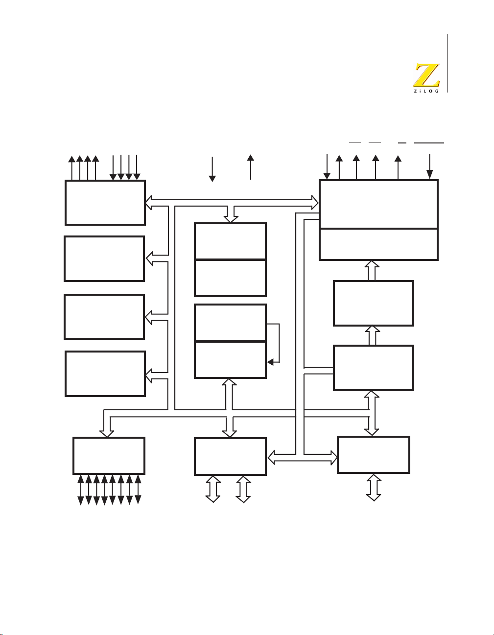
A generalized Z8 CPU® block diagram is shown in Figure 1. The same
on-chip peripherals are used across the MCU product line with the primary differences being the amount of ROM/RAM, number of I/O lines
present, and packaging/temperature ranges available. This allows code
written for one MCU device to be easily ported to another family member.
Z8 CPU
User Manual
1
Key Features
General-Purpose Register File. Every RAM register acts like an accumulator, speeding instruction execution and maximizing coding efficiency. Working register groups allow fast context switching.
Flexible I/O. I/O byte, nibble, and/or bit programmable as inputs or outputs. Outputs are software programmable as open-drain or push–pull on a
port basis. Inputs are Schmitt-triggered with autolatches to hold unused
inputs at a known voltage state.
Analog Inputs. Three input pins are software programmable as digital or
analog inputs. When in analog mode, two comparator inputs are provided
with a common reference input. These inputs are ideal for a variety of
common functions, including threshold level detection, analog-to-digital
UM001602-0904 Z8 CPU Product Overview
Page 20

Z8 Family of Microcontrollers
User Manual
2
conversion, and short circuit detection. Each analog input provides a
unique maskable interrupt input.
Timer/Counter. The Timer/Counter (T/C) consists of a programmable 6bit prescaler and 8-bit downcounter, with maskable interrupt upon end-ofcount. Software controls T/C load/start/stop, countdown read (at any time
on the fly), and maskable end-of-count interrupt. Special functions available include TIN (external counter input, external gate input, or external
trigger input) and T
system clock.) These special functions allow accurate hardware input
pulse measurement and output waveform generation.
Interrupts. There are six vectored interrupt sources with software-programmable enable and priority for each of the six sources.
Watch–Dog Timer. An internal Watch–Dog Timer (WDT) circuit is
included as a fail-safe mechanism so that if software strays outside the
bounds of normal operation, the WDT will time-out and reset the MCU.
To maximize circuit robustness and reliability, the default WDT clock
source is an internal RC circuit (isolated from the device clock source).
(external access to timer output or the internal
OUT
Auto Reset/Low-Voltage Protection. All family devices have internal
Power-On Reset. ROM devices add low-voltage protection. Low-voltage
protection ensures the MCU is in a known state at all times (in active
RUN mode or RESET) without external hardware (or a device reset pin).
Low-EMI Operation. Mode is programmable via software or as a mask
option. This new option provides for reduced radiated emission via clock
and output drive circuit changes.
Low-Power. CMOS with two standby modes; STOP and HALT.
Full Z8 Instruction Set. Forty-eight basic instructions, supported by six
addressing modes with the ability to operate on bits, nibbles, bytes, and
words.
Z8 CPU Product Overview UM001602-0904
Page 21
Z8 CPU
User Manual
3
Output
Port 3
Counter/
Timers (2)
Interrupt
Control
Analog
Comparators
(2)
Input
V
CC
Register File
256 x 8-Bit
GND
ALU
FLAG
Register
Pointer
XTAL
AS DS
Machine Timing
& Instruction Control
RESET, WDT,
POR
Prg. Memory
512/K x 8-Bit
Program
Counter
R/W RESET
Port 2
I/O
(Bit Programmable)
Port 0
4 4
Address or I/O
(Nibble Programmable)
Port 1
8
Address/Data or I/O
(Byte Programmable)
Figure 1. Z8 CPU Block Diagram
UM001602-0904 Z8 CPU Product Overview
Page 22

Z8 Family of Microcontrollers
User Manual
4
Product Development Support
The Z8® MCU product line is fully supported with a range of cross
assemblers, C compilers, ICEBOX emulators, single and gang OTP/
EPROM programmers, and software simulators.
The Z86CCP01ZEM low-cost Z8 CCP™ real-time emulator/programmer
kit was designed specifically to support all of the products outlined in
Table 1.
Table 1. ZiLOG General-Purpose Microcontroller Product Family
ROM/
Product
Z86C03 512/60 14 1 2 6 F Y Y Y 8 18
Z86E03 512/60 14 1 2 6 F Y N Y 8 18
Z86C04 1K/124 14 2 2 6 F Y Y Y 8 18
Z86E04 1K/124 14 2 2 6 F Y N Y 8 18
Z86C06 1K/124 14 2 2 6 P Y Y Y 12 18
Z86E06 1K/124 14 2 2 6 P Y N Y 12 18
Z86C08 2K/124 14 2 2 6 F Y Y Y 12 18
Z86E08 2K/124 14 2 2 6 F Y N Y 12 18
Z86C30 4K/236 24 2 2 6 P Y Y Y 12 28
Z86E30 4K/236 24 2 2 6 P Y N Y 12 28
Z86C31 2K/124 24 2 2 6 P Y Y Y 8 28
Z86E31 2K/124 24 2 2 6 P Y N Y 8 28
Z86C40 4K/236 32 2 2 6 P Y Y Y 16 40/44
Z86E40 4K/236 32 2 2 6 P Y N Y 16 40/44
*Note: Z86Cxx signify ROM devices; 86xx signify EPROM devices; F = fixed; P = programmable
RAM I/0 T/C AN INT WDT POR V
BO
RC
Speed
(MHz)
Pin
Count
Z8 CPU Product Overview UM001602-0904
Page 23

Z8 CPU
User Manual
The Z86CCP01ZEM kit comes with:
•
Z8 CCP Evaluation Board
•
Z8 CCP Power Cable
•
ZiLOG Developer’s Studio (ZDS) CD-ROM , Including WindowsBased GUI Host Software
•
1999 ZiLOG Technical Library
•
Z8 CCP User Manual
A Z8 CCP Emulator Accessory Kit (Z8CCP00ZAC) is also available and
provides an RS-232 cable and power cable along with the 28- and 40- pin
ZIF sockets and 28- and 40- pin target connector cables required to emulate/program 28/40 pin devices.
5
UM001602-0904 Z8 CPU Product Overview
Page 24

Z8 Family of Microcontrollers
User Manual
6
Z8 CPU Product Overview UM001602-0904
Page 25

Address Space
Introduction
Four address spaces are available for the Z8® CPU:
•
The Z8® Standard Register File contains addresses for peripheral,
control, all general-purpose, and all I/O port registers. This is the
default register file specification.
•
The Z8
trol and data registers for additional peripherals/features.
•
Z8 external program memory contains addresses for all memory locations having executable code and/or data.
®
Expanded Register File (ERF) contains addresses for con-
Z8 CPU
User Manual
7
•
Z8 external data memory contains addresses for all memory locations
that hold data only, whether internal or external.
Z8 CPU Standard Register File
The Z8
ters). The register file consists of 4 I/O ports (00h–03h), 236 GeneralPurpose Registers (04h–EFh), and 16 control registers (F0h–FFh).
Table 2 shows the layout of the register file, including register names,
locations, and identifiers.
Table 2. Z8 Standard Register File
UM001602-0904 Address Space
®
Standard Register File totals up to 256 consecutive bytes (Regis-
Hex Address Register Identifier Register Description
FF SPL Stack Pointer Low Byte
FE SPH Stack Pointer High Byte
FD RP Register Pointer
Page 26

Z8 Family of Microcontrollers
User Manual
8
Table 2. Z8 Standard Register File (Continued)
Hex Address Register Identifier Register Description
FC FLAGS Program Control Flags
FB IMR Interrupt Mask Register
FA IRQ Interrupt Request Register
F9 IPR Interrupt Priority Register
F8 P01M Port 0–1 Mode Register
F7 P3M Port 3 Mode Register
F6 P2M Port 2 Mode Register
F5 PRE0 T0 Prescaler
F4 T0 Timer/Counter 0
F3 PRE1 T1 Prescaler
F2 T1 Timer/Counter 1
F1 TMR Timer Mode
F0 SIO Serial I/O
EF R239
General-Purpose Registers (GPR)
04 R4
03 P3 Port 3
02 P2 Port 2
01 P1 Port 1
00 P0 Port 0
Registers can be accessed as either 8-bit or 16-bit registers using Direct,
Indirect, or Indexed Addressing. All 236 general-purpose registers can be
Address Space UM001602-0904
Page 27
Z8 CPU
User Manual
referenced or modified by any instruction that accesses an 8-bit register,
without the requirement for special instructions. Registers accessed as 16
bits are treated as even-odd register pairs (there are 118 valid pairs). In
this case, the data’s Most Significant Byte (MSB) is stored in the even
numbered register, while the Least Significant Byte (LSB) goes into the
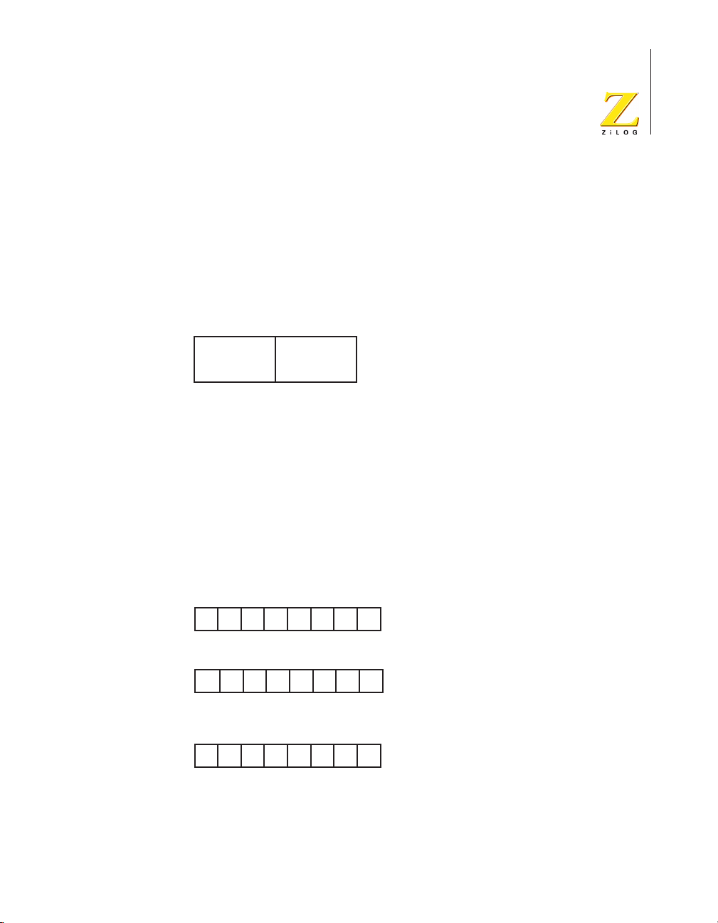
next higher odd numbered register. See Figure 2.
9
MSB
Rn Rn+1
n = Even Address
Figure 2. 16-Bit Register Addressing
LSB
By using a logical instruction and a mask, individual bits within registers
can be accessed for bit set, bit clear, bit complement, or bit test operations. For example, the instruction AND R15, MASK performs a bit clear
operation. Figure 3 shows this example.
0 1 1 1 0 0 0 0
1 1 0 1 1 1 1 1
AND R15, DFh ;Clear Bit 5 of Working Register 15
0 1 0 1 0 0 0 0
R15
MASK
R15
Figure 3. Accessing Individual Bits (Example)
UM001602-0904 Address Space
Page 28

Z8 Family of Microcontrollers
User Manual
10
When instructions are executed, registers are read when defined as
sources and written when defined as destinations. All General-Purpose
Registers function as accumulators, address pointers, index registers,
stack areas, or scratch pad memory.
General-Purpose Registers
General-Purpose Registers (GPR) are undefined after the device is powered up. The registers keep their last value after any reset, as long as the
reset occurs in the VCC voltage-specified operating range. It will not keep
its last state from a VLV reset if VCC drops below 1.8v.
Note:
Registers in Bank E0-EF may only be accessed through the working register and indirect addressing modes. Direct access cannot be used because
the 4-bit working register address mode already uses the format [E | dst],
where dst represents the working register number from 0h to Fh.
RAM Protect
The upper portion of the register file address space 80h to EFh (excluding
the control registers) may be protected from reading and writing. The
RAM Protect bit option is mask-programmable and is selected by the customer when the ROM code is submitted. After the mask option is
selected, the user activates this feature from the internal ROM code to
turn off/on the RAM Protect by loading either a 0 or 1 into the IMR register, bit D6. A 1 in D6 enables RAM Protect. Only devices that use registers 80h to EFh offer this feature.
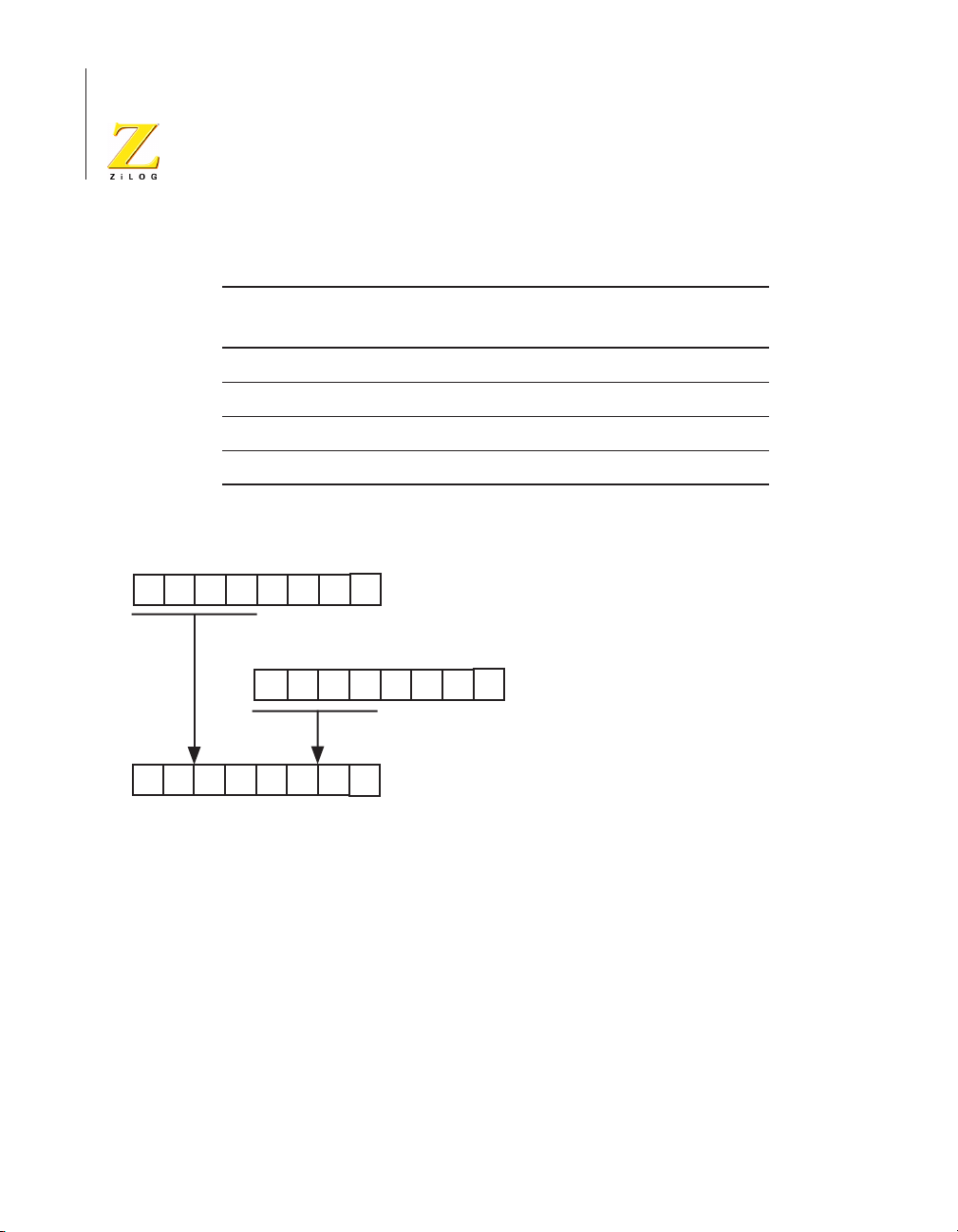
Working Register Groups
Z8 instructions can access 8-bit registers and register pairs (16-bit words)
using either 4-bit or 8-bit address fields. 8-bit address fields refer to the
actual address of the register. For example, Register 58h is accessed by
calling upon its 8-bit binary equivalent, 01011000 (58h).
With 4-bit addressing, the register file is logically divided into 16 Working Register Groups of 16 registers each, as shown in Table 3. These 16
Address Space UM001602-0904
Page 29

Z8 CPU
User Manual
registers are known as Working Registers. A Register Pointer (one of the
control registers, FDh) contains the base address of the active Working
Register Group. The high nibble of the Register Pointer determines the
current Working Register Group.
When accessing one of the Working Registers, the 4-bit address of the
Working Register is combined within the upper four bits (high nibble) of
the Register Pointer, thus forming the 8-bit actual address. Figure 4 illustrates this operation. Because working registers are typically specified by
short format instructions, there are fewer bytes of code required, which
reduces execution time. In addition, when processing interrupts or changing tasks, the Register Pointer speeds context switching. A special Set
Register Pointer (SRP) instruction sets the contents of the Register
Pointer.
Table 3. Working Register Groups
11
Register Pointer
(FDh) High Nibble
1111b F F0–FF
1110b E E0–EF
1101b D D0–DF
1100b C C0–CF
1011b B B0–BF
1010b A A0–AF
1001b 9 90–9F
1000b 8 80–8F
0111b 7 70–7F
0110b 6 60–6F
0101b 5 50–5F
0100b 4 40–4F
UM001602-0904 Address Space
Working Register
Group (Hex)
Actual Registers
(Hex)
Page 30
Z8 Family of Microcontrollers
User Manual
12
Table 3. Working Register Groups (Continued)
Register Pointer
(FDh) High Nibble
0011b 3 30–3F
0010b 2 20–2F
0001b 1 10–1F
0000b 0 00–0F
0 1 1 1 0 0 0 0
1 1 0 1 1 1 1 1
0 1 1 1 0 1 1 0
Figure 4. Working Register Addressing Examples
Working Register
Group (Hex)
Register Pointer (FDh), Standard Register File
INC R6 (instruction, short format)
Actual register address (76h)
Actual Registers
(Hex)
Address Space UM001602-0904
Page 31

Z8 CPU
User Manual
13
R7 R6 R5 R4 R3 R2 R1 R0
The upper nibble of the register file address,
provided by the register pointer, specifies
the active working-register group.
FF
F0
EF
80
7F
70
6F
60
5F
50
4F
40
3F
30
2F
20
1F
10
0F
00
*Note: The full register file is shown. Please refer to the selected device product specification for actual file size.
Working Register Group F
Specified Working Register Group
Working Register Group 1
Working Register Group 0
I/O Ports
R253
(Register Pointer)
The lower nibble
of the register
file address
(provided by the
instruction) points
to the specified
register.
R15 to R0
R15 to R4
R3 to R0
Figure 5. Register Pointer
Error Conditions
Registers in the Z8
because certain conditions produce inconsistent results and should be
avoided.
•
Registers F3h and F5h–F9h are write-only registers. If an attempt is
made to read these registers, FFh is returned. Reading any write-only
register will return FFh.
UM001602-0904 Address Space
®
Standard Register File must be correctly used
Page 32

Z8 Family of Microcontrollers
User Manual
14
•
•
•
•
•
When register FDh (Register Pointer) is read, the least significant four
bits (lower nibble) will indicate the current Expanded Register File
Bank. (Example: 0000 indicates the Standard Register File, while
1010 indicates Expanded Register File Bank A.)
When Ports 0 and 1 are defined as address outputs, registers 00h and
01h will return 1s in each address bit location when read.
Writing to bits that are defined as timer output, serial output, or handshake output will have no effect.
The Z8® CPU instruction DJNZ uses any general-purpose working
register as a counter.
Logical instructions such as OR and AND require that the current
contents of the operand be read. They therefore will not function
properly on write-only registers.
•
The WDTMR register must be written within the first 60 internal system clocks (SCLK) of operation after a reset.
Z8 Expanded Register File
The standard register file of the Z8
Expanded Register File (ERF) Banks, as shown in Figure 6. Each ERF
Bank consists of up to 256 registers (the same amount as in the Standard
Register File) that can then be divided into 16 Working Register Groups.
This expansion allows for access to additional feature/peripheral control
and data registers.
Address Space UM001602-0904
®
CPU has been expanded to form 16
Page 33

Working Register
Group Pointer
Z8 Register File
FF
F0
7F
0F
00
Register Pointer
D7 D6 D5 D4 D3 D2 D1 D0
Expanded Register
Group Pointer
Expanded Register File
Bank (F)
(F) 0F WDTMR
(F) 0E Reserved
(F) 0E Reserved
(F) 0D Reserved
(F) 0C Reserved
(F) 0B SMR
(F) 0A Reserved
(F) 09 Reserved
(F) 08 Reserved
(F) 07 Reserved
(F) 06 Reserved
(F) 05 Reserved
(F) 04 Reserved
(F) 03 Reserved
(F) 02 Reserved
(F) 01 Reserved
(F) 00 PCON
Expanded Register File
Bank (0)
(0) 0F GPR
(0) 0E GPR
(0) 0D GPR
(0) 0C GPR
(0) 0B GPR
(0) 0A GPR
(0) 09 GPR
(0) 08 GPR
(0) 07 GPR
(0) 06 GPR
(0) 05 GPR
(0) 04 GPR
(0) 03 P3
(0) 02 P2
(0) 01 P1
(0) 00 P0
User Manual
Expanded Register File
Bank (C)
(C) 0F Reserved
(C) 0E Reserved
(C) 0D Reserved
(C) 0C Reserved
(C) 0B Reserved
(C) 0A Reserved
(C) 09 Reserved
(C) 08 Reserved
(C) 07 Reserved
(C) 06 Reserved
(C) 05 Reserved
(C) 04 Reserved
(C) 03 Reserved
(C) 02 SCON
(C) 01 RXBUF
(C) 00 SCOMP
Z8 CPU
15
*Note: The fully implemented register file is shown. Please refer to the specific product specification for actual register file architecture implemented.
Figure 6. Expanded Register File Architecture
UM001602-0904 Address Space
Page 34

Z8 Family of Microcontrollers
User Manual
16
Currently, three out of the possible sixteen Z8 ERF Banks have been
implemented. ERF Bank 0, also known as the Z8® Standard Register File,
has all 256 bytes defined, as shown in Figure 7. Only Working Register
Group 0 (register addresses 00h to 0Fh) have been defined for ERF Bank
C and ERF Bank F (see Table 4). All other working register groups in
ERF Banks C and F, as well as the remaining thirteen ERF Banks, are not
implemented. All are reserved for future use.
When an ERF Bank is selected, register addresses 00h to 0Fh access
those sixteen ERF Bank registers—in effect replacing the first sixteen
locations of the Z8® Standard Register File.
For example, if ERF Bank C is selected, the Z8® Standard Registers 00h
through 0Fh are no longer accessible. Registers 00h through 0Fh are now
the 16 registers from ERF Bank C, Working Register Group 0. No other
Z8 Standard Registers are affected because only Working Register Group
0 is implemented in ERF Bank C.
Access to the ERF is accomplished through the Register Pointer (FDh).
The lower nibble of the Register Pointer determines the ERF Bank while
the upper nibble determines the Working Register Group within the register file, as Figure 7 shows.
0 1 1 1
Working
Register
Group
Select ERF Bank Ch
Working Register Group 7h
Figure 7. Register Pointer Example
Address Space UM001602-0904
1 1 0 0
Expanded
Register
Bank
Page 35

Z8 CPU
User Manual
The value of the lower nibble in the Register Pointer (FDh) corresponds to
the ERF Bank identification. Table 4 shows the lower nibble value and the
register file assigned to it.
Table 4. ERF Bank Address
Register
Pointer (FDh)
Low Nibble
0000b 0 Z8 Standard Register File.*
0001b 1 Expanded Register File Bank 1.
0010b 2 Expanded Register File Bank 2.
0011b 3 Expanded Register File Bank 3..
0100b 4 Expanded Register File Bank 4
Hex
Register File
17
0101b 5 Expanded Register File Bank 5..
0110b 6 Expanded Register File Bank 6
0111b 7 Expanded Register File Bank 7..
1000b 8 Expanded Register File Bank 8
1001b 9 Expanded Register File Bank 9..
1010b A Expanded Register File Bank A
1011b B Expanded Register File Bank B.
1100b C Expanded Register File Bank C.
1101b D Expanded Register File Bank D..
1110b E Expanded Register File Bank E
1111b F Expanded Register File Bank F.
*Note: the Z8® Standard Register File is equivalent to Expanded Register File Bank 0.
UM001602-0904 Address Space
Page 36

Z8 Family of Microcontrollers
User Manual
18
The upper nibble of the register pointer selects which group of 16 bytes in
the Register File, out of the 256 total bytes, will be accessed as working
registers. Table 5 shows an example.
Table 5. Register Pointer Access Example
R253 RP = 00h ;ERF Bank 0, Working Reg. Group 0.
R0 = Port 0 = 00h
R1 = Port 1 = 01h
R2 = Port 2 = 02h
R3 = Port 3 = 03h
R11 = GPR 0Bh
R15 = GPR 0Fh
If R253 RP = 0Fh ;ERF Bank F, Working Reg. Group 0.
R0 = PCON = 00h
R1 = Reserved = 01h
R2 = Reserved = 02h
R11 = SMR = 0Bh
R15 = WDTMR = 0Fh
Address Space UM001602-0904
Page 37

Table 5. Register Pointer Access Example (Continued)
If R253 RP = FFh
;ERF Bank F, Working Reg. Group F.
00h = PCON
R0 = SI0 01h = Reserved
R1 = TMR 02h = Reserved
...
R2 = T1 0Bh = SMR
...
R15 = SPL 0Fh = WDTMR
Z8 CPU
User Manual
19
Because enabling an ERF Bank (C or F) only changes register addresses
00h to 0Fh, the working register pointer can be used to access either the
selected ERF Bank (Bank C or F, Working Register Group 0) or the Z8
®
Standard Register File (ERF Bank 0, Working Register Groups 1 through
F).
When an ERF Bank other than Bank 0 is enabled, the first 16 bytes of the
Z8® Standard Register File (I/O ports 0 to 3, Groups 4 to F) are no longer
accessible (the selected ERF Bank, Registers 00h to 0Fh are accessed
instead). It is important to re-initialize the Register Pointer to enable ERF
Bank 0 when these registers are required for use.
The SPI register is mapped into ERF Bank C. Access is easily done using
the example in Table 6.
UM001602-0904 Address Space
Page 38

Z8 Family of Microcontrollers
User Manual
20
Table 6. ERF Bank C Access Example
LD RP, #0Ch ;Select ERF Bank C working
LD R2,#xx ;access SCON
LD R1, #xx ;access RXBUF
LD RP, #00h ;Select ERF Bank 0 so I/O ports
Table 7. Z8 Expanded Register File Bank Layout
Expanded Register
File Bank ERF
;register group 0 for access.
;are again accessible.
Fh PCON, SMR, WDT, (00h, 0Bh, 0Fh),
Working Register Group 0 only
implemented.
Eh Not implemented (reserved)
Dh Not implemented (reserved)
Ch SPI Registers: SCOMP, RXBUF, SCON
(00h, 01h, 02h), Working Register Group 0
only implemented.
Bh Not implemented (reserved)
Ah Not implemented (reserved)
9h Not implemented (reserved)
8h Not implemented (reserved)
7h Not implemented (reserved)
6h Not implemented (reserved)
5h Not implemented (reserved)
Address Space UM001602-0904
Page 39

Z8 CPU
User Manual
Table 7. Z8 Expanded Register File Bank Layout
Expanded Register
File Bank ERF
4h Not implemented (reserved)
3h Not implemented (reserved)
2h Not implemented (reserved)
1h Not implemented (reserved)
0h Z8 Ports 0, 1, 2, 3, and General-Purpose
Registers 04h to EFh, and control
registers F0h to FFh.
Please refer to the specific product specification to determine the above
registers are implemented.
21
Z8 Control and Peripheral Registers
Standard Z8 Registers
The standard Z8 control registers govern the operation of the CPU. Any
instruction which references the register file can access these control registers. Available control registers are:
•
Interrupt Priority Register (IPR)
•
Interrupt Mask Register (IMR)
•
Interrupt Request Register (IRQ)
•
Program Control Flags (FLAGS)
•
Register Pointer (RP)
•
Stack Pointer High-Byte (SPH)
•
Stack Pointer Low-Byte (SPL)
UM001602-0904 Address Space
Page 40

Z8 Family of Microcontrollers
User Manual
22
The Z8® CPU uses a 16-bit Program Counter (PC) to determine the
sequence of current program instructions. The PC is not an addressable
register.
Peripheral registers are used to transfer data, configure the operating
mode, and control the operation of the on-chip peripherals. Any instruction that references the register file can access the peripheral registers.
The peripheral registers are:
•
•
•
•
•
Serial I/O (SIO)
Timer Mode (TMR)
Timer/Counter 0 (T0)
T0 Prescaler (PRE0)
Timer/Counter 1 (T1)
•
T1 Prescaler (PRE1)
•
Port 0–1 Mode (P01M)
•
Port 2 Mode (P2M)
•
Port 3 Mode (P3M)
In addition, the four port registers (P0–P3) are considered to be peripheral
registers.
Expanded Z8 Registers
The expanded Z8 control registers govern the operation of additional features or peripherals. Any instruction which references the register file can
access these registers.
The ERF contains the control registers for WDT, Port Control, Serial
Peripheral Interface (SPI), and the SMR functions. Figure 6 on page 15
shows the layout of the Register Banks in the ERF. Register Bank C in the
ERF consists of the registers for the SPI. Table 8 shows the registers
within ERF Bank C, Working Register Group 0.
Address Space UM001602-0904
Page 41

Table 8. Expanded Register File Register Bank C
WR Group 0
Working
Register Function
F Reserved R15
E Reserved R14
D Reserved R13
C Reserved R12
B Reserved R11
A Reserved R10
9 Reserved R9
8 Reserved R8
Register
Z8 CPU
User Manual
23
7 Reserved R7
6 Reserved R6
5 Reserved R5
4 Reserved R4
3 Reserved R3
2 SPI Control (SCON) R2
1 SPI Tx/Rx Data (Roxburgh) R1
0 SPI Compare (SCOMP) R0
UM001602-0904 Address Space
Page 42

Z8 Family of Microcontrollers
User Manual
24
Working Register Group 0 in ERF Bank 0 consists of the registers for Z8
General-Purpose Registers and ports. Table 9 shows the registers within
this group.
Table 9. Expanded Register File Bank 0
WR Group 0
Register Function
F General-Purpose Register R15
E General-Purpose Register R14
D General-Purpose Register R13
C General-Purpose Register R12
B General-Purpose Register R11
Working
Register
A General-Purpose Register R10
9 General-Purpose Register R9
8 General-Purpose Register R8
7 General-Purpose Register R7
6 General-Purpose Register R6
5 General-Purpose Register R5
4 General-Purpose Register R4
3 Port 3 R3
2 Port 2 R2
1 Port 1 R1
0 Port 0 R0
Address Space UM001602-0904
Page 43

Z8 CPU
User Manual
Working Register Group 0 in ERF Bank F consists of the control registers
for STOP mode, WDT, and port control. Table 10 shows the registers
within this group.
Table 10. Expanded Register File Bank F
WR Group 0
Working
Register Function
F WDTMR R15
E Reserved R14
D Reserved R13
C Reserved R12
B SMR R11
Register
25
A Reserved R10
9 Reserved R9
8 Reserved R8
7 Reserved R7
6 Reserved R6
5 Reserved R5
4 Reserved R4
3 Reserved R3
2 Reserved R2
1 Reserved R1
0 PCON R0
UM001602-0904 Address Space
Page 44

Z8 Family of Microcontrollers
User Manual
26
The functions and applications of the control and peripheral registers are
described in subsequent sections of this manual.
Program Memory
The first 12 bytes of program memory are reserved for the interrupt vectors, as shown in Figure 8. These locations contain six 16-bit vectors that
correspond to the six available interrupts. Address 12 up to the maximum
ROM address consists of on-chip mask-programmable ROM. See the
product data sheet for the exact program, data, register memory size, and
address range available. At addresses outside the internal ROM, the Z8®
CPU executes external program memory fetches through Port 0 and Port
1 in Address/Data mode for devices with Port 0 and Port 1 featured. Otherwise, the program counter will continue to execute NOPs up to address
FFFFh, roll over to 0000h, and continue to fetch executable code (see
Figure 8).
The internal program memory is one-time programmable (OTP) or mask
programmable dependent on the specific device. A ROM protect feature
prevents dumping of the ROM contents by inhibiting execution of the
LDC, LDCI, LDE, and LDEI instructions to program memory in all
modes. ROM look-up tables cannot be used with this feature.
The ROM Protect option is mask-programmable, to be selected by the
customer when the ROM code is submitted. For the OTP ROM, the ROM
Protect option is an OTP programming option.
Address Space UM001602-0904
Page 45

Location of
First Byte of
Instruction
Executed
After RESET
65535
4096
4095
12
External
ROM and RAM
On–Chip
ROM
Z8 CPU
User Manual
27
Interrupt
Vector
(Lower Byte)
Interrupt
Vector
(Upper Byte)
Figure 8. Z8 Program Memory Map
Z8 External Memory
The Z8® CPU, in some cases, has the capability to access external program memory with the 16-bit Program Counter. To access external pro-
11
10
9
8
7
6
5
4
3
2
1
0
IRQ
IRQ
IRQ
IRQ
IRQ
IRQ
IRQ
IRQ
IRQ
IRQ
IRQ
IRQ
5
5
4
4
3
3
2
2
1
1
0
0
UM001602-0904 Address Space
Page 46

Z8 Family of Microcontrollers
User Manual
28
gram memory the Z8® CPU offers multiplexed address/data lines (AD7–
AD0) on Port 1 and address lines (A15–A8) on Port 0. This feature only
applies to devices that offer Port 0 and Port 1. The maximum external
address is FFFF. This memory interface is supported by the control lines
AS (Address Strobe), DS (Data Strobe), and R/W (Read/Write). The origin of the external program memory starts after the last address of the
internal ROM. Figure 9 shows an example of external program memory
for the Z8® CPU.
External Data Memory
The Z8® CPU, in some cases, can address up to 60 KB of external data
memory beginning at location 4096. External data memory (DM) can be
included with, or separated from, the external program memory space.
DM, an optional I/O function that can be programmed to appear on pin
P34, is used to distinguish between data and program memory space. The
state of the DM signal is controlled by the type of instruction being executed. An LDC opcode references program memory (DM inactive) , and
an LDE instruction references data memory (DM active Low) . The user
must configure Port 3 Mode Register (P3M) bits D3 and D4 for this
mode.
Address Space UM001602-0904
Page 47

65535
External
Memory
Z8 CPU
User Manual
29
4096
4095
Not Addressable
0
*Note: For additional information on using external memory, see Chapter 10 of this manual. For exact
memory addressing options available, see the device product specification.
Figure 9. External Memory Map
UM001602-0904 Address Space
Page 48

Z8 Family of Microcontrollers
User Manual
30
Z8 Stacks
Stack operations can occur in either the Z8® Standard Register File or
external data memory. Under software control, Port 0–1 Mode register
(F8h) selects the stack location. Only the General-Purpose Registers can
be used for the stack when the internal stack is selected.
The register pair FEh and FFh form the 16-bit Stack Pointer (SP), that is
used for all stack operations. The stack address is stored with the MSB in
FEh and LSB in FFh; see Figure 10.
FFh
LOWER Byte
Stack Pointer Low
FEh
Figure 10. Stack Pointer
UPPER Byte
Stack Pointer High
The stack address is decremented prior to a PUSH operation and incremented after a POP operation. The stack address always points to the data
stored on the top of the stack. The Z8® CPU stack is a return stack for
CALL instructions and interrupts, as well as a data stack.
During a CALL instruction, the contents of the PC are saved on the stack.
The PC is restored during a RETURN instruction. Interrupts cause the
contents of the PC and Flag registers to be saved on the stack. The IRET
instruction restores them Figure 11.
When the Z8® CPU is configured for an internal stack (using the Z8®
Standard Register File), register FFh serves as the Stack Pointer. The
Address Space UM001602-0904
Page 49

Z8 CPU
User Manual
value in FEh is ignored. FEh can be used as a general-purpose register in
this case only.
An overflow or underflow can occur when the stack address is incremented or decremented during normal stack operations. The programmer
must prevent this occurrence or unpredictable operation will result.
PCL
31
Top of Stack
PCL
PCH
Stack Contents
After a Call
Instruction
Top of Stack
Figure 11. Stack Operations
PCH
FLAGS
Stack Contents
After an
Interrupt Cycle
UM001602-0904 Address Space
Page 50

Z8 Family of Microcontrollers
User Manual
32
Address Space UM001602-0904
Page 51

Clock
Frequency Control
Z8 CPU
User Manual
33
The Z8® CPU derives its timing from on-board clock circuitry connected
to pins XTAL1 and XTAL2. The clock circuitry consists of an oscillator, a
divide-by-two shaping circuit, and a clock buffer. Figure 12 illustrates the
clock circuitry. The oscillator’s input is XTAL1 and its output is XTAL2.
The clock can be driven by a crystal, a ceramic resonator, LC clock, RC,
or an external clock source.
In some cases, the Z8® CPU has an EPROM/OTP option or a Mask ROM
option bit to bypass the divide-by-two flip flop in Figure 12. This feature
is used in conjunction with the low EMI option. When low EMI is
selected, the device output drive and oscillator drive is reduced to approximately 25 percent of the standard drive and the divide-by-two flip flop is
bypassed such that the XTAL clock frequency is equal to the internal system clock frequency. In this mode, the maximum frequency of the XTAL
clock is 4 MHz. Please refer to specific product specification for availability of options and output drive characteristics.
XTAL1
OSC
XTAL2
Figure 12. Z8® CPU Clock Circuit
÷2
Buffer
Internal
Clock
Clock Control
In some cases, the Z8® CPU offers software control of the internal system
clock via programming register bits. The bits are located in the StopMode Recovery Register in Expanded Register File Bank F, Register 0Bh.
UM001602-0904 Clock
Page 52

Z8 Family of Microcontrollers
User Manual
34
This register selects the clock divide value and determines the mode of
Stop-Mode Recovery (see Figure 13). Please refer to the specific product
specification for availability of this feature/register.
SMR (F) OB
D7 D6 D5 D4 D3 D2 D1 D0
SCLK ÷ TCLK D ivide by 16
0 OFF **
1 ON
External Clock Divide Mode by 2
0 = SCLK
* Default setting after RESET.
**Default setting after RESET and Stop-Mode R ecovery.
1 = SCLK
Figure 13. Stop-Mode Recovery Register (Write-Only Except D7,
Which is Read-Only)
SCLK ÷ TCLK Divide-By-16 Select
The D0 bit of the SMR controls a divide-by-16 prescaler of
SCLK ÷ TCLK. The purpose of this control is to selectively reduce
device power consumption during normal processor execution (SCLK
control) and/or HALT mode (where TCLK sources counter/timers and
interrupt logic).
External Clock Divide-By-Two
The D1 bit can eliminate the oscillator divide-by-two circuitry. When this
bit is 0, SCLK (System Clock) and TCLK (Timer Clock) are equal to the
external clock frequency divided by two. The SCLK ÷ TCLK is equal to
the external clock frequency when this bit is set (D1 = 1). Using this bit,
together with D7 of PCON, further helps lower EMI (D7 (PCON) = 0, D1
(SMR) = 1). The default setting is 0. Maximum frequency is 4 MHz with
D1 = 1 (see Figure 14).
÷
TCLK = XTAL
÷
TCLK = X TAL
2*
÷
Clock UM001602-0904
Page 53

D1 (SMR)
D0 (SMR)
OSC
÷2
Z8 CPU
User Manual
35
Figure 14. External Cloc k Cir cuit
Oscillator Contr ol
In some cases, the Z8
select lo w EMI dri v e or standard dri v e. The selection is done by program ming bit D7 of the Port Confi guration (PCON) re gister ( see Figure 15 ) .
The PCON re gister is located in Expanded Re gister File Bank F , Re gister
00h
UM001602-0904
External Clock
.
÷16
®
CPU of fers softw are control of the oscillator to
Clock
Page 54

Z8 Family of Microcontrollers
User Manual
36
A 1 in bit D7 confi
fi
gures the oscillator with Lo
capability of the oscillator and does not affect the relationship of the
XTAL clock frequency to the internal system clock (SCLK).
PCON (Fh) 00h
D7 D6 D5 D4 D3 D2 D1 D0
Figure 15. Port Configuration Register (Write-Only)
Oscillator Operation
The Z8® CPU uses a Pierce oscillator with an internal feedback (see
Figure 16). The advantages of this circuit are low cost, large output signal,
low-power level in the crystal, stability with respect to VCC and temperature, and low impedances (not disturbed by stray affects).
One drawback is the requirement for high gain in the amplifier to compensate for feedback path losses. The oscillator amplifies its own noise at
start-up until it settles at the frequency that satisfies the gain/phase
requirements A x B = 1, where A = V0/VI is the gain of the amplifier and
B = VI/V0 is the gain of the feedback element. The total phase shift
around the loop is forced to zero (360 degrees). Because VIN must be in
phase with itself, the amplifier/inverter provides 180 degree phase shift
and the feedback element is forced to provide the other 180 degrees of
phase shift.
gures the oscillator with standard drive, while a 0 con
w EMI dri
ve. This only affects the drive
Low EMI Oscillator
0 Low EMI
1 Standard
-
Clock
R1 is a resistive component placed from output to input of the amplifier.
The purpose of this feedback is to bias the amplifier in its linear region
and to provide the start-up transition.
UM001602-0904
Page 55

Z8 CPU
User Manual
Capacitor C2 combined with the amplifier output resistance provides a
small phase shift. It will also provide some attenuation of overtones.
Capacitor C1 combined with the crystal resistance provides additional
phase shift.
C1 and C2 can affect the start-up time if they increase dramatically in size.
As C1 and C2 increase, the start-up time increases until the oscillator
reaches a point where it does not start up any more.
For fast and reliable oscillator start-up over the manufacturing process
range, ZiLOG recommends that the load capacitors be sized as low as
possible without resulting in overtone operation.
37
Layout
XTAL1
Z8 CPU
A
RI
V
1
C1
V
0
XTAL2
C2
V
SS
Figure 16. Pierce Oscillator with Internal Feedback Circuit
Traces connecting crystal, caps, and the Z8® CPU oscillator pins should
be as short and wide as possible. This reduces parasitic inductance and
resistance. The components (caps, crystal, resistors) should be placed as
close as possible to the oscillator pins of the Z8® CPU .
The traces from the oscillator pins of the IC and the ground side of the
lead caps should be guarded from all other traces (clock, VCC, address/
UM001602-0904 Clock
Page 56

Z8 Family of Microcontrollers
User Manual
38
data lines, system ground) to reduce cross talk and noise injection. This is
usually accomplished by keeping other traces and system ground trace
planes away from the oscillator circuit and by placing a Z8® CPU device
VSS ground ring around the traces/components. The ground side of the
oscillator lead caps should be connected to a single trace to the Z8®
CPU’s VSS (GND) pin. It should not be shared with any other system
ground trace or components except at the Z8® CPU’s VSS pin. This is to
prevent differential system ground noise injection into the oscillator (see
Figure 17).
Indications of an Unreliable Design
Start-up time and output level are two major indicators that are used in
working designs to determine their reliability over full lot and temperature variations. These two indicators are described below.
Start-Up Time. If start-up time is excessive, or varies widely from unit to
unit, there is probably a gain problem. C1/C2 must be reduced; the amplifier gain is not adequate at frequency, or crystal resistance is too large.
Output Level. The signal at the amplifier output should swing from
ground to VCC. This indicates there is adequate gain in the amplifier. As
the oscillator starts up, the signal amplitude grows until clipping occurs,
at which point the loop gain is effectively reduced to unity and constant
oscillation is achieved. A signal of less than 2.5 volts peak-to-peak is an
indication that low gain may be a problem. Either C1 or C2 should be
made smaller or a low-resistance crystal should be used.
Circuit Board Design Rules
The following circuit board design rules are suggested:
•
To prevent induced noise the crystal and load capacitors should be
physically located as close to the Z8® CPU as possible.
Clock UM001602-0904
Page 57

Z8 CPU
User Manual
•
Signal lines should not run parallel to the clock oscillator inputs. In
particular, the crystal input circuitry and the internal system clock
output should be separated as much as possible.
•
VCC power lines should be separated from the clock oscillator input
circuitry.
•
Resistivity between XTAL1 or XTAL2 and the other pins should be
greater than 10 MΩ.
39
UM001602-0904 Clock
Page 58

Z8 Family of Microcontrollers
User Manual
40
C1
C2
XTAL1
Z8 CPU
XTAL2
V
SS
20 mm
max
Signal Line
Layout Should
Avoid High
Lighted Areas
Clock Generator Circuit
Signals A B
(Parallel Traces
Must Be Avoided)
Signal C
2
3
(Connection to System Group
Must Be Avoided)
Figure 17. Circuit Board Design Rules
Crystals and Resonators
Crystals and ceramic resonators, shown in Figure 18 should have the
characteristics listed in Table 11 to ensure proper oscillator operation.
Z8 CPU
1
2
3
Z8 CPU
V
SS
Board Design Example
(Top View)
Clock UM001602-0904
Page 59

Z8 CPU
User Manual
Table 11. Crystal/Resonator Characteristics
Crystal Cut: AT (crystal only)
Mode: Parallel, Fundamental mode
Crystal Capacitance: < 7 pF
Load Capacitance: 10 pF < CL < 220 pF, 15 typical
Resistance: 100 Ω max
Depending on operation frequency, the oscillator may require the addition
of capacitors C1 and C2 (shown in Figure 18). The capacitance values are
dependent on the manufacturer’s crystal specifications.
41
V
SS
XTAL2
R
C2
D
Z8 CPU
XTAL1
RF
C1
Figure 18. Crystal/Ceramic Resonator Oscillator
UM001602-0904 Clock
Page 60

Z8 Family of Microcontrollers
User Manual
42
C1
C2
Figure 19. LC Clock
In most cases, the RD is 0 Ω and RF is infinite. It is determined and specified by the crystal/ceramic resonator manufacturer. The RD can be
increased to decrease the amount of drive from the oscillator output to the
crystal. It can also be used as an adjustment to avoid clipping of the oscillator signal to reduce noise. The RF can be used to improve the start-up of
the crystal/ceramic resonator. The Z8® oscillator already has an internal
shunt resistor in parallel to the crystal/ceramic resonator.
L
XTAL1
Z8 CPU
XTAL2
V
SS
XTAL1
Z8 CPU
V
SS
XTAL2
Figure 20. External Clock
Clock UM001602-0904
Page 61

Z8 CPU
User Manual
In Figures 18 through 20, ZiLOG recommends that the user connect the
load capacitor ground trace directly to the VSS (GND) pin of the Z8®
CPU to ensure that no system noise is injected into the Z8® clock. This
trace should not be shared with any other components except at the VSS
pin of the Z8® CPU.
In some cases, the Z8® CPU’s XTAL1 pin also functions as one of the
EPROM high-voltage mode programming pins or as a special factory test
pin. In this case, applying 2 V above VCC on the XTAL1 pin will cause
the device to enter one of these modes. Because this pin accepts high voltages to enter these respective modes, the standard input protection diode
to VCC is not on XTAL1. ZiLOG recommends that in applications where
the Z8® CPU is exposed to much system noise, a diode from XTAL1 to
VCC be used to prevent accidental enabling of these modes. This diode
will not affect the crystal/ceramic resonator operation.
43
Please note that a parallel resonant crystal or resonator data sheet will
specify a load capacitor value that is the series combination of C1 and C2,
including all parasitics (PCB and holder).
LC Oscillator
The Z8® CPU oscillator can use a LC network to generate a XTAL clock
(see Figure 19).
The frequency stays stable over VCC and temperature. The oscillation frequency is determined by the equation.
Frequency =
where L is the total inductance including parasitics and CT is the total
series capacitance including the parasitics.
Simple series capacitance is calculated using the following equation:
UM001602-0904 Clock
1
2 π (LCT)
1/2
Page 62

Z8 Family of Microcontrollers
User Manual
44
1
CT C1 C
If C1 = C
1 = 2
CT = C
C1 = 2CT
Sample calculation of capacitance C1 and C2 for 5.83 MHz frequency and
inductance value of 27 µH.
5.83 (106) =
CT = 27.6 pF
Thus C1 = 55.2 pF and C2 = 55.2 pF.
RC Oscillator
In some cases, the Z8® CPU features an RC oscillator option. Please refer
to the specific product specification for availability. The RC oscillator
requires a resistor across XTAL1 and XTAL2. An additional load capacitor is required from the XTAL1 input to VSS pin (see Figure 21).
=
1
1
+
2
2
1
1
2π [2.7 (10–6) CT] 1/2
Clock UM001602-0904
Page 63

XTAL1
R
Z8 CPU
XTAL2
C1
Figure 21. RC Clock
Z8 CPU
User Manual
45
V
SS
UM001602-0904 Clock
Page 64

Z8 Family of Microcontrollers
User Manual
46
Clock UM001602-0904
Page 65

Reset
Z8 CPU
User Manual
47
This section describes the Z8® CPU reset conditions, reset timing, and
register initialization procedures. Reset is generated by Power-On Reset
(POR), Reset Pin, Watch–Dog Timer (WDT), and Stop-Mode Recovery.
A system reset overrides all other operating conditions and puts the Z8®
CPU into a known state. To initialize the chip’s internal logic, the RESET
input must be held Low for at least 21 SCP or 5 XTAL clock cycles. The
control register and ports are reset to their default conditions after a POR,
a reset from the RESET pin, or Watch–Dog Timer time-out while in RUN
mode and HALT mode. The control registers and ports are not reset to
their default conditions after Stop- Mode Recovery and WDT time-out
while in STOP mode.
While RESET pin is Low, AS is output at the internal clock rate, DS is
forced Low, and R/W remains High. The program counter is loaded with
000Ch. I/O ports and control registers are configured to their default reset
state.
Resetting the Z8® CPU does not affect the contents of the general-purpose registers.
Reset Pin, Internal POR Operation
In some cases, the Z8® CPU hardware RESET pin initializes the control
and peripheral registers, as shown in Tables 12 through 15. Specific reset
values are shown by 1 or 0, while bits whose states are unknown are indicated by the letter U. Tables 12 through 15 show the reset conditions for
the Z8 CPU.
Note:
UM001602-0904 Reset
The register file reset state is device dependent. Please refer to the selected
device product specifications for register availability and reset state.
Page 66

Z8 Family of Microcontrollers
User Manual
48
Table 12. Sample Control and Peripheral Register Reset Values (ERF Bank 0)
Register
(Hex) Register Name
F0 Serial I/O U U U U U U U U
F1 Timer Mode 0 0 0 0 0 0 0 0 Counter/Timers stopped.
F2 Counter/Timer1 U U U U U U U U
F3 T1 Prescaler U U U U U U 0 0 Single-pass count mode,
F4 Counter/Timer0 U U U U U U U U
F5 T0 Prescaler U U U U U U U 0 Single-pass count mode.
F6 Port 2 Mode 1 1 1 1 1 1 1 1 All inputs.
F7 Port 3 Mode 0 0 0 0 0 0 0 0 Port 2 open-drain, P33–
F8 Port 0–1 Mode 0 1 0 0 1 1 0 1 Internal Stack, Normal
F9 Interrupt Priority U U U U U U U U
FA Interrupt Request 0 0 0 0 0 0 0 0 All Interrupts Cleared.
FB Interrupt Mask 0 U U U U U U U Interrupts Disabled.
FC Flags U U U U U U U U
FD Register Pointer 0 0 0 0 0 0 0 0
FE Stack Pointer
(High)
FF Stack Pointer
(Low)
U U U U U U U U
U U U U U U U U
Bits
Comments7 6 5 4 3 2 1 0
external clock source.
P30 Input, P37–P34
Output.
Memory Timing.
Reset UM001602-0904
Page 67

Clock
SCLK
Z8 CPU
User Manual
49
Program execution starts 5 to 10 clock cycles after internal RESET has
returned High. The initial instruction fetch is from location 000Ch.
Figure 22 illustrates reset timing.
First Machine Cycle
T1
RESET
AS
DS
R/W
Hold Low For 4 SCLK
Periods (Minimum)
First Instruction Fetch
Figure 22. Reset Timing
After a reset, the first routine executed should be one that initializes the
control registers to the required system configuration.
The RESET pin is the input of a Schmitt-triggered circuit. Resetting the
Z8® CPU will initialize port and control registers to their default states.
To form the internal reset line, the output of the trigger is synchronized
with the internal clock. The clock must therefore be running for RESET
to function. It requires 4 internal system clocks after reset is detected for
the Z8® CPU to reset the internal circuitry. An internal pull-up, combined
with an external capacitor of 1 uf, provides enough time to properly reset
the Z8® CPU (see Figure 23). In some cases, the Z8® CPU has an internal
POR timer circuit that holds the Z8® CPU in reset mode for a duration
UM001602-0904 Reset
Page 68

Z8 Family of Microcontrollers
User Manual
50
(T
POR
internally generated reset drives the reset pin low for the POR time. Any
devices driving the reset line must be open-drained in order to avoid damage from possible conflict during reset conditions. This reset time allows
the on-board clock oscillator to stabilize.
To avoid asynchronous and noisy reset problems, the Z8® CPU is
equipped with a reset filter of four external clocks (4TpC). If the external
reset signal is less than 4TpC in duration, no reset occurs. On the fifth
clock after the reset is detected, an internal RST signal is latched and held
for an internal register count of 18 external clocks, or for the duration of
the external reset, whichever is longer. During the reset cycle, DS is held
active low while AS cycles at a rate of the internal system clock. Program
execution begins at location 000Ch, 5-10 TpC cycles after RESET is
released. For the internal Power-On Reset, the reset output time is specified as T
ues.
) before releasing the device out of reset. On these Z8 devices, the
. Please refer to specific product specifications for actual val-
POR
+5V
100 KΩ
RESET
1K
Figure 23. Example of External Power-On Reset Circuit
Reset UM001602-0904
1 µF
10 V
to
200 KΩ
Page 69

User Manual
Table 13. Expanded Register File Bank 0 Reset Values at RESET
Z8 CPU
51
Register
(Hex) Register Name
00 Port 0 U U U U U U U U Input mode, output set to
01 Port 1 U U U U U U U U Input mode, output set to
02 Port 2 U U U U U U U U Input mode, output set to
03 Port 3 1 1 1 1 U U U U Standard digital input and
04–EF General-Purpose
Registers 04h–
EFh
Table 14. Sample Expanded Register File Bank C Reset Values
Register
(Hex) Register Name
00 SPI Compare
(SCOMP)
01 Receive Buffer
(RxBUF)
02 SPI Control
(SCON)
U U U U U U U U Undefined.
0 0 0 0 0 0 0 0
U U U U U U U U
U U U U 0 0 0 0
Bits
Comments7 6 5 4 3 2 1 0
push–pull.
push–pull.
open drain.
output
Z86L7X Family Device
Port P34-P37 = 0
(Except Z86L70/71/75)
All other Z8 = 1.
Bits
Comments7 6 5 4 3 2 1 0
UM001602-0904 Reset
Page 70

Z8 Family of Microcontrollers
User Manual
52
Table 15. Sample Expanded Register File Bank F Reset Values
Register
(Hex) Register Name
00 Port Configuration
(PCON)
0B Stop-Mode
Recovery (SMR)
0F Watch–Dog Timer
Mode (WDTMR)
Bits
Comments7 6 5 4 3 2 1 0
1 1 1 1 1 1 1 0 Comparator outputs
disabled on Port 3.
Port 0 and 1 output is
push–pull.
Port 0, 1, 2, 3, and
oscillator with standard
output drive.
0 0 1 0 0 0 0 0 Clock divide by 16 off.
XTAL divide by 2.
POR and/OR External
Reset.
Stop delay on.
Stop recovery level is low,
STOP flag is POR.
U U U 0 1 1 0 1 512 TPC for WDT time
out, WDT runs during
STOP.
Reset UM001602-0904
Page 71

Z8 CPU
User Manual
53
RESET
WDT Select
(WDTMR)
CLK Source
Select (WDTMR)
XTAL
VDD
2.6V REF
WDT
.
From Stop Mode
Recovery Source
RC
OSC.
2.6V Operating
Voltage Det.
+
-
4 Clock
Filter
Clear 18 Clock RESET RESET
CLK Generator
WDT TAP SELECT
256 TpC 256 512 1024 4096
M
POR TpC TpC TpC TpC
U
X
CK CLR
WDT/POR Counter Chain
Internal
RESET
Stop Delay
Select (SMR)
Figure 24. Example of Z8 Reset with RESET Pin, WDT, SMR, and POR
UM001602-0904 Reset
Page 72
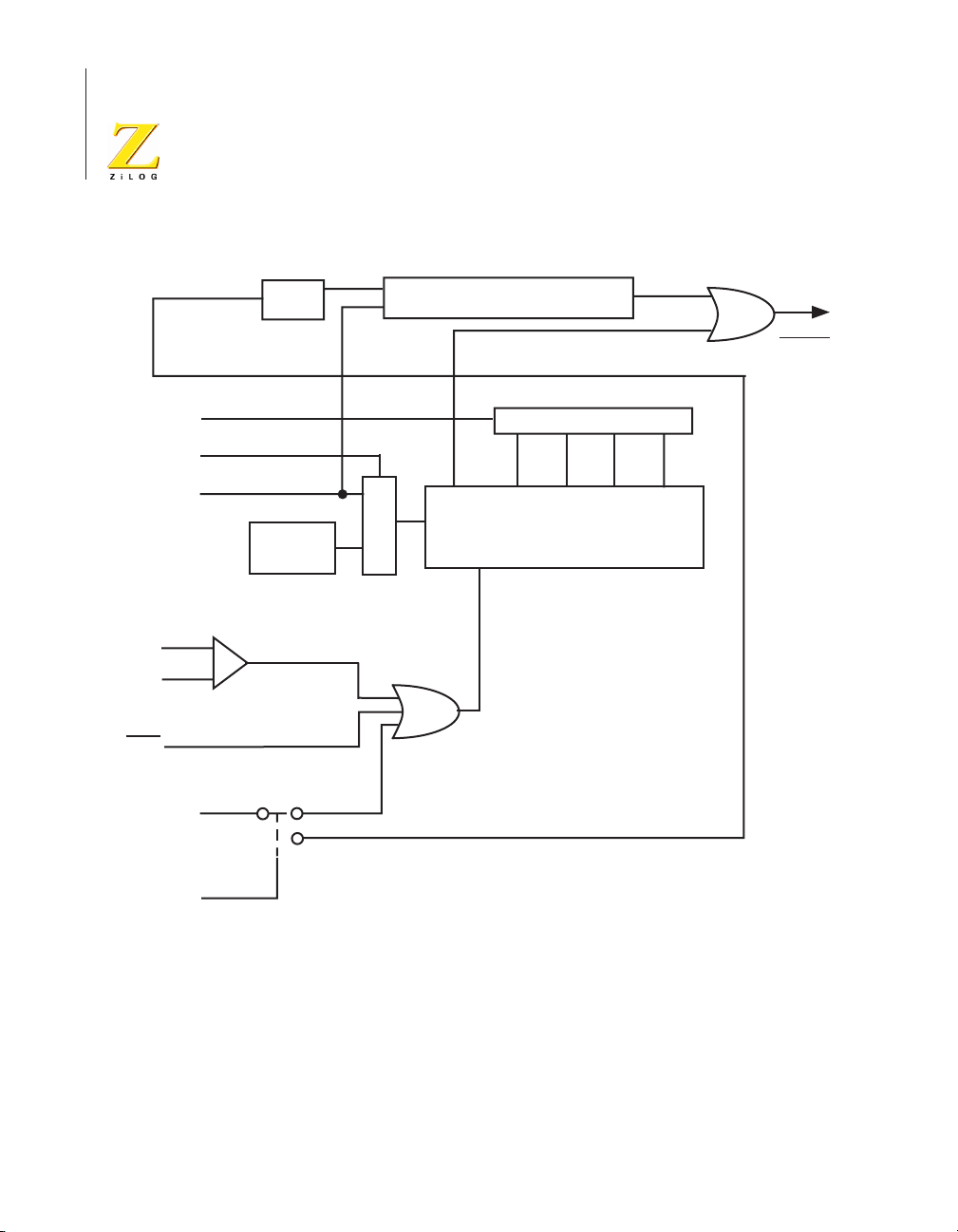
Z8 Family of Microcontrollers
User Manual
54
WDT Select
(WDTMR)
CLK Source
Select (WDTMR)
XTAL
V
DD
V
LV
WDT
.
From Stop Mode
Recovery Source
4 Clock
Filter
Internal
RC OSC.
2V Operating
Voltage Det.
+
-
CLEAR
M
U
X
CLK
18 Clock RESET
Generator
5ms POR 5ms 15ms 25ms 100ms
CLK
WDT/POR Counter Chain
CLR
RESET
WDT TAP SELECT
Internal
RESET
Stop Delay
Select (SMR)
Figure 25. Example of Z8 Reset with WDT, SMR, and POR
Reset UM001602-0904
Page 73

Watch–Dog Timer
The Watch-Dog Timer (WDT) is a retriggerable one-shot timer that resets
the Z8® CPU if it reaches its terminal count. When operating in the RUN
or HALT modes, a WDT reset is functionally equivalent to a hardware
POR reset. The WDT is initially enabled by executing the WDT instruction and refreshed on subsequent executions of the WDT instruction. The
WDT cannot be disabled after it has been initially enabled. Permanently
enabled WDTs are always enabled and the WDT instruction is used to
refresh it. The WDT circuit is driven by an on-board RC oscillator or
external oscillator from the XTAL1 pin. The POR clock source is selected
with bit 4 of the Watch–Dog Timer Mode register (WDTMR). In some
cases, a Z8 that offers the WDT but does not have a WDTMR register, has
a fixed WDT time-out and uses the on board RC oscillator as the only
clock source. Please refer to specific product specifications for selectability of time-out, WDT during HALT and STOP modes, source of WDT
clock, and availability of the permanently-on WDT option.
Z8 CPU
User Manual
55
Execution of the WDT instruction affects the Z (zero), S (sign), and V
(overflow) flags.
UM001602-0904 Watch–Dog Timer
Page 74

Z8 Family of Microcontrollers
User Manual
56
WDTMR (F) 0F
D7 D6 D5 D4 D3 D2 D1 D0
Select for WDT
* Must be 0 for Z86C03
** Default setting after RESET
INT
WDT RC SYS
TAP* OSC CLK
00 5 128
01** 10 256
10 20 512
11 80 2048
WDT During HALT
0 OFF
1 ON *
WDT During STOP
0 OFF
1 ON *
XTAL1/INT RC
0 On-Board RC *
1 XTAL
Reserved (Must be 0)
Reserved (Must be 0)
Figure 26. Example of Z8 Watch–Dog Timer Mode Register (Write-
Only)
The WDTMR register is accessible only during the first 60 processor
cycles from the execution of the first instruction after Power-On Reset,
Watch–Dog Reset or a Stop-Mode Recovery. After this point, the register
cannot be modified by any means, intentional or otherwise. The WDTMR
is a write-only register.
WDTMR is located in Expanded Register File Bank F, register 0Fh. This
register’s control bits are described on the next two pages.
Watch–Dog Timer UM001602-0904
Page 75

Z8 CPU
User Manual
WDT Time Select. Bits D1 and D0 control a tap circuit that determines
the time-out period. Table 16 shows the different values that can be
obtained. The default value of D1 and D0 are 0 and 1, respectively.
Table 16. Time-Out Period of the WDT
57
Time-Out of
0 0 5 ms min 256 TpC
0 1 15 ms min 512 TpC
1 0 25 ms min 1024 TpC
1 1 100 ms min 4096 TpC
*Notes: The values given are for VCC = 5.0V. See the device product specification
for exact WDTMR time out select options available.
1. TpC = XTAL clock cycle
2. The default on reset is, D0 = 1 and D1 = 0.
Typical Time-Out of
Internal RC OSC System ClockD1 D0
WDT During HALT. The D2 bit determines whether or not the WDT is
active during HALT mode. A 1 indicates active during HALT. The default
is 1. A WDT time out during HALT mode will reset control register ports
to their default reset conditions.
WDT During STOP. The D3 bit determines whether or not the WDT is
active during STOP mode. Because XTAL clock is stopped during STOP
mode, unless as specified below, the on-board RC must be selected as the
clock source to the POR counter. A 1 indicates active during STOP. The
default is 1. If bits D3 and D4 are both set to 1, the WDT only, is driven
by the external clock during STOP mode. This feature makes it possible
to wake up from STOP mode from an internal source. Please refer to specific product specifications for conditions of control and port registers
when the Z8® CPU comes out of STOP mode. A WDT time out during
STOP mode will not reset all control registers. The reset conditions of the
ports from STOP mode due to WDT time out is the same as if recovered
using any of the other STOP mode sources.
UM001602-0904 Watch–Dog Timer
Page 76

Z8 Family of Microcontrollers
User Manual
58
Clock Source for WDT. The D4 bit determines which oscillator source
is used to clock the internal POR and WDT counter chain. If the bit is a 1,
the internal RC oscillator is bypassed and the POR and WDT clock source
is driven from the external pin, XTAL1. The default configuration of this
bit is 0, which selects the internal RC oscillator.
Bits 5, 6, and 7. These bits are reserved.
VCC Voltage Comparator. An on-board voltage comparator checks that
VCC is at the required level to insure correct operation of the device. Reset
is globally driven if VCC is below the specified voltage. This feature is
available in select ROM Z8 devices. See the device product specification
for feature availability and operating range.
Power-On-Reset
A timer circuit clocked by a dedicated on-board RC oscillator is used for
the Power-On Reset (POR) timer function, T
VCC and the oscillator circuit to stabilize before instruction execution
begins.
The POR timer circuit is a one-shot timer triggered by one of three conditions:
•
Power fail to Power OK status (cold start)
•
Stop-Mode Recovery (if bit 5 of SMR = 1)
•
WDT time-out
The POR time is specified as T
Mode Recovery register (SMR), bit 5 selects whether the POR timer is
used after Stop-Mode Recovery or by-passed. If bit D5 = 1 then the POR
timer is used. If bit 5 = 0 then the POR timer is by-passed. In this case, the
Stop-Mode Recovery source must be held in the recovery state for 5 TPC
or 5 crystal clocks to pass the reset signal internally. This option is used
Watch–Dog Timer UM001602-0904
. On Z8 devices that feature a Stop-
POR
. This POR time allows
POR
Page 77

Z8 CPU
User Manual
when the clock is provided with an RC/LC clock. See the device product
specification for timing details.
POR (cold start) will always reset the Z8® CPU control and port registers
to their default condition. If a Z8 has a SMR register, the warm start bit
will be reset to a 0 to indicate POR.
59
VBO
WDT
POR
(Cold Start)
P27
(Stop Mode)
INT OSC
Delay Line
T
ms
POR
XTAL OSC
18 CLK
Reset Filter
Figure 27. Example of Z8 with Simple SMR and POR
Chip
Reset
UM001602-0904 Watch–Dog Timer
Page 78

Z8 Family of Microcontrollers
User Manual
60
Watch–Dog Timer UM001602-0904
Page 79

I/O Ports
The Z8® CPU features up to 32 lines dedicated to input and output. These
lines are grouped into four 8-bit ports known as Port 0, Port 1, Port 2, and
Port 3. Port 0 is nibble programmable as input, output, or address. Port 1
is byte configurable as input, output, or address/data. Port 2 is bit programmable as either inputs or outputs, with or without handshake and
SPI. Port 3 can be programmed to provide timing, serial and parallel
input/output, or comparator input/output.
All ports have push–pull CMOS outputs. In addition, the push–pull outputs of Port 2 can be turned off for open-drain operation.
Mode Registers
Z8 CPU
User Manual
61
Each port has an associated Mode Register that determines the port’s
functions and allows dynamic change in port functions during program
execution. Port and Mode Registers are mapped into the Standard Register File as shown in Figure 28.
UM001602-0904 I/O Ports
Page 80

Z8 Family of Microcontrollers
User Manual
62
Register
Port 0–1 Mode
Port 3 Mode
Port 2 Mode
Port 3
Port 2
Port 1
Port 0
HEX
F8h
F7h
F6h
03h
02h
01h
00h
Identifier
P01M
P3M
P2M
P3
P2
P1
P0
Figure 28. I/O Ports and Mode Registers
Because of their close association, Port and Mode registers are treated
like any other general-purpose register. There are no special instructions
for port manipulation. Any instruction which addresses a register can
address the ports. Data can be directly accessed in the Port Register, with
no extra moves.
Input and Output Registers
Each bit of Ports 0, 1, and 2, have an input register, an output register,
associated buffer, and control logic. Because there are separate input and
output registers associated with each port, writing to bits defined as inputs
stores the data in the output register. This data cannot be read as long as
the bits are defined as inputs. However, if the bits are reconfigured as outputs, the data stored in the output register is reflected on the output pins
I/O Ports UM001602-0904
Page 81

Z8 CPU
User Manual
and can then be read. This mechanism allows the user to initialize the outputs prior to driving their loads (see Figure 29).
Because port inputs are asynchronous to the Z8® CPU internal clock, a
READ operation could occur during an input transition. In this case, the
logic level might be uncertain (somewhere between a logic 1 and 0). To
eliminate this meta-stable condition, the Z8® CPU latches the input data
two clock periods prior to the execution of the current instruction. The
input register uses these two clock periods to stabilize to a legitimate logic
level before the instruction reads the data.
63
Note:
Port 0
The following sections describe the generic function of the Z8® CPU
ports. Any additional features of the ports such as SPI, C/T, and StopMode Recovery are covered in their own section.
This section deals with only the I/O operation of Port 0. The port's external memory interface operation is covered later in this manual. Figure 29
shows a block diagram of Port 0. This diagram also applies to Ports 1 and
2.
UM001602-0904 I/O Ports
Page 82

Z8 Family of Microcontrollers
User Manual
64
Port I/O
Lines
8 8
Input
Register
Read
Port
8
Write
Port
Output
Register
E
Handshake
Selected
Internal
Timing
88
Input
Buffer
Handshake
Handshake
Logic
Logic
Output
Buffer
8
DAV/RDY
RDY/DAV
8
Output
Enable
Internal
Bus
Figure 29. Ports 0, 1, 2 Generic Block Diagram
I/O Ports UM001602-0904
Page 83

General I/O Mode
Port 0 can be an 8-bit, bidirectional, CMOS or TTL compatible I/O port.
These eight I/O lines can be configured under software control as a nibble
I/O port (P03–P00 input/output and P07–P04 input/output), or as an
address port for interfacing external memory. The input buffers can be
Schmitt-triggered, level shifted, or a single-trip point buffer and can be
nibble programmed. Either nibble output can be globally programmed as
push–pull or open-drain. Low EMI output buffers in some cases can be
globally programmed by the software as an OTP program option or as a
ROM mask option. In such cases, the Z8® MCU features autolatches that
are hardwired to the inputs. Please refer to the specific Z8 MCU product
specification for the exact input/output buffer features that are available
(see Figures 30 and 31).
Z8 CPU
User Manual
65
UM001602-0904 I/O Ports
Page 84

Z8 Family of Microcontrollers
User Manual
66
OPEN-DRAIN
OEN
OUT
IN
1.5
Z8
4
4
2.3V Hysteresis
Port 1
(I/O or AD15–AD08)
Handshake Controls
DAV0 and RDY0
(P32 and P35)
PIN
Autolatch
R ≈ 500 KΩ
Figure 30. Port 0 Configuration with Open-Drain Capability,
Autolatch, and Schmitt-Trigger
I/O Ports UM001602-0904
Page 85
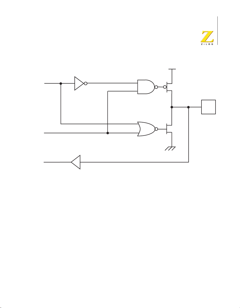
OEN
OUT
Z8 CPU
User Manual
67
PIN
TTL Level Shifter
IN
Figure 31. Port 0 Configuration with TTL Level Shifter
Read/Write Operations
In the nibble I/0 Mode, Port 0 is accessed as general-purpose register P0
(00h) with ERF Bank set to 0. The port is written by specifying P0 as an
instruction's destination register. Writing to the port causes data to be
stored in the port's output register.
The port is read by specifying P0 as the source register of an instruction.
When an output nibble is read, data on the external pins is returned.
Under normal loading conditions this is equivalent to reading the output
register. However, for Port 0 outputs defined as open–drain, the data
returned is the value forced on the output by the external system. This
may not be the same as the data in the output register. Reading a nibble
defined as input also returns data on the external pins. However, input bits
UM001602-0904 I/O Ports
Page 86

Z8 Family of Microcontrollers
User Manual
68
under handshake control return data latched into the input register via the
input strobe.
The Port 0–1 Mode resistor bits D1–D0 and D7–D6 are used to configure
Port 0 nibbles. The lower nibble (P00–P03) can be defined as inputs by
setting bits D1 to 0 and D0 to 1, or as outputs by setting both D1 and D0
to 0. Likewise, the upper nibble (P04–P07) can be defined as inputs by
setting bits D7 to 0 and D6 to 1, or as outputs by setting both D6 and D7
to 0 (see Figure 32).
Handshake Operation
When used as an I/0 port, Port 0 can be placed under handshake control
by programming the Port 3 Mode register bit D2 to 1. In this configuration, handshake control lines are DAV0 (P32) and RDY0 (P35) when Port
0 is an input port, or RDY0 (P32) and DAV0 (P35) when Port 0 is an output port (see Figure 33).
Handshake direction is determined by the configuration (input or output)
assigned to the Port 0 upper nibble, P04–P07. The lower nibble must have
the same I/0 configuration as the upper nibble to be under handshake control. Figure 30 illustrates the Port 0 upper and lower nibbles and the associated handshake lines of Port 3.
Port 1
This section deals only with the I/0 operation. The port's external memory
interface operation is discussed later in this manual. Figure 29 shows a
block diagram of Port 1.
General I/O Mode
Port 1 can be an 8-bit, bidirectional, CMOS or TTL compatible port with
multiplexed address (A7–A0) and data (D7–D0) ports. These eight I/O
lines can be byte programmed as inputs or outputs or can be configured
under software control as an Address/Data port for interfacing to external
I/O Ports UM001602-0904
Page 87

Z8 CPU
User Manual
memory. The input buffers can be Schmitt-triggered, level- shifted, or a
single-point buffer. In some cases, the output buffers can be globally programmed as either push–pull or open-drain. Low-EMI output buffers can
be globally programmed by software, as an OTP program option, or as a
ROM Mask Option. In some cases, the Z8® MCU can have autolatches
hardwired to the inputs. Please refer to specific product specifications for
exact input/output buffer-type features available (Figures 32 and 33).
Register F8h (P01M)
Port 0–1 Mode Register (P01M)
(Write-Only)
D7 D6 D1 D0
69
P04–P07 Mode
00 = Output
01 = Input
1X = A12–A15
P00–P03 Mode
00 = Output
01 = Input
1X = A8–A11
Figure 32. Port 0 I/O Operation
Register F7h
Port 3 Mode Register (P3M)
(Write-Only)
D2
0 P32 = Input
P35 = Output
1 P32 = DAV0/RDY0
P35 = RDY0/DAV0
Figure 33. Port 0 Handshake Operation
UM001602-0904 I/O Ports
Page 88

Z8 Family of Microcontrollers
User Manual
70
OPEN-DRAIN
OEN
OUT
IN
1.5
Z8
8
2.3V Hysteresis
Port 1
(I/O or AD7–AD0)
Handshake Controls
DAV1 and RDY1
(P33 and P34)
PIN
Autolatch
R ≈ 500 KΩ
Figure 34. Port 1 Configuration with Open-Drain Capability,
Autolatch, and Schmitt-Trigger
I/O Ports UM001602-0904
Page 89

Z8 CPU
User Manual
71
OEN
OUT
IN
Z8
TTL Level Shifter
8
Port 1
(I/O or AD7–AD0)
Handshake Controls
DAV1 and RDY1
(P33 and P34)
PIN
Figure 35. Port 1 Configuration with TTL Level Shifter
Read/Write Operations
In byte input or byte output mode, the port is accessed as General-Purpose
Register P1 (01h). The port is written by specifying P1 as an instruction's
UM001602-0904 I/O Ports
Page 90

Z8 Family of Microcontrollers
User Manual
72
destination register. Writing to the port causes data to be stored in the
port's output register.
The port is read by specifying P1 as the source register of an instruction.
When an output is read, data on the external pins is returned. Under normal loading conditions, this is equivalent to reading the output register.
However, if Port 1 outputs are defined as open-drain, the data returned is
the value forced on the output by the external system. This may not be the
same as the data in the output register. When Port 1 is defined as an input,
reading also returns data on the external pins. However, inputs under
handshake control return data latched into the input register via the input
strobe.
Using the Port 0–1 Mode Register, Port 1 is configured as an output port
by setting bits D4 and D3 to 0, or as an input port by setting D4 to 0 and
D3 to 1 (see Figure 36).
R248 P01M
Port 0–1 Mode Register
(F8, Write-Only)
D4 D3
P10–P13 Mode
00 = Byte Output
01 = Byte Output
10 = AD0-AD7
11 = High Impedance AD0–AD7,
AS, DS, R/W,
A8–A11, A12–A15
Figure 36. Port 1 I/O Operation
I/O Ports UM001602-0904
Page 91

Handshake Operations
When used as an I/O port, Port 1 can be placed under handshake control
by programming the Port 3 Mode register bits D4 and D3 both to 1. In this
configuration, handshake control lines are DAV1 (P33) and RDY1 (P34)
when Port 1 is an input port, or RDY1 (P33) and DAV1 (P34) when Port 1
is an output port. See Figures 37 and 39.
Handshake direction is determined by the configuration (input and output)
assigned to Port 1. For example, if Port 1 is an output port then handshake
is defined as output.
R247 P3M
Port 3 Mode Register
(F7, Write-Only)
D4 D3
Z8 CPU
User Manual
73
00 P33 = Input P34 = Output
01 P33 = Input P34 = DM
10 P33 = Input P34 = DM
11 P33 = DAV1/RDY1 P34 = RDY1/DAV1
Figure 37. Handshake Operation
Port 2
Port 2 is a general-purpose port. Figure 29 shows a block diagram of Port
2. Each of its lines can be independently programmed as input or output
via the Port 2 Mode Register (F6h) as seen in Figure 38. A bit set to a 1 in
P2M configures the corresponding bit in Port 2 as an input, while a bit set
to 0 configures an output line.
UM001602-0904 I/O Ports
Page 92

Z8 Family of Microcontrollers
User Manual
74
Register F6h
Port 2 Mode Register (P2M)
(Write-Only)
D7 D6 D5 D4 D3 D2 D1 D0
Figure 38. Port 2 I/O Mode Configuration
General Port I/O
Port 2 can be an 8-bit, bidirectional, CMOS- or TTL- compatible I/O port.
These eight I/O lines can be configured under software control to be an
input or output, independently. Input buffers can be Schmitt-triggered,
level-shifted, or a single trip point buffer and may contain autolatches.
Bits programmed as outputs may be globally programmed as either push–
pull or open-drain. Low-EMI output buffers can be globally programmed
by the software, an OTP program option, or as a ROM mask option. In
addition, when the SPI is featured and enabled, P20 functions as data-in
(DI), and P27 functions as data-out (DO). Please refer to specific product
specifications for exact input/output buffer type features available. See
Figures 39 through 41.
Port 2 Mode
0 = Output
1 = Input
I/O Ports UM001602-0904
Page 93

OPEN-DRAIN
P21–P26 OE
P21–P26 OUT
Z8 CPU
User Manual
75
P21–P26
PIN
P21–P26 IN
1.5
2.3V Hysteresis @ VCC = 5.0V
Autolatch
R ≈ 500 KΩ
Figure 39. Port 2 Configuration with Open-Drain Capability,
Autolatch, and Schmitt-Trigger
UM001602-0904 I/O Ports
Page 94

Z8 Family of Microcontrollers
User Manual
76
Open-Drain
OEN
OUT
TTL Level Shifter
IN
PIN
Figure 40. Port 2 Configuration with TTL Level Shifter
I/O Ports UM001602-0904
Page 95

OPEN-DRAIN
P20 OE
SPI EN
P20 OUT
P20 IN
or
SPI DI
OPEN-DRAIN
Z8 CPU
User Manual
77
P20
PIN
Autolatch
R ≈ 500 KΩ
P27 OUT
SPI DO
SPI DO
P27 OE
SPI Active
P27 IN
Standard
SPI
Standard
SPI
SCON
D2
0 SOI D0 Enable
1 P27 OUT
*SPI must be enabled with D0
R ≈ 500 KΩ
P27
PIN
Autolatch
Figure 41. Port 2 Configuration with Open-Drain Capability,
Autolatch, Schmitt-Trigger and SPI
UM001602-0904 I/O Ports
Page 96

Z8 Family of Microcontrollers
User Manual
78
Read/Write Operations
Port 2 is accessed as General-Purpose Register P2 (02h). Port 2 is written
by specifying P2 as an instruction’s destination register. Writing to Port 2
causes data to be stored in the output register of Port 2, and reflected
externally on any bit configured as an output.
Port 2 is read by specifying P2 as the source register of an instruction.
When an output bit is read, data on the external
pin is returned. Under normal loading conditions, this is equivalent to
reading the output register. However, if a bit of Port 2 is defined as an
open-drain output, the data returned is the value forced on the output pin
by the external system. This may not be the same as the data in the output
register. Reading input bits of Port 2 also returns data on the external pins.
However, inputs under handshake control return data latched into the
input register via the input strobe.
Handshake Operation
Port 2 can be placed under handshake control by programming bit 6 in the
Port 3 Mode Register (see Figure 42). In this configuration, Port 3 lines
P31 and P36 are used as the handshake control lines DAV2 and RDY2 for
input handshake, or RDY2 and DAV2 for output handshake.
Handshake direction is determined by the configuration (input or output)
assigned to bit 7 of Port 2. Only those bits with the same configuration as
P27 will be under handshake control. Figure 43 illustrates the bit lines of
Port 2 and the associated handshake lines of Port 3.
I/O Ports UM001602-0904
Page 97

Register F7h
Port 3 Mode Register
(Write-Only)
D7 D6 D5 D4 D3 D2 D1 D0
Port 2 Handshaking
0 P31 = Input (TIN) P36 = Output (T
1 P31 = DAV2/RDY2 P36 = RDY2/DAV2
Figure 42. Port 2 Handshake Configuration
P20
OUT
)
Z8 CPU
User Manual
79
Port 2 (I/O)
P27
Handshake Controls
DAV2 and RDY2
(P31 and P36)
Figure 43. Port 2 Handshaking
UM001602-0904 I/O Ports
Page 98

Z8 Family of Microcontrollers
User Manual
80
Port 3
General Port I/O
Port 3 differs structurally from Port 0, 1, and 2. Port 3 lines are fixed as
four inputs (P33–P30) and four outputs (P37–P34) Port 3 does not have
an input and output register for each bit. Instead, all of the input lines have
one input register, and all of the output lines have an output register. Port
3 can be a CMOS- or TTL- compatible I/O port. Under software control,
the lines can be configured as special control lines for handshake, comparator inputs, SPI control, external memory status, or I/O lines for the
on-board serial and timer facilities. Figure 44 is a generic block diagram
of Port 3.
The inputs can be Schmitt-triggered, level-shifted, or single-trip point
buffered. In some cases, the Z8® MCU may have autolatches hardwired
on certain Port 3 inputs and Low-EMI capabilities on the outputs. Please
refer to specific product specifications for exact input/output buffer type
features. Please refer to the section on counter/timers, Stop-Mode Recovery, serial I/O, comparators, and interrupts for more information on the
relationships of Port 3 to that feature.
I/O Ports UM001602-0904
Page 99

Z8 CPU
User Manual
81
Read
Port
Input
4
Read
4
Port
4
Input
Register
Output
Data
Return
Buffer
4
To Interrupt Timer,
Handshake Logic,
or Serial I/O
Input
Buffer
Buffer
Port
Input
4
Lines
P30–P3
3
Write
Port
4
Internal
Bus
Output
Output
Output
Register
Register
Register
4
From Timer,
Handshake Logic,
or Serial I/O
Output
Output
Buffer
Buffer
Port
Output
4
Lines
P34–P3
7
Figure 44. Port 3 Block Diagram
UM001602-0904 I/O Ports
Page 100

Z8 Family of Microcontrollers
User Manual
82
I/O Ports UM001602-0904
 Loading...