

Page 1

Z8051™ Family of 8-Bit Microcontrollers
Z8051 On-Chip Debugger
and In-System Programmer
User Manual
UM024002-0512
Copyright ©2012 Zilog®, Inc. All rights reserved.
www.zilog.com
Page 2

Z8051 On-Chip Debugger and In-System Programmer
Warning:
User Manual
DO NOT USE THIS PRODUCT IN LIFE SUPPORT SYSTEMS.
LIFE SUPPORT POLICY
ZILOG’S PRODUCTS ARE NOT AUTHORIZED FOR USE AS CRITICAL COMPONENTS IN LIFE
SUPPORT DEVICES OR SYSTEMS WITHOUT THE EXPRESS PRIOR WRITTEN APPROVAL OF
THE PRESIDENT AND GENERAL COUNSEL OF ZILOG CORPORATION.
As used herein
Life support devices or systems are devices which (a) are intended for surgical implant into the body, or (b)
support or sustain life and whose failure to perform when properly used in accordance with instructions for
use provided in the labeling can be reasonably expected to result in a significant injury to the user. A critical component is any componen t in a li fe supp ort device o r syste m whose failure to p erform ca n be re asonably expected to cause the failure of the life support device or system or to affect its safety or effectiveness.
ii
Document Disclaimer
©2012 Zilog, Inc. All rights reserved. Information in this publication concerning the devices, applications,
or technology described is intended to suggest possible uses and may be superseded. ZILOG, INC. DOES
NOT ASSUME LIABILITY FOR OR PROVIDE A REPRESENTATION OF ACCURACY OF THE
INFORMATION, DEVICES, OR TECHNOLOGY DESCRIBED IN THIS DOC UMENT. ZILOG ALSO
DOES NOT ASSUME LIABILITY FOR INTELLECTUAL PROPERTY INFRINGEMENT RELATED
IN ANY MANNER TO USE OF INFORMATION, DEVICES, OR TECHNOLOGY DESCRIBED
HEREIN OR OTHERWISE. The information contained within this document has been verified according
to the general principles of electrical and mechanical engineering.
Z8051 is a trademark or registered trademark of Zilog, Inc. All other product or service names are the
property of their respective owners.
UM024002-0512
Page 3

Revision History
Each instance in the Revision History table below reflects a change to this document from
its previous version.
Z8051 On-Chip Debugger and In-System Programmer
User Manual
iii
Date
May
2012
Mar
2012
Revision
Level Description
02 Updated for improved usability. All
01 Original issue. All
Page
No
UM024002-0512 Revision History
Page 4

Table of Contents
Revision History . . . . . . . . . . . . . . . . . . . . . . . . . . . . . . . . . . . . . . . . . . . . . . . . . . . . . . . . . . . . .iii
List of Figures . . . . . . . . . . . . . . . . . . . . . . . . . . . . . . . . . . . . . . . . . . . . . . . . . . . . . . . . . . . . . . .vi
Introduction. . . . . . . . . . . . . . . . . . . . . . . . . . . . . . . . . . . . . . . . . . . . . . . . . . . . . . . . . . . . . . . . . 1
The Z8051 On-Chip Debugger . . . . . . . . . . . . . . . . . . . . . . . . . . . . . . . . . . . . . . . . . . . . . . . . . . 2
Features . . . . . . . . . . . . . . . . . . . . . . . . . . . . . . . . . . . . . . . . . . . . . . . . . . . . . . . . . . . . 3
Install the Z8051 OCD Software and Documentation . . . . . . . . . . . . . . . . . . . . . . . . . . . 3
Z8051 OCD Driver Installation . . . . . . . . . . . . . . . . . . . . . . . . . . . . . . . . . . . . . . . . . 4
Understanding the OCD Menu Functions . . . . . . . . . . . . . . . . . . . . . . . . . . . . . . . . . . . . 12
File Menu . . . . . . . . . . . . . . . . . . . . . . . . . . . . . . . . . . . . . . . . . . . . . . . . . . . . . . . . . 12
Emulation Menu . . . . . . . . . . . . . . . . . . . . . . . . . . . . . . . . . . . . . . . . . . . . . . . . . . . . 15
Break/Configure Menu . . . . . . . . . . . . . . . . . . . . . . . . . . . . . . . . . . . . . . . . . . . . . . . 17
View Menu . . . . . . . . . . . . . . . . . . . . . . . . . . . . . . . . . . . . . . . . . . . . . . . . . . . . . . . . 21
Window Menu . . . . . . . . . . . . . . . . . . . . . . . . . . . . . . . . . . . . . . . . . . . . . . . . . . . . . 31
Z8051 On-Chip Debugger and In-System Programmer
User Manual
iv
Child Windows . . . . . . . . . . . . . . . . . . . . . . . . . . . . . . . . . . . . . . . . . . . . . . . . . . . . . . . . 34
Z8051 Basic Registers Window . . . . . . . . . . . . . . . . . . . . . . . . . . . . . . . . . . . . . . . . 34
Code Disassemble Window . . . . . . . . . . . . . . . . . . . . . . . . . . . . . . . . . . . . . . . . . . . 37
Code Dump Window . . . . . . . . . . . . . . . . . . . . . . . . . . . . . . . . . . . . . . . . . . . . . . . . 40
XDATA Dump Window . . . . . . . . . . . . . . . . . . . . . . . . . . . . . . . . . . . . . . . . . . . . . . 44
IRAM Dump Window . . . . . . . . . . . . . . . . . . . . . . . . . . . . . . . . . . . . . . . . . . . . . . . 48
SFR Dump Window . . . . . . . . . . . . . . . . . . . . . . . . . . . . . . . . . . . . . . . . . . . . . . . . . 50
Watch Global Window . . . . . . . . . . . . . . . . . . . . . . . . . . . . . . . . . . . . . . . . . . . . . . . 52
Watch Local Window . . . . . . . . . . . . . . . . . . . . . . . . . . . . . . . . . . . . . . . . . . . . . . . . 54
Text File Window . . . . . . . . . . . . . . . . . . . . . . . . . . . . . . . . . . . . . . . . . . . . . . . . . . . 57
The Z8051 OCD In-System Programmer. . . . . . . . . . . . . . . . . . . . . . . . . . . . . . . . . . . . . . . . . 64
Features . . . . . . . . . . . . . . . . . . . . . . . . . . . . . . . . . . . . . . . . . . . . . . . . . . . . . . . . . . . 65
Connect the Hardware . . . . . . . . . . . . . . . . . . . . . . . . . . . . . . . . . . . . . . . . . . . . . . . . . . . 65
Apply Power . . . . . . . . . . . . . . . . . . . . . . . . . . . . . . . . . . . . . . . . . . . . . . . . . . . . . . . . . . 66
Understanding the OCD ISP Menu Functions . . . . . . . . . . . . . . . . . . . . . . . . . . . . . . . . 66
HexData Menu . . . . . . . . . . . . . . . . . . . . . . . . . . . . . . . . . . . . . . . . . . . . . . . . . . . . . 66
Program Menu . . . . . . . . . . . . . . . . . . . . . . . . . . . . . . . . . . . . . . . . . . . . . . . . . . . . . 73
Window Menu . . . . . . . . . . . . . . . . . . . . . . . . . . . . . . . . . . . . . . . . . . . . . . . . . . . . . 75
UM024002-0512 Table of Contents
Page 5

Z8051 On-Chip Debugger and In-System Programmer
User Manual
Child Windows . . . . . . . . . . . . . . . . . . . . . . . . . . . . . . . . . . . . . . . . . . . . . . . . . . . . . . . . 79
Code Dump Window . . . . . . . . . . . . . . . . . . . . . . . . . . . . . . . . . . . . . . . . . . . . . . . . 80
XData Dump Window . . . . . . . . . . . . . . . . . . . . . . . . . . . . . . . . . . . . . . . . . . . . . . . 81
Appendix A. OCD Driver Installation on Windows Vista Systems . . . . . . . . . . . . . . . . 82
Appendix B. OCD Driver Installation on Windows XP Systems . . . . . . . . . . . . . . . . . . 85
Customer Support . . . . . . . . . . . . . . . . . . . . . . . . . . . . . . . . . . . . . . . . . . . . . . . . . . . . . . . . . . . 88
v
UM024002-0512 Table of Contents
Page 6

List of Figures
Figure 1. On-Chip Debugger Screen . . . . . . . . . . . . . . . . . . . . . . . . . . . . . . . . . . . . . . . 2
Figure 2. Install Device Driver Dialog, Windows 7 . . . . . . . . . . . . . . . . . . . . . . . . . . . 5
Figure 3. Browse For Driver Dialog, Windows Vista . . . . . . . . . . . . . . . . . . . . . . . . . . 6
Figure 4. Can’t Verify Publisher Dialog, Windows Vista . . . . . . . . . . . . . . . . . . . . . . 7
Figure 5. Successfully Installed Dialog, Windows Vista . . . . . . . . . . . . . . . . . . . . . . . 8
Figure 6. Unsuccessful Installation, Scenario 1 . . . . . . . . . . . . . . . . . . . . . . . . . . . . . . 9
Figure 7. Unsuccessful Installation, Scenario 2 . . . . . . . . . . . . . . . . . . . . . . . . . . . . . 10
Figure 8. Device Manager Dialog, Windows 7 . . . . . . . . . . . . . . . . . . . . . . . . . . . . . . 11
Figure 9. The OCD’s File Menu . . . . . . . . . . . . . . . . . . . . . . . . . . . . . . . . . . . . . . . . . 12
Figure 10. Object File Dialog . . . . . . . . . . . . . . . . . . . . . . . . . . . . . . . . . . . . . . . . . . . . 13
Figure 11. Open File Dialog . . . . . . . . . . . . . . . . . . . . . . . . . . . . . . . . . . . . . . . . . . . . . 14
Figure 12. Break Debug Dialog . . . . . . . . . . . . . . . . . . . . . . . . . . . . . . . . . . . . . . . . . . 14
Figure 13. The OCD’s Emulation Menu . . . . . . . . . . . . . . . . . . . . . . . . . . . . . . . . . . . . 15
Figure 14. The OCD’s Break/Configure Menu . . . . . . . . . . . . . . . . . . . . . . . . . . . . . . . 17
Figure 15. Break Control Dialog . . . . . . . . . . . . . . . . . . . . . . . . . . . . . . . . . . . . . . . . . . 18
Figure 16. Break BEFORE Timing Diagram . . . . . . . . . . . . . . . . . . . . . . . . . . . . . . . . 18
Figure 17. Break AFTER Timing Diagram . . . . . . . . . . . . . . . . . . . . . . . . . . . . . . . . . 19
Figure 18. Peripheral Control Dialog . . . . . . . . . . . . . . . . . . . . . . . . . . . . . . . . . . . . . . 19
Figure 19. Z51F0811 MCU Configuration Example . . . . . . . . . . . . . . . . . . . . . . . . . . 20
Figure 20. The OCD’s View Menu . . . . . . . . . . . . . . . . . . . . . . . . . . . . . . . . . . . . . . . . 22
Figure 21. The Basic Registers Dialog . . . . . . . . . . . . . . . . . . . . . . . . . . . . . . . . . . . . . 23
Figure 22. Code Disassembler Dialog . . . . . . . . . . . . . . . . . . . . . . . . . . . . . . . . . . . . . . 24
Figure 23. Code Dump Dialog . . . . . . . . . . . . . . . . . . . . . . . . . . . . . . . . . . . . . . . . . . . 25
Figure 24. XDATA Dump Dialog . . . . . . . . . . . . . . . . . . . . . . . . . . . . . . . . . . . . . . . . . 26
Figure 25. IRAM Dump Dialog . . . . . . . . . . . . . . . . . . . . . . . . . . . . . . . . . . . . . . . . . . 27
Figure 26. SFR Dump Dialog . . . . . . . . . . . . . . . . . . . . . . . . . . . . . . . . . . . . . . . . . . . . 28
Figure 27. Global Variables Dialog . . . . . . . . . . . . . . . . . . . . . . . . . . . . . . . . . . . . . . . 28
Figure 28. Local Function Dialog . . . . . . . . . . . . . . . . . . . . . . . . . . . . . . . . . . . . . . . . . 29
Figure 29. A Sample Text File . . . . . . . . . . . . . . . . . . . . . . . . . . . . . . . . . . . . . . . . . . . 30
Figure 30. The OCD’s Window Menu . . . . . . . . . . . . . . . . . . . . . . . . . . . . . . . . . . . . . 31
Figure 31. Cascaded Windows . . . . . . . . . . . . . . . . . . . . . . . . . . . . . . . . . . . . . . . . . . . 32
Figure 32. Tiled Windows . . . . . . . . . . . . . . . . . . . . . . . . . . . . . . . . . . . . . . . . . . . . . . . 33
Figure 33. Using the Basic Registers Function, #1 of 6 . . . . . . . . . . . . . . . . . . . . . . . . 34
Z8051 On-Chip Debugger and In-System Programmer
User Manual
vi
UM024002-0512 List of Figures
Page 7

Z8051 On-Chip Debugger and In-System Programmer
User Manual
Figure 34. Using the Basic Registers Function, #2 of 6 . . . . . . . . . . . . . . . . . . . . . . . . 35
Figure 35. Using the Basic Registers Function, #3 of 6 . . . . . . . . . . . . . . . . . . . . . . . . 35
Figure 36. Using the Basic Registers Function, #4 of 6 . . . . . . . . . . . . . . . . . . . . . . . . 36
Figure 37. Using the Basic Registers Function, #5 of 6 . . . . . . . . . . . . . . . . . . . . . . . . 36
Figure 38. Using the Basic Registers Function, #6 of 6 . . . . . . . . . . . . . . . . . . . . . . . . 37
Figure 39. Using the Code Disassembler Function, #1 of 3 . . . . . . . . . . . . . . . . . . . . . 38
Figure 40. Using the Code Disassembler Function, #2 of 3 . . . . . . . . . . . . . . . . . . . . . 38
Figure 41. Using the Code Assembler Function, #3 of 3 . . . . . . . . . . . . . . . . . . . . . . . 39
Figure 42. Using the PC Break Toggle Function . . . . . . . . . . . . . . . . . . . . . . . . . . . . . 40
Figure 43. Using the Code Dump Function, #1 of 2 . . . . . . . . . . . . . . . . . . . . . . . . . . . 41
Figure 44. Using the Code Dump Function, #2 of 2 . . . . . . . . . . . . . . . . . . . . . . . . . . . 42
Figure 45. The Code Dump Function’s Goto/Input Dialog . . . . . . . . . . . . . . . . . . . . . 43
Figure 46. The Code Dump Function’s Pattern Load Dialog . . . . . . . . . . . . . . . . . . . . 43
Figure 47. The Code Dump Function’s Pattern Save Dialog . . . . . . . . . . . . . . . . . . . . 44
Figure 48. The Code Dump Function’s Pattern Fill Dialog . . . . . . . . . . . . . . . . . . . . . 44
Figure 49. Using the XDATA Dump Function, #1 of 2 . . . . . . . . . . . . . . . . . . . . . . . . 45
Figure 50. Using the XDATA Dump Function, #2 of 2 . . . . . . . . . . . . . . . . . . . . . . . . 46
Figure 51. The XDATA Dump Function’s Goto/Input Dialog . . . . . . . . . . . . . . . . . . . 46
Figure 52. The XDATA Dump Function’s Pattern Load Dialog . . . . . . . . . . . . . . . . . 47
Figure 53. The XDATA Dump Function’s Pattern Save Dialog . . . . . . . . . . . . . . . . . 47
Figure 54. The XDATA Dump Function’s Pattern Fill Dialog . . . . . . . . . . . . . . . . . . 48
Figure 55. Using the IRAM Dump Function, #1 of 2 . . . . . . . . . . . . . . . . . . . . . . . . . . 49
Figure 56. Using the IRAM Dump Function, #2 of 2 . . . . . . . . . . . . . . . . . . . . . . . . . . 50
Figure 57. Using the SFR Dump Function, #1 of 3 . . . . . . . . . . . . . . . . . . . . . . . . . . . 51
Figure 58. Using the SFR Dump Function, #2 of 3 . . . . . . . . . . . . . . . . . . . . . . . . . . . 51
Figure 59. Using the SFRDump Function, #3 of 3 . . . . . . . . . . . . . . . . . . . . . . . . . . . . 52
Figure 60. The Watch Global Function’s Global Variables Dialog . . . . . . . . . . . . . . . 53
Figure 61. Adding A Global Symbol . . . . . . . . . . . . . . . . . . . . . . . . . . . . . . . . . . . . . . 53
Figure 62. Editing A Global Symbol . . . . . . . . . . . . . . . . . . . . . . . . . . . . . . . . . . . . . . 54
Figure 63. The Watch Local Function Dialog . . . . . . . . . . . . . . . . . . . . . . . . . . . . . . . . 55
Figure 64. Editing A Local Symbol . . . . . . . . . . . . . . . . . . . . . . . . . . . . . . . . . . . . . . . 55
Figure 65. Example Watch Local Function, #1 of 2 . . . . . . . . . . . . . . . . . . . . . . . . . . . 56
Figure 66. Example Watch Local Function, #2 of 2 . . . . . . . . . . . . . . . . . . . . . . . . . . . 57
Figure 67. Using the Text File Function, #1 of 5 . . . . . . . . . . . . . . . . . . . . . . . . . . . . . 58
Figure 68. Using the Text File Function, #2 of 5 . . . . . . . . . . . . . . . . . . . . . . . . . . . . . 58
Figure 69. Using the Text File Function, #3 of 5 . . . . . . . . . . . . . . . . . . . . . . . . . . . . . 59
vii
UM024002-0512 List of Figures
Page 8

Z8051 On-Chip Debugger and In-System Programmer
User Manual
Figure 70. Text File Child Window . . . . . . . . . . . . . . . . . . . . . . . . . . . . . . . . . . . . . . . 60
Figure 71. Code Disassembler Child Window . . . . . . . . . . . . . . . . . . . . . . . . . . . . . . . 61
Figure 72. Using the Text File Function, #4 of 5 . . . . . . . . . . . . . . . . . . . . . . . . . . . . . 62
Figure 73. Using the Text File Function, #5 of 5 . . . . . . . . . . . . . . . . . . . . . . . . . . . . . 63
Figure 74. Example On-Chip Debugger ISP Screen . . . . . . . . . . . . . . . . . . . . . . . . . . . 64
Figure 75. OCD Hardware ISP Pin Assignment (Bottom View) . . . . . . . . . . . . . . . . . 65
Figure 76. The OCD ISP’s File Menu . . . . . . . . . . . . . . . . . . . . . . . . . . . . . . . . . . . . . . 67
Figure 77. Device Select Dialog . . . . . . . . . . . . . . . . . . . . . . . . . . . . . . . . . . . . . . . . . . 68
Figure 78. Fill Buffer Dialog . . . . . . . . . . . . . . . . . . . . . . . . . . . . . . . . . . . . . . . . . . . . . 69
Figure 79. File Open Dialog . . . . . . . . . . . . . . . . . . . . . . . . . . . . . . . . . . . . . . . . . . . . . 70
Figure 80. OCD ISP Dialog . . . . . . . . . . . . . . . . . . . . . . . . . . . . . . . . . . . . . . . . . . . . . 71
Figure 81. Select Device To Read Dialog . . . . . . . . . . . . . . . . . . . . . . . . . . . . . . . . . . . 72
Figure 82. Most Recently Used Files . . . . . . . . . . . . . . . . . . . . . . . . . . . . . . . . . . . . . . 73
Figure 83. The OCD ISP’s Program Menu . . . . . . . . . . . . . . . . . . . . . . . . . . . . . . . . . . 73
Figure 84. Configuration Dialog . . . . . . . . . . . . . . . . . . . . . . . . . . . . . . . . . . . . . . . . . . 75
Figure 85. The OCD ISP’s Window Menu . . . . . . . . . . . . . . . . . . . . . . . . . . . . . . . . . . 76
Figure 86. Open CODE Dump Child Window . . . . . . . . . . . . . . . . . . . . . . . . . . . . . . . 76
Figure 87. Open XData Dump Child Window . . . . . . . . . . . . . . . . . . . . . . . . . . . . . . . 77
Figure 88. Cascading Child Windows . . . . . . . . . . . . . . . . . . . . . . . . . . . . . . . . . . . . . . 78
Figure 89. Tiled Child Windows . . . . . . . . . . . . . . . . . . . . . . . . . . . . . . . . . . . . . . . . . . 79
Figure 90. CODE Dump Child Window . . . . . . . . . . . . . . . . . . . . . . . . . . . . . . . . . . . . 80
Figure 91. XData Dump Child Window . . . . . . . . . . . . . . . . . . . . . . . . . . . . . . . . . . . . 81
Figure 92. Found New Hardware Dialog, Windows Vista . . . . . . . . . . . . . . . . . . . . . . 82
Figure 93. Install Device Driver Dialog, Windows Vista . . . . . . . . . . . . . . . . . . . . . . . 83
Figure 94. Couldn’t Find Driver Dialog, Windows Vista . . . . . . . . . . . . . . . . . . . . . . . 84
Figure 95. The Found New Hardware Wizard Welcome Screen . . . . . . . . . . . . . . . . . 85
Figure 96. The Found New Hardware Wizard’s Browse Screen . . . . . . . . . . . . . . . . . 86
viii
UM024002-0512 List of Figures
Page 9

Introduction
The Z8051 On-Chip Debugger (OCD) and In-System Programmer (ISP) applications have
been developed to support Zilog’ s Z8051 8-bit MCUs. This document describes how to set
up and use the Z8051 OCD and ISP programs with your Z8051 Development Kit.
Z8051 On-Chip Debugger and In-System Programmer
User Manual
1
UM024002-0512 Introduction
Page 10

Z8051 On-Chip Debugger and In-System Programmer
The Z8051 On-Chip Debugger
The Z8051 On-Chip Debugger enables a development PC to communicate with your target
Z8051-based MCU. The OCD interface is used to connect the development PC and the Z8051
MCU. The OCD controls the Z8051 MCU’s internal debugging logic, including emulation, step
run, monitoring, etc., and can read or change the value of the Z8051 MCU’s internal memory
and I/O peripherals.
The Z8051 OCD supports emulation and debugging at the maximum frequency of the MCU
and can support In-System Programming (ISP), thereby eliminating the requirement for an
expensive emulator system.
The Z8051 OCD Debugger works with the Microsoft Windows XP, Vista (32/64) and
Windows 7 (32/64) operating systems.
User Manual
2
See the example On-Chip Debugger Screen shown in Figure 1.
Figure 1. On-Chip Debugger Screen
UM024002-0512 The Z8051 On-Chip Debugger
Page 11

Z8051 On-Chip Debugger and In-System Programmer
Features
The key features of the Z8051 On-Chip Debugger are:
•
Supports Zilog’s 8-bit Z8051 Family of MCUs
•
Loads HEX and map/symbol files
•
Allows symbolic debugging
•
Supports the internal code memory of the target MCU
•
Supports In-System Programming-only tools
•
Displays code space using a disassembler
•
Supports line assembly functions
•
Toggles Program Counter (PC) breakpoints
User Manual
3
•
Supports the display and modification of RAM, SFR, registers, etc.
•
Displays code, XDATA area using dump format
•
Device autodetect:
– Device configuration is not required
•
Operating frequency:
– Supports the maximum frequency of the target MCU
•
Operating voltage:
– Supports the entire voltage range of the target MCU
•
Clock source:
– Supports all X
•
Display emulation clock:
– Counts and displays executed machine cycles
•
Emulation and debugging:
– Supports free run, step run, autostep run, etc.
•
Save and load the development environment
, internal/external RCs, etc.
IN
Install the Z8051 OCD Software and Documentation
The Z8051 On-Chip Debugger (OCD) interface is the interface by which your PC will
communicate with the Z8051 MCU to download and execute code. In addition to the
OCD, software such as development tools and sample applications will be installed.
UM024002-0512 The Z8051 On-Chip Debugger
Page 12
Z8051 On-Chip Debugger and In-System Programmer
Note:
Note:
Note:
User Manual
If you have already installed the Z8051 software and documentation from the CD-ROM
following the procedure on the paper insert in your kit (FL0138 or FL0139), skip this section and proceed to the Z8051 OCD Driver Installation section, below.
Observe the following procedure to install the Z8051 On-Chip Debugger software and
documentation on your computer.
1. Ensure that the OCD interface hardware is not connected to your PC.
2. Insert the Z8051 Software and Documentation CD into your comp uter’s CD-ROM
drive. The setup program launches automatically . If the setup program does not launch
automatically, open Windows Explorer, browse to your CD-ROM drive, and double-
click the file labeled
Z8051_<version_number>.exe.
4
In this filename, <version_number> refers to the version number of the OCD Software
and Documentation release. For example, this version number may be 1.0.
3. Follow the on-screen instructions to complete the OCD software installation.
Z8051 OCD Driver Installation
The driver programs for the Z8051 On-Chip Debugger are copied du ring the software and
documentation installation. In the following procedure for PCs running Windows 7 32and 64-bit operating systems, ensure that the target side of the OCD will remain unconnected while you install these drivers.
If you are running Windows Vista, see Appendix A on page 82 to install your device drivers. If you are running Windows XP, see Appendix B on page 85.
1. Connect the OCD hardware to the USB port of your PC by connecting the A (male)
end of one of the two USB A (male)-to-Mini-B cables with the host PC’s USB port.
Connect the Mini-B end to the OCD device.
2. After the PC detects the new hardware, it will display the Installing device driver soft-
ware dialog shown in Figure 2.
UM024002-0512 The Z8051 On-Chip Debugger
Page 13

Z8051 On-Chip Debugger and In-System Programmer
User Manual
Figure 2. Install Device Driver Dialog, Windows 7
IMPORTANT NOTE: If you should encounter the scenarios presented in Figures 6 or 7, right-click your
mouse on
select
ZILOG OCD I/F (highlighted in Figure 6) or Unknown device (highlighted in Figure 7) and
Update Driver Software...
5
3. Select Browse my computer for driver software (advanced) to display the dialog
shown in Figure 3, which prompts you to key in or browse for the location of the
file. Depending on the type of computer you use (32- bit or 64-bit), use the
button to navigate to one of the following paths, then click the
Next button.
.inf
Browse
– On 32-bit machines, use the following path:
<Z8051 Installation>\Z8051_<version_number>\device drivers\OCD USB\x32
– On 64-bit machines, use the following path:
<Z8051 Installation>\Z8051_<version_number>\device drivers\OCD USB\x64
UM024002-0512 The Z8051 On-Chip Debugger
Page 14

Z8051 On-Chip Debugger and In-System Programmer
User Manual
6
Figure 3. Browse For Driver Dialog, Windows Vista
UM024002-0512 The Z8051 On-Chip Debugger
Page 15

Z8051 On-Chip Debugger and In-System Programmer
User Manual
4. When Windows prompts you whether to install or not install, as shown in Figure 4,
Install this driver software anyway and wait until the installation is completed
click
(Windows may prompt you more than once).
7
Figure 4. Can’t Verify Publisher Dialog, Windows Vista
UM024002-0512 The Z8051 On-Chip Debugger
Page 16

Z8051 On-Chip Debugger and In-System Programmer
Note:
User Manual
5. When the installation is complete, the screen shown in Figure 5 will appear. Click
Close to exit the OCD driver installation.
8
Figure 5. Successfully Installed Dialog, Windows Vista
On some installations, the Found New Hardware screen shown in Figure 5 may also display the text string,
Zilog Z8051 USB OCD - No Firmware. This occurrence is normal
and can be disregarded.
UM024002-0512 The Z8051 On-Chip Debugger
Page 17

Z8051 On-Chip Debugger and In-System Programmer
User Manual
9
Figure 6. Unsuccessful Installation, Scenario 1
UM024002-0512 The Z8051 On-Chip Debugger
Page 18

Z8051 On-Chip Debugger and In-System Programmer
User Manual
10
Figure 7. Unsuccessful Installation, Scenario 2
UM024002-0512 The Z8051 On-Chip Debugger
Page 19

Z8051 On-Chip Debugger and In-System Programmer
User Manual
6. If Zilog Z8051 USB OCD appears in the Device Manager (as highlighted in Figure 8),
the OCD driver software has been successfully installed.
11
Figure 8. Device Manager Dialog, Windows 7
UM024002-0512 The Z8051 On-Chip Debugger
Page 20

Z8051 On-Chip Debugger and In-System Programmer
Note:
Understanding the OCD Menu Functions
This section describes the operation of the File, Emulation, Break/Configure, View, Window menus.
File Menu
The File menu enables you to perform basic commands in the debugger environment. Its
two commands, Load Hex and Save Hex, are described in this section.
•
The Load Hex command is used to load user code to the target MCU’s code space.
•
The Save Hex command is used to save the contents of the target MCU’s code space
to a file on your computer.
User Manual
12
The OCD’s File menu is shown in Figure 9.
Figure 9. The OCD’s File Menu
Observe the following procedure to load a user hex code file to the target MCU’s code
space.
1. Run the Z8051 OCD software. From the
Zilog Z8051 Software and Documentation <version_number>
OCD <version_number>
For a free download of the latest version of the OCD software, visit the Zilog website and
navigate via the Tools and Software menu to Software Downloads.
.
Start menu, navigate to All Programs →
→ Zilog Z8051
2. From the
appears, as shown in Figure 10.
UM024002-0512 The Z8051 On-Chip Debugger
File menu of the Debugger, select Load Hex. The Object File dialog box
Page 21

Z8051 On-Chip Debugger and In-System Programmer
User Manual
13
Figure 10. Object File Dialog
3. The Hex file name panel, located on the left side of the Object File dialog, displays 16
banks. If you are using the Z8051 MCU’s LINEAR ADDRESS Mode, you are not
required to select additional banks; LINEAR ADDRESS Mode uses only Bank 0.
Click the
Browse button for Bank 0 to display the Open File dialog shown in
Figure 11.
UM024002-0512 The Z8051 On-Chip Debugger
Page 22

Z8051 On-Chip Debugger and In-System Programmer
User Manual
14
Figure 11. Open File Dialog
4. In the Open File dialog, select the hex file that you wish to load into the memory space
of the target MCU, and click
OK.
5. If previous PC breakpoints exist in the debugger environment, the Break Debug dialog
box will appear, as shown in Figure 12. Click
points, or
UM024002-0512 The Z8051 On-Chip Debugger
No if you prefer to retain them.
Figure 12. Break Debug Dialog
Yes if you wish to remove these break-
Page 23

Z8051 On-Chip Debugger and In-System Programmer
User Manual
6. The debugger will automatically search for map and symbol files associated with the
hex file and load these files to memory.
7. After the map/symbol files are loaded into memory, the debugger resets the target
MCU and moves the MCU’s program counter to
0000h.
8. Save the current debugging environment to the hard drive of your development PC
and exit the Debugger by selecting
Exit from the File menu.
Emulation Menu
The Emulation menu, shown in Figure 13, lists the controls for starting or stopping an
emulation routine. Use the Emulation menu to control the flow of code execution for
debugging purposes.
15
Figure 13. The OCD’s Emulation Menu
The remainder of this section describes the features of the Emulation menu.
Reset & Go
This menu selection starts an emulation from the 0000h address upon a reset of the target
MCU, and functions in a manner similar to a Power-On Reset. Emulation continues until a
breakpoint occurs or the user stops the emulation process. The Reset & Go menu is disabled (greyed out) in the Emulation menu during emulation.
UM024002-0512 The Z8051 On-Chip Debugger
Page 24

Z8051 On-Chip Debugger and In-System Programmer
User Manual
Go From
The Go From menu selection starts emulation from a user-specified address, and is used to
debug each software module. The user is prompted to enter an emulation start address, as
follows:
•
Using LINEAR ADDRESS Mode, enter a 20-bit address directly.
•
Using BANKED ADDRESS Mode, enter 4 bits of bank and 16 bits of address. Each
bank size is smaller than or equal to 64 KB.
The Go From function is disabled (greyed out) in the Emulation menu during emulation.
Go
The Go function begins emulation from the current address, which can be characterized
as:
16
•
The last known (stopped) address that was held in the Program Counter from a previ-
ous emulation session
•
The point at which a break occurs, such that:
– If a break occurs before the breakpoint, the current address is the PC breakpoint
address
– If a break occurs after the breakpoint, the current address is the next execution
address of the PC breakpoint address
•
If the target MCU was reset, the reset address is 0000h.
The Go function is disabled (greyed out) in the Emulation menu during emulation.
Step
The Step function is used to debug each instruction flow and process one step at a time;
the target MCU program flow will execute only one instruction at a time, then halt.
If the MCU receives a CALL instruction, it executes a Step run into the subroutine. If
MCU is in STOP Mode, the Step run is ignored. The Step function is disabled (greyed out)
in the Emulation menu during emulation.
Step Over
The Step Over function is used to check main program flow when each subroutine had
been tested already. This function is similar to the Step function, with the exception of its
subroutine call. If the MCU receives a CALL instruction, the debugger assumes the CALL
and its subroutine to be one instruction, even if the subroutines are nested.
UM024002-0512 The Z8051 On-Chip Debugger
Page 25
Z8051 On-Chip Debugger and In-System Programmer
User Manual
If the Step Over function reaches a PC breakpoint condition, emulation is halted. This
function is disabled (greyed out) in the Emulation menu during emulation.
Step Auto
Using the Step Auto function, a step run is executed every 100 ms; execution will continue
unless the user halts it. This function is disabled (greyed out) in the Emulation menu during emulation.
Break
Using the Break function, emulation is halted immediately, even if the MCU is in STOP
Mode. This function is disabled (greyed out) in the Emulation menu during emulation.
Reset
The Reset function releases a hardware reset signal to the target MCU, which is then reinitialized. Emulation is not halted when the MCU is emulating; however, this function has
no effect when the target MCU is idle. The Reset function is enabled in the Emulation
menu whether an emulation is running or is idle.
17
Break/Configure Menu
The Break/Configure menu, shown in Figure 14, lists PC breakpoint control, device configuration and hardware test functions.
Figure 14. The OCD’s Break/Configure Menu
Clear ALL Break
The Clear ALL Break function immediately clears all PC breakpoints. This menu is disabled (greyed out) in the Break/Configure menu during emulation.
UM024002-0512 The Z8051 On-Chip Debugger
Page 26
Z8051 On-Chip Debugger and In-System Programmer
PC
Break
PC
PC+1 PC+2 PC+3
Fetch
signal
명령
operand
명령
operan
d
Break
detect
Handl
e
User Manual
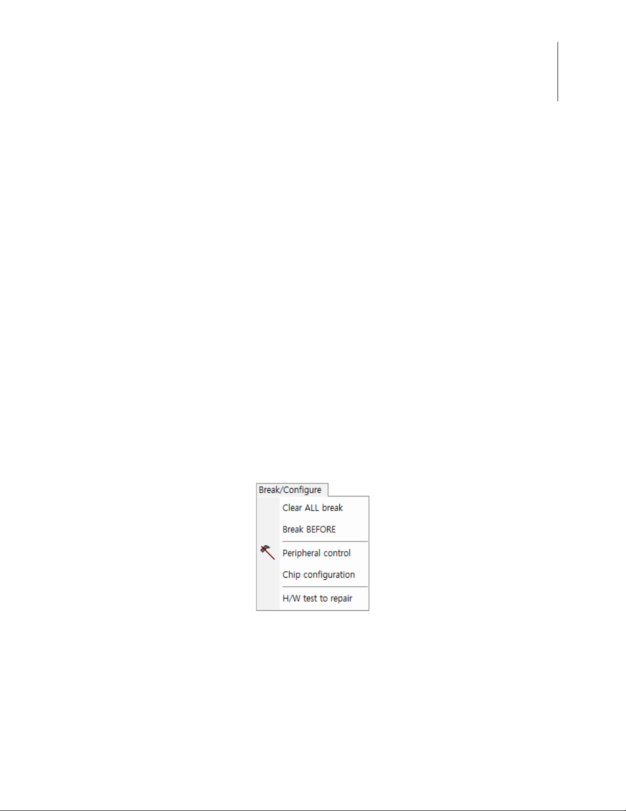
Break BEFORE (AFTER)
The Break BEFORE (AFTER) function prompts the user to select a PC breakpoint event
either before or after execution. When selecting this menu option, the Break Control dialog box appears, prompting the user to choose one of these two conditions; see Figure 15.
18
Figure 15. Break Control Dialog
Selecting
Break before execution causes a PC breakpoint when the PC reaches the PC
breakpoint address; however, a PC breakpoint position will not be executed, as illustrated
in the timing diagram shown in Figure 16.
Figure 16. Break BEFORE Timing Diagram
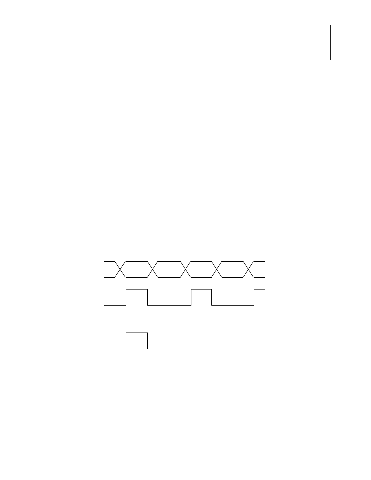
Selecting
break after execution causes a PC breakpoint to occur when the PC reaches the
PC breakpoint address, and a PC breakpoint position is executed, as illustrated in the tim-
UM024002-0512 The Z8051 On-Chip Debugger
ing diagram shown in Figure 17.
Page 27
Z8051 On-Chip Debugger and In-System Programmer
PC
Break
PC
PC+1 PC+2 PC+3
Fetch
signal
명령
opera
nd
명령
operand
Break
detect
Handl
e
User Manual
19
Figure 17. Break AFTER Timing Diagram
This Break BEFORE (AFTER) function is disabled (greyed out) in the Break/Configure
menu during emulation.
Peripheral Control
Selecting the Peripheral Control function from the Break/Configure menu prompts the
user to determine whether the target MCU’s internal peripheral functions should continue
to operate or remain idle, as shown in Figure 18. These peripherals are always running
during emulation by default.
Figure 18. Peripheral Control Dialog
The purpose of the Peripheral Control function is to tell the OCD whether the peripherals
UM024002-0512 The Z8051 On-Chip Debugger
should be stopped or continuously run during Break (Debug) Mode. All peripherals,
Page 28

Z8051 On-Chip Debugger and In-System Programmer
Note:
User Manual
including the PLL and ADC functions, will be stopped when selecting Stopped concur-
rently
. The Peripheral Control menu selection is disabled (greyed out) in the Break/Con-
figure menu during emulation.
The Peripheral Control function does not control each peripheral individually.
Chip Configuration
The Chip Configuration function is used to configure the target MCU’s I/O pin function,
oscillation method, code protection, etc. Each device series features different configurations. If a configuration changes, the user must turn off power to the target MCU, then
power it on again. As a result, configurations can be influenced when power rises to operational voltage.
20
The Configuration dialog box shown in Figure 19 offers an example con figu ration for the
Z51F0811 device.
Figure 19. Z51F0811 MCU Configuration Example
The Chip Configuration menu selection is disabled (greyed out) in the Break/Configure
menu during emulation.
UM024002-0512 The Z8051 On-Chip Debugger
Page 29

Z8051 On-Chip Debugger and In-System Programmer
User Manual
Hardware Test to Repair
The Hardware Test to Repair function is used for OCD emulator testing and repairing. Its
subfunctions are not available to the user.
View Menu
The View menu, shown in Figure 20, supports the opening of child windows. The Debugger offers the following nine types of child windows:
•
MCS51 basic registers
•
Code disassembly
•
Code dump
•
XDATA dump
21
•
IRAM dump
•
SFR dump
•
Watch Global
•
Watch Local
•
Text file
UM024002-0512 The Z8051 On-Chip Debugger
Page 30

Z8051 On-Chip Debugger and In-System Programmer
User Manual
22
Figure 20. The OCD’s View Menu
Each of the View menu’s functions are described in this section.
Toolbar
The Toolbar menu selection displays or hides the debugger’s toolbar. This toolbar is
located on the upper left side of the debugger frame. The toolbar displays frequently used
menu buttons for the user’s convenience.
Emulation Toolbar
This menu selection displays or hides the emulation toolbar, which is located to the right
of the main toolbar described above. The emulation toolbar displays frequently used emulation control menu buttons for the user’s convenience.
Window Open Bar
This menu selection displays or hides the window open bar, which is located to the right
side of the emulation toolbar described above. The window open bar displays menu buttons that can be used to open child windows.
UM024002-0512 The Z8051 On-Chip Debugger
Page 31

Z8051 On-Chip Debugger and In-System Programmer
User Manual
Status Bar
This menu selection displays or hides the status bar, which is located at the bottom of the
debugger frame. The status bar displays simple help features, the emulation clock count,
etc.
Z8051 Basic Registers
This menu selection opens a window that displays the Z8051 Series’ basic registers. If this
window is already open, selecting the
dow to appear at the top-most level of the debugger frame. See Figure 21.
Z8051 Basic Registers option will cause this win-
23
Figure 21. The Basic Registers Dialog
The Z8051 Basic Registers menu selection is disabled (greyed out) in the View menu during emulation.
Code Disassembly
This menu selection opens a window which displays the memory spaces containing disassembled code. If this window is already open, selecting
View menu will cause this window to appear at the top-most level of the debugger frame.
See the example in Figure 22.
UM024002-0512 The Z8051 On-Chip Debugger
Code Disassemble from the
Page 32

Z8051 On-Chip Debugger and In-System Programmer
User Manual
24
Figure 22. Code Disassembler Dialog
The Code Disassemble menu selection is disabled (greyed out) in the View menu during
emulation.
Code Dump
This menu selection opens a window which displays the contents of code memory in a
dumped format. If this window is already open, selecting
menu will cause this window to appear at the top-most level of the debugger frame. See
the example in Figure 23.
Code Dump from the View
UM024002-0512 The Z8051 On-Chip Debugger
Page 33

Z8051 On-Chip Debugger and In-System Programmer
User Manual
25
Figure 23. Code Dump Dialog
The Code Dump menu selection is disabled (greyed out) in the View menu during emulation.
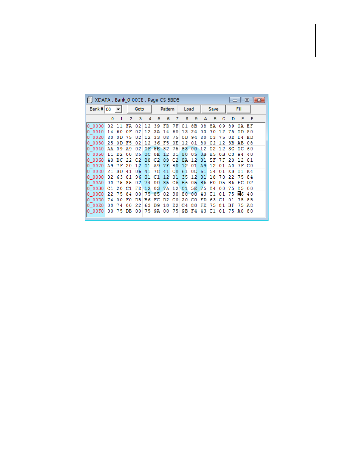
XDATA Dump
This menu selection opens a window which displays the contents of XDAT A memory in a
dumped format. The term XDATA refers to the external data memory contained in Z8051
Series devices. If this window is already open, selecting
menu will cause this window to appear at the top-most level of the debugger frame. See
the example in Figure 24.
XDATA Dump from the View
UM024002-0512 The Z8051 On-Chip Debugger
Page 34

Z8051 On-Chip Debugger and In-System Programmer
User Manual
26
Figure 24. XDATA Dump Dialog
The XDAT A Dump menu selection is disabled (greyed out) in the View menu during emulation.
IRAM Dump
This menu selection opens a window which displays the contents of IRAM memory in a
dumped format. The term IRAM refers to the internal data memory contained in Z8051
Series devices. If this window is already open, selecting
will cause this window to appear at the top-most level of the debugger frame. See the
example in Figure 25.
IRAM Dump from the View menu
UM024002-0512 The Z8051 On-Chip Debugger
Page 35

Z8051 On-Chip Debugger and In-System Programmer
User Manual
27
Figure 25. IRAM Dump Dialog
The IRAM Dump menu selection is disabled (greyed out) in the V iew menu during emulation.
SFR Dump
This menu selection opens a window which displays the contents of the SFR peripherals in
a dumped format. The term SFR refers to the special function registers contained in Z8051
Series devices. If this window is already open, selecting
will cause this window to appear at the top-most level of the debugger frame. See the
example in Figure 26.
SFR Dump from the View menu
UM024002-0512 The Z8051 On-Chip Debugger
Page 36

Z8051 On-Chip Debugger and In-System Programmer
Figure 26. SFR Dump Dialog
User Manual
28
The SFR Dump menu selection is disabled (greyed out) in the View menu during emulation.
Watch Global
This menu selection opens a window that displays global variables. If this window is
already open, selecting
appear at the top-most level of the debugger frame. See the example in Figure 27.
Watch Global from the View menu will cause this window to
Figure 27. Global Variables Dialog
The Watch Global menu selection is disabled (greyed out) in the View menu during emulation.
UM024002-0512 The Z8051 On-Chip Debugger
Page 37

Z8051 On-Chip Debugger and In-System Programmer
User Manual
Watch Local
This menu selection opens a window that displays local variables. If this window is
already open, selecting
appear at the top-most level of the debugger frame. See the example in Figure 28.
Watch Local from the Vi ew menu will cause this window to
29
Figure 28. Local Function Dialog
The Watch Local menu selection is disabled (greyed out) in the View menu during emulation.
Text File
This menu selection opens a window which displays the contents of a text file.
If a selected text file is already open, selecting
the window containing the text file to appear at the top-most level of the debugger frame;
otherwise, selecting
Text File will open a new window. See the example text file in
Figure 29.
Text File from the View menu will cause
UM024002-0512 The Z8051 On-Chip Debugger
Page 38

Z8051 On-Chip Debugger and In-System Programmer
User Manual
30
Figure 29. A Sample Text File
The Text File menu selection is disabled (greyed out) in the View menu during emulation.
UM024002-0512 The Z8051 On-Chip Debugger
Page 39

Z8051 On-Chip Debugger and In-System Programmer
Window Menu
The Window menu, shown in Figure 30, can be used to modify the arrangement of child
windows or to directly select a child window.
User Manual
31
Figure 30. The OCD’s Window Menu
UM024002-0512 The Z8051 On-Chip Debugger
Page 40

Z8051 On-Chip Debugger and In-System Programmer
User Manual
Cascade
This menu selection arranges opened child windows in a stepped visual sequence, as
shown in Figure 31.
32
Figure 31. Cascaded Windows
UM024002-0512 The Z8051 On-Chip Debugger
Page 41

Z8051 On-Chip Debugger and In-System Programmer
User Manual
Tile
This menu selection arranges opened child windows in a partitioned display, as shown in
Figure 32.
33
Figure 32. Tiled Windows
Close
This menu selection closes the top-most child window appearing in the debugger frame.
Windows 1, 2, 3, Etc.
This menu selection assigns a sequential number (e.g., 1, 2, 3…) to each child window in
the order in which it is opened. Users can directly select any open child window by its
number. In Figure 30
display the Code Disassembler window as the top-most window in the Debugger screen.
UM024002-0512 The Z8051 On-Chip Debugger
on page 31, for example, selecting 6 from the Window menu will
Page 42

Child Windows
Child windows are secondary windows that are displayed within the main OCD window.
Z8051 Basic Registers Window
The Z8051 Basic Registers window allows users to edit the contents of the Z8051 Series
registers. Figure 33 shows an example Z8051 Basic Registers window.
Z8051 On-Chip Debugger and In-System Programmer
User Manual
34
Figure 33. Using the Basic Registers Function, #1 of 6
Edit
The Modify button is disabled (greyed out) by default. Changing the value of a register
enables the
clicking the
In Figure 34, the current register bank is highlighted in the red area. Users can change register banks by selecting or deselecting any of the registers in this current register bank.
UM024002-0512 The Z8051 On-Chip Debugger
Modify button. New register values are downloaded to the target MCU upon
Modify button.
Page 43

Z8051 On-Chip Debugger and In-System Programmer
User Manual
35
Figure 34. Using the Basic Registers Function, #2 of 6
In Figure 35, the R0–R7 registers are highlighted in the red area. These registers map to
the same area as IRAM addresses in the range
00h–1Fh. Users can change these values by
entering 8-bit hexadecimal formats.
Figure 35. Using the Basic Registers Function, #3 of 6
UM024002-0512 The Z8051 On-Chip Debugger
Page 44

Z8051 On-Chip Debugger and In-System Programmer
User Manual
In Figure 36, the red area highlights the Program Status Word (PSW), in which bit units
can be changed.
36
Figure 36. Using the Basic Registers Function, #4 of 6
In Figure 37, the red area highlights the Accumulator (ACC), the B Register (B) and the
Stack Pointer (SP) registers. Enter a number in n 8-bit hexadecimal format to change any
of these values.
Figure 37. Using the Basic Registers Function, #5 of 6
UM024002-0512 The Z8051 On-Chip Debugger
Page 45

Z8051 On-Chip Debugger and In-System Programmer
User Manual
In Figure 38, the red area highlights the DPTR Register which displays, and can be edited
by, entering numbers in the 16-bit hexadecimal format. If the target MCU features more
than two DPTRs, the DPTR field in this dialog shows the currently selected register. If
each DPTR resides at a different address, Zilog recommends using the SFR window
instead.
37
Figure 38. Using the Basic Registers Function, #6 of 6
Code Disassemble Window
The Code Disassemble window displays the contents of code memory by using a disassemble format. All operand values must be entered in hexadecimal format. Figure 39
shows an example Code Disassembler window.
UM024002-0512 The Z8051 On-Chip Debugger
Page 46

Z8051 On-Chip Debugger and In-System Programmer
User Manual
38
Figure 39. Using the Code Disassembler Function, #1 of 3
If map/symbol files are already loaded, the affected source lines are highlighted by boxes,
as shown in Figure 40. Double-click any of these highlighted boxes to open its source file
and move to the appropriate address line.
Figure 40. Using the Code Disassembler Function, #2 of 3
UM024002-0512 The Z8051 On-Chip Debugger
Page 47

Z8051 On-Chip Debugger and In-System Programmer
User Manual
Line Assemble
The Line Assemble function supports a line assembly function in which users can change
the code space with assembly language. This function can directly change the target MCU
code space, but it does not change the source program file.
With your mouse, move the cursor to a line that you wish to change, and right-click to
open an edit field for the contents of that line, as shown in Figure 41. Change the contents
of the line by entering an instruction, operand, etc., in hexadecimal format.
39
Figure 41. Using the Code Assembler Function, #3 of 3
PC Break Toggle
The target MCU’ s internal Program Counter (PC), sets or clears all PC breakpoint settings.
The PC breakpoint count differs in each device in the Z8051 Series; normally , eight breakpoints can be set. In Figure 42, the red line represents a program counter breakpoint in the
line, and the blue line represents the current program counter.
UM024002-0512 The Z8051 On-Chip Debugger
Page 48

Z8051 On-Chip Debugger and In-System Programmer
User Manual
40
Figure 42. Using the PC Break Toggle Function
To set or clear a PC breakpoint, set your cursor on a selected line and double-click the
mouse’s left button.
Code Dump Window
Code dump windows display each 8-bit segment of code memory in the hexadecimal format and supports the editing of this data. Each 256-byte page resides at an address in the
range
xx00–xxFFh, in which xx is the number of the page.
The upper side of the Code Dump window displays the address of the current cursor position and the checksum of the current page. The current page number is displayed as a
watermark in the center of this window. In Figure 43, for example, the page number is
00.
UM024002-0512 The Z8051 On-Chip Debugger
Page 49

Z8051 On-Chip Debugger and In-System Programmer
User Manual
41
Figure 43. Using the Code Dump Function, #1 of 2
Edit
Users can change data values in the Code Dump window at any time, except during emulation. The editing method is quite simple; just place the cursor where you wish to make
an edit, and write a new character pair in hexadecimal format. The color of the character
pair will change from black to red to indicate that the change was made, as highlighted in
Figure 44.
UM024002-0512 The Z8051 On-Chip Debugger
Page 50

Z8051 On-Chip Debugger and In-System Programmer
User Manual
42
Figure 44. Using the Code Dump Function, #2 of 2
If you wish to cancel your inputs, press the Escape (Esc) key. Press the Enter key to save
your changes, and note that the red color of your changed character pair has changed back
to black.
Bank
The devices in the Z8051 Series use a linear addressing method, and display page units in
the 64 KB range. To overcome this 64 KB limit, the user can employ banked addresses, in
which a bank is the upper 4 bits of a 20-bit address.
Goto
Click the Goto button to view memory locations in any 16-bit segments within the
0000h–FFFFh address range in the Code Dump window or edit these memory locations
by entering an address in hexadecimal format. See the example Input dialog in Figure 45.
UM024002-0512 The Z8051 On-Chip Debugger
Page 51

Z8051 On-Chip Debugger and In-System Programmer
Figure 45. The Code Dump Function’s Goto/Input Dialog
Load
User Manual
43
Click the Load button to display the Pattern Load dialog, in which you can load a data pattern or code hex file to the code space; see Figure 46.
Figure 46. The Code Dump Function’s Pattern Load Dialog
Alternatively, users can download code by choosing
Load Hex from the File menu. How-
ever, this method is used to load user-specified data patterns only; it does not clear the
entire code space. A data pattern can be either a small code segment or complete program
code.
Save
Click the Save button to display the Pattern Save dialog, in which you can save a code
space as a pattern file; see the example in Figure 47.
UM024002-0512 The Z8051 On-Chip Debugger
Page 52

Z8051 On-Chip Debugger and In-System Programmer
Figure 47. The Code Dump Function’s Pattern Save Dialog
Fill
User Manual
44
Click the Fill button to display the Pattern Fill dialog, in which you can write a common
value in all code memory spaces in a specified address range; see the example in
Figure 48.
Figure 48. The Code Dump Function’s Pattern Fill Dialog
XDATA Dump Window
The XDATA Dump window displays each 8-bit segment of code memory in the hexadecimal format and supports the editing of this data. Each 256-byte page resides at an address
in the range
The upper side of the XDATA Dump window displays the address of the current cursor
position and the checksum of the current page. The current page number is displayed as a
watermark in the center of this window. In Figure 49, for example, the page number is
xx00–xxFFh, in which xx is the number of the page.
00.
UM024002-0512 The Z8051 On-Chip Debugger
Page 53
Z8051 On-Chip Debugger and In-System Programmer
User Manual
45
Figure 49. Using the XDATA Dump Function, #1 of 2
Edit
Users can change data values in the Code Dump window at any time, except during emulation. The editing method is quite simple; just place the cursor where you wish to make
an edit, and write a new character pair in hexadecimal format. The color of the character
pair will change from black to red to indicate that the change was made, as highlighted in
Figure 50.
UM024002-0512 The Z8051 On-Chip Debugger
Page 54

Z8051 On-Chip Debugger and In-System Programmer
User Manual
46
Figure 50. Using the XDATA Dump Function, #2 of 2
Bank
The devices in the Z8051 Series use a linear addressing method, and display page units in
the 64 KB range. To overcome this 64 KB limit, the user can employ banked addresses, in
which a bank is the upper 4 bits of a 20-bit address.
Goto
Click the Goto button to view memory locations in any 16-bit segments within the
0000h–FFFFh address range in the XDATA Dump window or edit these memory loca-
tions by entering an address in hexadecimal format. See the example in Figure 51.
Figure 51. The XDATA Dump Function’s Goto/Input Dialog
UM024002-0512 The Z8051 On-Chip Debugger
Page 55

Z8051 On-Chip Debugger and In-System Programmer
User Manual
Load
Click the Load button to display the Pattern Load dialog, in which you can load a data pattern or code hex file to the XDATA area. However, this command does not clear the
XDATA area; see Figure 52.
Figure 52. The XDATA Dump Function’s Pattern Load Dialog
47
Save
Click the Save button to display the Pattern Save dialog, in which you can save the
XDATA area as a pattern file; see Figure 53.
Figure 53. The XDATA Dump Function’s Pattern Save Dialog
Fill
Click the Fill button to display the Pattern Fill dialog, in which you can write a common
value in all XDATA memory spaces in a specified address range; see the example in
Figure 54.
UM024002-0512 The Z8051 On-Chip Debugger
Page 56

Figure 54. The XDATA Dump Function’s Pattern Fill Dialog
IRAM Dump Window
Z8051 On-Chip Debugger and In-System Programmer
User Manual
48
The IRAM Dump window displays each 8-bit segment of code memory in the hexadecimal format and supports the editing of this data. Each 256-byte page resides at an address
in the range
xx00–xxFFh, in which xx is the number of the page.
The upper side of the IRAM Dump window displays the addre s s of the curre nt cu rsor
position and the checksum of the current page. A watermark, displayed as
iR, appears in
the center of this window, as shown in Figure 55.
Figure 55 also shows IRAM addresses in the range
00h–7Fh, which represent the direct
area; the characters representing these addresses are colored black. IRAM addresses in the
range
80h–FFh represent the indirect area; these characters are colored cyan.
UM024002-0512 The Z8051 On-Chip Debugger
Page 57

Z8051 On-Chip Debugger and In-System Programmer
User Manual
49
Figure 55. Using the IRAM Dump Function, #1 of 2
To learn more about direct and indirect memory areas, please refer to the product specification for your particular Z8051 device.
Edit
Users can change data values in the IRAM Dump window at any time, except during emulation. The editing method is quite simple; just place the cursor where you wish to make
an edit, and write a new character pair in hexadecimal format. The color of the character
pair will change from black to red to indicate that the change was made, as highlighted in
Figure 56.
UM024002-0512 The Z8051 On-Chip Debugger
Page 58

Z8051 On-Chip Debugger and In-System Programmer
User Manual
50
Figure 56. Using the IRAM Dump Function, #2 of 2
If you wish to cancel your inputs, press the Escape (Esc) key. Press the Enter key to save
your changes, and note that the red color of your changed character pair has changed back
to black.
Save
Click the Save button to save the IRAM area as a pattern file.
SFR Dump Window
The Special Function Register (SFR) Dump window displays each 8-bit segment of code
memory in the hexadecimal format and supports the editing of this data. The upper side of
the SFR Dump window displays the address of the current cursor position and the checksum of the current page.
Figure 57 shows SFR addresses in the range
IRAM.
80h–FFh, which represent the direct area of
UM024002-0512 The Z8051 On-Chip Debugger
Page 59

Z8051 On-Chip Debugger and In-System Programmer
Figure 57. Using the SFR Dump Function, #1 of 3
User Manual
51
The special function registers differ in each Z8051 Series device. To learn more about special function registers, please refer to the product specification for your particular Z8051
device.
Edit
Users can change data values in the SFR Dump window at any time, except during emulation. The editing method is quite simple; just place the cursor where you wish to make an
edit, and write a new character pair in hexadecimal format. The color of the character pair
will change from black to red to indicate that the change was made, as highlighted in
Figure 58.
Figure 58. Using the SFR Dump Function, #2 of 3
UM024002-0512 The Z8051 On-Chip Debugger
Page 60

Z8051 On-Chip Debugger and In-System Programmer
User Manual
If you wish to cancel your inputs, press the Escape (Esc) key. Press the Enter key to save
your changes, and note that the red color of your changed character pair has changed back
to black.
Refresh
The SFR area includes static registers such as a stack pointer, an accumulator, etc. However, most SFRs are dynamic registers such as timers, I/Os, etc. Clicking the
ton (highlighted in Figure 59) redisplays all current data.
Refresh but-
52
Figure 59. Using the SFRDump Function, #3 of 3
Save
Clicking the Save button saves an SFR area as a pattern file.
Watch Global Window
The Watch Global window displays and supports the modification of global variables
within the user’s C language-based source program. Each variable is located within the
Code, XDATA, IRAM, SFR dump spaces. If users could easily determine a variable’s
location, they could edit the variable directly. However, finding a global variable across
these many memory dump spaces is often perceived to be a tedious process.
The Watch Global window alleviates this problem by employing a map/symbol file; see
Figure 60.
UM024002-0512 The Z8051 On-Chip Debugger
Page 61

Z8051 On-Chip Debugger and In-System Programmer
User Manual
53
Figure 60. The Watch Global Function’s Global Variables Dialog
Add Symbol
Clicking the Add Symbol button displays the Global Symbol Add/Remove dialog, in
which you can add a global variable to the Watch Global display list, shown in Figure 61.
Figure 61. Adding A Global Symbol
Remove Symbol
Clicking the Remove Symbol button removes a global variable from the Watch Global
display list.
UM024002-0512 The Z8051 On-Chip Debugger
Page 62

Z8051 On-Chip Debugger and In-System Programmer
User Manual
Edit
Users can change data values in the W atch Gl obal window at any time, except during emu lation. This editing method is quite simple; just place the cursor where you wish to make
an edit, and double-click the left button on your mouse to display a pop-up dialog in which
you can change the data and click the
shown in Figure 62.
Modify pop-up button to incorporate the change, as
54
Figure 62. Editing A Global Symbol
Watch Local Window
The Watch Global window displays and supports the modification of local variables
within the user’s C language-based source program. Each variable is located within the
Code, XDATA, IRAM, SFR dump spaces.
Much like the issue with finding global variables, users could edit these local variables
directly if finding them was not so tedious. The Watch Local window, shown in Figure 63,
alleviates this problem by employing a map/symbol file, as described in the previous section.
UM024002-0512 The Z8051 On-Chip Debugger
Page 63

Z8051 On-Chip Debugger and In-System Programmer
Figure 63. The Watch Local Function Dialog
User Manual
55
Edit
Users can change data values in the Watch Local window at any time, except during emulation. This editing method is quite simple; just place the cursor where you wish to make
an edit, and double-click the left button on your mouse to display a pop-up dialog in which
you can change the data and click the
Modify pop-up button to incorporate the change, as
shown in Figure 64.
Figure 64. Editing A Local Symbol
Add or Remove Symbol
Locals variables are dynamic; therefore, adding or removing a symbol will depend on
each program module.
In the Debugger, the user can check the current C module and find its local variables automatically so that the user is not required to add or remove the symbol.
UM024002-0512 The Z8051 On-Chip Debugger
Page 64

Z8051 On-Chip Debugger and In-System Programmer
User Manual
Figure 65 shows an example C source program module. The current program counter is
located in the
delay(UINT uCnt) function module (highlighted in the upper half of the
figure), and the Local Variable window displays the name of the module and its variable
(highlighted in the lower half of the figure).
56
Figure 65. Example Watch Local Function, #1 of 2
UM024002-0512 The Z8051 On-Chip Debugger
Page 65

Z8051 On-Chip Debugger and In-System Programmer
User Manual
If program flow is changed to another module, then the Local Variable list will be
changed, as shown in Figure 66.
57
Figure 66. Example Watch Local Function, #2 of 2
Text File Window
The Text File window displays text files, but does not support the editing of text files. If
you have loaded a map/symbol file, the source program file will display an actual hardware address in the line number area. To provide a visual understanding of this displayed
data, the following two examples offer a comparison.
Example 1. If a map/symbol file has not been loaded, or if the file does not include sym-
bol information, only the line number is displayed, as highlighted in Figure 67.
UM024002-0512 The Z8051 On-Chip Debugger
Page 66

Z8051 On-Chip Debugger and In-System Programmer
User Manual
58
Figure 67. Using the Text File Function, #1 of 5
Example 2. If a map/symbol file has been loaded and the file includes symbol informa-
tion, then the line number and address are displayed, as highlighted in Figure 68.
Figure 68. Using the Text File Function, #2 of 5
UM024002-0512 The Z8051 On-Chip Debugger
Page 67

Z8051 On-Chip Debugger and In-System Programmer
User Manual
Goto Line
Clicking the Goto Line button displays the Get Decimal Number dialog box, which
allows users to jump to another line in a text file; see Figure 69. Map/symbol information
is not required.
Figure 69. Using the Text File Function, #3 of 5
59
Disassemble Window Linkage
If a map/symbol file has been loaded and a text file is displayed (see the example in
Figure 70), the text file will show addresses instead of line numbers. In this Text File
Child Window, and with your mouse, set your cursor in an address area (the left-most column) and double-click the left button to launch the Code Disassemble dialog, which will
highlight the address.
UM024002-0512 The Z8051 On-Chip Debugger
Page 68

Z8051 On-Chip Debugger and In-System Programmer
User Manual
60
Figure 70. Text File Child Window
Example. Double-click the left button on your mouse at address 0_02C6. The Code Dis-
assembler child window appears, showing the
0_02C6 location at the top of the dialog;
see Figure 71.
UM024002-0512 The Z8051 On-Chip Debugger
Page 69

Z8051 On-Chip Debugger and In-System Programmer
User Manual
61
Figure 71. Code Disassembler Child Window
Break Toggle
If a map/symbol file has been loaded and a text file is displayed, the text file will show
addresses instead of line numbers. With your mouse, set your cursor in the text area and
double-click the left button to toggle all PC breakpoints.
UM024002-0512 The Z8051 On-Chip Debugger
Page 70

Z8051 On-Chip Debugger and In-System Programmer
User Manual
Figure 72 shows an example of a segment of source code in which the color of the PC
breakpoint line is red.
62
Figure 72. Using the Text File Function, #4 of 5
UM024002-0512 The Z8051 On-Chip Debugger
Page 71

Z8051 On-Chip Debugger and In-System Programmer
In Figure 73, the color of the current program counter address line is blue.
User Manual
63
Figure 73. Using the Text File Function, #5 of 5
UM024002-0512 The Z8051 On-Chip Debugger
Page 72

Z8051 On-Chip Debugger and In-System Programmer
Note:
User Manual
The Z8051 OCD In-System Programmer
The Z8051 On-Chip Debugger (OCD) In-System Programmer (ISP) has been developed
to support Zilog’s Z8051 8-bit MCUs. This document describes how to set up and use the
Z8051 On-Chip Debugger ISP with your Z8051 Development Kit. The OCD ISP is used
to program the Flash or EEPROM memory spaces of a target Z8051 MCU using Zilog’s
On-Chip Debugger. The OCD interface uses only two I/O lines
socket adapter or specified power circuit. An example ISP screen is shown in Figure 74.
1
and does not require a
64
Figure 74. Example On-Chip Debugger ISP Screen
If your system VCC is lower than device specifications, the OCD cannot program the
device.
1. The Z8051 OCD ISP requires a two-connection pin in your target system.
UM024002-0512 The Z8051 OCD In-System Programmer
Page 73

Z8051 On-Chip Debugger and In-System Programmer
Features
The key features of the Z8051 On-Chip Debugger ISP are:
•
Supports Zilog’s 8-bit Z8051 Family of MCUs
•
Uses the Intel HEX file format
•
Display the Code and XData areas in an editable hexadecimal dump format
•
Display and edit device configurations
•
Autodetects target devices
•
Can program eight devices simultaneously
•
Performs post-programming device verification
•
Supports all programming functions
User Manual
65
Connect the Hardware
After installing the OCD software and drivers, hardware connections can be established.
The pin positions of the Z8051 USB OCD interface are shown in Figure 75. Confirm the
target device’s pin positioning, and connect this interface to the USB port of your PC.
21
43 2
65 4 GND
87 6
10 9 8
Figure 75. OCD Hardware ISP Pin Assignment (Bottom View)
Pin No. Function
V<SubscriptTable>CC
OCD
S<SubscriptTable>CLK
OCD
S<SubscriptTable>DATA
UM024002-0512 The Z8051 OCD In-System Programmer
Page 74

Apply Power
Caution:
Observe the following procedure to complete your hardware connection to the Z8051
USB OCD interface.
1. Ensure that the power is off to the target MCU and that the MCU is soldered properly
onto the target board.
If your target MCU is already powered on prior to connecting the USB OCD interface,
it may not be able to recognize which mode the OCD is operating in. The target MCU is
identified at power-up whether it is in OCD or User Mode.
2. Power on your PC.
Z8051 On-Chip Debugger and In-System Programmer
User Manual
66
3. Connect the OCD hardware to your PC.
4. Connect the OCD hardware to your target system.
5. Apply power to the target system.
6. Use the OCD In-System Programmer to perform your programming tasks.
7. When your programming work is complete, power off the target system.
Understanding the OCD ISP Menu Functions
This section describes the operation of the HexData, Program, Window and Child menus.
HexData Menu
The HexData menu, shown in Figure 76, allows users to load their hexadecimal code to a
target device for programming. Because each device operates on its own programming
algorithm and features a different memory map, ISP functions are enabled only after a target device has been selected.
UM024002-0512 The Z8051 OCD In-System Programmer
Page 75

Z8051 On-Chip Debugger and In-System Programmer
User Manual
67
Figure 76. The OCD ISP’s File Menu
Select Device
Observe the following procedure to select a target device.
1. Run the Z8051 ISP software. Navigate via the Windows
Zilog Z8051 Software and Documentation <version_number> → Zilog Z8051
→
ISP <version_number>
2. From the
HexData menu of the ISP, choose Select Device. The Device Select dialog
.
box appears and displays a list of potential target devices, as shown in Figure 77.
Start menu to All Programs
UM024002-0512 The Z8051 OCD In-System Programmer
Page 76

Z8051 On-Chip Debugger and In-System Programmer
Note:
User Manual
68
Figure 77. Device Select Dialog
Load Code HEX File
Observe the following procedure to load and read a hexadecimal data file.
All hexadecimal files follow the Intel HEX format.
UM024002-0512 The Z8051 OCD In-System Programmer
Page 77

Z8051 On-Chip Debugger and In-System Programmer
Note:
User Manual
1. Select Load Code HEX File from the HexData menu to load a hexadecimal file from
the host PC to a code buffer space generated by the In-System Programmer. The Fill
Buffer dialog appears, as shown in Figure 78.
Figure 78. Fill Buffer Dialog
69
Loading a hexadecimal file into this code buffer space does not affect the memory space of
the target device.
The Fill Buffer dialog prompts the user to enter starting and ending addresses that
define the range of the code buffer space, plus the data pattern to fill the buffer space
before loading the hexadecimal file.
– Clicking the
Fill button performs the task of filling the code buffer with specified
data values.
– Clicking the
Don’t Care button will cause the buffer to remain loaded with the
data values that it currently contains.
– Clicking the
Cancel button cancels the file loading tasks and closes the Fill Buffer
dialog.
2. Click either the
Fill button or the Don’t Care button to open the File Open dialog box,
which is shown in Figure 79. Next, select the hexadecimal file that you wish to load
into the buffer, and click
Open.
UM024002-0512 The Z8051 OCD In-System Programmer
Page 78

Z8051 On-Chip Debugger and In-System Programmer
User Manual
70
Figure 79. File Open Dialog
3. The OCD_ISP dialog box appears, as shown in Figure 80. After a hexadecimal file
has been loaded, this dialog displays the name of the target device and a data check-
sum value, as highlighted in the figure.
UM024002-0512 The Z8051 OCD In-System Programmer
Page 79

Z8051 On-Chip Debugger and In-System Programmer
Note:
User Manual
71
Figure 80. OCD ISP Dialog
The ISP cannot calculate the checksum without a defined code buffer range (see Step 1).
Therefore, if you have not yet selected a target device yet, the Checksum field will display
????.
Load XData HEX File
Selecting Load XData HEX File from the HexData menu loads a hexadecimal file from
the host PC to the XData buffer of the ISP software; this hexadecimal file is in Intel HEX
format. Loading this file to the XData buffer space does not affect the memory space of
the target device.
UM024002-0512 The Z8051 OCD In-System Programmer
Page 80

Z8051 On-Chip Debugger and In-System Programmer
User Manual
Read Device
Selecting Load XData HEX File from the HexData menu causes the target device to be
read by the OCD hardware. When the host PC detects two or more hardware devices, it
prompts the user to select which device to read, as indicated in Figure 81.
72
Figure 81. Select Device To Read Dialog
If the selected target device is unlocked, the OCD hardware will read the code, XData and
configuration values, then update the display and the checksum.
If the selected target device is locked, the OCD hardware will display the term
LOCK and
prompt the user to read the configuration only.
Most Recent Files
As the user opens and closes files, these files will appear in the Hex Data menu, and can be
selected at any time in a current or future session. The maximum number of most recentlyused files that will appear in the Hex Data menu is eight. See the example in Figure 82,
which shows that the user has recently opened only three files; the third file (selected in
the figure) is the demo.hex file.
UM024002-0512 The Z8051 OCD In-System Programmer
Page 81

Z8051 On-Chip Debugger and In-System Programmer
User Manual
73
Figure 82. Most Recently Used Files
Exit
Choosing Exit from the HexData menu immediately terminates the OCD ISP.
Program Menu
The Program menu, shown in Figure 83, lists all of the OCD ISP’s programming main
control functions, each of which is described in this section. This menu is enabled after the
user selects a target device.
Figure 83. The OCD ISP’s Program Menu
UM024002-0512 The Z8051 OCD In-System Programmer
Page 82

Z8051 On-Chip Debugger and In-System Programmer
User Manual
Write
Selecting Write from the Program menu applies the entire programming sequence. This
sequence is listed below.
1. The host PC detects the OCD hardware and its connection with the target device.
2. All connected target devices are processed simultaneously.
3. The ISP erases the target device with a bulk erase algorithm.
4. The ISP next programs the code area.
5. The ISP verifies the code area.
6. The ISP programs the configuration area.
7. The ISP verifies the configuration area.
74
Verify
Selecting Verify from the Program menu initiates a comparison of the contents of the ISP
programmer’s buffer with the contents of the target device’s memory. This verification
sequence is described below.
1. The host PC detects the OCD hardware and its connection with the target device.
2. All connected target devices are processed simultaneously.
3. The ISP checks whether the target device is locked or unlocked. If the target is locked,
verification is canceled.
4. The ISP verifies the code area.
5. The ISP verifies the configuration area.
Erase
Selecting Erase from the Program menu causes the entire contents of the target device’s
memory, including configurations, to be erased. This erasure sequence is described below.
1. The host PC detects the OCD hardware and its connection with the target device.
2. All connected target devices are processed simultaneously.
3. The ISP erases the target device, whether it is locked or unlocked.
Blank Check
The Blank Check function determines if the target device is blank (entirely erased) after an
erasure. The sequence of this Blank Check function is described below.
1. The host PC detects the OCD hardware and its connection with the target device.
2. All connected target devices are processed simultaneously.
UM024002-0512 The Z8051 OCD In-System Programmer
Page 83

Z8051 On-Chip Debugger and In-System Programmer
User Manual
3. The ISP checks whether the target device is locked or unlocked. If the target is locked,
the Blank Check function is canceled.
4. The ISP determines if the code area is entirely erased.
5. The ISP determines if the configuration area is entirely erased.
Set Configuration
Because each device in the Z8051 Series is configured differently, use the Set Configuration function to configure the target device’s I/O pin functions, oscillation method, code
protection, etc.; see Figure 84 for an example.
75
Figure 84. Configuration Dialog
Window Menu
The Window menu, shown in Figure 85, can be used to modify the arrangement of child
windows or to directly select a child window.
UM024002-0512 The Z8051 OCD In-System Programmer
Page 84

Figure 85. The OCD ISP’s Window Menu
Open CODE Dump
Z8051 On-Chip Debugger and In-System Programmer
User Manual
76
Selecting Open CODE Dump from the Window menu opens a window which displays
code memory in a dump format, as shown in Figure 86. If this window is already open, the
window will move to the top-most level of the debugger frame.
Figure 86. Open CODE Dump Child Window
UM024002-0512 The Z8051 OCD In-System Programmer
Page 85

Z8051 On-Chip Debugger and In-System Programmer
User Manual
Open XData Dump
Selecting Open XData Dump from the W indow menu opens a window whi ch d isplays all
external data (XData) memory in a dump format. An example is shown in Figure 87. If
this window is already open, the window will move to the top-most level of the debugger
frame.
77
Figure 87. Open XData Dump Child Window
UM024002-0512 The Z8051 OCD In-System Programmer
Page 86

Z8051 On-Chip Debugger and In-System Programmer
User Manual
Cascade
Selecting Cascade from the Window menu arranges opened child windows in a stepped
(cascading) visual display, as shown in Figure 88.
78
Figure 88. Cascading Child Windows
UM024002-0512 The Z8051 OCD In-System Programmer
Page 87

Z8051 On-Chip Debugger and In-System Programmer
User Manual
Tile
Selecting Tile from the Window menu arranges opened child windows in a partitioned
(tiled) display, as shown in Figure 89.
79
Figure 89. Tiled Child Windows
Close
Selecting Close from the Window menu closes the top-most child window that appears in
the frame.
Windows 1, 2, 3, Etc.
This menu selection assigns a sequential number (e.g., 1, 2, 3…) to each child window in
the order in which it is opened. Users can directly select any open child window by its
number. In Figure 85
display the XData Dump window as the top-most window in the debugger screen.
on page 76, for example, selecting 2 from the Window menu will
Child Windows
Child windows are secondary windows that are displayed within the main ISP window.
The OCD ISP presents two child windows – the Code dump and XData windows.
UM024002-0512 The Z8051 OCD In-System Programmer
Page 88

Z8051 On-Chip Debugger and In-System Programmer
User Manual
Code Dump Window
Code dump windows display each 8-bit segment of code memory in the hexadecimal format and supports the editing of this data.
The upper side of the Code Dump window displays the address of the current cursor position. The term Code is displayed as a watermark in the center of this window, as shown in
Figure 90.
80
Figure 90. CODE Dump Child Window
Edit
Users can change data values in the Code Dump window at any time, except during programming execution. The editing method is quite simple: click the
Edit OK button ( ) appears, place the cursor where you wish to make an edit,
then write a new character pair in hexadecimal format. Upon changing any data, the
changed value will appear after a checksum is computed.
To disable a change of values, click the
Edit OK button so that the Edit NO button
( ) appears.
UM024002-0512 The Z8051 OCD In-System Programmer
Edit button so that the
Page 89

Z8051 On-Chip Debugger and In-System Programmer
User Manual
Cursor Position
The position of the cursor can be moved either by mouse click or by keystroke. If you prefer using your keyboard, use the arrow keys (up, down, left, right) and/or the PageUp,
PageDn, Home, and End keys. If you want to use your mouse, click the target position or
use the scroll bar.
XData Dump Window
The XDATA Dump window displays each 8-bit segment of code memory in the hexadecimal format and supports the editing of this data. Each 256-byte page resides at an address
in the range xx00–xxFFh, in which xx is the number of the page. The upper side of the
XDATA Dump window displays the address of the current cursor position. The term
XDATA is displayed as a watermark in the center of this window, as shown in Figure 91.
Editing and cursor functions are the same for the XDATA Dump window as they are for
the Code Dump window.
81
Figure 91. XData Dump Child Window
UM024002-0512 The Z8051 OCD In-System Programmer
Page 90

Z8051 On-Chip Debugger and In-System Programmer
User Manual
Appendix A. OCD Driver Installation on Windows Vista Systems
The driver programs for the Z8051 On-Chip Debugger are copied to the development PC
during the software and documentation installation. In the following procedure for PCs
running Windows Vista 32- and 64-bit operating systems, ensure that the target side of the
OCD will remain unconnected while you install these drivers.
1. Connect the OCD hardware to the USB port of your PC by connecting the A (male)
end of one of the two USB A (male)-to-Mini-B cables with the development PC’s
USB port. Connect the Mini-B end to the OCD device.
2. After the PC detects the new hardware, it will display the Found New Hardware Wiz-
ard dialog box, shown in Figure 92. Click
ommended)
.
Locate and install driver software (rec-
82
Figure 92. Found New Hardware Dialog, Windows Vista
3. Depending on your development PC’s User Account Control settings, Windows may
ask for permission to continue the installation. Click
UM024002-0512 The Z8051 OCD In-System Programmer
Continue.
Page 91

Z8051 On-Chip Debugger and In-System Programmer
User Manual
4. When the Insert the Disc dialog appears, as shown in Figure 93, select I don’t have
the disc. Show me other options.
Click the Next button to display the dialog that
follows, which is shown in Figure 94.
83
Figure 93. Install Device Driver Dialog, Windows Vista
UM024002-0512 The Z8051 OCD In-System Programmer
Page 92

Z8051 On-Chip Debugger and In-System Programmer
User Manual
84
Figure 94. Couldn’t Find Driver Dialog, Windows Vista
5. Return to page 6 and follow Steps 3 through 6.
UM024002-0512 The Z8051 OCD In-System Programmer
Page 93

Z8051 On-Chip Debugger and In-System Programmer
User Manual
Appendix B. OCD Driver Installation on Windows XP Systems
The driver programs for the Z8051 On-Chip Debugger are copied du ring the software and
documentation installation. On Windows XP systems, ensure that the targ et side of the
OCD will remain unconnected while you install these drivers. It is important that you
observe the following procedure; do not skip ahead until the OCD drivers are installed.
1. Connect the OCD hardware to the USB port of your PC by connecting the A-Male end
of one of the two USB A (male)-to-Mini-B cables with the host PC’s USB port, and
connect the Mini-B end to the OCD device.
85
2. After the PC detects the new hardware, it will display the
ard
dialog box, shown in Figure 95. Select Install from a list or specific location
(Advanced)
; then click Next.
Found New Hardware Wiz-
Figure 95. The Found New Hardware Wizard Welcome Screen
UM024002-0512 The Z8051 OCD In-System Programmer
Page 94

Z8051 On-Chip Debugger and In-System Programmer
Note:
User Manual
3. The next dialog box, shown in Figure 96, prompts you to enter a path or navigate to
the directory in which the
you use (32- bit or 64-bit), use the
paths and click the
Next button, leaving all other selections at their default settings.
.inf file was installed. Depending on the type of computer
Browse button to navigate to one of the following
– On 32-bit machines, use the following path:
<Z8051 Installation>\Z8051_<version_number>\device drivers\OCD USB\x32
– On 64-bit machines, use the following path:
<Z8051 Installation>\Z8051_<version_number>\device drivers\OCD USB\x64
On some installations, the Found New Hardware screen shown in Figure 95 may also display the text string,
Zilog Z8051 USB OCD - No Firmware. This occurrence is normal
and can be disregarded.
86
Figure 96. The Found New Hardware Wizard’s Browse Screen
UM024002-0512 The Z8051 OCD In-System Programmer
Page 95

Z8051 On-Chip Debugger and In-System Programmer
User Manual
4. When Windows prompts you whether to continue the installation or stop, click the
Continue Anyway button and wait until the installation is completed (Windows may
prompt you more than once). When the installation is complete, click
Finish.
87
UM024002-0512 The Z8051 OCD In-System Programmer
Page 96

Customer Support
To share comments, get your technical questions answered, or report issues you may be
experiencing with our products, please visit Zilog’s Technical Support page at http://sup-
port.zilog.com.
To learn more about this product, find additional documentation, or to discover other facets about Zilog product offerings, please visit the Zilog Knowledge Base
ticipating in the Zilog Forum
This publication is subject to replacement by a later edition. To determine whether a later
edition exists, please visit the Zilog website at http://www.zilog.com
.
Z8051 On-Chip Debugger and In-System Programmer
User Manual
88
or consider par-
.
UM024002-0512 Customer Support
 Loading...