

Page 1

ZNEO® Motor Control Family
Z16FMC™ Series Motor
Control Development Kit
User Manual
UM023402-0811
Copyright ©2011 Zilog®, Inc. All rights reserved.
www.zilog.com
Page 2

Z16FMC™ Series Motor Control Development Kit
Warning:
User Manual
ii
DO NOT USE THIS PRODUCT IN LIFE SUPPORT SYSTEMS.
LIFE SUPPORT POLICY
ZILOG’S PRODUCTS ARE NOT AUTHORIZED FOR USE AS CRITICAL COMPONENTS IN LIFE
SUPPORT DEVICES OR SYSTEMS WITHOUT THE EXPRESS PRIOR WRITTEN APPROVAL OF
THE PRESIDENT AND GENERAL COUNSEL OF ZILOG CORPORATION.
As used herein
Life support devices or systems are devices which (a) are intended for surgical implant into the body, or (b)
support or sustain life and whose failure to perform when properly used in accordance with instructions for
use provided in the labeling can be reasonably expected to result in a significant injury to the user. A critical component is any componen t in a li fe supp ort device o r syste m whose failure to p erform ca n be re asonably expected to cause the failure of the life support device or system or to affect its safety or effectiveness.
Document Disclaimer
©2011 Zilog, Inc. All rights reserved. Information in this publication concerning the devices, applications,
or technology described is intended to suggest possible uses and may be superseded. ZILOG, INC. DOES
NOT ASSUME LIABILITY FOR OR PROVIDE A REPRESENTATION OF ACCURACY OF THE
INFORMATION, DEVICES, OR TECHNOLOGY DESCRIBED IN THIS DOCUMENT. ZILOG ALSO
DOES NOT ASSUME LIABILITY FOR INTELLECTUAL PROPERTY INFRINGEMENT RELATED
IN ANY MANNER TO USE OF INFORMATION, DEVICES, OR TECHNOLOGY DESCRIBED
HEREIN OR OTHERWISE. The information contained within this document has been verified according
to the general principles of electrical and mechanical engineering.
Z8, Z8 Encore!, Z8 Encore! XP, Z8 Encore! MC, eZ80, ZNEO and Z16FMC are trademarks or registered
trademarks of Zilog, Inc. All other product or service names are the property of their respective owners.
Foreword UM023402-0811
Page 3

Revision History
Each instance in the Revision History table below reflects a change to this document from
its previous version. For more details, click the appropriate links in the table.
Revision
Date
Aug
2011
Nov
2010
Level Description Page
02 Updated schematic diagram in Figure 7 to Rev C per CR#13165. 13
01 Original issue. All
Z16FMC™ Series Motor Control Development Kit
User Manual
iii
UM023402-0811 Revision History
Page 4

Z16FMC™ Series Motor Control Development Kit
User Manual
iv
Revision History UM023402-0811
Page 5

Table of Contents
Revision History . . . . . . . . . . . . . . . . . . . . . . . . . . . . . . . . . . . . . . . . . . . . . . . . . . . . . . . .iii
Introduction . . . . . . . . . . . . . . . . . . . . . . . . . . . . . . . . . . . . . . . . . . . . . . . . . . . . . . . . . . . . 1
Kit Features . . . . . . . . . . . . . . . . . . . . . . . . . . . . . . . . . . . . . . . . . . . . . . . . . . . . . . . . . 1
Development Kit Block Diagram . . . . . . . . . . . . . . . . . . . . . . . . . . . . . . . . . . . . . . . . 1
MC MDS Module Description . . . . . . . . . . . . . . . . . . . . . . . . . . . . . . . . . . . . . . . . . . . . . 2
Module Features . . . . . . . . . . . . . . . . . . . . . . . . . . . . . . . . . . . . . . . . . . . . . . . . . . . . . 3
3-Phase Motor Control Application Board . . . . . . . . . . . . . . . . . . . . . . . . . . . . . . . . . . . 10
Application Board Features . . . . . . . . . . . . . . . . . . . . . . . . . . . . . . . . . . . . . . . . . . . 10
ZDS II . . . . . . . . . . . . . . . . . . . . . . . . . . . . . . . . . . . . . . . . . . . . . . . . . . . . . . . . . . . . . . . . 11
Z16FMC™ Series Motor Control Development Kit
User Manual
v
Troubleshooting and Developer Guidelines . . . . . . . . . . . . . . . . . . . . . . . . . . . . . . . . . . 11
Recheck Procedures with the Quick Start Guide . . . . . . . . . . . . . . . . . . . . . . . . . . . 12
Zilog Customer Support Contact . . . . . . . . . . . . . . . . . . . . . . . . . . . . . . . . . . . . . . . 12
Linix Motor Wiring Information . . . . . . . . . . . . . . . . . . . . . . . . . . . . . . . . . . . . . . . . . . . 12
Schematic Diagrams . . . . . . . . . . . . . . . . . . . . . . . . . . . . . . . . . . . . . . . . . . . . . . . . . . . . 13
Customer Support . . . . . . . . . . . . . . . . . . . . . . . . . . . . . . . . . . . . . . . . . . . . . . . . . . . . . . 19
UM023402-0811 Table of Contents
Page 6

Z16FMC™ Series Motor Control Development Kit
User Manual
vi
Table of Contents UM023402-0811
Page 7

Introduction
Zilog’s Z16FMC™ Series Motor Control Development Kit aids in the develoment of
motor control applications using Zilog’s 64-LQFP Z16FMC Motor Control MCU and pro vides an application-specific platform for creating a design based on the Z16FMC series
microcontroller. The development kit features a Motor Control Modular Development
System (MC MDS) module mounted on a 3-Phase Motor Control Application Board. A
24 VDC, 3200 RPM 3-phase motor is included with the kit.
Kit Features
The key features of the Z16FMC™ Series Motor Control Development Kit include:
•
Z16FMC™ Series Motor Control Development Kit
User Manual
1
MC MDS Module
•
3-Phase Motor Control Application Board
•
USB Smart Cable with opto-isolator
•
3-phase 24 VDC, 30 W , 3200 RPM motor with spade connectors and Internal Hall Sen-
sors (powered by external adjustable 24 VDC supply, not included in kit)
•
Universal 5 VDC power supply
•
Motor Control Software and Documentation CD-ROM
™
For Z16FMC
refer to the Z16FMC
(QS0079).
Series Motor Control Development Kit installation and setup instructions,
™
Series Motor Control Development Kit Quick Start Guide
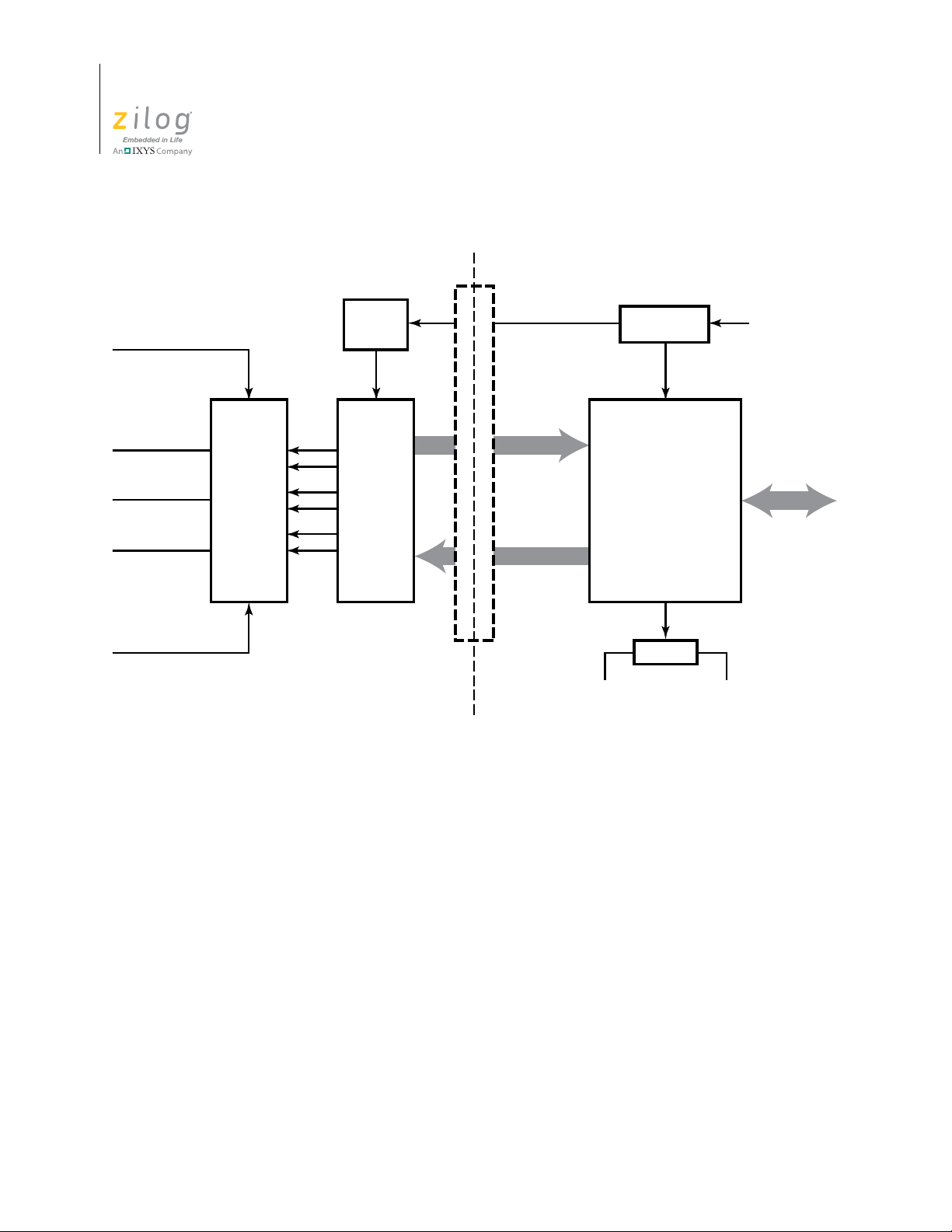
Development Kit Block Diagram
Figure 1 displays a block diagram of the Z16FMC™ Series Motor Control Development
Kit.
UM023402-0811 Introduction
Page 8
Z16FMC™ Series Motor Control Development Kit
3.3V to
12V
Converter
Gate Drivers
and
Sensors
Power
MOSFETs
Phase B
+24V, 1A
Analog Signals
AH
AL
BH
BL
CH
CL
PWM
Debug
Motor Control
MDS Module
Motor Control
Application Board
5 VDC
GND
3.3V Power
Regulator
Z16FMC MCU
Speed
User Manual
2
Figure 1. Z16FMC Series Motor Control Development Kit
MC MDS Module Description
The MC MDS Module features the Z16FMC MCU, as shown in Figure 2. It provides circuitry that interfaces the chip to an external development PC running the Zilog Developer
Studio II (ZDS II) Integrated Development Environment (IDE), and to the 3-Phase Motor
Control Application Board.
MC MDS Module Description UM023402-0811
Page 9

Z16FMC™ Series Motor Control Development Kit
User Manual
3
Module Features
The features of the MC MDS Module include:
•
A Z16FMC device operating at 20 MHz with 128 KB of internal Flash memory and
4 KB of internal register SRAM
•
20 MHz ceramic resonator Y1
•
Two SPDT switches, S2 and S3(labeled DIRECTION and STOP/RUN, respectively)
•
One 5 K potentiometer, R7
•
Green LED D1 (illuminates when 3.3 VDC is applied to the board)
•
Three general-purpose LEDs D2, D3 and D4
•
RS-232 port
•
6-pin DBG interface
•
Two 60-pin headers for connecting to the 3-Phase Motor Control Application Board
(JP1 and JP2; JP1 used for physical mounting only)
Figure 2. MC MDS Module
UM023402-0811 MC MDS Module Description
Page 10

Z16FMC™ Series Motor Control Development Kit
User Manual
4
Z16FMC MCU
The Z16FMC Series Flash microcontrollers are based on Zilog’s advanced ZNEO 16-bit
CPU core. Optimized for motor control applications, these devices support the control of
single- and multi-phase variable-speed motors. Target applications are large appliances,
small appliances and HVAC.
™
The Z16FMC
present all the features of the Z16FMC MCU. The key features of the Z16FMC MCU
include:
•
16-bit optimized single-cycle CISC core
•
Up to 128 KB of in-circuit programmable Flash memory
•
Highly integrated digital/analog peripherals
– Operational Amplifier
– Analog Comparator
– Internal Precision Oscillator
– 4-Channel DMA Controller
– 12-bit PWM module with three complementary pairs or six independent PWM
outputs
Series Motor Control Development Kit consists of circuitry to support and
•
Flexible communication interface including a 9-bit UART with LIN and IrDA, I2C,
and ESPI
•
12-Channel, 10-bit ADC with a 2.1μs conversion time
For more information about the Z16FMC MCU, refer to the Z16FMC Series
trol Product Specification (PS0287) or the Z16FMC Series Flash Microcontroller Product
Brief (PB0229) available from the kit’s CD-ROM and also available for download at
www.zilog.com
.
Motor Con-
Connector JP2
Connector JP2 is a 60-pin header that connects I/O from the Z16FMC MCU to the 3-Phase
Motor Control Application Board. Figure 3 displays the pin layout. Table 1, which follows, identifies the signals and their functions.
MC MDS Module Description UM023402-0811
Page 11

Z16FMC™ Series Motor Control Development Kit
NC
NC
NC
NC
NC
NC
NC
NC
NC
NC
ANA7
PD5_TXD1
PC1_TOUT
ANA3
PC3_SCK
PWMH1
PC4_MOSI
GND
ANA5
PA7_SDA
PD3
PC6_T2IN_PWMH0
GND
VCC_3v3
PC7_T2OUT_PWML0
ANA4
GND
PWML2
PA2
PWMH2
PC2_nSS
ANA0
PA6_SCL
PD6_nCTS1
PA4_RXD0
PC0_T1IN
PWML1
ANA1
PC5_MISO
PA3_nCTS0
ANA2
PD4_RXD1
-RESET
VCC_3v3
VCC_3v3
GND
ANA6
PA5_TXD0
GND
PH3_ANA11
GND
PA0
PA1 PF7
PG3
PWMH2 PWML2
PWMH1
PWML1
TXD1
RXD1
nCTS1
-RESET
DE1
PF7
PG3
JP2
HDR/PIN 2x30
JP2
HDR/PIN 2x30
1
1
2
2
3
3
4
4
5
5
6
6
7
7
8
8
9
9
10
10
111112
12
131314
14
151516
16
171718
18
191920
20
212122
22
232324
24
252526
26
272728
28
292930
30
313132
32
333334
34
353536
36
373738
38
393940
40
414142
42
434344
44
454546
46
474748
48
494950
50
515152
52
535354
54
555556
56
575758
58
595960
60
User Manual
5
Figure 3. MC MDS Board Connector JP2
Table 1. Connector JP2 Signal Descriptions
Signal Pins
ANA0 1 I Analog input to the ADC.
ANA1 2 I Analog input to the ADC.
ANA2 3 I Analog input to the ADC.
ANA6 4 I Analog input to the ADC.
ANA7 5 I Analog input to the ADC.
ANA3 6 I Analog input to the ADC.
ANA4 7 I Analog input to the ADC.
ANA5 8 I Analog input to the ADC.
VCC_3v3 9 n/a 3.3 VDC Power.
GND 10 n/a Ground.
UM023402-0811 MC MDS Module Description
Direction
(with respect
to MCU) Description
Page 12

Z16FMC™ Series Motor Control Development Kit
User Manual
6
Table 1. Connector JP2 Signal Descriptions (Continued)
Direction
(with respect
Signal Pins
PC4_MOSI 11 I/O Port C[4]; used for general purpose I/O or MOSI.
PC5_MISO 12 I/O Port C[5]; used for general purpose I/O or MISO.
PWMH2 13 O PWM High Output.
PWML2 14 O PWM Low Output.
PC3_SCK 15 I/O Port C[3]; used for general purpose I/O or SCK.
PC2_nSS 16 I/O Port C[2]; used for general purpose I/O or nSS.
PWMH1 17 O PWM High Output.
PC6_T2IN_PWMH0 18 I/O Port C[6]; used for general purpose I/O or T2IN or
GND 19 n/a Ground.
PC7_TOUT_PWML0 20 I/O Port C[7]; used for general purpose I/O or TOUT or
PWML1 21 O PWM Low Output.
PA2 22 I/O Port A[2]; used for general purpose I/O.
PC1_TOUT 23 I/O Port C[1]; used for general purpose I/O or T1OUT.
PD6_nCTS1 24 I/O Port D[6]; used for general purpose I/O or nCTS1.
PD3 25 I/O Port D[3]; used for general purpose I/O.
PD4_RXD1 26 I/O Port D[4]; used for general purpose I/O or RXD1.
PD5_TXD1 27 I/O Port D[5]; used for general purpose I/O or TXD1.
PC0_T1IN 28 I/O Port C[0]; used for general purpose I/O or T1IN.
PA0 29 I/O Port A[0]; used for general purpose I/O.
GND 30 n/a Ground.
PA1 31 I/O Port A[1]; used for general purpose I/O.
PF7 32 I/O Port F[7]; used for general purpose I/O.
PA3_nCTS0 33 I/O Port A[3]; used for general purpose I/O or nCTS0.
PG3 34 I/O Port G[3]; used for general purpose I/O.
PA4_RXD0 35 I/O Port A[4]; used for general purpose I/O or RXD0.
PA5_TXD0 36 I/O Port A[5]; used for general purpose I/O or TXD0.
NC 37 n/a No Connect.
NC 38 n/a No Connect.
GND 39 n/a Ground.
NC 40 n/a No Connect.
to MCU) Description
PWMH0.
PWML0.
MC MDS Module Description UM023402-0811
Page 13

Z16FMC™ Series Motor Control Development Kit
User Manual
Table 1. Connector JP2 Signal Descriptions (Continued)
Direction
(with respect
Signal Pins
NC 41 n/a No Connect.
NC 42 n/a No Connect.
NC 43 n/a No Connect.
NC 44 n/a No Connect.
PA6_SCL 45 I/O Port A[6]; used for general purpose I/O or SCL.
GND 46 n/a Ground.
PA7_SDA 47 I/O Port A[7]; used for general purpose I/O or SDA.
GND 48 n/a Ground.
NC 49 n/a No Connect.
NC 50 n/a No Connect.
NC 51 n/a No Connect.
NC 52 n/a No Connect.
RESET 53 n/a SET is active Low.
PH3_ANA11 54 I/O Port H[3]; used for general purpose I/O or ANA11.
VCC_3v3 55 n/a 3.3 VDC Power.
GND 56 n/a Ground.
NC 57 n/a No Connect.
NC 58 n/a No Connect.
VCC_3v3 59 n/a 3.3 VDC Power.
NC 60 n/a No Connect.
to MCU) Description
7
UM023402-0811 MC MDS Module Description
Page 14

Z16FMC™ Series Motor Control Development Kit
VREF
PB5_ANA5
PB7_ANA7
PB3_ANA3
PB0_ANA0
PB6_ANA6
PB2_ANA2
PH0_ANA8
PB1_ANA1
PB4_ANA4
PH1_ANA9
PH2_ANA10
PH3_ANA11
JP3
HDR/PIN 2x13
JP3
HDR/PIN 2x13
1
1
2
2
3
3
4
4
5
5
6
6
7
7
8
8
9
9
10
10
111112
12
131314
14
151516
16
171718
18
191920
20
212122
22
232324
24
252526
26
User Manual
8
Connector JP3
Connector JP3 is a 26-pin header that allows access to the analog signals. Figure 4 displays the pin layout. Table 2, which follows, identifies the signals and their functions.
Figure 4. MC MDS Board Connector JP3
Table 2. Connector JP3 Signal Descriptions
Direction
(with respect
Signal Pins
V
REF
1 Input ADC Reference Voltage.
to MCU) Description
ANA11 3 Input Input to ADC.
ANA10 5 Input Input to ADC.
ANA2 7 Input Input to ADC.
ANA3 9 Input Input to ADC.
ANA7 11 Input Input to ADC.
ANA6 13 Input Input to ADC.
ANA5 15 Input Input to ADC.
ANA4 17 Input Input to ADC.
MC MDS Module Description UM023402-0811
ANA1 19 Input Input to ADC.
ANA0 21 Input Input to ADC.
ANA8 23 Input Input to ADC.
ANA9 25 Input Input to ADC.
GND 2, 4, 6, 8, 10, 12, 14, 16,
18, 20, 22, 24, 26
n/a Ground.
Page 15

Z16FMC™ Series Motor Control Development Kit
PE0
PE1
PE2
PE3
PE4
PE5
PE6
PE7
J1
HDR/PIN 2x8
J1
HDR/PIN 2x8
1 2
3 4
5 6
7 8
9 10
11 12
13 14
15 16
User Manual
Connector J1
Connector J1 is a 16-pin header that allows access to all Port E signals. Figure 5 displays
the pin layout. Table 3, which follows, identifies the Port E signals and their functions.
Figure 5. MC MDS Board Connector JP1
9
Table 3. Connector JP1 Signal Descriptions
Direction
(with respect
Signal Pins
to MCU) Description
PE0 1 I/O Port E[0].
PE1 3 I/O Port E[1].
PE2 5 I/O Port E[2].
PE3 7 I/O Port E[3].
PE4 9 I/O Port E[4].
PE5 11 I/O Port E[5].
PE6 13 I/O Port E[6].
PE7 15 I/O Port E[7].
GND 2, 4, 6, 8, 10, 12, 14, 16 n/a GND.
Jumper and Switch Settings
The MDS module has two SPDT switches (S2 and S3) and a 5 K potentiometer (R7) used
by the development kit’ s preloaded demonstration software to perform the following functions:
S2, DIRECTION. Used to change the 3-phase motor spin direction.
S3, STOP/RUN. Used to turn the 3-phase motor ON and OFF.
UM023402-0811 MC MDS Module Description
R7, SPEED. Used to adjust the 3-phase motor RPM.
Page 16

Z16FMC™ Series Motor Control Development Kit
User Manual
10
Physical Dimensions
The footprint of the MC MDS module PCB is 9.5 cm x 9.30 cm. When mounted on the 3Phase Motor Control Application Board, the overall development kit height is 4.0 cm.
3-Phase Motor Control Application Board
The 3-Phase Motor Control Application Board provides circuitry that drives the 3-phase
24 VDC, 3200 RPM motor included with the development kit (see Figure 6). It provides
fused 24 VDC inputs for supplying external adjustable workbench power to run the motor,
and interfaces the motor to the Z16FMC MCU mounted on the MC MDS module.
Figure 6. 3-Phase Motor Control Application Board
Application Board Features
The features of 3-Phase Motor Control Application Board include:
•
Three spade lug connectors, one for each motor phase
•
Dual power MOSFETs for each motor phase
3-Phase Motor Control Application Board UM023402-0811
Page 17

Z16FMC™ Series Motor Control Development Kit
User Manual
•
Heat sink temperature sensor
•
Spade lug connectors for power input from adjustable 24 VDC power source (for connection to 3-phase motor)
•
5 A fuse, F1
•
Two 60-pin headers for connection to the MC MDS Module (JP1 and JP2; JP1 used
for physical mounting only)
Power MOSFETs and Gate Drivers
Each of the phase outputs on spade lugs P1, P2, and P3 are driven by a pair of power
MOSFETs, one for the high side and one for the low side. A gate driver circuit is associated with each pair of power MOSFETs.
Fused External Power Interface
11
An interface to an adjustable 0 VDC to 24 VDC workbench power supply is provided
through spade lug connectors P4 (+) and P5 (–). The input power is fused through 5 A
3 AG fuse F1.
Physical Dimensions
The footprint of the 3-Phase Motor Control Application Board PCB is 12.44 cm x
12.44 cm. With the MC MDS module mounted on it, the overall development kit height is
4.31 cm.
ZDS II
The Zilog Developer Studio II (ZDS II) Integrated Development Environment (IDE) is a
complete stand-alone system that provides a state-of-the-art development environment.
Based on the Windows
language-sensitive editor, project manager, C-Compiler, assembler, linker, librarian, and
source-level symbolic debugger that supports the Z16FMC Series of devices.
®
XP/Vista-32/Win 2000-SP4 user interfaces, ZDS II integrates a
Troubleshooting and Developer Guidelines
Before contacting Zilog Customer Support to submit a problem report, follow the steps
below. If there is a hardware failure, contact a local Zilog representative for assistance.
UM023402-0811 ZDS II
Page 18

Z16FMC™ Series Motor Control Development Kit
User Manual
12
Recheck Procedures with the Quick Start Guide
Follow the procedures in the Z16FMC™ Series Motor Control Development Kit Quick
Start Guide (QS0079) – contained in the kit – and verify that the kit is set up as specified
in the document.
Zilog Customer Support Contact
For additional troubleshooting solutions, refer to ZDS II Online Help. For valuable infor-
mation about customer and technical support, as well as hardware and software development tools, visit the Zilog website at w
released versions of ZDS II.
Linix Motor Wiring Information
ww.zilog.com, where you’ll also find the latest
The Linix 3-phase motor included with the development kit provides three heavy-gauge
wires for phase connections and five light-gauge wires used to power and access internal
sensors, as indicated in Table 4.
Table 4. 3-Phase Motor Wiring Information
Wire Description
Heavy-gauge white wire Motor Phase A connection
Heavy-gauge blue wire Motor Phase B connection
Heavy-gauge green wire Motor Phase C connection
Light-gauge red wire Sensor power V
Light-gauge black wire Sensor power ground (-)
Light-gauge white wire Sensor signal S
Light-gauge blue wire Sensor signal S
Light-gauge green wire Sensor signal S
CC
A
B
C
(+)
Linix Motor Wiring Information UM023402-0811
Page 19

Schematic Diagrams
5
5
4
4
3
3
2
2
1
1
D D
C C
B B
A A
V+
PHASE_A PHASE_BPHASE_BPHASE_B PHASE_C
GATE_AH
GATE_AL GATE_BL
GATE_BH
GATE_CH
GATE_CL
+BUS+BUS+BUS+BUS+BUS+BUS+BUS+BUS+BUS+BUS+VDC +BUS+BUS+BUS+BUS+BUS+BUS+BUS+BUS+BUS+BUS
GND
TH
CS+
CS-
TH
Title
Size Document Number Rev
Date: Sheet
of
96C0960-001
C
3 PHASE MOTOR CONTROL APPLICATION BOARD
A
13Monday, April 26, 2010
Title
Size Document Number Rev
Date: Sheet
of
96C0960-001
C
3 PHASE MOTOR CONTROL APPLICATION BOARD
A
13Monday, April 26, 2010
Title
Size Document Number Rev
Date: Sheet
of
96C0960-001
C
3 PHASE MOTOR CONTROL APPLICATION BOARD
A
13Monday, April 26, 2010
3 PHASE POWER STAGE
HEATSINK TEMP SENSOR
AB C
R5
10.00kR510.00k
Q3
IXTP64N055T
Q3
IXTP64N055T
+
C4
3300uF 50V
+
C4
3300uF 50V
Q2
IXTP64N055T
Q2
IXTP64N055T
R4
NTC 10kR4NTC 10k
P5P5
P2P2
Q1
IXTP64N055T
Q1
IXTP64N055T
F1
5A FUSE
F1
5A FUSE
Q6
IXTP64N055T
Q6
IXTP64N055T
R6
150kR6150k
R3 10.0kR3 10.0k
C3
0.1uF 50V
C3
0.1uF 50V
Q5
IXTP64N055T
Q5
IXTP64N055T
C2
0.1uF 50V
C2
0.1uF 50V
P4P4
R2 10.0kR2 10.0k
+
C5
3300uF 50V
+
C5
3300uF 50V
P1P1
C1
0.1uF 50V
C1
0.1uF 50V
R1
0.100 OHM
R1
0.100 OHM
Q4
IXTP64N055T
Q4
IXTP64N055T
P3P3
Figures 7 through 9 display schematics for the 3-Phase Motor Control Application Board.
Z16FMC™ Series Motor Control Development Kit
User Manual
13
UM023402-0811 Schematic Diagrams
Figure 7. 3-Phase Motor Control Application Board Schematic, #1 of 3
Page 20

Z16FMC™ Series Motor Control Development Kit
5
5
4
4
3
3
2
2
1
1
D
D
C
C
B
B
A A
GATE DRIVE
BEMF DIVIDERS
12V SUPPLY
96C0960-001
B
3 PHASE MOTOR CONTROL APPLICATION BOARD
A
23Wednesday, June 08, 2005
Title
veRrebmuN tnemucoDeziS
teehS:etaD
of
GATE_AL
GATE_AH
PHASE_AAL
AH
PHASE_BBL
BH
GATE_BL
GATE_BH
PHASE_C
CH
GATE_CL
GATE_CH
PHASE_A PHASE_B PHASE_C
VAVA VBVBVBVB
CL
VCC_3.3V
VC
+12V
+12V
+12V
+12V
R10
150k
C6
10uF
R18 22.1
C19
10uF
C11
0.1uF
R12
150k
C13
10uF
R13 22.1
R20
86.6k
R7
10.00k
U2
IR2101
1
2
3
4
5
6
7
8
VCC
HIN
LIN
COM LO
VS
HO
VB
D3 BAV19
C12
0.1uF
L1
10uH
R15 22.1
R14 22.1
R9
10.00k
C14
10uF
C20
68pF
R11
10.00k
R16 22.1
U1
IR2101
1
2
3
4 5
6
7
8
VCC
HIN
LIN
COM LO
VS
HO
VB
C8
0.1uF
D4 BAV19
C17
10uF
D2 BAV19
C15
0.1uF
U3
IR2101
1
2
3
4
5
6
7
8
VCC
HIN
LIN
COM LO
VS
HO
VB
U4
TPS61041
1
2
3
4
5
SW
GND
FB
EN
VIN
R8
150k
D1 BAV19
C16
0.1uF
C18
10uF
C7
0.1uF
R17 22.1
C10
10uF
R19
10.0k
C9
10uF
User Manual
14
Figure 8. 3-Phase Motor Control Application Board Schematic, #2 of 3
Schematic Diagrams UM023402-0811
Page 21

Z16FMC™ Series Motor Control Development Kit
5
5
4
4
3
3
2
2
1
1
D
D
C
C
B
B
A
A
ECAFRETNI REWOPDESUNU
96C0960-001
B
3 PHASE MOTOR CONTROL APPLICATION BOARD
A
33Wednesday, June 08, 2005
Title
veRrebmuN tnemucoDeziS
teehS:etaD
of
BH
BL
VCC_3.3V
AL
AH
VCC_3.3V
VCC_3.3V
VB
CS+
CL
TH
VA
V+
CH
CS-
VC
JP1
HEADER 30x2/SM
2
4
6
8
10
12
14
16
18
20
22
24
26
28
30
32
34
36
38
40
42
44
46
48
50
52
54
56
58
60
1
3
5
7
9
11
13
15
17
19
21
23
25
27
29
31
33
35
37
39
41
43
45
47
49
51
53
55
57
59
JP2
HEADER 30x2/SM
2
4
6
8
10
12
14
16
18
20
22
24
26
28
30
32
34
36
38
40
42
44
46
48
50
52
54
56
58
60
1
3
5
7
9
11
13
15
17
19
21
23
25
27
29
31
33
35
37
39
41
43
45
47
49
51
53
55
57
59
User Manual
15
Figure 9. 3-Phase Motor Control Application Board Schematic, #3 of 3
UM023402-0811 Schematic Diagrams
Page 22

Z16FMC™ Series Motor Control Development Kit
5
5
4
4
3
3
2
2
1
1
D D
C C
B B
A A
DBG
INTERFACE
MCU
PD0_PWMH1
PD3_DE1
PA2_DE0
PA0_T0IN
PB1_ANA1_T0IN1
PD1_PWML1
PA5_TXD0
PC5_MISO
PB0_ANA0_T0IN0
PA1_T0OUT
PB4_ANA4
PC4_MOSI
-RESET
PA4_RXD0
PH1_ANA9
PB5_ANA5
PH2_ANA10
PH0_ANA8
PD5_TXD1
PB3_ANA3_OPOUT
PC2_nSS
PH3_ANA11_CPINP
PD4_RXD1PB6_ANA6_OPINP
PB2_ANA2_T0IN2
PD2_PWMH2
PA3_nCTS0
PB7_ANA7_OPINN
PC1_TOUT PC1
PC3_SCK PC3
PA6_SCL PA6
PA7_SDA PA7
PC4_MOSI PC4
PA4_RXD0 PA4
PA3_nCTS0 PA3
PA5_TXD0 PA5
PC5_MISO PC5
PA1_T0OUT PA1
PC2_nSS PC2
PH2_ANA10 ANA10
DE1PD3_DE1
nCTS1PD6_nCTS1
PWML1PD1_PWML1
PWMH2PD2_PWMH2
TXD1PD5_TXD1
PWMH1PD0_PWMH1
PWML2PD7_PWML2
RXD1PD4_RXD1
PC6_T2IN_PWMH0 PC6
PC7_T2OUT_PWML0 PC7
ANA9PH1_ANA9
ANA8PH0_ANA8
PB6_ANA6_OPINP
PB3_ANA3_OPOUT
PH3_ANA11_CPINP
PB7_ANA7_OPINN
PA0_T0IN PA0
PB3_ANA3_OPOUT ANA3
PB2_ANA2_T0IN2 ANA2
PB1_ANA1_T0IN1 ANA1
PB6_ANA6_OPINP ANA6
PB4_ANA4 ANA4
PB5_ANA5 ANA5
PB0_ANA0_T0IN0 ANA0
PB7_ANA7_OPINN ANA7
PA2_DE0 PA2
VREF
GND
DBG
-RESET
PC1_TOUT
PD6_nCTS1
PC0_T1IN
DBG
GND
PC3_SCK
PA6_SCL
PA7_SDA
PD7_PWML2
PC6_T2IN_PWMH0
PC7_T2OUT_PWML0
PH3_ANA11_CPINP ANA11
AGND
VREF
GND
PE5
PE6
PE7
PG3
PF7
PE0
PE1
PE2
PE3
PE4
PE0
PE1
PE2
PE3
PE4
PE5
PE6
PE7
PC0_T1IN PC0
ANA[11:0]
PC[7:0]
PWMH1
PWML1
PWMH2
PWML2
DE1
TXD1
RXD1
nCTS1
VREF
-RESET
PA[7:0]
PG3
PF7
VCC_3v3
VCC_3v3
VCC_3v3
VCC_3v3
VCC_3v3
Title
Size
Document Number
Rev
Date: Sheet
of
=LORJ
=LORJ=LORJ
=LORJ
6800 Santa Teresa Blvd
San Jose, CA 95119
408-513-1500
Website: www.zi log.com
Page
=LORJ&RQILGHQWLDO$OO5LJKWV5HVHUYHG
=LORJ&RQILGHQWLDO$OO5LJKWV5HVHUYHG=LORJ&RQILGHQWLDO$OO5LJKWV5HVHUYHG
=LORJ&RQILGHQWLDO$OO5LJKWV5HVHUYHG
UNCONTROLLED WHEN PRINT ED UNLESS STAMPED 'CONTROLLED COPY' IN RED BY DOCUMENT CONTROL
96C1299-001G
A
Z16FMC MDS BOARD
B
35Monday, November 08, 2010
MCU
LQFP
U1
Z16F2810
LQFP
U1
Z16F2810
VSS21AVDD2PH0/ANA83PH1/ANA94PB0/ANA0/T0IN05PB1/ANA1/T0IN16PB4/ANA47PB5/ANA58PB6/ANA6/OPINP/CINN9PB7/ANA7/OPINN10PB3/ANA3/OPOUT11PB2/ANA2/T0IN212PH2/ANA1013PH3/ANA11/CPINP14VREF15AVSS
16
PC0/T1IN/T1OUT/CINN
17
PC1/T1OUT/ COMPOUT
18
DBG
19
PC6/T2IN/T2OUT/PWM0H
20
PC7/T2OUT/ PWM0L
21
PG3
23
PE7
25
PE6
26
PE5
27
PD7/PWM2L
29
PC3/SCK
30
PD6/CTS1
31
PA7/SDA
32
PA6/SCL
33
PA5/TXD0
34
PA4/RXD0
35
PC4/MOSI38PD5/TXD1
39
PD4/RXD1
40
PD3/DE1
41
PC5/MISO
42
PF7
43
PA3/CTS0/FAULT0
46
PA2/DE0/FAULTY
47
PA1/T0OUT
48
PA0/T0IN/T0OUT
49
PD2/PWM2H
50
PC2/SS
51
RESET
52
PE4
54
PE3
55
PE2
57
PE1
58
PE0
59
PD1/PWM1L
61
PD0/PWM1H
62
XOUT
63
XIN
64
VDD2
22
VDD3
24
VDD4
37
VDD5
44
VDD1
53
VSS3
56
VSS1
60
VSS4
28
VSS5
36
VSS6
45
C612pF C612pF
C40.1uF C40.1uF
R37.8K R37.8K
12
+
C8 10uF
+
C8 10uF
1 2
P1
HDR/PIN 2x3
P1
HDR/PIN 2x3
112
2
334
4
556
6
C9
0.01uFC90.01uF
C12
0.01uF
C12
0.01uF
C15
0.01uF
C15
0.01uF
C3100pF C3100pF
12
C18
0.01uF
C18
0.01uF
R75KR7
5K
1 3
2
Y1
20 MHzY120 MHz
1 3
2
C20
1000pF
C20
1000pF
J1
HDR/PIN 2x8
J1
HDR/PIN 2x8
1 2
3 4
5 6
7 8
9 10
11 12
13 14
15 16
R81KR8
1K
1 2
R18
10K
R18
10K
1 2
R6
10KR610K
1 2
C10
0.01uF
C10
0.01uF
C13
0.01uF
C13
0.01uF
C16
0.01uF
C16
0.01uF
C19
0.01uF
C19
0.01uF
R4
49.9KR449.9K
12
C2
22pFC222pF
C11
0.01uF
C11
0.01uF
C14
0.01uF
C14
0.01uF
R5
10KR510K
12
C17
0.01uF
C17
0.01uF
R1
10KR110K
12
C1
22pFC122pF
C7
0.01uFC70.01uF
R212.4K R212.4K
12
C5
0.01uFC50.01uF
User Manual
16
Figures 10 through 12 display schematics of the MC MDS Board and Module.
Schematic Diagrams UM023402-0811
Figure 10. Z16FMC MDS Board Schematic, #1 of 3
Page 23

Z16FMC™ Series Motor Control Development Kit
5
5
4
4
3
3
2
2
1
1
D D
C C
B B
A A
USER
-RESET
CONSOLE
3.3 OK
VCC 3.3V
STOP/RUN
DIRECTION
POWER & RS232
GND
PA1_T0OUT
5V VCC_5V
GND
PA3_nCTS0
PA4_RXD0
PA0_T0IN
PA7_SDA
PA5_TXD0
PA2_DE0
RXD0
CTS0
TXD0
VCC_3v3
VCC_3v3
PA6_SCL PA6
PA7_SDA PA7
PA4_RXD0 PA4
PA3_nCTS0 PA3
PA2_DE0 PA2
PA5_TXD0 PA5
PA1_T0OUT PA1
PA0_T0IN PA0
GND
PC0_T1IN
-RESET
PA[7:0]
PC0
VCC_3v3
VCC_3v3
VCC_5V
VCC_3v3
VCC_3v3
Title
Size
Document Number
Rev
Date: Sheet
of
=LORJ
=LORJ=LORJ
=LORJ
6800 Santa Teresa Blvd
San Jose, CA 95119
408-513-1500
Website: www.zi log.com
Page
=LORJ&RQILGHQWLDO$OO5LJKWV5HVHUYHG
=LORJ&RQILGHQWLDO$OO5LJKWV5HVHUYHG=LORJ&RQILGHQWLDO$OO5LJKWV5HVHUYHG
=LORJ&RQILGHQWLDO$OO5LJKWV5HVHUYHG
UNCONTROLLED WHEN PRINT ED UNLESS STAMPED 'CONTROLLED CO PY' IN RED BY DOCUMENT CONTROL
96C1299-001G
A
Z16FMC MDS BOARD
B
45Monday, November 08, 2010
Power and RS232
C25
0.1uF
C25
0.1uF
+
C24
10uF
+
C24
10uF
12
C23
0.1uF
C23
0.1uF
R10
100
R10
100
1 2
R15
10K
R15
10K
12
R9
100 OHmR9100 OHm
12
D3
YELLD3YELL
21
C29
0.1uF
C29
0.1uF
C22
0.1uF
C22
0.1uF
C27
0.1uF
C27
0.1uF
R14
10K
R14
10K
12
R11
10K
R11
10K
1 2
S3
EG1218S3EG1218
1
3
2
D2
REDD2RED
21
S2
EG1218S2EG1218
1
3
2
P2
CON DCP2CON DC
2
3
1
U2
SP3222EBCA
U2
SP3222EBCA
EN
1
C1+
2
C1-
4
C2+
5
C2-
6
T1IN
13
T2IN
12
R1OUT
15
R2OUT
10
V+
3
V-
7
T1OUT
17
T2OUT
8
R1IN
16
R2IN
9
SHDN
20
VCC
19
GND
18
NC
11
NC1
14
R13
100
R13
100
1 2
C21
0.1uF
C21
0.1uF
U3
SPX2815AU-3.3
U3
SPX2815AU-3.3
VI
3
GND
1
VO
2
R17
100
R17
100
1 2
R16
100
R16
100
1 2
R12
100
R12
100
1 2
D1
GREEND1GREEN
21
TP2TP2
123
P3
DB9 Female
P3
DB9 Female
5
9
4
8
3
7
2
6
1
S1
SW PB NOS1SW PB NO
1 2
C26
0.1uF
C26
0.1uF
+
C28
10uF
+
C28
10uF
12
TP1TP1
123
D4
GREEND4GREEN
21
User Manual
17
UM023402-0811 Schematic Diagrams
Figure 11. Z16FMC MDS Board Schematic, #2 of 3
Page 24

Z16FMC™ Series Motor Control Development Kit
5
5
4
4
3
3
2
2
1
1
D D
C C
B B
A A
NC
NC
NC
NC
NC
NC
NC
NC
NC
NC
MDS INTERFACE
ANA7
GND
PD5_TXD1
GND
PC1_TOUT
VREF
GND
ANA3
PC3_SCK
PWMH1
GND
PC4_MOSI
GND
ANA5
PA7_SDA
PD3
PC6_T2IN_PWMH0
GND
VCC_3v3
PC7_T2OUT_PWML0
ANA4
GND
PWML2
PA2
PWMH2
PC2_nSS
VCC_33V
ANA0
PA6_SCL
PD6_nCTS1
PA4_RXD0
PC0_T1IN
PWML1
ANA1
PC5_MISO
PA3_nCTS0
ANA2
PD4_RXD1
-RESET
VCC_3v3
VCC_3v3
GND
GND
ANA6
VCC_33V
PA5_TXD0
GND
PB5_ANA5ANA5
PB7_ANA7ANA7
PB3_ANA3ANA3
PB0_ANA0ANA0
PB6_ANA6ANA6
PB2_ANA2ANA2
PH0_ANA8ANA8
PB1_ANA1ANA1
PB4_ANA4ANA4
PH1_ANA9ANA9
PH3_ANA11
PH2_ANA10ANA10
PH3_ANA11ANA11
PC0_T1INPC0
PC6_T2IN_PWMH0PC6
PC7_T2OUT_PWML0PC7
PC1_TOUTPC1
PC3_SCKPC3
PA6_SCLPA6
PA7_SDAPA7
PC4_MOSIPC4
PA4_RXD0PA4
PA3_nCTS0PA3
PA2_DE0PA2
PA5_TXD0PA5
PC5_MISOPC5
PA1_T0OUTPA1
PC2_nSSPC2
PA0_T0INPA0
GND
PA0
PA1 PF7
PG3
ANA9
ANA8
ANA0
ANA1
ANA4
ANA5
ANA6
ANA7
ANA3
ANA2
ANA10
ANA11
PWMH2
VREF
PWML2
PWMH1
PWML1
TXD1
RXD1
nCTS1
-RESET
DE1
PA[7:0]
PC[7:0]
ANA[11:0]
PF7
PG3
VCC_3v3
Title
Size
Document Number
Rev
Date: Sheet
of
=LORJ
=LORJ=LORJ
=LORJ
6800 Santa Teresa Blvd
San Jose, CA 95119
408-513-1500
Website: www.zi log.com
Page
=LORJ&RQILGHQWLDO$OO5LJKWV5HVHUYHG
=LORJ&RQILGHQWLDO$OO5LJKWV5HVHUYHG=LORJ&RQILGHQWLDO$OO5LJKWV5HVHUYHG
=LORJ&RQILGHQWLDO$OO5LJKWV5HVHUYHG
UNCONTROLLED WHEN PRINT ED UNLESS STAMPED 'CONTROLLED COPY' IN RED BY DOCUMENT CONTROL
96C1299-001G
A
Z16FMC MDS BOARD
B
55Monday, November 08, 2010
MDS INTERFACE
C30
0.01uF
C30
0.01uF
C36
0.01uF
C36
0.01uF
JP3
HDR/PIN 2x13
JP3
HDR/PIN 2x13
112
2
334
4
556
6
778
8
9910
10
111112
12
131314
14
151516
16
171718
18
191920
20
212122
22
232324
24
252526
26
C37
0.01uF
C37
0.01uF
C31
0.01uF
C31
0.01uF
C38
0.01uF
C38
0.01uF
C32
0.01uF
C32
0.01uF
JP2
HDR/PIN 2x30
JP2
HDR/PIN 2x30
112
2
334
4
556
6
778
8
9910
10
111112
12
131314
14
151516
16
171718
18
191920
20
212122
22
232324
24
252526
26
272728
28
292930
30
313132
32
333334
34
353536
36
373738
38
393940
40
414142
42
434344
44
454546
46
474748
48
494950
50
515152
52
535354
54
555556
56
575758
58
595960
60
JP1
HDR/PIN 2x30
JP1
HDR/PIN 2x30
112
2
334
4
556
6
778
8
9910
10
111112
12
131314
14
151516
16
171718
18
191920
20
212122
22
232324
24
252526
26
272728
28
292930
30
313132
32
333334
34
353536
36
373738
38
393940
40
414142
42
434344
44
454546
46
474748
48
494950
50
515152
52
535354
54
555556
56
575758
58
595960
60
C39
0.01uF
C39
0.01uF
C33
0.01uF
C33
0.01uF
C40
0.01uF
C40
0.01uF
C34
0.01uF
C34
0.01uF
C41
0.01uF
C41
0.01uF
C35
0.01uF
C35
0.01uF
User Manual
18
Schematic Diagrams UM023402-0811
Figure 12. Z16FMC MDS Board Schematic, #3 of 3
Page 25

Customer Support
To share comments, get your technical questions answered, or report issues you may be
experiencing with our products, please visit Zilog’s Technical Support page at http://sup-
port.zilog.com.
To learn more about this product, find additional documentation, or to discover other facets about Zilog product offerings, please visit the Zilog Knowledge Base
ticipating in the Zilog Forum
This publication is subject to replacement by a later edition. To determine whether a later
edition exists, please visit the Zilog website at http://www.zilog.com
Z16FMC™ Series Motor Control Development Kit
User Manual
19
or consider par-
.
.
UM023402-0811 Customer Support
Page 26

Z16FMC™ Series Motor Control Development Kit
User Manual
20
Customer Support UM023402-0811
 Loading...