

Page 1

Z16C35
ISCC
User Manual
UM011002-0808
Copyright © 2008 by Zilog®, Inc. All rights reserved.
ww.zilog.com
w
Page 2

ISCC
Warning:
User Manual
DO NOT USE IN LIFE SUPPORT
LIFE SUPPORT POLICY
ZILOG'S PRODUCTS ARE NOT AUTHORIZED FOR USE AS CRITICAL COMPONENTS IN LIFE
SUPPORT DEVICES OR SYSTEMS WITHOUT THE EXPRESS PRIOR WRITTEN APPROVAL OF
THE PRESIDENT AND GENERAL COUNSEL OF ZILOG CORPORATION.
As used herein
Life support devices or systems are devices which (a) are intended for surgical implant into the body, or (b)
support or sustain life and whose failure to perform when properly used in accordance with instructions for
use provided in the labeling can be reasonably expected to result in a significant injury to the user. A
critical component is any component in a life support device or system whose failure to perform can be
reasonably expected to cause the failure of the life support device or system or to affect its safety or
effectiveness.
ii
Document Disclaimer
©2008 by Zilog, Inc. All rights reserved. Information in this publication concerning the devices,
applications, or technology described is intended to suggest possible uses and may be superseded. ZILOG,
INC. DOES NOT ASSUME LIABILITY FOR OR PROVIDE A REPRESENTATION OF ACCURACY
OF THE INFORMATION, DEVICES , OR TECHNOLOGY DESCRIBED IN THIS DOCU MENT.
ZILOG ALSO DOES NOT ASSUME LIABILITY FOR INTELLECTUAL PROPERTY
INFRINGEMENT RELATED IN ANY MANNER TO USE OF INFORMATION, DEVICES, OR
TECHNOLOGY DESCRIBED HEREIN OR OTHERWISE. The information contained within this
document has been verified according to the general principles of electrical and me chanical engineering.
Z8, Z8 Encore!, Z8 Encore! XP, Z8 Encore! MC, Crimzon, eZ80, and ZNEO are trademarks or registered
trademarks of Zilog, Inc. All other product or service names are the property of their respective owners.
UM011002-0808
Page 3

Revision History
Each instance in Revision History reflects a change to this document from its previous
revision. For more details, refer to the corresponding pages and appropriate links in the
table below.
Revision
Date
Aug 2008 02
June 2001 01 Original issue All
Level Description Page No
ISCC
User Manual
iii
Reformatted with the latest UM template All
UM011002-0808 Revision History
Page 4

Table of Contents
General Description. . . . . . . . . . . . . . . . . . . . . . . . . . . . . . . . . . . . . . . . . . . . . . . . . . 1
INTRODUCTION . . . . . . . . . . . . . . . . . . . . . . . . . . . . . . . . . . . . . . . . . . . . . . . . . . . . . . . . . 1
Features . . . . . . . . . . . . . . . . . . . . . . . . . . . . . . . . . . . . . . . . . . . . . . . . . . . . . . . . . . . . . . . . . 2
Pin Description . . . . . . . . . . . . . . . . . . . . . . . . . . . . . . . . . . . . . . . . . . . . . . . . . . . . . . . . . . . 6
Interfacing the ISCC™ . . . . . . . . . . . . . . . . . . . . . . . . . . . . . . . . . . . . . . . . . . . . . . 11
Introduction . . . . . . . . . . . . . . . . . . . . . . . . . . . . . . . . . . . . . . . . . . . . . . . . . . . . . . . . . . . . . 11
BUS INTERFACE UNIT (BIU) DESCRIPTION . . . . . . . . . . . . . . . . . . . . . . . . . . . . . . . 11
Non-Multiplexed Bus Operation . . . . . . . . . . . . . . . . . . . . . . . . . . . . . . . . . . . . . . . . . . 11
Multiplexed Bus Operation . . . . . . . . . . . . . . . . . . . . . . . . . . . . . . . . . . . . . . . . . . . . . . 12
Data Transfers . . . . . . . . . . . . . . . . . . . . . . . . . . . . . . . . . . . . . . . . . . . . . . . . . . . . . . . . 13
I/O INTERFACE CAPABILITIES . . . . . . . . . . . . . . . . . . . . . . . . . . . . . . . . . . . . . . . . . . . 14
Polling . . . . . . . . . . . . . . . . . . . . . . . . . . . . . . . . . . . . . . . . . . . . . . . . . . . . . . . . . . . . . 14
Interrupts . . . . . . . . . . . . . . . . . . . . . . . . . . . . . . . . . . . . . . . . . . . . . . . . . . . . . . . . . . . . 15
DMA Interrupts . . . . . . . . . . . . . . . . . . . . . . . . . . . . . . . . . . . . . . . . . . . . . . . . . . . . . . . 16
REGISTER ACCESS . . . . . . . . . . . . . . . . . . . . . . . . . . . . . . . . . . . . . . . . . . . . . . . . . . . . . 17
SCC Cell Register Access, Multiplexed Bus . . . . . . . . . . . . . . . . . . . . . . . . . . . . . . . . 17
SCC Cell Register Access, Non-Multiplexed Bus . . . . . . . . . . . . . . . . . . . . . . . . . . . . 19
SCC Cell Register Reset . . . . . . . . . . . . . . . . . . . . . . . . . . . . . . . . . . . . . . . . . . . . . . . . 22
DMA Cell Registers . . . . . . . . . . . . . . . . . . . . . . . . . . . . . . . . . . . . . . . . . . . . . . . . . . . 22
DMA Register Access, Multiplexed Bus . . . . . . . . . . . . . . . . . . . . . . . . . . . . . . . . . . . 22
DMA Register Access, Non-Multiplexed Bus Mode . . . . . . . . . . . . . . . . . . . . . . . . . . 25
Notes on Pointer Accesses . . . . . . . . . . . . . . . . . . . . . . . . . . . . . . . . . . . . . . . . . . . . . . 25
Z8 CPU Core
User Manual
iv
ISCC™ DMA and Ancillary Support Circuitry . . . . . . . . . . . . . . . . . . . . . . . . . . . . 26
INTRODUCTION . . . . . . . . . . . . . . . . . . . . . . . . . . . . . . . . . . . . . . . . . . . . . . . . . . . . . . . . 26
DMA . . . . . . . . . . . . . . . . . . . . . . . . . . . . . . . . . . . . . . . . . . . . . . . . . . . . . . . . . . . . . . . . . . 26
Receiver DMA Operation . . . . . . . . . . . . . . . . . . . . . . . . . . . . . . . . . . . . . . . . . . . . . . . 26
Transmitter DMA Operation . . . . . . . . . . . . . . . . . . . . . . . . . . . . . . . . . . . . . . . . . . . . . 28
BAUD RATE GENERATOR . . . . . . . . . . . . . . . . . . . . . . . . . . . . . . . . . . . . . . . . . . . . . . . 28
DATA ENCODING/DECODING . . . . . . . . . . . . . . . . . . . . . . . . . . . . . . . . . . . . . . . . . . . 31
DIGITAL PHASE-LOCKED LOOP (DPLL) . . . . . . . . . . . . . . . . . . . . . . . . . . . . . . . . . . . 33
DPLL Operation in the NRZI Mode . . . . . . . . . . . . . . . . . . . . . . . . . . . . . . . . . . . . . . . 35
DPLL Operation in the FM Modes . . . . . . . . . . . . . . . . . . . . . . . . . . . . . . . . . . . . . . . . 36
DPLL Operation and Encoding in the Manchester Mode . . . . . . . . . . . . . . . . . . . . . . . 38
CLOCK SELECTION . . . . . . . . . . . . . . . . . . . . . . . . . . . . . . . . . . . . . . . . . . . . . . . . . . . . . 40
CRYSTAL OSCILLATORS . . . . . . . . . . . . . . . . . . . . . . . . . . . . . . . . . . . . . . . . . . . . . . . . 44
Data Communication Modes . . . . . . . . . . . . . . . . . . . . . . . . . . . . . . . . . . . . . . . . . 45
INTRODUCTION . . . . . . . . . . . . . . . . . . . . . . . . . . . . . . . . . . . . . . . . . . . . . . . . . . . . . . . . 45
UM011002-0808 Table of Contents
Page 5

Z8 CPU Core
User Manual
General Description of the Transmitter . . . . . . . . . . . . . . . . . . . . . . . . . . . . . . . . . . . . . 45
General Description of the Receiver . . . . . . . . . . . . . . . . . . . . . . . . . . . . . . . . . . . . . . . 47
ASYNCHRONOUS MODE . . . . . . . . . . . . . . . . . . . . . . . . . . . . . . . . . . . . . . . . . . . . . . . . 49
Asynchronous Transmit . . . . . . . . . . . . . . . . . . . . . . . . . . . . . . . . . . . . . . . . . . . . . . . . 50
Asynchronous Reception . . . . . . . . . . . . . . . . . . . . . . . . . . . . . . . . . . . . . . . . . . . . . . . . 52
BYTE-ORIENTED SYNCHRONOUS MODE . . . . . . . . . . . . . . . . . . . . . . . . . . . . . . . . . 54
Byte Oriented Synchronous Transmit . . . . . . . . . . . . . . . . . . . . . . . . . . . . . . . . . . . . . . 55
Byte-Oriented Synchronous Receive . . . . . . . . . . . . . . . . . . . . . . . . . . . . . . . . . . . . . . 59
Transmitter/Receiver Synchronization . . . . . . . . . . . . . . . . . . . . . . . . . . . . . . . . . . . . . 68
BIT-ORIENTED SYNCHRONOUS MODE . . . . . . . . . . . . . . . . . . . . . . . . . . . . . . . . . . . 69
SDLC Transmit . . . . . . . . . . . . . . . . . . . . . . . . . . . . . . . . . . . . . . . . . . . . . . . . . . . . . . . 70
SDLC Receive . . . . . . . . . . . . . . . . . . . . . . . . . . . . . . . . . . . . . . . . . . . . . . . . . . . . . . . . 74
SDLC LOOP MODE . . . . . . . . . . . . . . . . . . . . . . . . . . . . . . . . . . . . . . . . . . . . . . . . . . 80
SDLC Loop Mode Receive . . . . . . . . . . . . . . . . . . . . . . . . . . . . . . . . . . . . . . . . . . . . . . 84
SDLC Loop Mode Transmit . . . . . . . . . . . . . . . . . . . . . . . . . . . . . . . . . . . . . . . . . . . . . 84
v
Register Descriptions . . . . . . . . . . . . . . . . . . . . . . . . . . . . . . . . . . . . . . . . . . . . . . . 86
INTRODUCTION . . . . . . . . . . . . . . . . . . . . . . . . . . . . . . . . . . . . . . . . . . . . . . . . . . . . . . . . 86
REGISTER DESCRIPTIONS . . . . . . . . . . . . . . . . . . . . . . . . . . . . . . . . . . . . . . . . . . . . . . . 86
Write Registers, SCC Cell . . . . . . . . . . . . . . . . . . . . . . . . . . . . . . . . . . . . . . . . . . . . . . . 86
Read Registers, SCC Cell . . . . . . . . . . . . . . . . . . . . . . . . . . . . . . . . . . . . . . . . . . . . . . . 87
DMA Registers . . . . . . . . . . . . . . . . . . . . . . . . . . . . . . . . . . . . . . . . . . . . . . . . . . . . . . . 88
SCC CELL REGISTER OVERVIEW . . . . . . . . . . . . . . . . . . . . . . . . . . . . . . . . . . . . . . . . 89
WRITE REGISTERS . . . . . . . . . . . . . . . . . . . . . . . . . . . . . . . . . . . . . . . . . . . . . . . . . . . . . 89
Write Register 0 (Command Register) . . . . . . . . . . . . . . . . . . . . . . . . . . . . . . . . . . . . . 90
Write Register 1 (Transmit/Receive Interrupt and Data Transfer Mode Definition) . . 94
Write Register 2 (Interrupt Vector) . . . . . . . . . . . . . . . . . . . . . . . . . . . . . . . . . . . . . . . . 97
Write Register 3 (Receive Parameters and Control) . . . . . . . . . . . . . . . . . . . . . . . . . . . 98
Write Register 4 (Transmit/Receiver Miscellaneous Parameters and Modes) . . . . . . 100
Write Register 5 (Transmit Parameter and Controls) . . . . . . . . . . . . . . . . . . . . . . . . . 103
Write Register 6 (Sync Characters or SDLC Address Field) . . . . . . . . . . . . . . . . . . . 104
Write Register 7 (SYNC Character or SDLC Flag) . . . . . . . . . . . . . . . . . . . . . . . . . . 105
Write Register 8 (Transmit Buffer) . . . . . . . . . . . . . . . . . . . . . . . . . . . . . . . . . . . . . . . 106
Write Register 9 (Master Interrupt Control) . . . . . . . . . . . . . . . . . . . . . . . . . . . . . . . . 106
Write Register 10 (Miscellaneous Transmitter/Receiver Control Bits) . . . . . . . . . . . 108
Write Register 11 (Clock Mode Control) . . . . . . . . . . . . . . . . . . . . . . . . . . . . . . . . . . 112
Write Register 12 (Lower Byte of Baud Rate Generator Time Constant) . . . . . . . . . 114
Write Register 13 (Upper Byte of Baud Rate Generator Time Constant) . . . . . . . . . 115
Write Register 14 (Miscellaneous Control Bits) . . . . . . . . . . . . . . . . . . . . . . . . . . . . . 116
Write Register 15 (External/Status Interrupt Control) . . . . . . . . . . . . . . . . . . . . . . . . 118
READ REGISTERS . . . . . . . . . . . . . . . . . . . . . . . . . . . . . . . . . . . . . . . . . . . . . . . . . . . . . 120
Read Register 0 (Transmit/receive buffer Status and External Status) . . . . . . . . . . . . 120
UM011002-0808 Table of Contents
Page 6

Z8 CPU Core
User Manual
Read Register 1 . . . . . . . . . . . . . . . . . . . . . . . . . . . . . . . . . . . . . . . . . . . . . . . . . . . . . 123
Read Register 2 . . . . . . . . . . . . . . . . . . . . . . . . . . . . . . . . . . . . . . . . . . . . . . . . . . . . . . 125
Read Register 3 . . . . . . . . . . . . . . . . . . . . . . . . . . . . . . . . . . . . . . . . . . . . . . . . . . . . . . 126
Read Register 8 . . . . . . . . . . . . . . . . . . . . . . . . . . . . . . . . . . . . . . . . . . . . . . . . . . . . . . 127
Read Register 10 . . . . . . . . . . . . . . . . . . . . . . . . . . . . . . . . . . . . . . . . . . . . . . . . . . . . . 127
Read Register 12 . . . . . . . . . . . . . . . . . . . . . . . . . . . . . . . . . . . . . . . . . . . . . . . . . . . . . 128
Read Register 13 . . . . . . . . . . . . . . . . . . . . . . . . . . . . . . . . . . . . . . . . . . . . . . . . . . . . . 128
Read Register 15 . . . . . . . . . . . . . . . . . . . . . . . . . . . . . . . . . . . . . . . . . . . . . . . . . . . . . 129
DMA CELL REGISTER DESCRIPTIONS . . . . . . . . . . . . . . . . . . . . . . . . . . . . . . . . . . . 130
Channel Command/Address Register . . . . . . . . . . . . . . . . . . . . . . . . . . . . . . . . . . . . . 130
DMA Status Register . . . . . . . . . . . . . . . . . . . . . . . . . . . . . . . . . . . . . . . . . . . . . . . . . 131
Interrupt Control Register . . . . . . . . . . . . . . . . . . . . . . . . . . . . . . . . . . . . . . . . . . . . . . 132
Interrupt Vector Register . . . . . . . . . . . . . . . . . . . . . . . . . . . . . . . . . . . . . . . . . . . . . . . 133
Interrupt Command Register . . . . . . . . . . . . . . . . . . . . . . . . . . . . . . . . . . . . . . . . . . . . 135
Interrupt Status Register . . . . . . . . . . . . . . . . . . . . . . . . . . . . . . . . . . . . . . . . . . . . . . . 136
DMA Enable Register . . . . . . . . . . . . . . . . . . . . . . . . . . . . . . . . . . . . . . . . . . . . . . . . . 137
DMA Control Register . . . . . . . . . . . . . . . . . . . . . . . . . . . . . . . . . . . . . . . . . . . . . . . . 138
Receive DMA Count Registers A, B . . . . . . . . . . . . . . . . . . . . . . . . . . . . . . . . . . . . . 139
Transmit DMA Count Registers A, B . . . . . . . . . . . . . . . . . . . . . . . . . . . . . . . . . . . . . 140
Receive DMA Address Registers A, B . . . . . . . . . . . . . . . . . . . . . . . . . . . . . . . . . . . . 141
Transmit DMA Address Registers A, B . . . . . . . . . . . . . . . . . . . . . . . . . . . . . . . . . . . 143
Bus Configuration Register . . . . . . . . . . . . . . . . . . . . . . . . . . . . . . . . . . . . . . . . . . . . . 145
vi
Customer Support . . . . . . . . . . . . . . . . . . . . . . . . . . . . . . . . . . . . . . . . . . . . . . . . . 148
Application Notes. . . . . . . . . . . . . . . . . . . . . . . . . . . . . . . . . . . . . . . . . . . . . . . . . . 149
UM011002-0808 Table of Contents
Page 7

Chapter 1 General Description
Page 1 of 316
1.1 INTRODUCTION
The Z16C35, ISCC is a CMOS superintegration device with a flexible Bus Interface Unit
(BIU) connecting a built-in Direct Memory Access (DMA) cell to the CMOS Serial Communications Control (SCC) cell.
The ISCC is a dual-channel, multi-protocol data communications peripheral which easily
interfaces
The advanced CMOS process offers lower power consumption, higher performance, and
superior noise immunity. The programming flexibility of the internal registers allow the
ISCC to be configured for a wide variety of serial communications applications. The many
on-chip features such as streamlined bus interface, four channel DMA, baud rate generators, digital phase-locked loops, and crystal oscillators dramatically reduce the need for
external logic. Additional features,
high speed SDLC transfers using on-chip DMA controllers.
to CPU’s with either multiplexed or non-multiplexed address and data buses.
including a 10x19 bit status FIFO, are added to support
ISCC
User Manual
1
The ISCC can address up to 4 gigabytes per DMA channel by using the /UAS and /AS signals to strobe out 32-bit multiplexed addresses.
The ISCC handles asynchronous formats, synchronous byte-oriented protocols such as
IBM Bisync, and synchro
versatile device supports virtually any serial data transfer application (terminals, printers,
diskette, tape drives, etc.).
The device can generate and check CRC codes in any synchronous mode and can be programmed to check data integrity in various modes. The ISCC also has facilities for modem
controls in both channels.
controls can be used for general-purpose I/O.
The standard Zilog interrupt daisy chain is supported for interrupt hiera
nally, the SCC cell has higher interrupt priority than the DMA cell.
The DMA
from each SCC channel, respectively.
The DMA cell adopts a simple fly-by-mode DMA transfer, providing a powerful and efficient DMA acce
Priorities between the four DMA
tions. Arbitration of Bus prior-ity control signals between the ISCC DMA
tem DMA’s should be handled outside the ISCC.
The BIU has a universal interface
write to the ISCC after a hardware reset will
mented.
cell consists of four DMA channels; one for transmit and one for receive to and
ss. The cell does not support memory-to-memory transfer.
nous bit-oriented protocols such as HDLC and IBM SDLC. This
In applications
chan
to most system/CPU bus structures and timing. The first
where these controls are not needed, the modem
rchy control. Inter-
nels are programmable to custom-fit user applica-
and other sys-
configure the bus interface type being imple-
UM011002-0808
Page 8
ISCC
Page 2 of 316
User Manual
2
1.2 Features
•
•
•
•
•
•
•
UM011002-0808
Figure 1–1. Block Diagram
Low Power CMOS Technology
Two General-Purpose SCC Channels, Four DMA Channels; and Universal Bus Inter-
face Unit
Software Compatible to the Zilog CMOS SCC
Four DMA Channels; Two Transmit and Two Receive Channels to and from the SCC
Four Gigabyte Address Range per DMA Channel
Flyby DMA Transfer Mode
Programmable DMA Channel Priorities
Page 9

User Manual
Page 3 of 316
•
Independent DMA Register Set
•
A Universal Bus Interface Unit Providing Simple Interface to Most CPUs Multiplexed
or Non-Multiplexed Bus; Compatible with 680X0 and 8X86 CPUs
•
32-Bit Addresses Multiplexed to 16-pin Address/Data Lines
•
8-Bit Data Supporting High/Low Byte Swapping
•
10 MHz Timing
•
12.5 and 16 MHz Timing Planned
•
68-Pin PLCC
•
Supports all Zilog CMOS SCC Features:
•
Two Independent, 0 to 4.0 Mbit/Second, Full-Duplex Channels, Each with a Separate
Crystal Oscillator, Baud Rate Generator, and Digital Phase-Locked Loop Circuit for
Clock Recovery.
ISCC
3
•
Multi-Protocol Operation under Program Control; Programmable for NRZ, NRZI, or
FM Data Encoding.
•
Asynchronous Mode with Five to Eight Bits and One, One and One-Half, or Two Stop
Bits per Character; Programmable Clock Factor; Break Detection and Generation; Parity, Overrun, and Framing Error Detection.
•
Synchronous Mode with Internal or External Character Synchronization on One or
Two Synchronous Characters and CRC Generation and Checking with CRC-16 or
CRC-CCITT preset to either 1’s or 0’s.
•
SDLC/HDLC Mode with Comprehensive Frame-Level Control, Automatic Zero Insertion and Deletion, I-Field Residue Handling, Abort Generation and Detection, CRC
Generation and Ch
•
Local Loopback and Auto Echo modes
•
Supports T1 Digital Trunk
•
Enhanced SDLC 10x19 Status FIFO for DMA Support
•
Full CMOS SCC Register Set
ecking, and SDLC Loop Mode Operation.
UM011002-0808
Page 10
ISCC
Page 4 of 316
User Manual
4
Figure 1–2. Pin Functions
UM011002-0808
Page 11
ISCC
ISCC
Z16C35
10
11
12
13
14
15
16
17
18
19
20
21
22
23
24
25
26
60
59
58
57
56
55
54
53
52
51
50
49
48
47
46
45
44
IEO
/INT
/SYNCA
/RTxCA
GND
VCC
AD0
AD1
AD2
AD3
AD4
AD5
AD6
AD7
GND
VCC
N/C
9876543216867666564636261
27 28 29 30 31 32 33 34 35 36 37 38 39 40 41 42 43
/BUSREQ
PCLK
/SYNCB
/RTxCB
GND
VCC
AD8
AD9
AD10
AD11
AD12
AD13
AD14
AD15
GND
VCC
N/C
RxDA
/TRxCA
TxDA
/DTRA
/R
TSA
/CTSA
/DCDA
GND
N/C
GND
/DCDB
/CTSB
/R
TSB
/DTRB
TxDB
/TRxCB
RxDB
IEI
/W
AIT//READY
/INT
ACK
AI/A//B
A0/SCC//DMA
/CE
/RESET
VCC
N/C
VCC
/AS
/DS
/RD
/WR
R//W
/UAS
/BUSACK
Page 5 of 316
User Manual
5
Figure 1–3. Pin Assignments
UM011002-0808
Page 12

1.3 Pin Description
Page 6 of 316
The following section describes the Z16C35 pin functions. Figures 1-2 and 1-3 detail the
respective pin functions and pin assignments. All references to DMA are internal.
ISCC
User Manual
6
/CTSA, /CTSB.
enables if they are programmed for Auto Enables (WR3, D5). If these pins are programmed as Auto Enables, a Low on the inputs enables the respective transmitters. If not
programmed as Auto Enables, they
are Schmitt-trigger buffered to accommodate slow rise-time inputs. The SCC cell detects
transitions on these inputs and can interrupt the CPU on both low to high and high to low
transitions.
/DCDA, /DCDB. Data Carrier Detect (inputs,
receiver enables if they are programmed for Auto Enables (WR3 D5), otherwise they are
used as general-purpose input pins. Both pins are Schmitt-trigger buffered to accommodate slow rise time signals. The SCC cell detects transitions on these
rupt the CPU on both low to high and high to low transitions.
/DTR//REQA, /DTR//REQB. Data Terminal
These pins a
DMA request lines. When programmed for the DTR function these outputs follow the
state programmed into the DTR bit of Write Register 5 (WR5, D7). When programmed for
the Ready mode, these pins serve as DMA requests for the transmitter. Note that this DMA
request is not associated with the on-chip DMA and is intended for use in requesting DMA
service from an external DMA.
IEI. Interrupt Enable In (input, active High). IEI is used with IEO to form an interrupt
daisy chain when there is more than one interrupt d
no other higher priority device has an interrupt under service or is requesting an interrupt.
Clear To Send (inp
re programmable (WR14, D2) to serve as either general-purpose outputs or as
uts, active Low). These pins function as transmitter
may be used as general-purpose inputs. Both inputs
active Low). These pins function as
inputs and can inter-
Ready/Request (outputs, active Low).
riven device. A high IEI indicates that
UM011002-0808
IEO. Interrupt Enable Out (output, acti
CPU is not servicing the ISCC (SCC or DMA) interrupt or the ISCC is not requesting an
interrupt (Interrupt Acknowledge cycle only). IEO is connected to the next lower priority
device’s IEI input and thus inhibits interrupts from lower priority devices.
/INT. Interrupt (output, active Low). This signal is ac
requests an interrupt. Note that /INT is pulled high and is not an open-drain output.
/INTACK. Interru
that an interrupt acknowledge cycle is in progress. During this cycle, the SCC and DMA
interrupt daisy chain is resolved. The device is capable of returning an interrupt vector that
may be encoded with the type of interrupt pending during this acknowledge cycle when /
RD or /DS become high. /INTACK may be programmed to accept a status acknowledge, a
single pulse acknowledge, or a double pulse acknowledge. This is programmed in the Bus
pt Acknowledge (input, activ
ve High). IEO is High only if IEI is High and the
tivated when the SCC or DMA
e Low). This is a strobe which indicates
Page 13

ISCC
Page 7 of 316
User Manual
Configuration Register (BCR). The double pulse acknowledge is co mpatible with 8X86
family microprocessors.
PCLK. Clock (input). This is the master SCC cell and DMA cell clock used to synchronize internal signals. PCLK is a TTL level signal. PCLK is not required to have any phase
relationship with the master system clock.
7
RxDA, RxDB. Receive
Data (inputs, active
High). These input signals receive serial data
at standard TTL levels.
/RTxCA, /RTxCB. Receive/Transmit Clocks (inputs, ac
grammed to several modes of operation. In each channel, /RTxC may supply the rec
tive Low). These pins can be pro-
eive
clock, the transmit clock, the clock for the baud rate generator, or the clock for the Digital
Phase-Locked Loop. These pins can also be programmed for use with the respective /
SYNC pins as a crystal oscillator. The receive clock may be 1, 16, 32, or 64 times the data
rate in asynchronous modes.
/RTSA, /RTSB. Request To Send (outputs, active Low). When the Request To
Send
(R TS) bit in W rite Register 5 is set, the /R TS signal goes Low. When the RTS bit is reset in
the Asynchronous mode and Auto Enable is on, the signal goes High after the transmitter
is empty . In Sync hronous mo de or in Asynchrono us mode with Auto Enable off, the /RTS
pin strictly follows the state of the RTS bit. Both pins can be used as general-purpose outputs.
/SYNCA, /SYNCB. Synchronization (inputs o
r outputs, active Low). These pins can act
either as inputs, outputs, or part of the crystal oscillator circuit. In the Asynchronous
Receive mode (crystal oscillator option not selected), these pins are inputs similar to /CTS
and /DCD. In this mode, transitions on these lines affect the state of the Sync/Hunt status
bits in Read Register 0 but have no other function.
In External Synchronization mode with
act as
inputs. In this mode, /SYNC must be driven Low two receive clock cycles after the
the crystal oscillator not selected, these lines also
last bit in the synchronous character is received. Character assembly begins on the rising
edge of the receive clock immediately preceding the activation of /SYNC.
UM011002-0808
In the Internal Synchronization mode (Monosync and Bi-sync) with the crystal oscillator
not selected, these pins act
as outputs and are active only during the part of the receive
clock cycle in which sync condition is not latched. These outputs are active each time a
sync pattern is recognized (regardless of character boundaries). In SDLC mode, the pins
act as outputs and are valid on receipt of a flag. The output is active for one receive clock
period (refer to Chapter 4).
TxDA, TxDB. Transmit Data (outputs, active high). These output signa
ls transmit serial
data at standard TTL levels.
/TRxCA, /TRxCB. Transmit/Receive Clocks (inputs or outputs, active Low). These pins
can be programmed
in several different modes of operation. /TRxC may supply the
receive clock or the transmit clock in the input mode or supply the output of the Digital
Page 14

ISCC
Page 8 of 316
User Manual
Phase-Locked Loop, the crystal os cillator, the baud rate generator, or the transmit clock in
the output mode.
/CE. Chip Enable (input, active Low). This signal selects the ISCC for a peripheral read or
write operation. This signal is ignored when the ISCC is bus master.
8
AD15-AD0. Data bus (bidirectional, tri-state). Thes
e lines carry data and commands to
and from the ISCC.
/RD. Read (bidirectional
, active Low). When the ISCC is a
peripheral (i.e., bus slave), this
signal indicates a read operation and when the ISCC is selected, enables the ISCC’s bus
drivers. As an input, /RD indicates that the CPU wants to read from the ISCC read registers. During the Interrupt Acknowledge cycle, /RD gates the interrupt vector onto the bus
if the ISCC is the highest priority
device requesting an interrupt. When the ISCC is the bus
master, this signal is used to read data. As an output, after the ISCC has taken control of
the system buses, /RD indicates a DMA-controlled read from a memory or I/O port
address.
/WR. Write (bidirectional, active Low). When the ISCC is selected, this signal indicates a
write operation. As an input, this indicates that t
he CPU wants to write control or command bytes to the ISCC write registers. As an output, after the ISCC has taken control of
the s
ystem buses /WR indicates a DMA-controlled write to a memory or I/O port address.
/DS. Data Strobe (bidirectional, active Low). A Low on this signal indicates
that the
AD15-AD0 bus is used for data transfer. When the ISCC is not in control of the system
bus and the external system is transferring information to or from the ISCC, /DS is a timing input used by the ISCC to move data to or from the AD15-AD0 bus. Data is written
into the IS
CC by the external system on the High to Low /DS transition. Data is read from
the ISCC by the external system while /DS is Low. There are no timing requirements
between /DS as an input and ISCC clock; this allows use of the ISCC with a system bus
which does not have a bussed clock.
UM011002-0808
During a DMA operation when the ISCC is in control of the system, /DS is an output gen-
ed by the ISCC and used by the system to move data to or from the AD15-AD0 bus.
erat
When the ISCC has bus control, it writes
to the external system by placing data on the
AD15-AD0 bus before the High-to-Low /DS transition and holds the data stable until after
the Low-to-High /DS transition; while reading from the external system, the Low-to-High
transition of /DS inputs data from the AD15-AD0 bus into the ISCC.
R//W. Read/Write (bidirectional). Read polarity is High and write polarity is Low
. When
the ISCC is not in control of the system bus and the external system is transferring information to or from the ISCC, R//W is a status input used by the ISCC to determine if data is
entering or leaving on the
AD15-AD0 bus during /DS time. In such a case, Read (High)
indicates that the system is requesting data from the ISCC and Write (Low) indicates that
the system is presenting data to the ISCC. The only timing requirements for R//W as an
input are defined relative to /DS. When the ISCC is in control of the system bus, R//W is
an output generated by the ISCC, with Read (high) indicating that data is being requested
Page 15

ISCC
Page 9 of 316
User Manual
from the addressed location or device, and Write (low) indicating that data is being presented to the addressed location or device.
9
/UAS. Upper Address Strobe (O
utput, active Low). This signal is used if the output
address is more than 16-bit. The upper address, A31-A16, can be latched externally by the
rising edge of this signal. /UAS is active first before /AS becomes active. This signal and /
AS are used by the DMA cell.
/AS. Lower Address Strobe (bidirectional, active Low). When the ISCC is bus master , this
signal is an output, and is used a
junction with /UAS since the address is 32-bits. This signal and /UAS are us
s a lower address strobe for AD15-AD0. It is used in con-
ed by the
DMA cell when it is bus master. When ISCC is not bus master, this signal is used in the
multiplexed bus modes to latch the address on the AD lines. The /AS signal is not used in
the non-multiplexed bus modes and should be tied to VCC through a resistor in these
cases.
/WAIT//RDY. Wait/Ready (bidirectional, active
Low). This signal may be programmed
to function either as a W ait signal or Ready signal during the BCR write. When the BCR is
written to Channel A (A1/A//B High during the BCR write), this signal functions as a /
WAIT and thus supports the READY function of 8X86 microprocessors family. When the
BCR writes to Channel B (A1/A//B Low), this signal functions as a /READY and supports
the /DTACK function of the 680X0 microprocessor family.
This signal is an output when the ISCC in not bus master. In this case, the /Wait//RDY signal
indicates when the data is available during a read cycle; when the device is rea
dy to
receive data during a write cycle; and when a valid vector is available during an interrupt
acknowledge cycle.
UM011002-0808
When the ISCC is the bus master (the DMA cell has taken control of the bus), the /Wait//
RDY signa
l functions as a /WAIT or /READY input. Slow memories and peripheral
devices can assert /WAIT to extend /DS during bus transfers. Similarly, memories and
peripherals use /READY to indicate that its output is valid or that it is ready to latch input
data.
/BUSACK. Bus Acknowledge (input, active Low). Signals the bus has been released to
the DMA. If th
e /BUSACK goes inactive before the DMA transfer is completed, the cur-
rent DMA transfer is aborted.
/BUSREQ. Bus Request (output, active Low). This signal is used by
the DMA to obtain
the bus from the CPU.
A0/SCC//DMA. DMA Channel/SCC Select/DMA Select (bidirectional). When this pin
is
used as input, a high selects the SCC cell and a low selects the DMA cell, (during BCR
Write should be kept Low). When this pin is used as output, the signal on this pin is used
in conjunction with A1/A//B pin output to identify which DMA channel is active. This
information can be used by the user to determine whether to issue a DMA abort command.
A0/SCC//DMA and A1/A//B output encoding is shown on the following page.
Page 16

ISCC
Page 10 of 316
User Manual
A1/A//B A0/SCC//DMA DMA channel
1 1 RxA
1 0 TxA
0 1 RxB
0 0 TxB
A1/A//B. DMA Channel/Channel A/Channel B (bidirectional). This signal, when used as
input, selects the SCC channel in which the read and write operation occurs. Note that A0/
SCC//DMA pin must be held high to select this feature. When this pin is used as an output,
it is used in conjunction with the A0/SCC//DMA pin output to identify which DMA chan
nel is active. During a DMA peripheral access, the A1/A//B pin is ignored.
10
-
/RESET. (input, active Low). This signal resets the
write to the ISC
C after a reset accesses the BCR to select additional bus options for the
device.
device to a known state. The first
UM011002-0808
Page 17

Chapter 2 Interfacing the ISCC™
Page 11 of 316
2.1 Introduction
This chapter details the interfacing of the 16C35 ISCC to a system. Covered in this chapter
is a description of the Bus Interface Unit (BIU) and information about the ISCC in nonmultiplexed and multiplexed bus operation. The following section entails the ISCC’s
capabilities for three types of I/O operations: polling, interrupt (vectored or non-vectored),
and DMA Transfer modes. Also included in this chapter is information about the ISCC
registers and register access.
2.2 BUS INTERFACE UNIT (BIU) DESCRIPTION
ISCC
User Manual
11
The ISCC™ contains a flexible bus interface that is compatible with a variety of microprocessors and microcontrollers. The device is designed
tems and may be used with address/data multiplexed buses or non-multiplexed buses. The
bus interface style is selec
The ISCC contains a Bus Configuration Register, the BCR. This register has no address
and is only accessible in the first transac
transaction must be a write with AØ/sec//DMA Low and is automatically directed to the
Bus Configuration Register by the ISCC. The Bus Configuration Register contains bits
which program the byte swapping feature, the interrupt acknowledge type and other
aspects of the bus interface configuration. Refer to Chapter 5 for BCR details.
The multiplexed bus is selected for the ISCC if there is an Address Strobe prior to or during the transaction wh
ing the transaction which writes the BCR, a non-multiplexed bus is selected. The
strobe is recognized whether or not the ISCC Chip Enable
ted by certain actions which take place after a hardware reset.
tion to the ISCC after a hardware reset; this first
ich writes the BCR. If no Address Strobe is present prior to or dur-
2.2.1 Non-Multiplexed Bus Operation
When the ISCC is initialized for non-multiplexed operation, register addressing for the
ISCC cell is (with the ex-ception of WR0 and RR0), accomplished using an internal
pointer accessed via WR0. Accessing internal registers by this means is a two step operation requiring a write to the pointer followed by access of the desired regist
described in detail in later sections. Note that when the DMA is not used to address the
data, the data registers must be accessed by pointing to Register 8. (This is in contrast to
the Z8530 which allows direct addressing of the data registers through the C/D pin.)
to work with 8- or 16-bit bus sys-
address
is active.
er. This is
UM011002-0808
When the ISCC is initialized for non-multiplexed operation, register addressing for the
DMA cell (with the exception of CS
in the SCC cell. In this case the pointer is accessed in the Command Status Address Regis-
AR) is accomplished in a manner similar to that used
Page 18

ter (CSAR bits 4 - 0). The SCC cell and DMA cell pointers are independent. Detailed
Page 12 of 316
operation is described in a later section.
2.2.2 Multiplexed Bus Operation
When the ISCC is initialized for multiplexed bus operation, all registers in the SCC cell
are directly addressable with the register address occupying AD5 through AD1, or AD4
through AD0 (Shift Left/Shift Right modes). The A0/SCC //DMA pin controls the SCC
cell /DMA selection. The SCC cell channel A/B selection may be controlled either by the
A0/A//B pin or by the A/B selection in the address on AD7-AD0 that is strobed into the
ISCC with /AS. Use of this re-quires that the unused SCC channel select option to be set to
Channel A. That is, if the A0/A//B pin is used to select the channel, then the AD bit for
channel selection must select channel A (the actual bit is determined by the Shift Left/
Shift Right mode employed) and conversely, if the AD bus bit is used to select the channel, then the A0/A//B pin must select channel
pin descriptions for the e
ncoding of these signals.
ISCC
User Manual
12
A. Refer to the A0/SCC//DMA and A1/A//B
In the multiplexed bus mode of operation, the register pointer in WR0 of the SCC ce
ignored and has no effec
t on the accessing of the internal registers. Register access is made
ll is
solely through the latched address. However, the pointer in the DMA Channel Command/
Address Register functions in the multiplexed bus mode and may be used to access DMA
registers in a manner identical to that in the non-multiplexed bus mode. To use the DMA
pointer in the multiplexed bus mode, the multiplexed address must always address the
CCAR of the DMA even though the actual register access will be made according to the
pointer. This requires that in the normal multiplexed mode of operation with register
access through the latched address, writes to the DMA CCAR must always write zeros to
the pointer field.
In the multiplexed bus mode in some host configurations, address A0 may be used for byte
transfer control in 16-bit systems. Therefore, it may be necessary to ignore A0 in the register decode. This is accommodated in the IS
CC by providing an option to decode the multiplexed address from A1 upwards rather than from A0 upwards. This option is the Shift
Left/Shift Right mode. The Shift
Left/Shift Right modes for the address decoding for the
internal registers (multiplexed bus) are separately programmable for the SCC cell and for
the DMA cell. For the SCC cell the programming and operation is identical to that in the
SCC; programming is accomplished through Write Register 0 (WR0), bits 1 and 0 (Figure
5-2). The programming of the Shift Left/Shift Right modes for the DMA cell is accomplished in the BCR, bit 0. In this case, the shift function is similar to that for the SCC cell;
with Shift left, the internal register addresses are decoded from
bits AD5 through AD1 and
with Shift Right, the internal register addresses are decoded from bits AD4 through AD0.
UM011002-0808
When the multiplexed bus mode is selected, Write Register 0 (WR0) takes on the form of
WR0
in the Z8030 (Figure 5-2).
Page 19

2.2.3 Data Transfers
Page 13 of 316
All data transfers to and from the ISCC are done in bytes even though the data may at special times occupy the lower or upper byte of the 16-bit bus. Bus transfers as a slave peripheral are done diffe
transactions. The ISCC is fundamentally an 8-bit peripheral but supports 16-bit buses in
the DMA mode. Slave peripheral and DMA transactions are described in the next paragraphs.
Data Bus Transfers as a Slave Peripheral: When accessed as a peripheral device (when
the
ISCC is not a bus master performing DMA transfers), only 8 bits are t ransferred. When
the ISCC registers are read, the byte data present on the lower 8 bits of the bus is replicated on the upper 8 bits of the bus. Data is accepted by the IS
of the bus.
rently than bus transfers when the ISCC is the bus master dur
ISCC
User Manual
13
ing DMA
CC only on the lower 8 bits
ISCC DMA Bus Transf ers: During DMA transfers, when the ISCC is bus master
, only
byte data is transferred. However, data may be transferred from the ISCC on the upper 8
bits of the bus or on the lower 8 bits of the bus. Moreover, odd or even byte transfers may
be done on the lower or upper 8 bits of the bus. This is programmable and is described
below.
During DMA transfers to memory from the ISCC, byte data only is transferred and the
data appears on the lower 8 bits and is replicated on
the upper 8 bits of the bus. Thus the
data may be written to an odd or even byte of the system memory by address decoding and
strobe generation.
During DMA transfers to the ISCC from memory, byte data only is transferred and normally data is acce
feature may be
pted only on the lower 8 bits of the bus. However, the byte swapping
used to enable data to be accepted on either the lower or upper 8 bits of the
bus. The byte swapping feature is enabled by programming the Byte Swap Enable bit to a
1 in the BCR. The odd/even byte transfer selection is made by programming the Byte
Swap Select bit in the BCR. If Byte Swap Select is a 1, then even address bytes (transfers
where the DMA address has A0 equal 0) are accepted on the lower 8 bits of the bus and
odd address bytes (transfers where the DMA address has A0 equal 1) are accepted on the
upper 8 bits of the bus. If Byte Swap Select is a 0, then even address bytes (transfers where
the DMA address has A0 equal 0) are accepted on the upper 8 bits of the bus and odd
address bytes (transfers where the DMA address has A0 equal 1) are accepted on the lower
8 bits of the bus.
UM011002-0808
Page 20

Table 2–1. ISCC Bus Access Summary
Page 14 of 316
ISCC
User Manual
14
Byte
Process
Read X X data same data
Write X X data read data ignored
DMA Write 0 X data same data
DMA Read 0 X data read data ignored
DMA Write 1 X data same data
DMA Read 1 0 depends upon A0
Enable
Swap
Select Lower 8 Bits Action on Bus Upper 8 Bits
(see below)
In the DMA Read with Byte Swap enabled:
Byte Swap Select A0 ISCC Accepts Data
0 0 Upper 8 Bits of Bus
0 1 Lower 8 Bits of Bus
1 0 Lower 8 Bits of Bus
1 1 Upper 8 Bits of Bus
In this table DMA read refers to a DMA controlled transfer from memory to the ISCC and
DMA write refers to a DMA controlled transfer from the ISCC to memory. Read refers to
a normal peripheral transaction where the CPU reads data from the ISCC and Write refers
to a normal peripheral transaction where the CPU writes data to the ISCC.
2.3 I/O INTERFACE CAPABILITIES
The ISCC offers the choice of Polling, Interrupt (vectored or non-vectored), and DMA
Transfer modes to transfer data, status, and control information to and from the CPU.
2.3.1 Polling
In this mode all interrupts and the DMA’s are disabled. Three status registers in the SCC
are automatically updated whenever any function is performed. For example, end-offrame in SDLC mode sets a bit in one of these status registers. With polling, the CPU must
periodically read a status register until the register contents indicate the need for some
CPU action to be taken. Only one register in the SCC cell needs to be read; depending on
UM011002-0808
Page 21

the contents of the register, the CPU either reads data, writes data, or satisfies an error con-
Page 15 of 316
dition. Two bits in the register indicate the need for data transfer. An alternativ
the Interrupt Pending register to determine the source of an interrupt. The status for both
SCC channels resides in one register.
2.3.2 Interrupts
When the ISCC responds to an Interrupt Acknowledge signal (INTACK) from the CPU,
an interrupt vector is placed on the data bus. Both the SCC and the DMA contain vector
registers. Depending on the source of interrupt, one of these vectors is returned, either
unmodified or modified by the interrupt status to indicate the exact cause of the interrupt.
ISCC
User Manual
15
e is to poll
Each of the six sources of interrupt in the SCC (Transmit, Receive, and External/S
tatus
interrupts in both channels) and each DMA channel has three bits associated with interrupt
source: Interrupt Pending (IP), Interrupt Under Service (IUS), and Interrupt Enable (IE). If
the IE bit is set for any given source of interrupt, then that source can request interrupts.
The only exception to this rule is when the associate Master Interrupt Enable (MIE) bit is
reset, then no interrupts are requested. Both the SCC cell and the DMA have an associated
MIE bit. The IE bits in the SCC cell are write only, but the IE bits in the DMA are read/
write.
The ISCC provides for nesting of interrupt sources with an interrupt daisy chain using the
IEI, IEO, and /INT
ACK pins. As a microprocessor peripheral, the ISCC may request an
interrupt only when no higher priority device is requesting one, e.g., when IEI is High. If
the device in question requests an interrupt, it enables the /INT signal. The CPU then
responds with /INTACK, and the interrupting cell places the ve ctor on the data bus.
In the ISCC, the IP bit signals a need for interru
pt servicing. When
an IP bit is 1 and the
IEI input pin is High, the /INT signal is activated, requesting an interrupt. In the SCC cell,
if the IE bit is not set, then the IP for that source can never be set. The IP bits in the DMA
cell are set independent of the IE bit.
The IUS bits signal that an interrupt request is being ser-viced. If an IUS is set, all interrupt sources of lower priority in the
ISCC and external to the ISCC are preve
nted from
requesting interrupts. The internal interrupt sources are inhibited by the state of the internal daisy chain, while lower priority devices are inhibited by the IEO output of the ISCC
being pu
lled Low and propagated to subsequent peripherals. Internally, the SCC cell is
higher priority than the DMA cell. An IUS bit is set during an Interrupt Acknowledge
cycle if there are no higher priority devices requesting interrupts. The IUS bit must be
cleared by the CPU. This is usually done at the end of the correspond-ing interrupt service
routine.
UM011002-0808
Within the SCC portion of the ISCC there are three types of interrupts: Transmit, Re
ceive,
and External/Status. Each interrupt type is enabled under program control with Channel A
having higher priority than Channel B, and with Receive, Transmit, and External/Status
interrupts prioritized in that order within each channel. When the Transmit interrupt is
Page 22

ISCC
Page 16 of 316
User Manual
enabled, the CPU is interrupted when the transmit buf fer becomes empty. This implies that
data has shifted from the transmit buffer to the transmitter, thus emptying the transmit buf
fer. When enabled, the receiver interrupts the CPU in one of three ways:
16
-
1. Interru
pt on First Receive Character or Special Receive Condition
2. Interrupt on All Receive Characters or Special Receive Condition
3. Interrupt on Special Condition Only
Interrupt on First Character or S
are typically used w
hen doing block transfers with the DMA. A Special Receive Condi-
pecial Condition, and Interrupt on Special Condition Only ,
tion is one of the following: receiver overrun, framing error in Asynchronous mode, endof-frame in SDLC mode and, optionally, a parity error. The Special Receive Condi-tion
inter
rupt is different from an Ordinary Receive Character Available interrupt only by the
status placed in the vector during the Interrupt Acknowledge cycle. In Interrupt on First
Receive Character, an interrupt occurs from Special Receive Conditions any time after the
First Receive Character interrupt.
The main function of the External/Status interrupt is to monitor the signal transitions of
the /CTS
, /DCD, and /SYNC pins; however, an External/S tatus i nterrupt is also caused by
a Transmit Underrun condition, or a zero count in the baud rate generator, or by the detection of a Break (Asynchronous mode), Abort (SDLC mode) or EOP (SDLC Loop mode)
sequence in the data s
tream. The interrupt caused by the Abort or EOP has a special feature allowing the ISCC to interrupt when the Abort or EOP sequence is detected or terminated.
This feature facilitates the proper termination of the current message, correct
initialization of the next message, and th
e accurate timing of the Abort condition in exter-
nal logic.
2.3.3 DMA Interrupts
UM011002-0808
Each DMA in the ISCC has two sources of interrupt, which share an IP bit and an IUS bit,
but have independent enables: Terminal Count and Abort. The Abort interrupt is generated
when an active DMA channel is forced to terminate its transfers because /BUSACK is deasserted during a transfer. The Terminal Count interrupt is generated when the DMA transfer count reaches zero. The DMA channels themselves are prioritized in a fixed order:
Receive
A, Transmit A, Receive B, and Transmit B.
When DMA transfers are used, the on-chip DMA channels transfer data directly to the
transmit buffers or directly from the receive buffers. No other tra
nsfers are possible (for
initialization, for example). The request signals from the receivers and transmitters are
hard-wired to the request inputs of the DMA channels internally. Each DMA channel provides a 32-bit address which is either incremented or decremented with a
16-bit transfer
length. Whenever a DMA channel receives a request from its associated receiver or transmitter and the DMA channel is enabled, the ISCC activates the /BUSREQ signal. Upon
ipt of an active /BUSACK, the DMA channel transfers data between memory and the
rece
SCC cell. This transfer continues until the receiver or transmitter stops requesting a trans-
Page 23

fer or until the terminal count is reached, or /BUSACK is deactivated. The four DMA
Page 17 of 316
channels operate independently when the Request Per Channel option is selected; other
wise, all requests pending at the time of bus acquisition will be serviced be
released. Each DMA channel is independently enabled and disabled.
2.4 REGISTER ACCESS
ISCC registers may be accessed explicitly, directly or indirectly. Explicit addressing
occurs only for three registers in the ISCC: these are the Bus Configuration Register (for
the first write after a hardware reset), the RDR (Receive Data Register) by a fly-by DMA
read, and the TDR (Transmit Data Register) by a fly-by DMA write. In the non-multiplexed bus case, only WR0/RR0 of the SCC cell and only the Channel Command/Address
Register of the DMA cell are
pointers in these directly accessed registers. In the multiplexed bus case, all registers
(except the WR0, RR0 and CCAR) are accessed through a two step address/read-write bus
transaction. In this case there are two options available for address decoding: shift right
and shift left. These options are independently selectable for both the SCC cell and the
DMA cell.
ISCC
User Manual
17
-
fore the bus is
accessed directly. Other registers are accessed using the
2.4.1 SCC Cell Register Access, Multiplexed Bus
The registers in the ISCC in the multiplexed bus mode are addressed via the address on
AD7-AD0 which is latched by the rising edge of /AS. As discussed in the paragraphs
below, the address contains a bit to select the SCC cell channel (A or B). Although this
selection is in the address, the A1/A//B input remains active and must be set to select
Channel A for the selection bit in the AD7-AD0 address to function correctly . Conversely,
the A1/A//B pin may also be used to select the channel instead of the bit in the AD7-AD0
address. In this case, the bit in the AD7-AD0 address must be set to select Channel A for
the A1/A//B input to function correctly.
There are two address decoding modes: shift left and shift right. In shift left mode, the register address is deco
In the shift left mode
Select bit, A/B, is decoded from AD5. The register map for this case is shown in
Table 2-2.
ded from AD5-AD1. This mode is set by a hardware reset.
, the register address itself is placed on AD4-AD1 and the Chan
nel
UM011002-0808
Page 24

User Manual
Page 18 of 316
Table 2–2. SCC Cell Address Map, Multiplexed Bus Mode, Shift Left
Address AD5-AD1 Write Read
10000 WR0A RR0A
10001 WR1A RR1A
10010 WR2 RR2A
10011 WR3A RR3A
10100 WR4A (RR0A)
10101 WR5A (RR1A)
10110 WR6A (RR2A)
10111 WR7A (RR3A)
11000 WR8A RR8A
11001 WR9 (RR13A)
11010 WR10A RR10A
11011 WR11A (RR15A)
11100 WR12A RR12A
11101 WR13A RR13A
11110 WR14A (RR10A)
11111 WR15A RR15A
Note: The above table applies to Channel “B” also.
ISCC
18
In Shift Right Mode, bits 0-1 in WR0A controls which bits will be decoded to form the
register address. It is placed in this register to simplify programming when the current
state of the Shift Right/Shift Left bit is not known.
The register address is decoded from AD4-AD0. The Shift Right/Shift Left bit is written
via command to make the software writing to WR0 independent of the state of the Shift
Right/Shift Left bit.
AD4-AD0 is the actual register address and AD0
determines the channel se
lection (A//B).
The register map is shown in Table 2-3.
Because the ISCC SCC Cell does not contain 16 read registers, the decoding of the read
registers is not complete; this is indicated in Table 2
-2 and Table 2-3 by parentheses
around the register name. These addresses may also be used to access the read registers.
Note also that in the multiplexed bus mode, only one WR2 and
WR9 are shown in the
address map; these registers may be written from either SCC cell channel.
UM011002-0808
Page 25

Table 2–3. SCC Cell Address Map, Multiplexed Bus Mode, Shift Right
Page 19 of 316
Address
AD4-AD0 Write Read
00000 WR0B RR0B
00001 WR0A RR0A
00010 WR1B RR1B
00011 WR1A RR1A
00100 WR2 RR2B
00101 WR2 RR2A
0011 0 WR3B RR3B
00111 WR3A RR3A
01000 WR4B RR0B
01001 WR4A RR0A
01010 WR5B (RR1B)
01011 WR5A (RR1A)
01 100 WR6B RR2B
01 101 WR6A RR2A
01110 WR7B (RR3B)
01111 WR7A (RR3A)
10000 WR8B RR8B
10001 WR8A RR8A
10010 WR9 (RR13B)
10011 WR9 (RR13A)
10100 WR10B RR10B
10101 WR10A RR10A
10110 WR11B (RR15B)
10111 WR11A (RR15A)
11000 WR12B RR12B
11001 WR12A RR12A
11010 WR13B RR13B
11011 WR13A RR13A
11100 WR14B (RR10B)
11101 WR14A (RR10A)
11110 WR15B RR15B
11111 WR15A RR15A
ISCC
User Manual
19
2.4.2 SCC Cell Register Access, Non-Multiplexed Bus
The registers in the SCC cell in the non-multiplexed bus mode are accessed in a two-step
process, using a Register Pointer to perform the addressing. To access a particular register,
UM011002-0808
Page 26

ISCC
Page 20 of 316
User Manual
the pointer bits must be set by writing to WR0 bits 2, 1, and 0 and, if required, using the
Point High command to extend the three bit pointer to registers 8 through
15. This write to WR0 to set the pointer bits may be done in either channel. There is only
one pointer register and it is used for both A and B channels. After the pointer bits are set,
the next read or write cycle to the SCC cell will access the desired register in the channel
selected during this read or write cycle. At the conclusion of this read or write cycle, the
pointer bits are reset to “0s,” so that the next access will be to WR0.
The fact that the pointer bits are reset to “0,” unless explicitly set otherwise, means that
WR0 and RR0 may also
be accessed in a single cycle. That is, it is not necessary to write
the pointer bits with “0” before accessing WR0 or RR0. There are three pointer bits in
WR0, and these allow access to the registers with addresses 0 through 7. Note that a command may be written to WR0 at the same time that the pointer bits are written.
To a
ccess the registers with addresses 8 through 15, a special command must accompany
the poi
nter bits; WR0(4-3)=001. This precludes concurrently issuing a command when
pointing to these registers. The register map for the ISCC in the non-multiplexed bus
mode is shown in Table 2-4 below. If, for some reason, the state of the pointer bits is
unknown, they may be reset to “0” by performing a read cycle of the SCC cell. Once the
pointer bits have been set, the desired channel is selected by the state of the A1/A//B pin
during the actual read or write of the desired SCC cell register.)
20
UM011002-0808
Page 27

Table 2–4. SCC Cell Register Address Map Using Pointer (Non-multiplexed Bus Mode)
Using Null Command
A1/A//B
Address
D2 D1 D0
Write
Register
Read
Register
0 000 WR0B RR0B
0 001 WR1B RR1B
0 010 WR2 RR2B
0 011 WR3B RR3B
0 100 WR4B (RR0B)
0 101 WR5B (RR1B)
0 110 WR6B (RR2B)
0 111 WR7B (RR3B)
1 000 WR0A RR0A
1 001 WR1A RR1A
1 010 WR2 RR2A
1 011 WR3A RR3A
1 100 WR4A (RR0A)
1 101 WR5A (RR1A)
1 110 WR6A (RR2A)
1 111 WR7A (RR3A)
Using Point High Command
A1/A//B
Address
D2 D1 D0
Write
Register
Read
Register
0 000 WR8B RR8B
0 001 WR9 RR13B
0 010 WR10B RR10B
0 011 WR11B (RR15B)
0 100 WR12B RR12B
0 101 WR13B RR13B
0 110 WR14B (RR10B)
0 111 WR15B RR15B
1 000 WR8A RR8A
1 001 WR9A (RR13A)
1 010 WR10A RR10A
1 011 WR11A (RR15A)
1 100 WR12A RR12A
1 101 WR13A RR13A
1 110 WR14A (RR10A)
1 111 WR15A RR15A
Page 21 of 316
ISCC
User Manual
21
UM011002-0808
Page 28

2.4.3 SCC Cell Register Reset
2
Register Hardware Reset Channel Reset
WR0 00000000 00000000
WR1 00x00x00 00x00x00
WR2 xxxxxxxx xxxxxxxx
WR3 xxxxxxx0 xxxxxxx0
WR4 xxxxx1xx xxxxx1xx
WR5 0xx0000x 0xx0000x
WR6 xxxxxxxx xxxxxxxx
WR7 xxxxxxxx xxxxxxxx
WR9 110000xx xx0xxxxx
WR10 00000000 0xx00000
WR11 00001000 xxxxxxxx
WR12 xxxxxxxx xxxxxxxx
WR13 xxxxxxxx xxxxxxxx
WR14 xx100000 xx1000xx
WR15 11111000 11111000
RR0 01xxx100 01xxx100
RR1 00000110 00000110
RR3 00000000 00000000
RR10 00000000 00000000
Page 22 of 316
Table 2-5 lis t s the contents of the SCC cell registers after a hardware reset and after a
channel reset.
Table 2–5. SCC Cell Reset Value
ISCC
User Manual
22
UM011002-0808
2.4.4 DMA Cell Registers
The DMA cell contains seventeen registers counting the Bus Configuration Register. All
of these registers are read/write exept the Bus Configuration Register (write only), the
Channel Command Address Register (write only), the DMA Status Register (read only),
the Interrupt Command Register (write only), and the Interrupt Status Register (read only).
The reset content of all of the DMA registers identified in the address map is all zeroes.
2.4.5 DMA Register Access, Multiplexed Bus
The registers in the ISCC in the multiplexed bus mode are addressed via the address on
AD7-AD0 which is latched by the rising edge of /AS.
Page 29

ISCC
Page 23 of 316
User Manual
There are two address decoding modes: shift left and shift right. In shift left mode, the
register address is decoded from AD5-AD1. This mode is set by a hardware reset. In Shift
right mode, the register address is decoded from AD4-AD0. The shift right/shift left selec
tion for the DMA is located in the Bus Confi
guratin Register, bit D0. When set, this bit
programs the Shift Right mode for the DMA and when reset, this bit programs the Shift
Left Mode.
The address map for the DMA registers is shown in Table 2-6. This Table is also applicable to the non-multiplexed bus mode.
23
-
UM011002-0808
Page 30

User Manual
Page 24 of 316
Table 2–6. DMA Address Map
Address* Name Description
xxxxx BCR Bus Configuration Register
00000 CCAR Channel Command/Address Register (Write)
00000 DSR DMA Status (Read)
00001 ICR Interrupt Control Register
00010 IVR Interrupt Vector Register
00011 ICSR Interrupt Command Register (Write)
00011 ISR I nterrupt Status Register (Read)
00100 DER DMA Enable/Disable Register
00101 DCR DMA Control Register
00110 Reserved Address
00111 Reserved Address
01000 RDCRA Receive DMA Count Register, Channel A (Low Byte)
01001 RDCRA Receive DMA Count Register, Channel A (High Byte)
01010 TDCRA Transmit DMA Count Register, Channel A (Low Byte)
01011 TDCRA Transmit DMA Count Register, Channel A (High Byte)
01100 RDCRB Receive DMA Count Register, Channel B (Low Byte)
01101 RDCRB Receive DMA Count Register, Channel B (High Byte)
01110 TDCRB Transmit DMA Count Register, Channel B (Low Byte)
01111 TDCRB Transmit DMA Count Register, Channel B (High Byte)
10000 RDARA Receive DMA Address Register, Channel A (Bits 0-7)
10001 RDARA Receive DMA Address Register, Channel A (Bits 8-15)
10010 RDARA Receive DMA Address Register, Channel A (Bits 16-23
10011 RDARA Receive DMA Address Register, Channel A (Bits 24-31)
10100 TDARA Transmit DMA Address Register, Channel A (Bits 0-7)
10101 TDARA Transmit DMA Address Register, Channel A (Bits 8-15)
10110 TDARA Transmit DMA Address Register, Channel A (Bits 16-23)
10111 TDARA Transmit DMA Address Register, Channel A (Bits 24-31)
11000 RDARB Receive DMA Address Register, Channel B (Bits 0-7)
11001 RDARB Receive DMA Address Register, Channel B (Bits 8-15)
11010 RDARB Receive DMA Address Register, Channel B (Bits 16-23)
11011 RDARB Receive DMA Address Register, Channel B (Bits 24-31)
11100 TDARB Transmit DMA Address Register, Channel B (Bits 0-7)
11101 TDARB Transmit DMA Address Register, Channel B (Bits 8-15)
11110 TDARB Transmit DMA Address Register, Channel B (Bits 16-23)
11111 TDARB Transmit DMA Address Register, Channel B (Bits 24-31)
ISCC
24
UM011002-0808
Page 31

ISCC
Page 25 of 316
User Manual
Note: *Address in this Table is AD5-AD1 in the Multiplexed Bus with the Shift Left mode selected, AD4-AD0 in the
Multiplexed Bus with the Shift Right mode selected, and D4 -D0 of the Channel Command/Address Register in
the Non-multiplexed Bus mode.
2.4.6 DMA Register Access, Non-Multiplexed Bus Mode
The registers in the DMA cell in the non-multiplexed bus mode are accessed in a two-step
process, using a Register Pointer to perform the addressing. To access a particular register,
the pointer bits must be set by writing to the Channel Command /Address Register bits 4
through 0. After the pointer bits are set, the next read or write cycle to the DMA cell will
access the desired register. At the conclusion of this read or write cycle, the pointer bits are
reset to “0s,” so that the next access will be to the Channel Command/Address Register.
25
The fact that the pointer bits are reset to “0,” unless explicitly s
Channel Command/Address Register may be accessed in a single cycle. That is, it is not
necessary to write the pointer bits with “0” before accessing the Channel Command/
Address Register. This permits singl e access DMA enabli ng and resetting the highest IUS
through the encoded DMA Commands.
2.4.7 Notes on Pointer Accesses
The non-multiplexed bus accesses are accomplished as described in the preceding paragraphs using the DMA pointer for the DMA cell and the SCC cell pointer for channels A
and B. These two pointers are c
to with a pointer value in preparation for a read or write to the selected register , the pointer
will hold its value until the corresponding cell is accessed. For example, suppose the SCC
cell pointer is written to in preparation to read an SCC cell register in the next (or even
subsequent) software program steps. Before this SCC cell read takes place, a DMA interrupt occurs and the program enters the interrupt service routine prior to the SCC r
read. In the interrupt service routine, several DMA register accesses are made. When the
program exits the interrupt service routine and returns to the interrupted process, the register access to the SCC cell register proceeds correctly; the pointer was left unaltered. A
converse s
ituation is true for the DMA cell.
It should be clear, however, that if an interrupt routine is invoked between the pointer
write and the regist
er access, there can be conflict if the same cell is accessed in the interrupt service routine. Assume in the above example that the interrupt servic
accesses the SCC cell also. Since the pointer has already been written, a second write (the
one in the interrupt service routine) will not write to the pointer in WR0 but will write to
the pointed to register. Subsequent register access will al so be incorrect. This suggests that
the pointer write and subsequent register access be an uninterruptable pair and that the
SCC Cell and DMA cell or the processor interrupts be disabled during the register access
sequence.
ompletely independent. If one of these pointers is written
et otherwise, means that the
egister
e routine
UM011002-0808
Page 32

User Manual
Page 26 of 316
Chapter 3 ISCC™ DMA and Ancillary
Support Circuitry
3.1 INTRODUCTION
The most important feature of the ISCC other than SCC cell is the integrated, four channel
DMA controller. As in the original SCC, the serial channels of the ISCC are supported by
ancillary circuitry for generating clocks and performing data encoding and decoding. This
chapter presents a description of these functional blocks.
3.2 DMA
ISCC
26
The ISCC™ contains four independent DMA Channels, one for each receiver and transmitter. The DMA channels operate in fly-by mode; a 32-bit transfer address is generated
along with the bus acquisition signals for executing the DMA transfer
sists of a 32-bit address counter, a 16-bit (transfer) counte
and control circuitry.
The DMA is set up by initializing the address resisters with the starting address of the
DMA transfer and the
to increment or decrement the address after a transfer is selected. Other DMA selections
that must be programmed include the DMA priority, if separate bus requests are to be
made for each DMA channel, the programming of the interrupt vector and the option to
include interrupt status in the vector . Note that a no vector interrupt option is also possible.
Following this, the Interrupt On Abort is programmed as desired, the individual channel
interrupt enables are programmed, the Master Interrupt Enable is set (if interrupts are
used), and lastly the appropriate DMA channels are enabled.
count registers for the length of the block. Following this, the option
3.2.1 Receiver DMA Operation
Assuming the receiver has been appropriately set up, the DMA request will be made when
the receive FIFO contains a byte and will continue to hold the bus and transfer bytes until
the FIFO is empty. Once started, the DMA for the channel continues until the FIFO is
empty even though a request from a higher priority DMA channel arises. Upon completion of the current DMA channel service, the next highest priority DMA channel commences its operation. The ISCC continues to hold the bus until all pending
have been served. Note that if the Bus
the bus will be released and subsequently re-requested for each channel. At the completion
of the block transfer (terminal count reached), an interrupt will be generated, if enabled. If
selected, the interrupt vector will indicate the interrupt source according to Table 3-1.
. Each DMA con-
r, and the required sequencing
DMA requests
Request Per Channel option has been selected, then
UM011002-0808
Page 33

ISCC
Page 27 of 316
User Manual
Table 3–7. DMA Interrupt Vector Modifications
IV3 IV2 IV1 Interrupt Source
0 0 0 No Interrupt Pending
0 0 1 Not Possible
0 1 0 Not Possible
0 1 1 Not Possible
1 0 0 Rx A Interrupt Pending
1 0 1 Rx B Interrupt Pending
1 1 0 Tx A Interrupt Pending
1 1 1 Tx B Interrupt Pending
An Interrupt Pending only modifies the interrupt vector if the corresponding Interrupt
Enable bit is set. Note that software may have to test status bits to determine if the channel
interrupt is due to terminal count or an abort.
27
When the receive DMA enable bit is set, a DMA request is made if the receive FIFO contains a character at the time, or no request will be made until a character enters the receive
O. Note that DMA requests will follow the state of the receive FIFO even though the
FIF
receiver is disabled. Thus, if the receiver is disabled and the DMA is still enabled, the
DMA will transfer the previously received data correctly. In this mode the DMA requests
directly follow the state of the receive FIFO. This operation is essentially equivalent to the
DMA requests following the state of the Receive Character Available bit in the SCC cell
in Read Register 0.
The SCC cell will not generate a DMA request in the case of a special receive condition in
the Receive Interrupt on First Character
or Special Condition mode, or the Receive Inter-
rupt on Special Condition Only mode.
In these two interrupt modes any receive character with a special receive condition is
locked at the top of the FIFO until an Error Re
set command is issued. This character in the
receive FIFO would ordinarily cause additional DMA Requests after the first time it is
read. However, the logic in the SCC cell guarantees no extra DMA transfers by terminating DMA requests after the time the character with the special receive condition is read,
and the FIFO locked. DMA requests are held off until after the Error Reset command
has
been issued.
Once the FIFO is locked, it allows the checking of the
the cause
of the error. Locking the data FIFO therefore, will stop the error status from pop-
Receive Error FIFO (RR1) to find
ping out of the Receive Error FIFO. Also, since DMA request will become inactive, the
interrupt (Special Condition)
can be serviced. Once the FIFO is unlocked by the Error
Reset command, DMA requests again follow the state of the receive FIFO.
UM011002-0808
Page 34

3.2.2 Transmitter DMA Operation
Page 28 of 316
With the DMA enabled, the status of an empty transmitter FIFO triggers the DMA to
request the bus and begin DMA transfer to the transmit FIFO. Once this DMA channel is
selected for service, DMA transfers continue until the transmit FIFO is full (or until terminal count is reached if there are not enough bytes remaining to fill the FIFO
the DMA for the channel continues until the FIFO is full even though a request from a
higher priority DMA channel arises. Upon completion of the current DMA channel service, the next highest priority DMA channel commences its ope
ues to hold the bus until all pending DMA requests have been served. Note that if the Bus
Request Per Channel option
quently re-requested for each channel. At the completion of the block transfer (terminal
count re
will indicate the interrupt source according to Table 3-1.
ached), an interrupt will be generated, if enabled. If selected, the interrupt vector
has been selected, then the bus will be released and subse-
ISCC
User Manual
28
). Once started,
ration. The ISCC contin-
An Interrupt Pending only modifies the interrupt vector if th
Enable bit is set. Note that software may have to test status bits to determine if the channel
interrupt is due to terminal count or an abort.
Note that the DMA request will follow the state of the t
transmitter is disabled. Thus, if the DMA is enabled, the DMA may
cell before the transmitter is enabled. This will not cause a problem in Asynchronous
mode but may cause problems in Synchronous mode because the ISCC will send data in
preference to flags or sync characters. Thus a data character in the transmit FIFO may get
transmitted prior to the frame sync character or opening flag. It may also complicate the
CRC initialization, which cannot be done until after the transmitter is enabled. DMA
requests essentially follow the Tx Buffer Empty bit in the SCC cell Read Register 0.
3.3 BAUD RATE GENERATOR
The Baud Rate Generator (BRG) is essential for asynchronous communications. Each
channel in the ISCC contains a programmable baud rate generator . Each generator consists
of two 8-bit, time-constant registers forming a 16-bit time constant, a 16-bit down counter,
and a flip-flop on the output that makes the output a square wave. On start-up, the flip -flop
on the output is set High, so that it starts in a known state, the value in the time-constant
register is loaded into the counter, and the count er begins counting down. When a coun t of
zero is reached, the output of the baud rate generator toggles, the value in the time-constant register is loaded into the counter, and the process starts over . A block
baud rate generator is shown in Figure 3-1.
e corresponding Interrupt
ransmit FIFO even though the
write data to the SCC
diagram of the
UM011002-0808
The time-constant can be changed at any time, but the new value does not take effect until
the next load of the counter (i.e., after zero count
No attempt is made to synchronize the loading of a
to drive the generator.
is reached).
new time-constant with the clock
used
Page 35

ISCC
Page 29 of 316
User Manual
When the time-constant is to be changed, the generator should be stopped first by writing
to an enable bit in WR14. After loading the time constant, the BRG can be started again.
This ensures the loading of a correct time constant, but loading will not be taking place
until zero count or a re-set occurs.
If neither the transmit clock nor the receive clock are programmed to come from the
/TRxC pin, the output of the baud rate generator may be made available for ex
ternal use
on the /TRxC pin.
The clock source for the baud rate generator is selected by bit D1 of WR14. When this bit
is set to “0,”
the baud rate generator uses the signal on the /RTxC pin as its clock, independent of whether the /RTxC pin is a simple input or part of the crystal oscillator circuit.
When this bit is set to
“1,” the baud rate generator is clocked by PCLK. To avoid metastable problems in the counter, this bit should be changed only while the baud rate generator
is disabled, since arbitra
rily narrow pulses can be generated at the output of the multi-
plexer when it changes state.
29
The BRG is enabled while bit DO of WR14 is set to 1 and disabled while this bit is set to 0
and it is disa
bled after a hardware reset. To prevent metastable problems when the baud
rate generator is first enabled, the enable bit is synchronized to the baud rate generator
clock. This introduces an additional delay when the baud rate generator is first enabled.
This is shown in Figure 3-2. The baud rate generator is disabled immediately when bit D0
of WR14 is set to “0,” because the delay is only necessary on start-up. The baud rate generator may be enabled and disabled on the fly , but this delay on start-up must be taken into
considera
tion.
Figure 3–4. Baud Rate Generator
UM011002-0808
Page 36

ISCC
Time Constant =
Clock Frequency
2*(Clock Mode)*(Baud Rate)
- 2
Clock Frequency
Baud Rate =
2*(Clock Mode)*(Time Constant +2)
TC
2.4576 10
6
×
216150××
------------------------------ - 510==
Page 30 of 316
User Manual
30
Figure 3–5. Baud Rate Generator Start-Up
The formulas relating the baud rate to the time-constant and vice versa are shown below.
The clock mode in the formula is the ratio of the receive clock applied to the ISCC relative
to the data rate. The ISCC may be programmed to accept a receive clock that is one, sixteen, thirty-two, or sixty-four times the data rate (refer to the description of WR4 and the
descripti
In these formulas, the baud rate generator clock frequency (PCLK or /RTxC) is in
ons in Chapter 4).
Hertz,
the desired baud rate in bits/second and the time constant is dimensionless. The example
in Table 3-1 assumes a 2.4576 MHz clock (from /RTxC) clock factor of 16 and shows the
time constant for a number of popular baud rates.
For example:
UM011002-0808
Page 37

ISCC
Page 31 of 316
User Manual
Table 3–8. Baud Rates for 2.4576 MHz Clock and 16x Clock Factor
Time Constant
Decimal Hex Baud Rate
0 0000 38400
2 0002 19200
6 0006 9600
14 000E 4800
30 001E 2400
62 003E 1200
126 007E 600
254 00FE 300
510 01FE 150
Initializing the baud rate generator is done in three steps. First, the time-constant is determined and loaded into WR12 and WR13. Next, the processor must select
the clock source
for the baud rate generator by setting bit D1 of WR14. Finally, the baud rate generator is
enabled by setting bit D0 of WR14 to “1.”
31
Note that the first write to WR14 is not necessary after a hardware reset
is the /RTxC pin. This is because a hardware reset automatically selects the /RTxC pin as
the baud rate generator clock source.
3.4 DATA ENCODING/DECODING
The ISCC provides four different data encoding methods, selected by bits D6 and D5 in
WR10. An example of these four encoding methods is shown in Figure 3-3. Any encoding
method may be used in any X1 mode in the ISCC, asynchronous or syn chronous. The data
encoding selected is active even though the transmitter or receiver may be idling or disabled. The data encoding methods are shown in Figure 3-3.
if the clock source
UM011002-0808
Page 38

ISCC
DATA
NRZ
1 1 0 0 1 0
NRZI
FM1
(Biphase Mark)
FM0
(Biphase Space)
MANCHESTER
Bit Cell Level:
High = 1
Low = 0
No Change = 1
Change = 0
Page 32 of 316
User Manual
32
Figure 3–6. Data Encoding Methods
In NRZ, encoding a “1” is represented by a HIGH level and a “0” is represented by a
LOW level. In this encoding meth-od, only a minimal amount of clocking information is
available in the data stream in the form of transitions on bit-cell boundaries. In an arbitrary
data pattern, this may not be sufficient to generate a clock for the data from the data itself.
In NRZI, encoding a “1” is represented by no change in the l
by a change in the level. As in NRZ, only a minimal amount of clocking information is
available in the data stream, in the form of transitions on bit cell boundaries. In an arbitrary data pattern this may not be sufficient to generate a clock for the data from the data
itself. In the case
of SDLC, where the number of consecutive “1s” in the data stream is
limited, a minimum number of transitions to generate a clock are guaranteed.
In FM1 encoding, also known as biphase mark, a transition is present on every bit cel
boundary , and an addit ion transition may be present in the midd le of t he bit cell. In FM1 a
“0” is sent as no transition in the center of the bit cell and a “1” is sent as a transition in the
center of the bit cell. FM1 encoded data contains sufficient information to recover a clock
from the data.
In FM0 encoding, also known as biphase
boundary and an additional transition may be present in the middle of the bit cell. In FM0,
a “1” is sent as no transition in the center of the bit cell and a “0” is sent as a transition in
the center of the bit cell. FM0 encoded data contains sufficient information to recover a
clock from the data.
space, a trans
evel and a “0” is represented
l
ition is present on every bit cell
UM011002-0808
Page 39

Manchester encoding, which is not directly supported, always produces a transition at the
Edge Detector
RxD
Count Modifier
Decode
Receive
Clock
5-Bit Counter
Decode
Transmit
Clock
Page 33 of 316
center of the bit cell. If the transition is Low to High, the bit is “0.” If the transition is High
to Low, the bit is “1.” ISCC can be used to decode Manchester (biphase level) data by
using the DPLL in the FM mode and programming the receiver for NRZ data. (See section
3.5.3.)
The data encoding method should be selected in the initialization procedure before the
transmitter and receiver are enabled, but no other restrictions apply. Note, in Figure 3-3,
that in NRZ and NRZI the receiver samples the data only on one edge. However, in FM1
and FM0 the receiver samples the data on both edges. Also, as shown in Figure 6-4, the
transmitter defines bit cell boundaries by one edge in all cases and uses the other edge in
FM1 and FM0 to create the mid-bit transition.
3.5 DIGITAL PHASE-LOCKED LOOP (DPLL)
ISCC
User Manual
33
Each channel of the SCC cell contains a digital phase-locked loop that can be used to
recover clock information from a data stream with NRZI, FM or NRZ encoding. The
DPLL is driven by a clock nominally 32 (NRZI) or 16 (FM) times the data rate. The DPLL
uses this clock, along with the data stream, to construct a receive clock for the data. This
clock can then be used as the ISCC receive clock, the transmit clock, or both.
Figure 3-4 shows a block diagram of the digital phase-locked loop. It consists of a 5-bit
coun
ter, an edge detector, and a pair of output decoders. The clock for the DPLL comes
from the output of a two-input multiplexer, and the two outputs go to the transmitter and
receive clock multiplexers. The DPLL is controlled by the seven commands that are
encoded in bits D7, D6 and D5 of WR14.
Figure 3–7. Digital Phase Lock Loop
UM011002-0808
The clock for the DPLL is selected by two of the commands in WR14, that is:
WR14 (7-5) = 100 BRG Clock Source
WR14 (7-5) = 101 /RTxC Pin Clock Source
Page 40

ISCC
Page 34 of 316
User Manual
The first command selects the baud rate generator as the clock source. The other command
selects /RTxC pin as the clock source, independent of whether the /RTxC pin is a simple
input or part of the crystal oscillator circuit.
Initialization of the DPLL may be done at any time during the initialization sequence, but
should preferably be done after the clock modes have been selected in WR11, and before
the receiver and transmitter are enabled. When initializing the DPLL, the clock source
should be selected first, followed by the selection of the operating mode.
34
To avoid metastable problems in the counter, the clock source sele
ction should be made
only while DPLL is disabled, since arbitrarily narrow pulses can be generated at the output
of the multiplexer when it changes status.
The DPLL is enabled by issuing the Enter Search Mode command in WR14; that is WR14
(7-5) = 001. The Enter Search Mode command unlocks the counter
, which is held while
the DPLL is disabled, and enables the edge detector. If the DPLL is already enabled when
this command is issued, the DPLL also enters Search Mode.
Enter Search Mode is also used to reset the DPLL to a known state if it is s
uspected that
synchronization has been lost. Note that the DPLL and the receiver are independent, so
whether the receiver is disabled or not enabled, DPLL will sample whatever is on the RxD
line.
DPLL requires a transition in every bit cell, and if this transition is not present in two consecutively sampled bit cells, t
DPLL will not provide any cl
In Search mode, the counter is held at a specific co
he DPLL will automatically enter search mode and the
ock output.
unt and no outputs are provided. The
DPLL remains in this status until an edge is detected in the receive data stream. This first
edge is assumed to occur on a bit cell boundary, and the DPLL will begin providing an
output to the receiver that will properly sample the data. From this point on the DPLL will
adjust its output to remain in phase with the receive da-ta. If the first edge that the DPLL
sees does not occur on a bit cell boundary, the DPL L will eventually lock on to the receive
data, but it will take longer to do so.
UM011002-0808
The DPLL may be programmed to operate in either of two modes,
as selected by com-
mand in WR14.
WR14 (7-5) = 111 for NRZI mode and
WR14 (7-5) = 110 for FM mode
Note that a channel or hardware reset disables the DPLL, selec
ts the /RTxC pin as the
clock source for the DPLL, and places it in the NRZI mode.
As in the case of the clock source selection, the
e the DPLL is disabled to prevent unpredictable results.
whil
mode of operation should only be changed
In the NRZI mode, the DPLL clock must be 32 times the data rate. In this mode, the transmit and receive clock outputs of the DPLL are ide
ntical, and the clocks are
phased so that
Page 41

the receiver samples the data in the middle of the bit cell. In NRZI mode, the DPLL does
118 19 201716 21 22 23 24 25 26 27 28 29 30 31 2 3 4 5 7 8 9 12 13 141110 150
No Change
No Change
Bit Cell
Count
Connection
DPLL Out
Add One Count Subtract One Count
6
Page 35 of 316
not require a transition in every bit cell, so this mode is useful for recovering the clocking
information from NRZ and NRZI data streams.
In the FM mode, the DPLL clock must be 16 times the data rate. In this mode the transmit
clock output of the DPLL lags the receive clock outputs by 90 degrees to make the transmit and receive bit cell boundaries the same, because the re
one-quarter and three-quarters bit time.
3.5.1 DPLL Operation in the NRZI Mode
To operate in NRZI mode, the DPLL must be supplied with a clock that is 32 times the
data rate. The DPLL uses this clock, along with the receive data, to construct receive and
transmit clock outputs that are phased to properly receive and transmit data.
To do this, the DPLL divides each bit cell into four regions, and makes an adjustment to
the count cycle of t
receive data input occurred. This is shown in Figure 3-5.
he 5-bit counter dependent upon in which region a transition on the
ISCC
User Manual
35
ceiver must sample FM data at
UM011002-0808
Figure 3–8. DPLL in NRZI Mode
Ordinarily, a bit cell boundary will occur between count 15 and count 16, and the DPLL
output will cause the data to be sampled in the middle of the bit cell. However, four dif f erent situations may happen:
The DPLL actually allows the transition marking a bit cell boundary to occur anywhere
during the second half of count 15 or the first half of
count 16 without making a correction
to its count cycle.
If the transition marking a bit cell boundary occurs between the middle of count 16 and
count 31, the DPLL is sampling the data too early in
the bit cell. In response to this, the
DPLL extends its count by one during the next 0 to 31 counting cycle, which effectively
moves the edge of the clock that samples the receive data closer to the center of the bit
cell.
Page 42
ISCC
Receive
Data
DPLL
Outpu
t
Correction
Windows
Coun
t
Lengt
h
32 32 32 31 31 31 33 33 33
+1 -1 +1 -1 +1 -1 +1 -1 +1 -1 +1 -1 +1 -1 +1 -1 +1
Page 36 of 316
User Manual
If the transition occurs between count 0 and the middle of count 15, the output of the
DPLL is sampling the data too late in the bit cell. To correct this, the DPLL shortens its
count by one during the next 0 to 31 counting cycle, which effectively moves the edge of
the clock that samples the receive data closer to the center of the bit cell.
If the DPLL does not see any transition during a counting cycle, no adjustment is made in
the following counting cycle.
36
If an adjustment to the counting cycle
deleting
it or doubling it. Thus, only the LOW time of the DPLL output will be lengthened
is necessary, the DPLL modifies count 5, either
or shortened.
While the DPLL is in search mode, the counter remains at count 16 where the DP
puts are both HIGH. The missing clock latches in the DPLL which may
be accessed in
LL out-
RR10. They are not used in NRZI mode. An example of the DPLL in operation is shown
in Figure 3-6.
Figure 3–9. DPLL Operating Example (NRZI Mode)
3.5.2 DPLL Operation in the FM Modes
UM011002-0808
To operate in FM mode, the DPLL must be supplied with a clock that is 16 times the data
rate. The DPLL uses this clock, along with the receive data, to construct receive and transmit clock outputs that are phased to receive and transmit data properly.
In FM mode one cycl
e of the counter in the DPLL is a count from 0 to 31,
but now each
cycle corresponds to 2-bit cells. To make adjustments to remain in phase with the receive
data, the DPLL divides a pair of bit cells into 5 regions, making the adjustment to the
Page 43
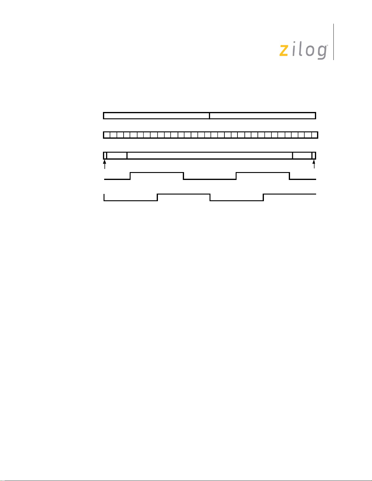
ISCC
Ignored
No Change No Change
Bit Cell
Count
Correction
RX DPLL Out
+1 -1
TX DPLL Out
118 19 201716 21 22 23 24 25 26 27 28 29 30 31 2 3 4 5 7 8 9 12 13 141110 150
6
Page 37 of 316
User Manual
counter dependent upon which region the transition on the receive data input occurred.
This is shown in Figure 3-7.
37
Figure 3–10. DPLL Operation in the FM Mode
In FM mode, the transmit clock and re ceive clock outputs from the DPLL are not in phase.
This is necessary to make the transmit and receive bit cell boundaries coincide, since the
receive clock must sample the data one-fourth and three-fourths of the way through the bit
cell.
Ordinarily, a bit cell boundary will occur between count 15 or count 16, and the DPLL
receive output will cause the data to be sampled at one-fourth and
three-fourths of the way
through the bit cell.
However, four variations may happen:
4. The DPLL actually allows the transition marking a bit-cell boundary to occur any-
where during the second ha
lf of count 15 or the first half of count 16, without making
a correction to its count cycle.
5. If t
he transition marking a bit cell boundary occurs
between the middle of count 16
and the middle of count 19, the DPLL is sampling the data too early in the bit cel
l. In
response to this, the DPLL extends its count by 1 during the next 0 to 31 counting
cycle, which effectively moves the receive clock edges closer to where they should be.
Any transitions occurring between the middle of count 19 in one cycle and the middle of
count 12
during the next cycle are ignored by the DPLL. This is necessary to guarantee
that any data transitions in the bit cells will not cause an adjustment to the counting cycle.
6. If no transition occurs between the middle of count 12 and the middle of count 19, the
DPLL is probably not locked onto the data properly. When the DPLL
the One Clock Missing bit is RR10, it is set to “1” and latched. It will hold this value
until a Reset missing Clock command is issued in WR14 or until the DPLL is disabled
UM011002-0808
misses an edge,
Page 44

ISCC
Page 38 of 316
User Manual
or programmed to enter the Search mode. Upon missing this one edge, the DPLL
takes no other action and does not modify its count during the next counting cycle.
7. If the DPLL does not see an edge between the middle of count 12 and the middle of
count 19 in two successive 0 to 31 count cycles, a line error condition is assumed. If
this occurs, the T wo Clocks Missing bit in RR10 is set to “1” and latched. At the same
time, the DPLL enters the Search mode. The DPLL makes the decision to enter Search
mode during count 2, where both the receive clock and transmit clock outputs are
LOW. This prevents any glitches on the clock outputs when search mode is entered.
While in search mode, no clock outputs are provided by the DPLL. The Two Clocks
Missing bit in RR10 is latched until a Reset Missing Clock command is issued in
WR14, or until the DPLL is disabled or programmed to enter the Search mode.
38
While the DPLL is disabled, the transmit clock
output of
the DPLL may be toggled by
alternately selecting FM and NRZI move in the DPLL. The same is true of the receive
clock.
While the DPLL is in Search mode, the counte
r remains at count 16, where the receive
output is LOW and the transmit output is LOW. This fact can be used to provide a transmit
clock under software control since the DPLL is in Search mode while it is disabled.
As in NRZI mode, if an adjustment to the counting cycle is nec
essary , the DPLL modifies
count 5, either deleting it or doubling it. If no adjustment is necessary, the count sequence
proceeds normally.
From the above discussion, together with an examination of
FM0 and FM1 data encoding,
it should be obvious that only clock transitions should exist on the receive data pin when
the DPLL is programmed to enter search mode. If this is not the case, the DPLL may
attempt to lock on to the data transitions.
With FM0 encoding this requires continuous “1s” received when leaving Search. In FM1
encoding, it is continuo
us “0s”; with Manchester encoded data this means alternating “1s”
and “0s.” With all three of these data encoding methods there will always be at least one
transition in every bit cell, and in FM mode the DPLL is designed to expect this transition.
3.5.3 DPLL Operation and Encoding in the Manchester Mode
UM011002-0808
The ISCC can encode Manchester data using the external logic shown in Figure 3-8, and it
can decode Manchester data using the DPLL. Recall that Manchester encoded data contains a transition at the center of every bit cell; it is the direction of this transition that distingu
ishes a “1” from a “0.” Hence, for Manchester data, the DPLL should be in FM
but the receiver should be set up to accept NRZ data. As with the FM modes, when
mode,
in the Search Mode the data stream should contain only clock transitions.
Page 45

ISCC
Transmit Clock
1
2
3
4
5
NRZ
ab
Manchester
NRZ
Transmit Clock
1
2
3
4
5
Page 39 of 316
User Manual
39
UM011002-0808
Figure 3–11. Encoding Manchester Data
Page 46

3.6 CLOCK SELECTION
Page 40 of 316
The ISCC can select several clock sources for internal and external use. Write Register 11
is the Clock Mode Control register for both the receive and transmit clocks. It determines
the type of signal on the /SYNC and /RTxC pins and the direction of the /TRxC pin.
ISCC
User Manual
40
The ISCC may be programmed to select one of severa
receive clocks.
The source of the receive clock is controlled by bits D6 and D5 of WR11. The receive
clock may be programmed to come from th
baud rate generator, or the receive output of the DPLL.
The source of the transmit clock is controlled by bits D4 and D3 of WR1
clock may be programmed to come from the /RTxC pin, the /TRxC pin, the output of the
baud rate generator, or the transmit output of the DPLL.
Ordinarily the /TRxC pin is an input, but it becomes an output if this pin has not been
selected as the source for the
The selection of the signal provided on the /TRxC output pin is controlled by bits D1 and
D0 of WR11. The /TRxC pin may be programmed to provide the output of the crystal
oscillator, the output of the baud rate generator, the receive output of the DPLL or the
actual transmit clock. If the output of the crystal oscillator is selected, but the crystal oscillator has not been enabled, the /TRxC pin will be driven HIGH. The option of placing the
transmit clock signal on
output of the DPLL.
Figure 3-9 shows a simplified schematic diagram of the circuitry used in the clock multiplexing. It shows the inputs to the multiplexer section, as well as the
sions that occu
r in the paths to the outputs.
transmitter or the receiver, and bit D2 of WR11 is set to “1.”
the /TRxC pin when it is an output allows access to the transmit
e /RTxC pin, the /TRxC pin, the output of the
l sources to provide the rece
1. The transmit
various signal inver-
ive and
UM011002-0808
Page 47

ISCC
OSC
/SYNC
/RTxC
OSC
Receiver
RX
TX
DPL
L
BRG
/TRxC
Baud Rate
Generator Out
Tx DPLL Out
Rx DPLL Out
PCL
K
Echo
Baud Rate
Generator
DPPL
Transmitter
Echo
Page 41 of 316
User Manual
41
UM011002-0808
Figure 3–12. Clock Multiplexer
Selection of the clocking options may be done anywhere in the initialization sequence, but
the final values must be selected before the receiver, transmitter, baud rate generator, or
DPLL are enabled to prevent problems from arbitrarily narrow clock signals out of the
multiplexers. The same is true of the crystal oscillator, in that the output should be allowed
to stabilize before it is used as a clock source.
Also shown are the edges used by the receiver, transmitter, baud
rate generator and DPLL
to sample or send data or otherwise change state. For example, the receiver samples data
on the falling edge, but since there is an inversion in the clock path between the /R TxC pin
and the receiver, a rising edge of the /RTxC pin samples the data for the receiver.
Page 48

ISCC
SCC
B
R
G
16x
Output
TxC
RxC
/TRxC Pin
/RTxC Pin
/SYNC Pin
External
Crystal
010110
/TRxC Out = BRG Output
11
D7 D6 D5 D4 D3 D2 D1 D0
/TRxC Pin = Output Pin
Tx Clock = BRG Output
Rx Clock = BRG Output
Using External Crystal
0
BRG Clock Source = /RTxC or
XTAL Oscillator
D1
WR11
WR14
SCC
NRZ Data
RxD Pin
SYNC
Modem
/RTxC Pin
RxC
TxC
1x
Page 42 of 316
User Manual
42
Figure 3–13. Async Transmission, 16x Clock Mode Using External Crystal
Figure 3–14. Async Transmission, 1x Clock Rate, NRZ Data Encoding
UM011002-0808
Page 49

ISCC
B
R
G
16x Data Rate
Txc
Rxc
/RTxC Pin
/SYNC Pin
External
Crystal
D
P
L
L
RxD Pin
RxD
Page 43 of 316
User Manual
43
Figure 3–15. Asynchronous Transmission, 1x Clock Rate, FM Data Encoding
Fig 3-10 shows the clock set up for asynchronous transmission, 16x clock mode using the
on chip oscillator with an external crystal. The registers involved are WR11 and WR14
and the figure shows the programming in these registers. Figure 3-11 shows asynchronous
communication where a 1x clock is obtained from an external MODEM. The data encoding is NRZ.
Note: that the BRG is not used un
The
x1 mode in Asynchronous mode is a combination of both synchronous and asynchronous transmission. The data are clocked by a common timing base, but characters are still
framed with S
detecting the first High-to-Low transition before beginning to assemble characters, the
data and clock must be synchronized externally. The x1 mode is the only mode in which a
data encoding method other than NRZ may be used.
Figure 3-12 shows the use of the DPLL to derive a 1x clock from the data. In this example:
•
•
tart and Stop bits. Because the receiver waits for one clock period after
The DPLL clock input = BRG output (x16 the data rate) WR14.
The DPLL clock output = RxC (receiver clock) WR11.
der this configuration.
UM011002-0808
Page 50

•
Page 44 of 316
Set FM mode WR14.
•
Set FM mode WR10.
3.7 CRYSTAL OSCILLATORS
For a given channel, if bit D7 of WR11 is set to 1, the crystal oscillator is enabled and a
high-gain amplifier is connected between the /RTxC pin and the /SYNC pin. While the
crystal oscillator is enabled, anything that has selected /RTxC as its clock source will automatically be connected to the output of the crystal oscillator. This also makes the /S
pin unavailable for other use.
In synchronous modes, no sync pulse is output, and the External Sync mode cannot be
selected. In asynchronous modes, the st
trolled by the /SYNC pin. Instead, the Sync/Hunt bit is forced to “0.” The crystal oscillator
requires some finite time to stabilize and must be allowed to stabilize before it is used as a
clock source. The External C
rystal used should operate in parallel resonance.
ISCC
User Manual
44
YNC
ate of the Sync/Hunt bit in RR0 is no longer con-
UM011002-0808
Page 51

ISCC
Page 45 of 316
User Manual
Chapter 4 Dat a Communication Modes
4.1 INTRODUCTION
The ISCC™ provides two independent full-duplex channels programmable for use in any
common asynchronous or synchronous data comm unication protocols. The data communication protocols handled by the SCC cell within the ISCC are:
•
Asynchronous Mode
•
Character-Oriented Mode
•
Monosynchronous
•
Bisynchronous
45
•
External Synchronous
•
Bit-Oriented Mode
•
SDLC
•
SDLC Loop Mode
4.1.1 General Description of the Transmitter
A block diagram of the transmitter is given in Figure 4-1. The transmitter has an 8-bit
Transmit Data register (WR8) loaded from the internal data bus and a Transmit Shift register loaded from either WR6, WR7, or the Transmit Data register . In byte-oriented modes,
WR6 and WR7 can be programmed with sync characters
6-bit sync character is used (WR6), whereas a 16-bit sync character is used (WR6 and
WR7) in Bisync mode. In bit-oriented synchronous modes, the flag contained in WR7 is
loaded into the Transmit Shift register at the beginning and end of a message.
. In Monosync mode, an 8-bit or
UM011002-0808
Page 52

ISCC
RxD Delayed
One Bit
WR7 Sync
Register
WR6 Sync
Register
WR5 Transmit
Data
Final Tx
MUX
NRZI
Encode
RxD
Internal
TxD
To Other
Channel
Internal Data Bus
20-Bit
Transmit
Shift
Register
Start
Bit
SYNC
ASYNC
SDLC
CRC SDLC
CRC
Generator
Zero Insert
(5-Bits)
Transmit
MUX &
2-Bit Delay
TxD
Transmit
Clock
Page 46 of 316
User Manual
46
UM011002-0808
Figure 4–16. Transmitter Block Diagram
If asynchronous data is processed, WR6 and WR7 are not used and the Transmit Shift register is formatted with start and stop bits shifted out to the transmit multiplexer at the
selected clock rate. Synchronous data (except SDLC/HDLC
) is shifted to the CRC genera-
tor as well as to the transmit multiplexer.
SDLC/HDLC
(which
is disabled while the flags are being sent). A “0” is inserted in all address, control,
information, and frame check fields following five contiguous “1s” in the data stream. The
result of the CRC generator for SDLC data is also routed through the zero insertion logic
data is shifted to the CRC Generator and out through the zero insertion logic
and then to the transmit multiplexer.
Page 53
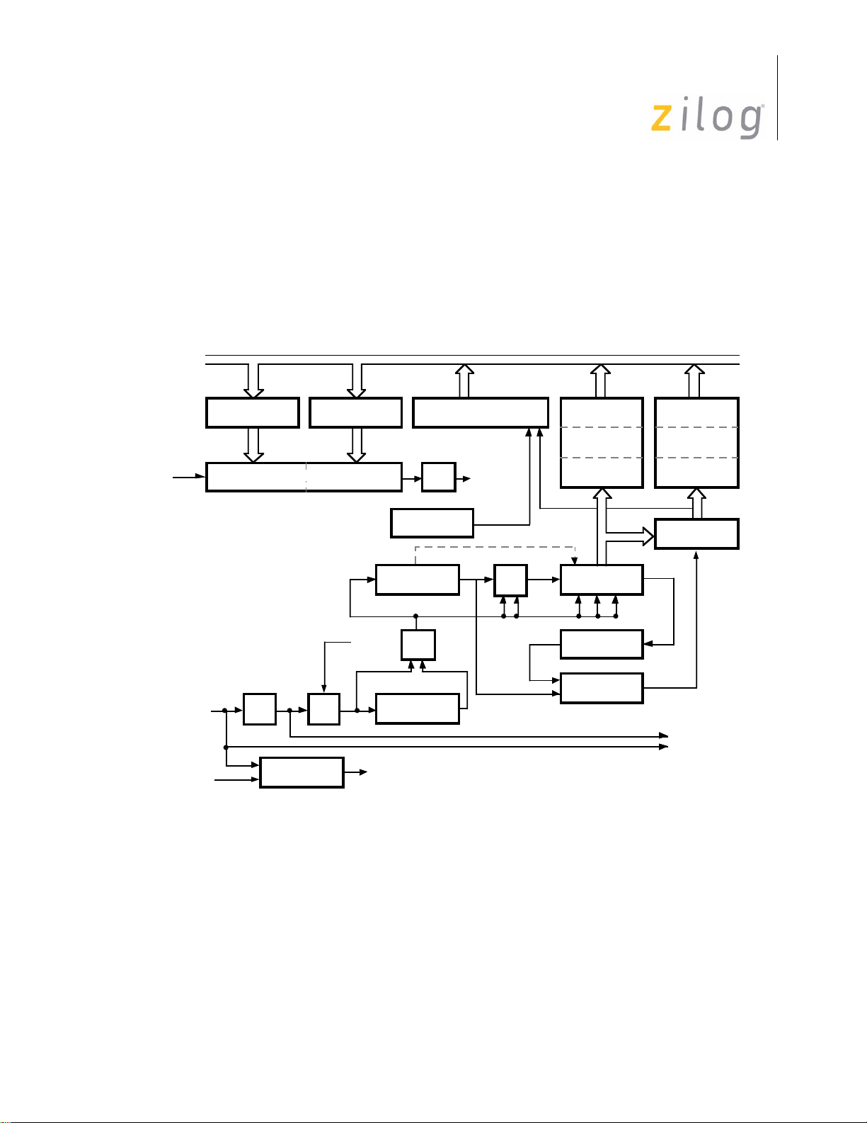
4.1.2 General Description of the Receiver
WR13 Upper Byte
Time Constant
DPLL
WR12 Lower Byte
Time Constant
10 X 19 Frame
Status FIFO
Internal Data Bus
Receive
Data
FIFO
Receive
Error
FIFO
÷ 2
14-Bit Counter
16-Bit Down Counter
BR
Generator
Output
Receive
Error Logic
Receive Sync
Register (8-Bits)
CRC Delay
Register (8-Bits)
CRC
Checker
3 Bits
Sync Register
& Zero Delete
MUX
Sync
CRC
1-Bit
NRZI Decode
Internal
TxD
DPLL
DPLL Output
MUX
To Transmitter
CRC Result
SDLC CRC
Hunt Mode (Bisync)
BR
Generator
Input
RxD
Page 47 of 316
The receiver has a three deep, 8-bit Data FIFO (paired with a three deep Error FIFO), and
an 8-bit shift register. The receiver block diagram is shown in Figure 4-2. This arrangement creates a three-character delay time, which allows the CPU time to service an interrupt at th
Error FIFO stores parity and framing errors and other types of status information. The
Error FIFO is
e beginning of a block of high-speed data. With each Receive Data FIFO, the
readable in Read Register 1.
ISCC
User Manual
47
UM011002-0808
Incoming data is routed through one of several paths depending on the mode and character
length. In Asynchronous mode, serial data enters the 3-bit delay if the character length of
seven or eight bits is selected. If a character length of five or six bits is selected, data enters
the receive shift register directly.
In synchronous modes, the data path is determined by the phase of the rec
rently in operation. A synchronous receive operation begins with a hunt phase in which a
bit pattern that matches the programmed sync characters (6-,8-, or 16-bit is searched).
Figure 4–17. Receiver Block Diagram
eive process cur-
Page 54

ISCC
Page 48 of 316
User Manual
The incoming data then passes through the Sync register and is compared to a sync character stored in WR6 or WR7 (depending on which mode it is in). The Monosync mode
matches the sync character programmed
in WR7 and the character assembled in the
Receive Sync register to establish synchronization.
48
Synchronization is achieved differently in the Bisync mode. Incoming
data is shifted to the
Receive Shift register while the next eight bits of the message are assembled in the
Receive Sync register. If these two characters match the programmed characters in WR6
and WR7, synchronization is established. Incoming data can then bypass the Receive Sync
register and enter the 3-bit delay directly.
The SDLC mode of operation uses the receive Sync register to monitor the receive
data
stream and to perform zero deletion when necessary; i.e., when five continuous “1s” are
received, the sixth bit is inspected and deleted from the data stream if it is “0”. The seventh
bit is inspected only if the sixth bit equals one. If the seventh bit is “0”, a flag sequence has
been received and the receiver is synchronized to that flag. If the seventh bit is a “1” an
abort or an EOP (End Of Poll) is recognized, depending upon the selection of either the
normal SDLC mode or SDLC Loop mode.
The same path is taken by incoming data for both SDLC modes. The reformatted data
enters the 3-bit delay an
d is transferred to the Receive Shift register. The SDLC receive
operation begins in the hunt phase by attempting to match the assembled character in the
Receive Shift Register with the flag pattern in WR7. Then the flag character is recognized,
subsequent data is routed through the same path, regardless of character length.
Either the CRC-16 or CRC-SDLC cyclic redundancy
us
ed for both Monosync and Bi-sync modes, but only the CRC-SDLC polynomial is used
check (CRC) polynomial can be
for SDLC operation. The data path taken for each mode is als o different. Bisync protocol
is a byte-oriented operation that requires the CPU to decide whether or not a data character
is to be included in CRC calculation. An 8-bit delay in all synchronous modes except
SDLC is allowed for this process. In SDLC mode, all bytes are included in the CRC calculation.
UM011002-0808
Page 55

4.2 ASYNCHRONOUS MODE
Idle State
of Line
LSB
1
0
Start
Bit
Parity
Bit
Data Field
Stop
Bit(s)
1.5
1
2
Page 49 of 316
In asynchronous communications data is transferred in the format shown in Figure 4-3.
Figure 4–18. Asynchronous Message Format
ISCC
User Manual
49
The transmission of a character begins when the line makes a transition from the “1”
state, or MARK condition to the “0” state or SPACE condition. This transition is the reference by which the character’s bit cell boundaries are defined. Though the transmitter an
d
receiver have no common clock signal, there must be an agreement as to the data rate so
that the receiver can always sample the data in the center of the bit cell.
The character can be broken up into four fields:
8. Start bit - signals the beginning of a character frame.
9. Data field - typi
cally 5-8 bits wide.
10. Parity bit - optional, provides mechanism for checking character validity, transmitter
and receiver agree that:
11. Data + Parity bit contains odd number of 1s (odd parity) or Data + Parity bit contains
even number of 1s (even parity).
Stop bit(s) - provides a minimum interval betwee
n the end of one chara
cter and the begin-
ning of the next.
The ISCC™ supports Asynchronous mode with a number of programmable options
including the number of bits per character, the nu
mber of stop bits, the clock factor,
modem interface signals and break detect and generation.
Asynchronous mode is selected by programming the desired number of stop bits in D3 and
D2 or WR4. Programming these two bits with other th
an “00” places both the receiver and
transmitter in Asynchronous mode. In this mode, the ISCC ignores the state of bits D4,
D3, and D2 of WR3, bits D5 and D4 of WR4, bits D2 and D0 of WR5, all of WR6 and
UM011002-0808
Page 56

User Manual
Page 50 of 316
WR7 and all of WR10 except D6 and D5. Bits that are ignored may be programmed with
“1” or “0” or not at all. See Table 4-1 below
Table 4–9. Write Register Bits Ignored in Asynchronous Mode
Register D7 D6 D5 D4 D3 D2 D1 D0
WR3 x x x
WR4 x x
WR5 x x
WR6 x x x x x x x x
WR7 x x x x x x x x
WR10 x x x x x x
ISCC
50
4.2.1 Asynchronous Transmit
Characters are loaded from the transmit buffer to the shift register where they are given a
start bit and a parity bit (if programmed), and are shifted out to the TxD pin. Each time the
transmit buffer becomes empty the Tx Empty bit in RR0 is set to 1 and, optionally, an
interrupt or DMA request can be generated.
The number of bits transmitted per character is controlled both by Bits D6 and D5 in
WR5, and the way the data is formatted
the option of five, six, seven, or eight bits per character. When five bits per character is
selected the data may be formatted before being written to the transmit buffer to allow
transmission of from one to five bits per character.
This formatting is shown in Table 4-2.
Table 4–10. Transmit Bits per Character
Bit 7 Bit 6
0 0 5 or less bits/character
0 1 7 bits/character
1 0 6 bits/character
1 1 8 bits/character
within the transmit buffer . The bi ts in WR5 allow
UM011002-0808
Page 57
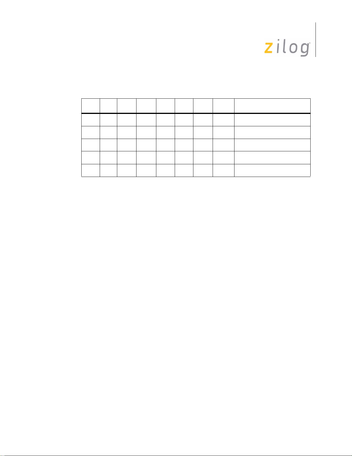
ISCC
Page 51 of 316
User Manual
For five or less bits per character selection in WR5, the following encoding is used in the
data sent to the transmitter. D is the data bit(s) to be sent.
D7 D6 D5 D4 D3 D2 D1 D0
1 1 1 1 0 0 0 D Sends one data bit
1 1 1 0 0 0 D D Sends two data bits
1 1 0 0 0 D D D Sends three data bits
1 0 0 0 D D D D Sends four data bits
0 0 0 D D D D D Sends five data bits
In all cases the data must be right-justified, with the unused bits being ignored except in
the case of five bits or less per character.
51
An additional bit, carrying parity information, may be automatically appended to every
transmitted character by setting
number of bits specified in WR4 or by the data format. The parity sense is selected by bit
D1 of WR4. If this bit is set to “1”, the transmitter sends even parity, if set to “0”, the parity is odd.
The ISCC may be programmed to accept a transmit clock that is one, sixteen, thirty-two,
or sixty-four times the data rate. This is
with the clock factor for the receiver. Note that the chosen clock factor may restrict the
number of stop bits that may be transmitted. In particular, when the clock rate and data
rate are identical, one-and-a-half stop bits are not allowed. If any length other than one
stop bit is desired in the times one mode, only two stop bits may be used.
There are two modem control signals associated with the transmitter provided by the
ISCC, namely /R TS and /CTS.
The /R
TS pin is a simple output that carries the inverted state of the RTS bi
unless the Auto Enables bit (D5) is set in WR3. When Auto Enables is set, the /RTS pin
will immediately go Low when the RTS bit is set. However, when the RTS bit is reset, the
/RTS pin remains Low until the transmitter is completely empty and the last stop bit has
left the TxD pin. Thus the /RTS pin may be used to disable external drivers for the transmit data.
The /CTS pin is ordinarily a simple input to the CTS
mode is selected this pin becomes an enable for the transmitter. That is, if Auto Enables is
on and the /CTS pin is High, the transmitter is disabled; the transmitter is enabled while
the /CTS pin is Low.
bit D0 of WR4 to “1”. This bit is sent in addition to the
selected by bits D7 and D6 of WR4, in common
t (D1) in WR5,
bit in RR0. However, if
Auto Enables
UM011002-0808
The transmitter may be programmed to send a Break by setting bit D4 of WR5 to “1”.
transmitter will send continuous “0s” from the first transmit clock edge after this com-
The
Page 58

ISCC
Page 52 of 316
User Manual
mand is issued, until the first transmit clock edge after this bit is reset. The transmit clock
edges referred to here are those that define transmitted bit cell boundaries.
An additional status bit for use in Asynchronous mode is available in bit D0 or RR1. This
bit, called All Sent, is set when the transmitter is completely empty and any previous data
or stop bits have reached the TxD pin. The All Sent bit can be used by the processor as an
indication that the transmitter may be safely disabled.
The initialization sequence for the transmitter in asynchro-nous mode is given in
Table 4-3.
52
At this point other
clocking, I/O mode, etc. When all t
ting WR5(3) = 1. Also note that the transmitter and receiver may be initialized at the same
time.
The num
Table 4–11. Initialization Sequence for the Transmitter in Asynchronous Mode
ber of bits/char is selected by WR3, bits 6-7.
registers should be initialized according to the hardware design such as
his is completed, the transmitter may be enabled by set-
Reg Bit No Description
WR4 3, 2 Select Async Mode and the number of stop bits*
0, 1 Select parity*
6, 7 Select clock mode*
WR3 5 Select Auto Enable Mode*
WR5 1 Select modem control (RTS)
4 Select break generation
6, 5 Select number of bits/char for transmitter
Note: * Initializes transmitter and receiver simultaneously
4.2.2 Asynchronous Reception
UM011002-0808
During reception, the start and stop bits are stripped away and checked for errors, leaving
only the working data for CPU interaction.
The receiver always checks for one stop bit. If after ch
this stop bit to be a “0”, the Framing Error bit in the receive error FIFO is set at the same
time that the character is transferred to the receive data FIFO. This error bit accompanies
the data to the top of the FIFO, where it generates a special receive condition. The Framing Error bit is not latched, and so must be read in RR1 before the accompanying data is
read.
aracter assembly the receiver finds
Page 59

ISCC
Page 53 of 316
User Manual
The additional parity bit per character is transferred to the receive data FIFO along with
the data if the data plus parity is eight bits or less. The Parity Error bit in the receive error
FIFO may be programmed to cause a special receive condition interrupt by setting bit D2
of WR1 to “1”. This error bit is latched and so will remain active, once set, until an Error
Reset command has been issued. If interrupts are not used to transfer data, the Parity Error,
Framing Error, and Overrun Error bits in RR1 should be checked before the data is
removed from the receive data FIFO.
The ISCC™ may be programmed to accept a receive clock that is one, sixteen, thirty-two,
or sixty-four times the data rate. This is selected by bits D7 and D6 in WR4. The 1X mod e
is used when bits are synchronized external to the receiver. The 1X mode is the only mode
in which a data encoding method other than NRZ may be used. The clock factor is common to the receiver and transmitter.
53
The ISCC provides up to three modem control signals associated
with the receiver.
The /SYNC pin is a general-purpose input whose state is reported in the Sync/Hunt bit in
RR0. If the crystal osci
llator is enabled, this pin is not available and the Sync/Hunt bit is
forced to “0”. Otherwise, the /SYNC pin may be used to carry the Ring Indicator signal.
The /DTR//REQ pin carries the inverted state of the DTR bit (D7) in WR5 unless this pin
has been programmed to carry a DMA Reque
The /DCD pin is ordinarily a simple input to the DCD bit in RR0. However
Enables mo
de is selected by setting D5 of WR3 to “1”, this pin becomes an enable for the
st signal.
, if the Auto
receiver. That is, if Auto Enables is on and the /DCD pin is High, the receiver is disabled.
While the /DCD pin is Low, the receiver is enabled.
The break condition is continuous “0s”, as opposed to the usual continuous ones during an
idle. The ISCC recognizes the Break condition upon seeing a null character (all “0s”) plus
a framing error. Upon
recognizing this sequence the Break bit in RR0 will be set and will
remain set until a “1” is received. At this point the break condition is no longer present. At
the termination of a break the receive data FIFO contains a single null character, which
should be read and discarded. The Framing Error bit will not be set for this character, but
if odd parity has been selected, the Parity Error bit will be set. Caution should be exercised
if the receive data line contains a switch that is not debounced to generate breaks. Switch
bounce may cause multiple breaks, recognized by the ISCC to be additional characters
assembled in the receive data FIFO. It may also cause a receive overrun condition being
latched.
UM011002-0808
Received characters are assembled, checked for errors, and moved to a three byte FIFO
.
When there is at least one character in the FIFO the Rx Character A vailable bit (in RR0) is
set to 1 and, optionally, an interrupt or DMA request can be generated. Since errors apply
to specific characters, it is necessary that error information moves along side the data that
it refers to. This is implemented in the ISCC with a three entry error FIFO in parallel with
Page 60

ISCC
Page 54 of 316
User Manual
the data FIFO. The three error conditions that the receiver checks for in asynchronous
mode are:
1. Framing errors - when a character stop bit is found to be 0.
2. Parity errors - when parity is enabled and the parity of a character disagrees with the
sense programmed in WR4.
3. Overrun errors - when the FIFO overflows.
The initialization sequence for the receiver in asynchronous mode is given in Table 4-4
below.
Table 4-4. Initialization Sequence for the Receiver in Asynchronous Mode
Table 4–12. Initialization Sequences for the Receiver in Asynchronous Mode
Reg Bit No Description
54
WR4 3, 2 Select Async Mode and the number of stop bits*
0, 1 Select parity*
6, 7 Select clock mode*
WR3 7, 6 Select number of bits/character
5 Select Auto Enable Mode*
WR5 1 Select modem control (RTS)
Note: * Initializes transmitter and receiver simultaneously
At this point other registers should be initi
clocking,
ting WR3(0) = 1. Also note that the transmitter and receiver may be initialized at the same
time.
I/O mode, etc. When all this is completed, the receiver may be enabled by set-
alized according to the hardware design such as
4.3 BYTE-ORIENTED SYNCHRONOUS MODE
Three byte-oriented synchronous protocols supported by ISCC are monosync, bisync, and
external sync.
UM011002-0808
In synchronous communications the bit cell b
which is common to both the transmitter and receiver. Of course there must also be an
agreement as to the location of the character boundaries so that the characters can be properly framed. This is normally accomplished by
characters. The SYNC pattern serves as a reference; it signals the receiver that a character
boundary occurs immediately after the last bit of the pattern. Another way of identifying
oundaries are defined by
defining special SYNC patterns, or SYNC
a clock signal
Page 61

ISCC
Modem Clock
Bit
Bit State
Data
LSB
Sync Character Data Character
1 Bit Time
1 2 3 4 5 6 7 8 9 10 11 12 13 . . .
0 1 1 0 1 0 0 0 1 1 0 1 0 1 0 1
Page 55 of 316
User Manual
the character boundaries (i.e., achieving synchronization) is with a logic signal that goes
active just as the first character is about to enter the receiver. This method is referred to as
“External Synchronization”.
Figure 4-4 shows the character format for synchronous transmission. For example, bits 18 might be one character and bits 9-13 part of another character; or bit 1 might be part of a
second character, and bits 10-13 part of a third character. The alignment of the received
bytes to the byte assembly is accomplished by defining a synchronization character, commonly called a “sync character”.
55
Figure 4–19. Monosync Data Character Format
Start and stop bits are not required in synchronous modes. All bits are used to transmit
data. This eliminates the “waste” characteristic of asynchronous communication.
4.3.1 Byte Oriented Synchronous Transmit
Once Synchronous mode has been selected, any of three sync character lengths may be
selected:
6-bit
8-bit
16-bit
The 6-bit option Sync character is selected by setting bits 4 and 5 of WR4 to zeros and bit
0 of WR10 to one. Only the least significant
The 8-bit sync character is selected by setting bits 4 and 5 of WR4 to zeros and bit 0 of
WR10 to zero. With
it has no data to send.
Monosync and Bisync modes require clocking information to be transmitted along with
th
e data either by a method of encoding data that contains clocking information, or by a
this option selected, the transmitter sends the contents of WR6 when
six bits of WR6 are transmitted.
UM011002-0808
Page 62

ISCC
Page 56 of 316
User Manual
modem that encodes or decodes clock information in the modulation process. Refer to the
Monosync message format as shown in Figure 4-4.
The Bisync mode of operation is similar to the Monosync mode, except that two sync
characters are provided instead of one. Bisync attempts a more structured approach to synchronization through the use of special characters as message “headers”
or “trailers”.
56
External Sync mode eliminates the use of sync characters in the
viding an external sync signal to mark the beginning of a data field; i.e., an external input
pin (Sync) waits for an active state c
field.
Character-oriented mode is selected by programming bits D3 and D2 of WR4 with zeros.
This selects synchronous mode
further modified by bits 5 to 7 of WR4 as well as bits 1 and 0 of WR10. In sync character oriented modes, except External Sync mode, the state of bits 7 and 6 of WR4 are always
forced internally to zeros. In external sync mode, these two bits must be programmed as
described in Section 5.4.5.
Table 4–13. Registers Used in Character-oriented Modes
hange to indicate the beginning of an information
, as opposed to asynchronous mode, but this selection is
serial data stream by pro-
Register Bit No Description
WR4 3 (=0) Select sync mode
2 (=0)
4 (=0) Select monosync mode
5 (=0) (8-bit sync character)
4 (=1) Select bisync mode
5 (=0) (16-bit sync character)
4 (=1) Select external sync mode
5 (=1) (external sync signal required)
6 (=0) Select 1x clock mode
7 (=0)
WR6 7-0 Sync character (low byte)
WR7 7-0 Sync character (high byte)
WR10 1 Select sync character length
UM011002-0808
Page 63

ISCC
Page 57 of 316
User Manual
In character-orie nted m ode s, a special bit pattern is used to provide character synchronization. The ISCC offers several options to support synchro nous mode including various sync
generation and che
cking, CRC generation and checking, as well as modem controls and a
transmitter to receiver synchronization function.
For a 16-bit sync character, set bit D4 of WR4 to “1” and bit D5 of WR4 and bit D0 of
WR10 to “0”. In this mode the transmitter sends the concatenation
of WR6 and WR7 as a
time fill.
Because the receiver requires that sync characters be left-justified in the registers, while
the transmitter requires them to be right justified, only the recei
ver will work with a 12-bit
sync character. While the receiver is in External Sync mode, the transmitter sync length
may be six or eight bits, as selected by bit D0 of WR10.
The number of bits per transmitted character is controlled by D6 and D5 of WR5 and the
way the data is formatted within th
e transmit buffer. The bits in WR5 allow the option of
five, six, seven, or eight bits per character. When five bits per character is selected the data
may be formatted before being written to the transmit buffer to allow transmission of from
one to five bits per character. This formatting is shown in Table 4-2. In all cases the data
must be right-justified, with the unused bits being ignored except in the case of five bits
per character.
57
An additional bit, carrying parity
transmitted character by setting bit
information, may be automatically appended to every
D0 of WR4 to “1”. This parity bit is sent in addition to
the number of bits specified in WR4 or by the data format. If this bit is set to “1”, the
transmitter will send even parity, if set to “0”, the transmitted parity will be odd.
Either of two CRC polynomials may be used in synchronous modes, selected by bit D2 in
WR5. If this bit is set to “1”, the CRC-16 polynomial is used and, if this bit is set to “0”,
the CRC-CCITT polynomial is used.
This bit controls the selection for both the transmitter
and receiver. The initial state of the generator and checker is controlled by bit D7 of
WR10. When this bit is set to “1”, both the generator and checker will have an initial value
of all ones, if this bit is set to “0”, the initial values will be all zeros.
The ISCC does not automatically preset the CRC generator, so this must
be done in software. This is accomplished by issuing the Reset Tx CRC Generator command, which is
encoded in bits D7
and D6 of WR0. For proper results this command must be issued while
the transmitter is enabled and sending sync characters.
If CRC is to be used, the transmit CRC generator must be enabled by setting bit D0 of
WR5 to “1”
. This bit may also be used to exclude certain characters from the CRC calculation. Sync characters are automatically excluded from the CRC calculation and any
characters written as data
may also be excluded from the calculation by using bit D0 of
WR5. Internally , the CRC is enabled or disabled for a particular character at the same time
as the character is loaded from the transmit buffer to the Transmit Shift register. Thus, to
exclude a character from CRC calculation bit D0 of WR5 should be set to “0” before the
character is written to the transmit buffer. This guarantees that the internal disable will
UM011002-0808
Page 64

ISCC
Page 58 of 316
User Manual
occur when the character moves from the buffer to the shift register. Once the buffer
becomes empty, the Tx CRC Enable bit may be written for the next character.
Enabling the CRC generator is not sufficient to control the transmission of CRC. In the
ISCC this function is controlled by the Tx Underrun/EOM bit, which may be reset by the
processor and set by the ISCC. When the transmitter underruns (both the transmit buffer
and Transmit Shift register are empty) the state of the Tx Underrun/EOM bit determines
the action taken by the ISCC. If the Tx Underrun/EOM bit is not set when the underrun
occurs, the transmitter will send the accumulated CRC and set the Tx Underrun/EOM bit
to indicate this. This transition may be programmed to cause an external/status interrupt,
or the Tx Underrun/EOM is available in RR0.
The Reset Tx Underrun/EOM Latch command is encoded in bits D7 and D6 of WR0. For
correct transmission of the CRC at the end of a block
issued after the first character is written to the ISCC but before the transmitter underruns
after the last character written to the ISCC. The command is usually issued immediately
after the first character is written to the ISCC so that CRC will be sent if an underrun
occurs inadvertently during the block of data.
of data, this command must be
58
If the transmitter is disabled during transmission of a character, that character will be sent
completely
disabled during the transmission of CRC, the 16-bit transmission will be completed, but
the remaining bits will come from the SYNC registers rather than the remainder of the
CRC.
There are two modem control signals associated with
ISCC: /RTS and /CTS.
The
The /CTS pin is ordinarily a simple input to the CTS bit in RR0. However , if
mode is selected this pin becomes an enable for the transmitter. That is, if Auto Enables is
ON and the /CTS pin is High the transmitter is disabled. While the /CTS pin is Low, transmitter is enabled.
The initialization sequence for the transmitter in character-oriented mode is shown in
Table 4-6.
Table 4–14. Transmitter Initialization in Character Oriented Mode
. This applies to both data and sync characters. However, if the transmitter is
the transmitter provided by the
/R TS pin is a simple output that carries the invert ed state of the RTS bi
t (D1) in WR5.
Auto Enables
Register Bit No Description
WR4 0,1 select parity
WR5 1 RTS
2 select CRC generator
UM011002-0808
Page 65

User Manual
Page 59 of 316
Table 4–14. Transmitter Initialization in Character Oriented Mode
Register Bit No Description
5,6 select number of bits
per character
WR10 7 CRC preset value
At this point, the other registers should be initialized as necessary . When all of this is completed the transmitter maybe enabled by setting bit 3 of WR5 to one. Now that the transmitter is enabled the CRC generator maybe initialized by issuing the Reset Tx CRC
Generator command in WR0, bit 6-7.
ISCC
59
4.3.2 Byte-Oriented Synchronous Receive
The CPU places the receiver in Hunt mode whenever transmission begins (or whenever a
data dropout has occurred and the hardware determines that resynchronization is necessary). In Hunt mode, the receiver shifts a bit into the Receive Shift register and compares
contents of the Receive Shift register and with the sync character (stored in another
the
register), repeating the process until a match occurs. When a match occurs, the receiver
begins transferring bytes to the receive FIFO.
Once the sync character-oriented mode has been selected, any of the four sync character
length maybe selected: 6-bits, 8-bits, 12-bits, or 16-bits.
Table 4-7 show s the WR register bit setting for selecting sync character le
The
Table 4-7. Sync Character Length Selection
Table 4–15. Sync Character Length Selection
Sync Length WR4,D5 WR4,D4 WR10,D0
6 bits 0 0 1
8 bits 0 0 0
12 bits 0 1 1
ngth.
UM011002-0808
16 bits 0 1 0
The arrangement of the sync character in WR6 and WR7 is
shown in Figure 4-5.
Page 66

ISCC
D6D7 D5 D4 D3 D2 D1 D0
Sync7
Sync1
Sync7
Sync3
ADR7
ADR7
Sync6
Sync0
Sync6
Sync2
ADR6
ADR6
Sync5
Sync5
Sync5
Sync1
ADR5
ADR5
Sync4
Sync4
Sync4
Sync0
ADR4
ADR4
Sync3
Sync3
Sync3
1
ADR3
x
Sync2
Sync2
Sync2
1
ADR2
x
Sync1
Sync1
Sync1
1
ADR1
x
Sync0
Sync0
Sync0
1
ADR0
x
Monosync, 8 Bits
Monosync, 6 Bits
Bisync, 16 Bits
Bisync, 12 Bits
SDLC
SDLC (Address Range)
Write Register 6
D6D7 D5 D4 D3 D2 D1 D0
Sync7
Sync5
Sync15
Sync11
0
Sync6
Sync4
Sync14
Sync10
1
Sync5
Sync3
Sync13
Sync9
1
Sync4
Sync2
Sync12
Sync8
1
Sync3
Sync1
Sync11
Sync7
1
Sync2
Sync0
Sync10
Sync6
1
Sync1
x
Sync9
Sync5
1
Sync0
x
Sync8
Sync4
0
Monosync, 8 Bits
Monosync, 6 Bits
Bisync, 16 Bits
Bisync, 12 Bits
SDLC
Write Register 7
Page 60 of 316
User Manual
60
UM011002-0808
Figure 4–20. sync Character Programming
For those applications requiring any other sync character length, the ISCC makes provision for an external circuit to provide a character synchr
onization signal on the /SYNC
pin. This mode is selected by setting bits D5 and D4 of WR4 to “1”. In this mode the
Sync/Hunt bit in RR0 reports the state of the /SYNC pin but the receiver must still be
placed in Hunt mode when the external logic is searching for a sync character match.
When the receiver is in Hunt mode and the /SYNC pin is driven Low, two receive clock
cycles after the last bit of the sync character is received, character assembly will begin on
the rising edge of the receive clock immediately preceding the activation of /SYNC.
Page 67

ISCC
/RTxC
RxD
/SYNC
SYN
C
SYN
C
DAT
A
0
DAT
A
1 DAT
A
2
Last- La
s
State changes in one
/RTxC clock cycle
/RTxC
PCLK
/SYNC
Page 61 of 316
User Manual
This is shown in Figure 4-6. The receiver leaves Hunt mode when /SYNC is driven Low.
Figure 4–21. /SYNC as an Input
In all cases except External Sync mode the /SYNC pin is an output that is driven low by
the ISCC to signal that a sync character has been received. The /SYNC pin is activated
regardless of character boundaries so any external circuitry using it should only respond
the /SYNC pulse that occurs while the receiver is in Hunt mode. The timing for the
/SYNC signal is shown in Figure 4-7.
61
UM011002-0808
Figure 4–22. /SYNC as an Output
It is sometimes desirable to prevent sync characters from entering the receive data FIFO.
This function is available in the ISCC by setting the Sync Character Load inhibit bit (D1)
in WR3 to “1”. While this bit is set to “1”, the character about to be loaded into the receive
data FIFO is compared with the contents of WR6. If all eight bits match the character, it is
not loaded into the receive data FIFO. Because the comparison is across eight bits, this
function works correctly only when the number of bits per character is the same as the
sync character length. Thus it cannot be used with 12- or 16-bit sync characters. Both leading sync characters and sync characters embedded in the data may be prop
erly removed in
the case of a 8-bit sync character. Care must be exercised in using this feature because
sync characters not transferred to the receive data FIFO will automatically be excluded
from CRC calculation. This works properly only in the 8-bit case.
Page 68

ISCC
Page 62 of 316
User Manual
The receiver in the ISCC searches for character synchronization only while it is in Hunt
mode. In this mode the receiver is idle having been first enabled, and may be placed in
Hunt mode by command from the processor. This is accomplished by issuing the Enter
Hunt Mode command in WR3. This bit (D4) is a command; writing a “0” to it has no
effect. The Hunt status of the receiver is reported by the Sync/Hunt is one of the possible
sources of external/status interrupts, with both transitions causing an interrupt. This is true
even if the Sync/Hunt bit is set as a result of the processor issuing the Enter Hunt Mode
command.
The number of bits per character is controlled by bits D7 and D6 of WR3. Five, six, seven,
or eight bits per character may be selected via these two bits. The data is right-justified in
the receive data buffer. The ISCC merely takes a snapshot of the receive data stream at the
appropriate times so the “unused” bits in the receive buffer are only the bits following the
character in the data stream.
An additional bit, carrying parity information, may be selected by setting bit D0 of WR4
to “1”. If this bit is set
to “1”, the received character is checked for even parity, if set to
“0”, the received character is checked for odd parity. The additional bit per character is not
visible when there are eight data bits per character. The Parity Error bit in the receive error
FIFO may be programmed to cause a Special Receive Condition interrupt by setting bit
D2 of WR1 to “1”. This error bit is latched and so will remain active, once set, until an
Error Reset command has been issued. If interrupts are not used to transfer data the Parity
Error, CRC Error, and Overrun Error bits in RR1 should be checked before the data is
removed from the receive data FIFO.
62
The character length may be changed at any time before the new number of bits has been
assembled by the receiver
, but, care should be exercised as unexpected results may occur.
A representative example, switching from five bits to eight bits and back to five bits is
shown in Figure 4-8.
UM011002-0808
Page 69

ISCC
654321
Receive Data Buffer
78
111098761213
19 18 17 16 15 142021
27 26 25 24 23 222829
32 31 30 29 28 273334
37 36 35 34 33 323839
Time
Change from Five to Eight
Change from Eight to Five
5 Bits
5 Bits
5 Bits
8 Bits
8 Bits
Page 63 of 316
User Manual
63
UM011002-0808
Figure 4–23. Changing Character Length
Either of two CRC polynomials may be used in synchronous modes, selected by bit D2 in
WR5. If this bit is set to “1”, the CRC-16 polynomial is used, if this bit is set to “0”, the
CRC-CCITT polynomial is used. This bit controls the polynomial selection for both the
receiver and transmitter.
The initial state of the generator and checker is controlled by bit D7 of WR10. When this
bit is set to “1”, both the generator and checker will have an initial value of all ones, if this
bit is set t
o “0”, the initial values will be all “0s”. The ISCC presets the checker whenever
the receiver is in Hunt mode so a CRC reset command is not strictly necessary. However,
there is a Reset CRC Checker command in WR0. This command is encoded in bits D7 and
D6 of WR0. If CRC is to be used the CRC checker must be enabled by setting bit D0 of
WR3 to “1”.
If sync characters are being stripped from the data stream, this may b
before the first non-sync character is received. If the sync strip feature is not being used,
CRC must not be enabled until after the first data character has been transferred to the
e done at any time
Page 70

ISCC
Page 64 of 316
User Manual
receive data FIFO. As previously mentioned, 8-bit sync characters stripped from the data
stream are automatically excluded from CRC calculation.
Some synchronous protocols require that certain characters be excluded from CRC calculation. This is possible in the ISCC because CRC calculation may be enabled and disabled
fly. To give the processor sufficient time to decide whether or not a particular char-
on the
acter should be included in the CRC calculation, the ISCC contains an 8-bit time delay
between the receive shift register and the CRC checker
. The logic also guarantees that the
calculation will only start or stop on a character boundary by delaying the enable or disable until the next character is loaded into the receive data FIFO.
derstand how this works refer to Figure 4-9 and the following explanation. Consider
T o un
a case where the ISCC re
ceives a sequence of eight bytes, called A, B, C, D, E, F , G and H
with A received first. Now suppose that A is the sync character, that CRC is to be calculated on B, C, E, and F , and that F is the last byte of this message. A process is use
d to con-
trol the ISCC as described below.
64
The Receive Character-Operational Stages:
1. Before A is received the receiver is in Hunt mode and
the CRC is disabled. When A is
in the receive shift register it is compared with the contents of WR7. Since A is the
sync character, the bit patterns match and receive leaves Hunt mode, but character A is
not transferred to the receive data FIFO.
2. After 8-bit times, B is loaded into the receive data FIFO. The CRC remains disabled
even though somewhere during the next eight bit times the processor reads B and
enables CRC. At the end of this eight-bit time, B is in the 8-bit delay and C is in the
receive shift register.
3. Character C is loaded into the receive data FIFO and at the same time the CRC
checker becomes enabled. During the next eight-bit-time, the processor reads C and
since CRC is enabled within this period, the ISCC has calculated CRC on character B;
character C is in the 8-bit delay and D is in the Receive Shift register. D is then loaded
into the receive data FIFO and at some point during the next eight-bit-time the processor reads D and disables CRC. At the end of these eight-bit-times CRC has been calculated on C, character D is in the 8-bit delay and E is in the Receive Shift register.
4. Now E is loaded into the receive data FIFO. During the next eight-bit-times the processor reads E and enables the CRC. During this time E shifts into the 8-bit delay, F
enters the Receive Shift register and CRC is not being calculated on D. After these
eight-bit-times have elapsed, E is in the 8-bit delay, and F is in the Receive Shift register. Now F is transferred to the receive data FIFO and CRC is enabled. During the next
eight-bit-times the processor reads F and leaves the CRC enabled. The processor is
usually aware that this is the last character in the message and so prepares to check the
result of the CRC computation. However, another sixteen bit-times are required before
CRC has been calculated on all of character F.
UM011002-0808
Page 71

ISCC
Receive Data FIFO
Receive Shift Register
CRC Checker
Eight Bit Time Delay
Receive Data
Page 65 of 316
User Manual
5. At the end of eight-bit-times F is in the 8-bit delay and G is in the Receive Shift register. At this time G is transferred to the receive data FIFO. Character G must be read
and discarded by the processor. Eight bit times later H is transferred to the receive data
FIFO also. The result of a CRC calculation is latched in the receive error FIFO at the
same time as data is written to the receive data FIFO. Thus the CRC result through
character F accompanies character H in the FIFO and will be valid in RR1 until character H is read from the receive data FIFO. The CRC checker may be disabled and
reset at any time after character H is transferred to the receive data FIFO. Recall, however, that internally CRC will not be disabled until after this occurs. A better alternative is to place the receiver in Hunt mode, which automatically disables and resets the
CRC checker. See Table 4-8 for a condensed description.
65
Figure 4–24. Receive CRC Data Path
UM011002-0808
Page 72

Table 4–16. Enabling and Disabling CRC on the Fly
Direction of Data
Coming into SCC
Shift
Register
Delay
Register
CRC Notes
H G F E D C B
H G F E D C
H G F E D
CPU Read
CPU Enables C
R
H G F E
CPU Read
H G F
E
CPU Read
CPU Disables C
R
H G
F
CPU Read
CPU Enables C
R
H
G
CPU Read
H
CPU Reads & Disc
a
Read RR1
D
Read H & Disca
Ad
d
B
Bd
C
D
E
F
G
H
C
D
E
F
G
B
C
D
E
F
e
e
d
e
e
H
G
*
e
H
CRC Calc on B
CRC Calc on C
CRC Calc is
Disabled on D
CRC Calc on E
CRC Calc on F
CRC Calc on F *
Result latched in
Error FIFO †
* Usually G is a end-of-message character indicator.
† The status is latched on the Error FIFO for each received byte. In the calculation of F,
the CRC error flag in the Error FIFO will be 0 for an error free message.
d = disabled
e = enabled
A B C D E F G H
A = SYNC
B - F = Data with E = CRC1 and F = CRC2
G and H are arbitrary data
Legend:
A
Note: No CRC Calculation on "D"
(Sync)
B
(Data1)C(Data2)D(Data3)E(CRC1)F(CRC2)G(Data)H(Data)
Stag
e
1
2
3
4
5
Receive
Data FIF
O
Page 66 of 316
ISCC
User Manual
66
UM011002-0808
Page 73

Up to two modem control signals associated with the receiver are available in synchronous
Page 67 of 316
modes: DTR/REQ and DCD. The /DTR//REQ pin carries the inverted state of the DTR bit
(D7) in WR5 unless this pin has been programmed to carry a DMA Request signal. The /
DCD pin is ordinarily a simple input to the DCD bit in RR0. However, if the Auto Enables
mode is selected by setting D5 of WR3 to “1”, this pin becomes an enable for the receiver.
Then if Auto Enables is ON and the /DCD pin is High the receiver is disabled; while the /
DCD pin is Low the receiver is enabled.
The initialization sequence for the receiver in character-oriented mode is WR4 first, to
select the mode, then WR10 to modify it if necessary , WR6 and WR7 to program the sync
characters and then WR3 and WR5 to select the various options. At this point the other
registers should be initialized as necessary. When all this is completed the receiver is
enabled by setting bit 0 of WR3 to a one. A summary is shown in Table 4-9.
Table 4–17. Initializing the Receiver in Character Oriented Mode
ISCC
User Manual
67
Register Bit No Description
WR4
WR10
WR4
WR6
WR7
WR3
WR3
WR4
WR5
WR10
WR0
WR3
4-5
0
4-5
0-7
0-7
1
4
6-7
0-1
2
7
7-6
0
Select sync character
Length
Select external sync
Sync character, lower byte
Sync character, upper byte
Sync character inhibit
Enter hunt mode
Number of bits/character
Select parity
Select CRC
CRC generator initial state
Reset CRC generator
CRC enable
WR5
WR3
UM011002-0808
7
5
DTR/REQ
Auto enableh
Page 74
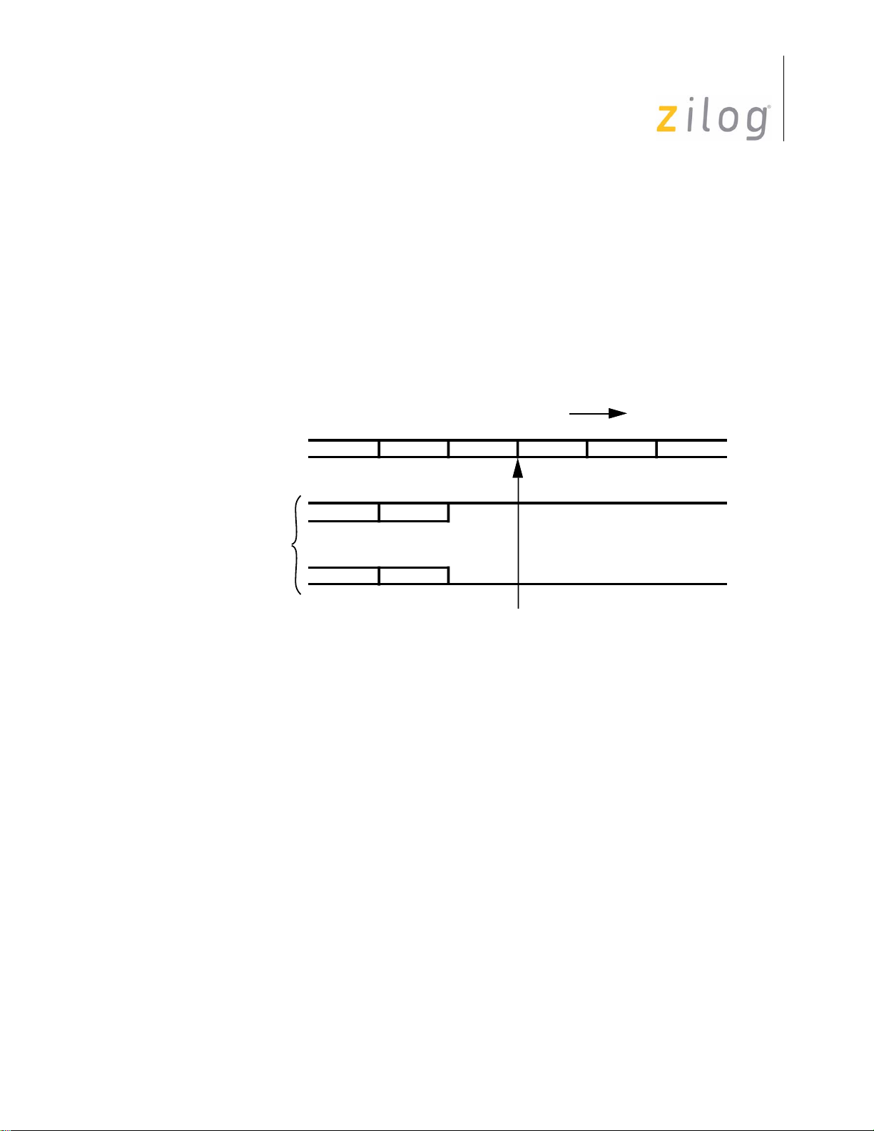
4.3.3 Transmitter/Receiver Synchronization
Receiver Leaves Hunt
Sync
Sync
RxD
TxD
Sync Sync
Direction of message flow
Page 68 of 316
The ISCC contains a transmitter-to-receiver synchronization function that may be used to
guarantee that the character boundaries for the received and transmitted data are the same.
In this mode the receiver is in Hunt and the transmitter is idle, sending either all "1s"" or
all "0s". When the receiver recognizes a sync character, it leaves Hunt mode and one character time later the transmitter is enabled and begins sending sy
point the receiver and transmitter are again completely independent, except that the character boundaries are now aligned. This is shown in Figure 4-10.
ISCC
User Manual
68
nc characters. Beyond this
UM011002-0808
Figure 4–25. Tr ansmitter to Receiver Synchronization
There are several restrictions on the use of this feature in the ISCC. First, it will only work
with 6-bit, 8-bit or 16-bit sync characters, and the data character or eight bits with an 8-bit
or 16-bit sync character. Of course, the receive and transmit clocks must have the same
rate as well as the proper phase relationship.
A specific sequence of operations must be followed to synchronize the transmitter to the
receiver. Both
the receiver and transmitter must have been initialized for operation in Synchronous mode sometime in the past, although this initialization need not be redone each
time the transmitter is synchronized to the receiver. The transmitter is disabled by setting
bit D3 of WR5 to
“0”. At this point the transmitter will send continuous “1s”. If it is
desired that continuous “0s” be transmitted, the Send Break bit (D4) in WR5 should be set
to “1”. The transmitter is now idling but must still be placed in the transmitter to receiver
synchronization mode.
This is accomplished by setting the Loop Mode bit (D1) in WR10 and then enabling the
transmitter by setting bit D3 to WR5 to “1”. At
this point the processor should set the Go
Active on Poll bit (D4) in WR10. The final step is to force the receiver to search for sync
characters. If the receiver is currently disabled the receiver will enter Hunt mode when it is
Page 75

enabled by setting bit D0 of WR3 to “1”. If the receiver is already enabled it may be
Beginning Flag
01111110
8 Bits
Frame
Check
16 Bits
Information
Any Number
Of Bits
Address
8 Bits
Control
8 Bits
Ending Flag
01111110
8 Bits
Frame
Page 69 of 316
placed in Hunt mode by setting bit D4 of WR3 to “1”. Once the receiver leaves Hunt mode
the transmitter is activated on the following character boundary.
4.4 BIT-ORIENTED SYNCHRONOUS MODE
Synchronous Data Link Control mode (SDLC) uses synchronization characters similar to
Bisync and Monosync modes (such as flags and pad characters), but it is a bit-oriented
protocol instead of byte-oriented protocol. High-Level synch ronous Data Link Communication (HDLC) pro-tocol is identical to SDLC except for differences in framing and
handled by the ISCC using the SDLC mode. The discussions on SDLC which follow are
equally applicable to HDLC.
ISCC
User Manual
69
can be
Any data communication link involves at least two stations. The station that
is responsible
for the data link and issues the commands to control the link is called the “primary station”. The other station is a “secondary station”. Not all information transfers need to be
initiated by a primary st
The basic format for SDLC is a “frame” (Figure 4-1
restricted in format
ation. In SDLC mode, a secondary station can be the initiator.
1). The information field is not
or content and can be of any reasonable length (including zero). Its
maximum length is that which can be expected to arrive at the receiver error-free most of
the time. Hence, the determination of maximum length is a function of communication
channel error rate.
Figure 4–26. SDLC Message Format
Two flags that delineate the SDLC frame serve as reference points when positioning the
address and control fields, and they initiate the transmission error check. The ending flag
indicates to the receiving station that the 16-bits just received constitute the frame check.
The ending flag could be followed by another frame, another flag, or an idle. This means
that when two frames follow one another, the intervening flag may simultaneously be the
ending flag of the first frame and the beginning flag of the next frame. Since the SDLC
mode does not use characters of defined length, but rather works on a bit-by-bit basis, the
01111110 (7EH) flag can be recognized at any t ime.
UM011002-0808
To e nsure that the flag is not sent accidentally, SDLC procedures require
a binary “0” to
be inserted by the transmitter after the transmission of any five contiguous “1s”. The
Page 76

ISCC
Page 70 of 316
User Manual
receiver then removes the “0” following a received succession of five “1s”. Inserted and
removed “0s” are not included in the CRC calculation.
There are two unique bit patterns in SDLC mode besides the flag sequence. They are the
Abort and EOP (End of Poll) sequence. An Abort is a sequence of from seven to thirteen
consecutive “1s” and is used to signal the premature termination of a frame. The EOP is
the bit pattern “11111110”, which is used in loop applications as a signal to a secondary
station that it may begin transmission.
70
The address field can consist of one or more octets and is used to designat
e the number of
secondary station to which the commands or data are sent. A control field may follow the
address. The control field is eight bits long and is used to initiate SDLC activities. Data
follows the control field any may consist of any number of bits.
In the SDLC mode, the ISCC operates in the following way. In SDLC mode, frames of
information are opene
d and closed by a flag. The Flag character has the unique bit pattern
of “01111110”. When transmitting data or CRC, the transmitter automatically performs
zero insertion after five consecutive ones, irrespective of character boundaries. In turn, the
receiver searches the receive data stream for five consecutive “1s” and deletes the next bit
if it is a “0”.
CRC may be used in SDLC mode but only with the CRC-CCITT polynomial. In the
SDLC Mode, the transmitter in the SCC cell automatically inverts the
CRC before
trans-mission Because of this inversion, the receiver CRC check results in a non-zero, but
fixed remainder for errorless data. The fixed remainder for this mode is
“0001110100001111” and this is the pattern automatically checked f or in the receiver in
this mode. This is consistent with bit-oriented protocols such as SDLC, HDLC, and
ADCCP.
SDLC mode is selected by setting bit D5 of WR4 to “1” and bits D4, D3,
and D2 of WR4
to “0”. In addition, the flag sequence must be written to WR7. Additional control bits for
SDLC mode are located in WR10.
4.4.1 SDLC Transmit
UM011002-0808
In SDLC mode the transmitter moves characters from the transmit buffer to the shift register, through the zero inserter, and out the TxD pin. The transmitter does not automatically
send the address byte
; it merely encapsulates the data supplied by the processor with flags
and CRC. Also, the processor must load the flag into WR7 as the ISCC does not have a
default flag pattern.
Ordinarily , a frame will be terminated by the ISCC with CRC and a flag but the ISCC may
be programmed
to send an abort and a flag in place of the CRC. This option allows the
ISCC to abort a frame transmission in progress if the transmitter is accidentally allowed to
underrun. This is controlled by the Abort/Flag on Underrun bit (D2) in WR10. When this
bit is set to “1” the transmitter will send an abort and a flag in place of the CRC when an
Page 77

ISCC
Page 71 of 316
User Manual
underrun occurs. The frame will be terminated normally, with CRC and a flag, if this bit is
set to “0”, and the Tx Underrun /EOM latch is reset.
The ISCC is also able to send an abort by command of the processor. The Send Abort
command, issued in WR0, will send eight consecutive “1s” and then the transmitter will
idle. The Send Abort command also empties the transmit buffer register. Since up to five
consecutive “1s” may have been sent prior to the Send Abort command being issued, the
command will cause a sequence of from eight to thirteen “1s” to be transmitted (five ones
of data followed by eight ones of the abort).
71
After the abort when the t
continuous 1’
s instead of idle flags. This option is invoked by setting the Mark/Flag idle
ransmitter enters the idle condition, the ISCC permits sending
bit (D3) in WR10 to “1”. Note that the closing flag will be transmitted correctly even if
this mode is selected.
Before a new frame is transmitted, the Mark/Flag idle bit must be set to “0” to allo
w an
opening flag to be transmitted. The Mark/Flag Idle bit must be set to “0” before data is
written to the transmit buffer . Care must be exercised in doing this because the continuous
“1s” are transmitted, eight at a time (as bytes) by the transmit shift register. After setting
the Mark/Flag Idle bit to “0”, the software must allow time for eight continuous ones to
have left the Transmit Shift register before the first data byte is written to the transmit buffer. This allows the transmitter to recognize that the Flag Idle option has been invoked
seeing an empty transmit buffer, the transmitter will load the flag into the shift regis-
then,
ter for transmission. Once the flag load has been done, the data may be placed in the transmit buffer without disturbing the transmis
transmitter in SDLC mode, all data passes through
sion of the flag. (Note that when using the
the zero inserter, which adds an extra
five bit times of delay between the Transmit Shift register and the Transmit Data pin.)
The number of bits per transmitted character is controlled by bits D6 and D5 of WR5 and
the way the data
is formatted within the transmit buffer. The bits in WR5 allow the option
of five, six, seven, or eight bits per character. When “five bits per character” is selected,
the data must be specially formatted before being written to the transmit buffer. This formatting is shown in Ta ble 4-2. In all cases the data must be right-justified, with the unused
bits being p
rogrammed as per the table (three zeros to the left of the data followed by 1’s
to the left of the zeros to complete the byte).
UM011002-0808
An additional bit, carrying parity information, may be automatically appended to every
transmitted character by setting
bit D6 of WR4 to “1”. This bit is sent in addition to the
number of bits specified in WR4 or by the data format. The parity sense is selected by bit
D1 of WR4. Parity is not normally used in SDLC mode.
The character length may be changed on the fly, but the desired length must be selected
the character is loaded into the transmit shift register from the transmit buffer. The
before
easiest way to ensure this is to write to WR5 to change the character length before writing
the data to the transmit buffer.
Page 78

ISCC
Page 72 of 316
User Manual
Only the CRC-CCITT polynomial may be used in SDLC mode. This is selected by setting
bit D2 in WR5 to “0”. This bit controls the selection for both the transmitter and receiver.
The initial state of the generator and checker is controlled by bit D7 of WR10. When this
bit is set to “1”, both the generator, and checker will have an initial value of all “1s” and, if
this bit is set to “0”, the initial values will be all “0s”.
The ISCC does not automatically preset the CRC generator so this must be done in software. This is accomplished by issuing the Reset Tx CRC generator command, wh
encoded in bits D7 and D6 of WR0. For proper results, this command must be issued
while the transmitter is en-abled and idling. If CRC is to be used the transmit CRC generator must be enabled by setting bit D0 of WR5 to “1”. CRC is normally calculated on all
characters between opening an
tion and never changed.
Enabling the CRC generator is not sufficient to control the transmission of CRC. In the
ISCC this function is controlled by the Tx Underrun/E
processor and set by the ISCC.
d closing flags, so this bit is usually set to “1” at initializa-
OM bit, which may be reset by the
ich is
72
When the transmitter underruns (both the t
empty) the state
If the Tx Underrun/EOM bit is set to “1” when the underrun occurs, the transmitter will
send flags.
The
Reset Tx Underrun/EOM Latch command is encode
is bit is reset to “0” when the underrun occurs, the transmitter will send either the
If th
acc
umulated CRC followed by flags, or an abort followed by flags, depending on the state
of the Abort/Flag on Underrun bit in the WR10, Bit 1. A summary is shown in Table 4-10.
Underrun EOM Bit
Table 4–18. Underrun EOM Bit
Tx Underrun /EOM Latch
Bit
of the Tx Underrun EOM bit determines the action taken by the ISCC.
Abort/Flag
0
0
ransmit buffer and transmit shift register are
d in bits D7 and D6 of WR0.
Action taken by ISCC upon
Transmit Underrun
0
1
Sends CRC followed by flag
Sends abort followed by flag
UM011002-0808
1
The ISCC™ sets the Tx Underrun/EOM Latch when the CRC or abort is loaded into the
shift register for transmission. This event can
x
Sends flag
cause an interrupt, and the status of the Tx
Page 79

ISCC
Page 73 of 316
User Manual
Underrun Latch can be read in RR0. The Tx Underrun Latch may be reset by the processor
via WR0.
For correct transmission of the CRC at the end of a frame, the Reset Tx Underrun/EOM
Latch command must be issued after the first character is written to the ISCC but before
the transmitter underruns after the last character written to the ISCC. The command is usually issued immediately after the first character is written to the ISCC so that the abor
CRC is sent if an underrun occurs inadvertently. The Abort/Flag on Underrun bit (D2) in
WR10 is usually set to “1” at the same time as the Tx Underrun/EOM bit is reset so that an
abort can still be sent if the transmitter underruns. The Abort/Flag on Underrun bit is then
set to “0” near the end of the frame to allow the correct transmission of CRC.
t or
73
In this paragraph the term “complete
ter, not shifted out of the zero inserter, which is an additional five bit times of delay.
SDLC mode, if the transmitter is disabled during transmission of a character, that character will be “completely sent”. This applies to both data and flags. However, if the
trans-mitter is disabled during the transmission of CRC, 16
two CRC bytes will be transmitted but part of the bits will be from the CRC generator and
the latter part of the bits will be from the Flag register rather than form the CRC generator.
Thus part of the CRC bytes will not be transmitted.
There are two modem control signals associated with
ISCC.
The /R TS pin is a simple output that
The /CTS pin is ordinarily a simple input to the CTS bit in RR0. However , if
mode is selected this pin becomes and enable for the transmitter. That is, if Auto Enables
is ON and the /CTS pin is High the transmitter is disabled. If the /CTS pin is Low, the
transmitter is enabled.
The initialization sequence for the transmitter in SDLC mode is: WR4 first, to select the
mode, then
WR5 to select the various options. At this point the other registers should be initialized as
necessary . When all of this is complete, the transmitter may be enabled by setting bit D3 of
WR5 to “1”. Now that the transmitter is enabled, the CRC generator may be initialized by
issuing the Reset Tx CRC Generator command in WR0. A summary is shown in Table 4-
11.
WR10 to modify it if necessary, WR7 to program the flag, and then WR3 and
ly sent” means shifted out of the Transmit Shift regis-
In
total bits corresponding to the
the transmitter provided by the
carries the inverted state of the RTS bi
t (D1) in WR5.
Auto Enables
Table 4–19. Initializing the Transmitter in SDLC Mode
Register Bit No Description
WR5 5-6 Number of bits per character
WR4 1-0 Select parity
WR5 2 Select CRC-CCITT
UM011002-0808
Page 80

Table 4–19. Initializing the Transmitter in SDLC Mode
Page 74 of 316
Register Bit No Description
WR10 7 Select CRC preset value
WR0 6-7 Reset Tx CRC
WR10 1 Abort/flag on underrun
WR0 6-7 Tx underrun
WR7 6-7 Flag
4.4.2 SDLC Receive
ISCC
User Manual
74
The receiver in the ISCC™ always searches the receive data stream for flag characters in
SDLC mode. Ordinarily, the receiver transfers all received data between flags to the
receive data FIFO. However, if the receiver is in Hunt mode no flag is received. The
receiver is in Hunt mode when first enabled, or the receiver may be placed in Hunt mode
by the processor issuing the Enter Hunt mode command in WR3. this bit (D4) is a command, and writing a “0” to it has no effect. The Hunt s
the Sync/Hunt bit in RR0.
Sync/Hunt is one of the possible sources of external/status interrupts, with both transitions
causing an interrupt. This is
issuing the Enter Hunt mode command.
The receiver will automatically enter Hunt mode if
receiver al
Mode when an abort is received, the receiver will always handle frames correctly , and the
Enter Hunt Mode command should never be needed. The ISCC will drive the SYNC pin
Low to signal that a flag has been recognized. The timing for the SYNC signal is shown in
Figure 4-12.
The first byte in an SDLC frame is assumed by the
ary station for which the frame is intended. The ISCC provides several options for handling this address.
ways searches the receive data stream for flags and automatically enters Hunt
true even if the Sync/Hunt bit is set as a result of the processor
tatus of the receiver is reported by
an abort is received. Because the
ISCC to be the address of the
second-
UM011002-0808
Page 81

ISCC
State changes in one
/RTxC clock cycle
/RTxC
PCLK
/SYNC
Page 75 of 316
User Manual
Figure 4–27. /SYNC as an Output
If the Address Search Mode bit (D2) in WR3 is set to “0” the address recognition logic is
disabled and all received frames are transferred to the receive data FIFO. In this mode the
software must perform any address recognition.
75
If the Address Search Mode bit is set to “1”, only those frames whose address ma
tches the
address programmed in WR6 or the global address (all “1s”) will be transferred to the
receive data FIFO.
The address comparison will be across all eight bits of WR6 if the Sync Character Load
inhibit bit (D1) in WR3 is set to “0”. The comparison may be modified so that only the
four most significant bits of WR6 must match the received address. This mode is selected
by setting the Sync Character Load inhibit bit to “1”. In this mode, however, the address
field is still eight bits wide. The address field is transferred to the receive data FIFO in the
same manner as data. It is not treated differently than data.
The number of bits per character is controlled
by bits D7 and D6 of WR3. Five, six, seven,
or eight bits per character may be selected via these two bits. The data is right-justified in
the receive buffer. The ISCC merely takes a snapshot of the receive data stream at the
appropriate times, so the “unused” receive buffer are only the bits following the character.
An additional bit carrying parity information may be selected by setting bit D6 of WR4 to
“1”. This also enables parity in the transmitter
. The parity sense is selected by bit D1 of
WR4. Parity is not normally used in SDLC mode. The character length may be changed at
any time before the new number of bits have been assembled by the receiver. Care should
be exercised, however, as unexpected results may occur. A representative example,
switching from five bits to eight bits and back to five bits is shown in Figure 4-13.
UM011002-0808
Page 82

ISCC
654321
Receive Data Buffer
78
111098761213
19 18 17 16 15 142021
27 26 25 24 23 222829
32 31 30 29 28 273334
37 36 35 34 33 323839
Time
Change from Five to Eight
Change from Eight to Five
5 Bits
5 Bits
5 Bits
8 Bits
8 Bits
Page 76 of 316
User Manual
76
Most bit-oriented protocols allow an arbitrary number of bits between opening and closing flags. The ISCC allows for this by providing three bits of Residue Code in RR1 that
indicates which bits
cessor are actually valid data bits (and not part of the frame check sequence or CRC).
T able 4-12 gives the meanings of the differe
options. The valid data bits are right-justified, that is to say if the number of valid bits
given by the table is less than the character length, then the bits that are valid are the rightmost or least significant bits. It should also be noted that the Residue Code is only valid at
UM011002-0808
the time when the End of Frame bit in RR1 is set to 1.
Figure 4–28. Changing Character Length
in the last three bytes transferred fro the recieve data FIFO by the pro-
nt codes for the four different character length
Page 83

Table 4–20. Residue Codes
Residue Code Bits in Previous Byte Bits in Second Previous Byte Bits in Third Previous Byte
2 1 0 8B/C 7B/C 6B/C 5B/C 8B/C 7B/C 6B/C 5B/C 8B/C 7B/C 6B/C 5B/C
100 0000 3100 8752
010 0000 4200 8763
110 0000 5310 8764
001 0000 6420 8765
101 0000 7531 8765
011 00 0 86 4 87 6
111 10 87 87
000 2 8 8
7 Bits
I-Field CRC Field
Third Previous
Byte
Second Previous
Byte
Previous Byte
Page 77 of 316
As indicated in the table, these bits allow the processor todetermine those bits in the information (and not CRC) field. This allows transparent retransmission of the received frame.
Residue Code bits do not go through a FIFO so they change in RR1 when the last
The
character of the frame is loaded into the receive data FIFO. If there are any characters
already in the receive data FIFO the Residue Code will be updated before they are read by
the processor.
ISCC
User Manual
77
As an example of how the codes are interpreted, conside
r the case of ei
ter and a residue code of 101. The number of valid bits for the previous, second previous,
and third previo
us bytes are 0, 7, and 8 respectively. This indicates that the information
field (I-field) boundary falls on the second previous byte as shown in Figure 4-14.
Figure 4–29. Residue Code 101 Interpretation
A frame is terminated by the detection of a closing flag. Upon detection of the flag the following actions take place: the contents of the Receive Shift Register are transferred to the
receive data FIFO,
the Residue Code is latched, the CRC Error bit is latched and the End
of Frame upon reaching the top of the FIFO can cause a special receive condition. The
processor can then read RR1 to determine the result of the CRC calculation as well as the
Residue Code.
Only the CRC-CCITT polynomial may be used for CRC calculation in SDLC mode,
UM011002-0808
although the generator and checker may be preset to all “1s” or all “0s”. The CRC-CCITT
polynomial is selected by setting
bit D2 of WR5 to “0”, bit D7 of WR10 controls the pre-
ght bits per charac-
Page 84

ISCC
Page 78 of 316
User Manual
set value. If this bit is set to “1”, the generator and checker are preset to “1s”, if this bit is
reset, the generator and checker are present to all “0s”.
The receiver expects the CRC to be inverted before trans-mission and so checks the CRC
result aga inst the value “ 0001110100001111”. The ISCC pr esets the CRC checker whenever the receiver is in Hunt mode or whenever a flag is received so a CRC reset command
is not strictly necessary. Ho
wever, the CRC checker may be preset by issuing the Reset
CRC Checker command in WR0.
78
The CRC checker is automatically enabled for all data between
the opening and closing
flags by the SCC cell in SDLC mode, and the Rx CRC Enable bit (D3) in WR3 is ignored.
The result of the CRC calculation for the entire frame is valid in RR1 only when accompanied by the End of Frame bit being set in RR1. At all other times the CRC Error bit in RR1
should be ignored by the processor
Care must be exercised so that the processor does not
.
attempt to use the CRC
bytes that
are transferred as data because not all of the bits are transferred properly. The last two bits
of CRC are never transferred to the receive data FIFO and are not recoverable.
Note the following about ISC
C CRC operation:
The normal CRC checking mechanism involves checking over data and CRC characters.
If the division remainder is 0, there is no CRC error
SDLC is dif
ferent. The CRC generator, when receiving a correct frame, will have a fix
.
ed,
non-zero remainder. The actual remainder in the receive CRC calculation must be checked
against this fixed value to determine if a CRC error exists.
A frame is terminated by a closing flag. When the ISCC recognizes this flag:
The contents of the Receive Shift register are transferred to the receive data FIFO.
The Residue Code is latched, and the CRC Error bit is latched in the status FIFO and the
End of Frame bit is set in the receive status FIFO.
The End of Frame bi
t, upon reaching the top of the FIFO,
will cause a special rece
ive condition. The processor may then read RR1 to determine the result of the CRC calculation as
well as the Residue Code. If either the Rx Interrupt or Special Condition Only or th
e Rx
Interrupt on First Character or Special Condition modes are selected, the FIFO will be
locked, and the processor must issue an Error Reset command in WR0 to unlock the
receive FIFO.
UM011002-0808
In addition to searching the data stream for flags, the receiver in the ISCC also watches for
seven consecutive “1s”, whic
h is the abort condition. The presence of seven consecutive
“1s” is reported in the Break/Abort bit in RR0. This is one of the possible external/status
interrupts, so transitions of this status may be programmed to cause interrupts. Upon
receipt of an abort the receiver is forced into Hunt mode where it looks for flags. The Hunt
status is also a possible external/status condition whose transition may be programmed to
cause an interrupt. The transitions of these two bits occur very close together but either
one or two external/status interrupts may result. The abort condition is terminated when a
Page 85

ISCC
Page 79 of 316
User Manual
“0” is received, either by itself or as the leading “0” of a flag. The receiver does not leave
Hunt mode until a flag has been received so two discrete external/status conditions will
occur at the end of an abort. An abort received in the middle of a frame terminates the
frame reception, but not in an orderly manner, because the character being assembled is
lost.
Up to two modem control signals associated with the receiver are available in SDLC
mode:
The /DTR//REQ pin carries inverted state of the DTR bit (D7) in WR5 unless this pin has
been
programmed to carry a DMA Request signal.
79
The /DCD pin is ordinarily a simple input to the DCD bit in RR0. However
Enables mode is selected by setting bit D5 of WR3 to “1”, this pin becomes an enable for
receiver. That is, if Auto Enable is on and the /DCD pin is High the receiver is dis-
the
abled. While the /DCD pin is Low, the receiver is enabled.
The initialization sequence for the receiv
mode
, then WR10 to modify it if necessary, WR6 to program the address, WR7 to program the flag and WR3 and WR5 to select the various options. At this point the other registers should be initialized as necessary . When all of this is completed the receiver may be
enabled by
Initializing the Receiver in SDLC Mode
setting bit 0 of WR3 to a one. A summary is shown in Table 4-13.
Table 4–21. Initializing the Receiver in SDLC Mode
er in SDLC mode is WR4 first, to select the
, if the Auto
Register Bit No Description
WR3 6-7 Number of bits per character
WR4 0-1 Select parity
WR5 2 Select CRC-CCITT Generator
WR10 7 Select CRC preset value
5-6 Select NRZ/NRZI encoding
WR5 7 DTR/REQ
WR6 0-7 Address
WR7 0-7 Flag
WR3 5 Auto enable
UM011002-0808
Page 86

The receiver searches for synchronization when it is in Hunt mode. In this mode the
Notes:
Page 80 of 316
receiver is idle except that it is searching the data stream for a flag match.
When the receiver detects a flag match it achieves synchronization and interprets the following byte as the address field.
The SYNC/HUNT bit in RR0 reports the Hunt Status and an interrupt can be generated
upon transitions between the Hunt state and the Sync state.
The ISCC will drive the /SYNC pin Low to signal that the flag has been received.
4.4.3 SDLC LOOP MODE
The ISCC supports SDLC Loop mode in addition to normal SDLC. SDLC Loop mode is
very similar to normal SDLC but is usually used in applications where a point-to-point
network is not appropriate (for example, Point-of-Sale terminals). In an SDLC Loop there
is a primary controller that manages the message traffic flow on the loop and any number
of secondary stations. In SDLC Loop mode, the ISCC operating in regular SDLC mode
can act as the primary controller.
ISCC
User Manual
80
A secondary station in an SDLC Loop is always listening to the messages being sent
around the loop, and in fact must pass these messages to the rest of the loop by retransmitting them with a one-bit-time delay.
The secondary station can place its own message on the loop only at specific times. The
controller signals that secondary stations may transmit messages by sending a special
character, called an EOP (End of Poll), around the loop. The EOP character is the bit pattern 11111110.
When a secondary station has a message to transmit and recognizes an EOP on the line, it
changes the last binary 1 of the EOP to a 0 before transmission. This has the effect of turning the EOP into a flag pattern. The secondary station now places its message on the loop
and terminates its message with an EOP. Any secondary stations further down the loop
with messages to transmit can append their messages to the message of the first secondary
station by the same process.
All secondary stations without messages to send merely echo the incoming messages and
are prohibited from placing messages on the loop, except upon recognizing an EOP.
SDLC Loop mode is quite similar to normal SDLC mode except that two additional control bits are used. Writing a 1 to the Loop Mode bit in WR10 configures the ISCC for
Loop mode. Writing a 1 to the Go Active on Poll bit in the same register normally causes
the ISCC to change the next EOP into a flag and then begin transmitting on loop. However, when the ISCC first goes on loop it uses the first EOP as a sign al to insert the one-bit
UM011002-0808
Page 87

ISCC
Page 81 of 316
User Manual
delay, and doesn’t be-gin transmitting until it receives the second EOP. There are also two
additional status bits in RR10, the On Loop bit and the Loop Sending bit.
There are also restrictions as to when and how a secondary station physically becomes part
of the loop.
A secondary station that has just powered up must monitor the loop, without the one-bittime delay, until it recognizes an EOP. When an EOP is recognized the one-bit-time de-lay
is switched on. This does not disturb the loop because the line is marking idle between the
time that the controller sends the EOP and the time that it receives the EOP back. The secondary station that has gone on-loop cannot place a message on the loop until the next
time that an EOP is issued by the controller. A secondary station goes off-loop in a similar
manner. When given a command to go off-loop, the secondary station waits until the next
EOP to remove the one-bit-time delay.
81
To operate the ISCC in SDLC Loop mode, the ISCC must first be programmed just as if
normal SDLC were to be used. Loop mode is then selected by writing the appropriate control word in WR10; the ISCC is now waiting for the EOP so that it can go on loop. While
waiting for the EOP, the ISCC ties TxD to RxD with only the internal gate delays in the
signal path. When the first EOP is recognized by the ISCC, the Break/Abort/EOP bit is set
in RR0, generating an External/Status interrupt (if so enabled). At the same time, the OnLoop bit in RR10 is set to indicate that the ISCC is indeed on-loop, and a one-bit time
delay is inserted in the TxD to the RxD path.
The ISCC is now on-loop but cannot transmit a message until a flag and the next EOP are
received. The requirement that a flag be received ensures that the ISCC cannot erroneously send messages until the controller ends the current polling sequence and starts
another one.
If the CPU in the secondary station with ISCC needs to transmit a message, the GoActive-On-Poll bit in WR10 must be set. If this bit is set when the EOP is detected, the
ISCC changes the EOP to a flag and starts sending another flag. The EOP is reported in
the Break/Abort/EOP bit in RR0 and the CPU should write its data bytes to the ISCC, just
as in normal SDLC frame transmission. When the frame is complete and CRC has been
sent, the ISCC closes with a flag and reverts to One-Bit-Delay mode. The last zero of flag,
along with the marking line echoed from the RxD pin, form an EOP for secondary stations
further down the loop.
UM011002-0808
While the ISCC is actually transmitting a message, the loop-sending bit in R10 is set to
indicate this.
If the Go-Active-On-Poll bit is not set at the
time the EOP pa
sses by,
the ISCC cannot
send a message until a flag (terminating the current polling sequence) and another EOP are
received.
Page 88

ISCC
Page 82 of 316
User Manual
If SDLC loop is deselected, the ISCC is designed to exit from the loop gracefully. When
SDLC Loop mode is deselected by writing to WR10; the ISCC waits until the next polling
cycle to remove the one-bit time delay.
If a polling cycle is in progress at the time the command is written, the ISCC finishes
sending any message that it may be transmitting, ends with an EOP, and disconnects TxD
from RxD. If no message was in progress, the ISCC immediately disconnects TxD from
RxD.
82
Once the ISCC™ is not sending on the loop, an exit from the loop is ac
complished by setting the Loop Mode bit in WR10 to “0”, and at the same time writing the Abort/Flag on
Underrun and Mark/Flag idl
e bits with the desired values. The ISCC will revert to normal
SDLC operation as soon as an EOP is received, or immediately, if the receiver is already
in Hunt mode because of the receipt of an EOP.
To ensure proper loop operation after the ISCC goes off the loop, and until the external
relays
take the ISCC completely out of the loop, the ISCC should be programmed for
Mark idle instead of Flag idle. When the ISCC goes off the loop, the On-Loop bit is reset.
Note: With NRZI encoding, removing the stations from the loop (removing the one-bit
time delay) may cause problems further down the loop because of extraneous transitions
on the line. The ISCC avoids this problem by making transparent adjustments at the end of
each frame it sends in response to an EOP. A response frame from the ISCC is terminated
by a flag and EOP. Normally, the flag and the EOP share a zero, but if such sharing would
cause the RxD and TxD pins to be of opposite polarity after the EOP, the ISCC adds
another zero between the flag and the EOP. This causes an extra line transition so that RxD
and TxD are identical after the EOP is sent. This extra zero is completely transparent
because it only means that the flag and the EOP no longer share a zero. All that a proper
loop exit needs, therefore, is the removal of the one-bit delay.
The ISCC allows the user the option of using NRZI in SDLC Loop mode by programming
WR10 appropriately. With NRZI encoding, the outputs of secondary stations in the loop
may be inverted from their inputs because of messages that they have transmitted.
UM011002-0808
The initialization sequence for the SCC cell in SDLC Loop mode is similar to
sequence used in SDLC mode, except
that it is somewhat longer. The processor should
the
program WR4 first, to select SDLC mode, and then WR10 to select the CRC preset value
and program the Mark/Flag idle bit. The Loop Mode and Go Active On Poll bits in WR10
should not be set to “1” yet. The flag is written in WR7 and the various options are
selected in WR3 and WR5. At this point the other registers should be initialized as necessary, as shown in Table 4-14.
Page 89

ISCC
Page 83 of 316
User Manual
83
Table 4–22. SDLC Loop Mode Initialization
Register Bit No Description
WR4 5-4 Select SDLC mode
WR10 7 Select CRC preset value
3 Select mark/flag idle bit
WR7 Flag
WR3 7-6 Select bits per character for receiver
1 Sync character load inhibit
2 Address search mode
5 Auto enables
WR5 6-5 Select bits per character for transmitter
4 Send break
2 Select SDLC CRC
7
1
WR4 1-0 Select parity
7-6 Select clock mode
WR6 0-7 Address
WR10 6-5 Select data encoding
Then the Loop Mode bit (D1) in WR10 should be set to “1”. When all of this is complete
the transmitter may be enabled by setting bit D3 of WR5 to “1”. Now that the transmitter
is enabled, the CRC generator may be initialized by issuing the Reset Tx CRC Generator
command in WR0. The receiver is enabled by setting the Go Active on Poll bit (D4) in
WR10 to “1”. The ISCC will go on the loop when seven consecutive “1s” are received,
and will signal this by setting the On Loop bit in RR10. Note that the seven consecutive
“1s” will set the Break/Abort and Hunt bits in RR0 also. Once the ISCC is on the loop, the
Go Active on Poll bit should be set to “0” until a message is to be transmitted on the loop.
To transmit a message on the loop, the Go Active on Poll bit should be set to “1”. At this
UM011002-0808
Page 90

point the processor may either write the first character to the transmit buffer and wait for a
Page 84 of 316
transmit buffer empty condition, or wait for the Break/Abort and Hunt bits to be set in
RR10 and the Loop Sending bit to be set in RR10 before writing the first data to the trans
mitter. The Go Active On Poll bit should be set to “0” after the transmission of the frame
gun. To go off of the loop, the processor should set the Go Active On Poll bit in
has be
WR10 to “0” and then wait for the Loop Sending bit in RR10 to be set to “0”. At this point
the Loop Mode bit (D1) in WR10 is set to “0” to request an orderly exit from the loop. The
ISCC will exit SDLC Loop mode when seven consecutive “1s” have been received; at the
same time the Break/Abort and Hunt bits in RR0 will be set to “1”, and the On Loop bit in
RR10 will be set to “0”.
4.4.4 SDLC Loop Mode Receive
SDLC Loop mode is quite similar to SDLC mode except that two additional control bits
are used. They are the Loop Mode bit (D1) and the Go Active on Poll bit (D4) in WR10.
In addition to these two extra control bits, there are also two status bits in RR10. They are
the On Loop bit (D1) and the Loop Sending bit (D4).
ISCC
User Manual
84
-
Before Loop mode is selected both the receiver and transmitter must be completely
ized for SDLC operation. Once this is done, Loop mode is selected by setting bit D1 of
WR10 to “1”. At this point the ISCC connects TxD to RxD
path. At the same time a flag is loaded into the Transmit Shift register, and is shifted to the
end of the zero inserter, ready for transmission. The ISCC wil l remain in this state until the
Go Active on Poll bit (D4) in WR10 is set to “1”. When this bit is set to “1” the receiver
begins looking for a sequence of seven consecutive “1s”, indicating either an EOP or an
idle line. When the receiver detects this condition the Break/Abort bit in RR0 is set to “1”
and a one-bit time delay is inserted in the path from RxD to TxD. The On Loop bit in
RR10 is also set to “1” at this time, and the receiver enters the Hunt mode. The ISCC cannot transmit on the loop until a flag is received, causing the rece
and another EOP (bit pattern “11111110”) is received. The ISCC is now on the loop and
capable of transmitting on the loop. As soon as this status is recognized by the processor,
the Go Active On Poll bit in WR10 should be set to “0” to prevent the ISCC from transmitting on the loop without the consent of the processor.
4.4.5 SDLC Loop Mode Transmit
T o transmit a message on the loop, the Go Active On Poll bit in WR10 must be set to “1”.
Once this is done, the ISCC will change the next received EOP into a Flag and begin transmitting on the loop.
When the EOP is received, the Break/Abort and Hunt bits in RR0 will be set to “1”, and
the Loop Sending bit in RR10
ten after the Go Active On Poll bit has been set or
will also be set to “1”. Data to be transmitted may be writ-
initial-
with only gate delays in the
iver to leave Hunt mode,
after the receiver enters Hunt mode.
UM011002-0808
Page 91

ISCC
Page 85 of 316
User Manual
If the data is written immediately after the Go Active On Poll bit has been set, the ISCC
will only insert one flag after the EOP is changed into a flag. If the data is not written until
after the receiver enters the Hunt mode, the flags will be transmitted until the data is writ
ten. If only one frame is to be transmitted on the loop in response to an EOP, the processor
must set the Go
Active on Poll bit to “0” before the last data is written to the transmitter . In
this case the transmitter will close the frame with a single flag, and then revert to the onebit delay . The Loop Sendi ng bit in RR10 is set to “0” when the closing Flag has been sent.
If more than one frame is to be transmitted, the Go Active On Poll bit should not be set to
“0” until the last frame is being sent. If this bit is not set to “0” before the end of a frame,
the transmitter will send Flags until either more data is written to the transmitter, or until
the Go Active On Poll bit is set to “0”. Note that the state of the Abort/Flag on Underrun
and Mark/Flag idle bits in WR10 are ignored by the ISCC in SDLC Loop mode.
85
-
UM011002-0808
Page 92

Chapter 5 Register Descriptions
Page 86 of 316
5.1 INTRODUCTION
This section describes the function of the various bits in the registers of the device.
Throughout this section the following conventions will be used:
Control bits may be written and read by the CPU and will not be modified by the device.
Command bits may be written by the CPU to initiate an action in the device and will be
read as zeros. Status bits are controlled by the device and may be read to check device status. Any writes to status bits are ignored by the device. Command/status bits are controlled
by both the device and the CPU. They may be written and read by the CPU and may also
be modified by the device.
ISCC
User Manual
86
Reserved bits are not used in this implementation of the device and may or may not be
physically present in the device. Reserved bits that are physically present will be readable
and writable but reserved bits that are not present will always be read as zero. To ensure
compatibility with future versions of the device reserved bits should always be written
with zeros. Reserved commands should not be used for the same reason.
5.2 REGISTER DESCRIPTIONS
Register can be accessed through either channel, the Interrupt Vector Read Register
returns the interrupt vector with status if read from Channel B and without status if read
from Channel A, and Channel A has an additional read register which contains all the
Interrupt Pending bits.
5.2.1 Write Registers, SCC Cell
Ten write regist ers are used for control, two for sync character generation, and two for
baud rate generation. In addition, there are two write registers which are shared by both
channels; one is the interrupt vector register, and one is the master interrupt control and
reset register. See Table 5-1 for a summary on write registers.
Table 5–23. SCC Cell Write Registers
Register Description
WR0 Register Pointers, various initialization commands
WR1 Transmit and Receive interrupt enables, commands WAIT/DMA
WR2 Interrupt Vector
UM011002-0808
Page 93
Table 5–23. SCC Cell Write Registers (Continued)
Page 87 of 316
Register Description
WR3 Receive parameters and control modes
WR4 Transmit and Receive modes and parameters
WR5 Transmit parameters and control modes
WR6 Sync Character or SDLC address
WR7 Sync Character or SDLC flag
WR8 Transmit buffer
WR9 Master Interrupt control and reset commands
ISCC
User Manual
87
WR10 Misc. transmit and receive control bits
WR11 Clock mode controls for receive and transmit
WR12 Lower byte of baud rate generator
WR13 Upper byte of baud rate generator
WR14 Miscellaneous control bits
WR15 External status interrupt enable control
5.2.2 Read Registers, SCC Cell
Four read registers indicate status information, two are for baud rate generation, and one
for the receive buffer. In addition, there are two read registers which are shared by both
channels: one for the interrupt pending bits and one for interrupt vector. See Table 5-2 for
a summary on the SCC cell read registers.
Table 5–24. SCC Cell Read Registers
Register Description
RR0 Transmit and Receive buffer status and external status
RR1 Special Receive Condition status
RR2 Modified interrupt vector (Channel B only), Unmodified interrupt
vector (Channel A only)
UM011002-0808
Page 94
User Manual
Page 88 of 316
Table 5–24. SCC Cell Read Registers
Register Description
RR3 Interrupt pending bits (Channel A only)
RR6 SDLC FIFO byte counter lower byte (only when enabled)
RR7 SDLC FIFO byte count and status (only when enabled)
RR8 Receive buffer
RR10 Miscellaneous status bits
RR12 Lower byte of baud rate generator time constant
RR13 Upper byte of baud rate generator time constant
ISCC
88
RR15 External Status interrupt information
5.2.3 DMA Registers
The DMA cell contains 16 read write registers for control of the DMA channels. The
DMA possesses its own interrupt vector register and interrupt control registers which are
independent of the SCC cell. The DMA cell also includes the Bus Configuration Register
(BCR) for the ISCC. The addresses, names and descriptions of these registers are given in
Table 5-3.
Table 5–25. DMA Cell Register Description
Address Name Description
xxxxx BCR Bus Configuration Register
00000 CCAR Channel Command/AddressRegister (Write)
00000 DSR DMA Status Register (Read)
00001 ICR Interrupt Control Register
00010 IVR Interrupt Vector Register
00011 ICSR Interrupt Command Register (Write)
00011 ISR Interrupt Status Register (Read)
00100 DER DMA Enable/Disable Register
UM011002-0808
Page 95

ISCC
Page 89 of 316
User Manual
Table 5–25. DMA Cell Register Description
Address Name Description
00101 DCR DMA Control Register
00110 Reserved Address
00111 Reserved Address
01000-01001 RDCRA Receive DMA Count Register Channel A (Low-
high byte)
01010-01011 TDCRA Transmit DMA Count Register Channel A
01100-01101 RDCRB Receive DMA Count Register Channel B
89
01110-01111 TDCRB Transmit DMA Count Register Channel B
10000-10011 RDARA Receive DMA Address Register Channel A
10100-10111 TDARA Transmit DMA Address Register Channel A
11000-11011 RDARB Receive DMA Address Register Channel B
11100-11111 TDARB Transmit DMA Address Register Channel B
5.3 SCC CELL REGISTER OVERVIEW
The SCC cell write register set in each channel includes ten control registers (among them
is the transmit buffer), two sync character registers and two baud rate time constant registers. The interrupt control register and the master interrupt control and reset register are
shared by both channels.
The only variation in register definition is between the multiplexed and non-multiplexed
bus mode programming of the ISCC. The variation exists in the command decode structure; register WR0. The following sections describe in detail each write register and the
associated bit configuration for each.
5.4 WRITE REGISTERS
The following sections describe WR registers in detail.
UM011002-0808
Page 96

5.4.1 Write Register 0 (Command Register)
Write Register 0 (non-multiplexed bus mode)
D6D7
D5 D4 D3 D2 D1 D0
Register 0
Register 1
Register 2
Register 3
Register 4
Register 5
Register 6
Register 7
Register 8
Register 9
Register 10
Register 11
Register 12
Register 13
Register 14
Register 15
0
0
1
1
0
0
1
1
0
0
1
1
0
0
1
1
0
1
0
1
0
1
0
1
0
1
0
1
0
1
0
1
0
0
0
0
1
1
1
1
0
0
0
0
1
1
1
1
Null Code
Point High
Reset Ext/Status Interrupts
Send Abort (SDLC)
Enable Int on Next Rx Character
Reset Tx Int Pending
Error Reset
Reset Highest IUS
0
0
1
1
0
0
1
1
0
1
0
1
0
1
0
1
0
0
0
0
1
1
1
1
Null Code
Reset Rx CRC Checker
Reset Tx CRC Generator
Reset Tx Underrun/EOM Latch
0
0
1
1
0
1
0
1
* With Point High Command
*
Page 90 of 316
WR0 is the command register and the CRC reset code register. WR0 takes on slightly different forms depending upon whether the ISCC is in the multiplexed or non-multiplexed
bus mode of operation. Figure 5-1 shows the bit configuration for the non-multiplexed
mode and includes register select bits in addition to command and reset codes.
ISCC
User Manual
90
UM011002-0808
Figure 5–30. WR0 in the Non-Multiplexed Bus Mode
Page 97

ISCC
Null Code
Null Code
Select Shift Left Mode
Select Shift Right Mode
Null Code
Null Code
Reset Ext/Status Interrupts
Send Abort
Enable Int on Next Rx Character
Reset Tx Int Pending
Error Reset
Reset Highest IUS
Null Code
Reset Rx CRC Checker
Reset Tx CRC Generator
Reset Tx Underrun/EOM Latch
Write Register 0 (multiplexed bus mode)
D6D7
D5 D4 D3 D2 D1 D0
0
0
1
1
0
0
1
1
0
1
0
1
0
1
0
1
0
0
1
1
0
1
0
1
0
0
1
1
0
1
0
1
0
*
0
0
0
0
1
1
1
1
* B Channel Only
Page 91 of 316
User Manual
Figure 5-2 shows the bit configuration for the multiplexed mode and includes (in Channel
B only) the address decoding select described later.
91
UM011002-0808
Figure 5–31. WR0 in the Multiplexed Bus Mode
The following bit description for WR0 is identical for both versions except where specified.
Bits D7 and D6 are the CRC Reset Codes 1 and 0.
Bit combination 00 is a Null Command
This command has no effect on the ISCC SCC cell and is used when a write to WR0 is
necessary for some reason other than a CRC Reset command.
Bit combination 01 is the Reset Receive CRC Checker Command
This command is used to initialize the receive CRC circuitry. It is necessary in synchronous modes (except SDLC) if the Enter Hunt Mode command in Write Register 3 is not
issued between received messages. Any action that disables the receiver initializes the
CRC circuitry. Resetting the Receive CRC Checker command is accomplished automatically in SDLC mode.
Page 98

ISCC
Page 92 of 316
User Manual
Bit combination 10 is the Reset Transmit CRC Generator Command
This command initializes the CRC generator. It is usually issued in the initialization routine and after the CRC has been transmitted. A Channel Reset will not initialize the generator and this command should not be issued until after the transmitter has been enabled in
the initialization routine.
Bit combination 11 is the Reset Transmit Under-run/EOM Latch Command
This command controls the transmission of CRC at the end of transmission (EOM). If this
latch has been reset, and a transmit underrun occurs, the SCC cell automatically appends
CRC to the message. In SDLC mode with Abort on Underrun selected, the SCC cell sends
an abort, and Flag on underrun if the TX Underrun/EOM latch has been reset.
At the start of the CRC transmission, the Tx Underrun/EOM latch is set. The Reset command can be issued at any time during a message. If the transmitter is disabled, this command will not reset the latch. However, if no External Status interrupt is pending, or if a
Reset External Status interrupt command accompanies this command while the transmitter
is disabled, an External/Status interrupt is generated with the Tx Underrun/EOM bit reset
in RR0.
92
Bits D5-D3 are the Command Codes for the SCC Cell.
Bit combination 000 is a Null Command.
The Null command has no effect on the SCC.
Bit combination 001 is the Point High Command
This command effectively adds eight to the Register Pointer (D2-D0) by allowing WR8
through WR15 to be accessed. The Point High command and the Register Pointer bits are
written simultaneously. This command is used when the ISCC is configured to be in the
non-multiplexed bus mode. Note that WR0 changes form depending upon the bus mode
selection.
Bit combination 010 is the Reset External/Status Interrupts Command
After an External/Status interrupt (a change on a modem line or a break condition, for
example), the status bits in RR0 are latched. This command re-enables the bits and allows
interrupts to occur again as a result of a status change. Latching the status bits captures
short pulses until the CPU has time to read the change.
The SCC cell contains simple queueing logic associated with most of the external status
bits in RR0. If another External/Status condition changes while a previous condition is
still pending (Reset External/Status Interrupts has not yet been issued) and this condition
persists until after the command is issued, this second change causes another External/Status interrupt. However, if this second status change does not persist (there are two transitions), another interrupt is not generated. Exceptions to this rule are detailed in the RR0
description.
UM011002-0808
Page 99

ISCC
Page 93 of 316
User Manual
Bit combination 011 is the Send Abort Command
This command is used in SDLC mode to transmit a sequence of eight to thirteen “1s.” This
command always empties the transmit buffer and sets Tx Underrun/EOM bit in Read Register 0.
Bit combination 100 is the Enable Interrupt On Next Rx Character Command
If the interrupt on First Received Character mode is selected, this command is used to
reactivate that mode after each message is received. The next character to enter the receive
FIFO causes a Receive interrupt. Alternatively, the first previously stored character in the
FIFO will cause a Receive interrupt.
Bit combination 101 is the Reset Tx Interrupt Pending Command
This command is used in cases where there are no more characters to be sent; e.g., at the
end of a message. This command prevents further transmit interrupts until after the next
character has been loaded into the transmit buffer or until CRC has been completely sent.
This command is necessary to prevent the transmitter from requesting an interrupt when
the transmit buffer becomes empty (with Transmit Interrupt Enabled).
93
Bit combination 110 is the Error Reset Command
This command resets the error bits in RR1. If interrupt on first Rx Character or interrupt
on Special Condition modes are selected and a special condition exists, the data with the
special condition is held in the receive FIFO until this command is issued. If either of
these modes is selected and this command is issued before the data has been read from the
receive FIFO, the data is lost.
Bit combination 111 is the Reset Highest IUS Command
This command resets the highest priority Interrupt Under Service (IUS) bit, allowing
lower priority conditions to request interrupts. This command allows the use of the internal daisy-chain (even in systems without an external daisy-chain) and should be the last
operation in an interrupt service routine.
Bits 2 through 0 are the Register Selection Code when the device is programmed to be in
the non-multiplexed bus mode. These three bits select Registers 0 through 7. With the
Point High command, Registers 8 through 15 are selected.
In the multiplexed bus mode, bits D2 through D0 have the following function.
Bit D2 must be programmed as “0.” Bits D1 and D0 select Shift Left/Right; that is
WR0(1-0)=10 for shift left and WR0(1-0)=11 for shift right.
UM011002-0808
Page 100

ISCC
Page 94 of 316
User Manual
5.4.2 Write Register 1 (Transmit/Receive Interrupt and Data Transfer Mode Definition)
Write Register 1 is the control register for the various SCC cell interrupt and Wait/Request
modes. Figure 5-3 shows the bit assignments for WR1.
Table 5–26. SCC Cell Register Address Map using Pointer (Non-Multiplexed Bus Mode)
Using Null Command
A1/A//B Address D2 D1 D0 Write Register Read Register
0 000 WR0B RR0B
0 001 WR1B RR1B
0 010 WR2 RR2B
0 011 WR3B RR3B
94
0 100 WR4B (RR0B)
0 101 WR5B (RR1B)
0 110 WR6B (RR2B)
0 111 WR7B (RR3B)
1 000 WR0A RR0A
1 001 WR1A RR1A
1 010 WR2 RR2A
1 011 WR3A RR3A
1 100 WR4A (RR0A)
1 101 WR5A (RR1A)
1 110 WR6A (RR2A)
1 111 WR7A (RR3A)
Using Point High Command
A1/A//B Address D2 D1 D0 Write Register Read Register
0 000 WR8B RR8B
0 001 WR9 (RR13B)
0 010 WR10B RR10B
UM011002-0808
 Loading...