


1
Z08617 NMOS Z8
®
8-BIT MCU
KEYBOARD CONTROLLER
FEATURES
C
USTOMER PROCUREMENT
S
PECIFICA TION
■ Low Power Consumption - 750 mW
■ 32 Input/Output Lines
■ Digital Inputs NMOS Levels with
Internal Pull-Up Resistors
■ 4 Kbytes ROM
■ Four Direct Connect LED Drive Pins
■ 124 Bytes of RAM
■ Hardware Watch-Dog Timer (WDT)
■ Two Programmable 8-Bit Counter/Timers,
Each with 6-Bit Programmable Prescaler
■ Six Vectored, Priority Interrupts from
Six Different Sources
■ On-Chip RC Oscillator
■ Clock Frequency: Up to 5MHz
■ Low EMI Emission
GENERAL DESCRIPTION
The Z08617 Keyboard Controller is a member of the
Z8® single-chip microcontroller family with 4 Kbytes
of ROM. The device is housed in a 40-pin DIP package,
and is manufactured in NMOS technology. The Z08617
microcontroller offers fast execution, efficient use of
memory, sophisticated interrupt, input/output bitmanipulation capabilities, and easy hardware/software system expansion along with low cost and low
power consumption.
The Z08617 architecture is characterized by a flexible I/O scheme, an efficient register, I/O, and a
number of ancillary features that are useful in many
industrial and advanced scientific applications.
For applications which demand powerful I/O capabilities, the Z08617 provides 32 pins dedicated to input
and output. These lines are grouped into four ports,
each port consists of 8 lines, and are configurable
under software control to provide timing, status
signals, and serial or parallel I/O ports.
The Z08617 offers low EMI emission which is achieved
by means of several modifications in the output
drivers and clock circuitry of the device.
There are two basic address spaces which are available to support this wide range of configurations:
Program Memory and 124 General-Purpose Registers.
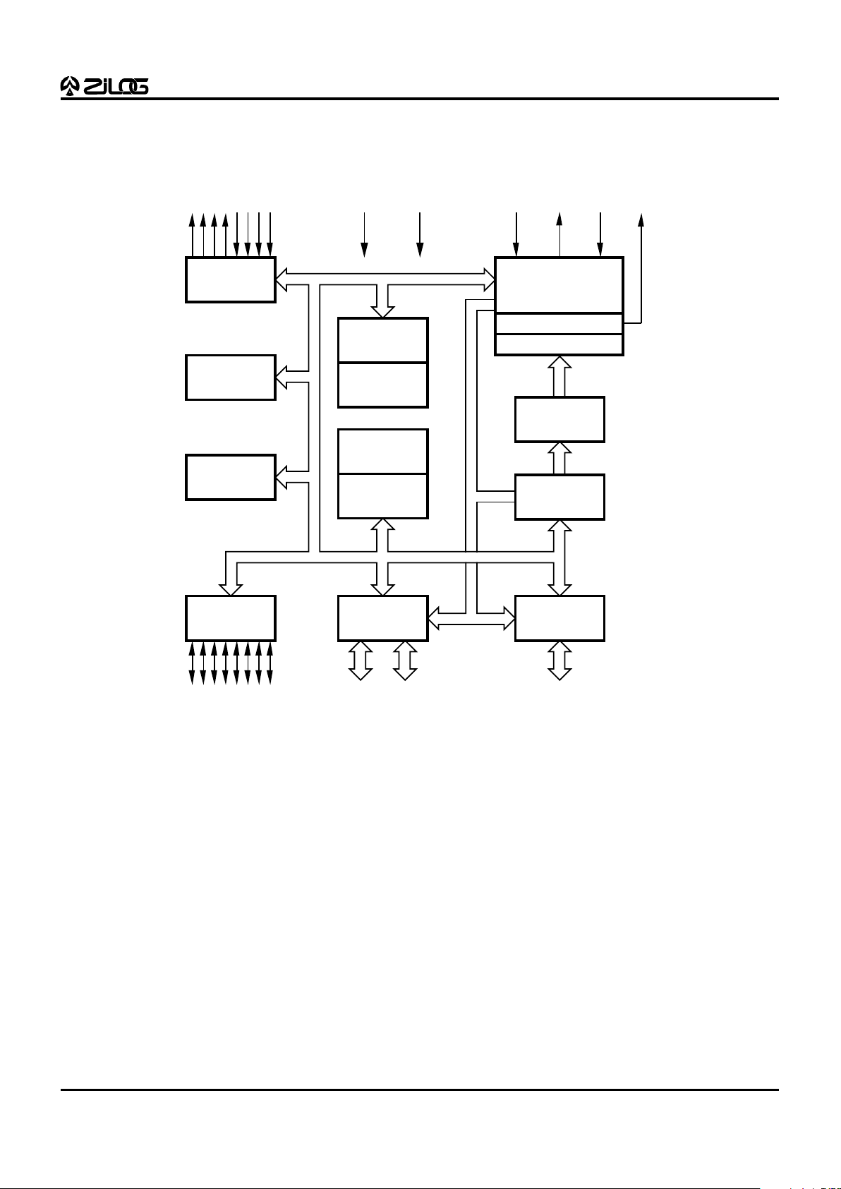
The Z08617 offers two on-chip counter/timers with
a large number of user-selectable modes. This unburdens the program from coping with real-time problems such as counting/timing (Figure 1).
Notes:
All Signals with a preceding front slash, "/", are active Low,
e.g., B//W (WORD is active Low); /B/W (BYTE is active Low,
only).
Power connections follow conventional descriptions below:
Connection Circuit Device
Power V
CC
V
DD
Ground GND V
SS
DS96KEY0300
Z08617
NMOS Z8® 8-BIT MCU
KEYBOARD CONTROLLER
Z08617 NMOS Z8
®
8-BIT MCU
KEYBOARD CONTROLLER
2
GENERAL DESCRIPTION (Continued)
Port 3
Counter/
Timers (2)
Interrupt
Control
Port 2
I/O
(Bit Programmable)
ALU
Flags
Register
Pointer
Register File
124 x 8-Bit
Machine Timing
& Instruction Control
Program
Memory
Program
Counter
Vcc GND
Output Input
Port 0 Port 1
I/O
Output Open-Drain
(Nibble Programmable)
I/O
Output Open-Drain
(Byte Programmable)
44 8
WDT
POR
/WDTOUT
/RESET
XTAL2
XTAL1
Figure 1. Z08617 Functional Block Diagram
3
Z08617 NMOS Z8
®
8-BIT MCU
KEYBOARD CONTROLLER
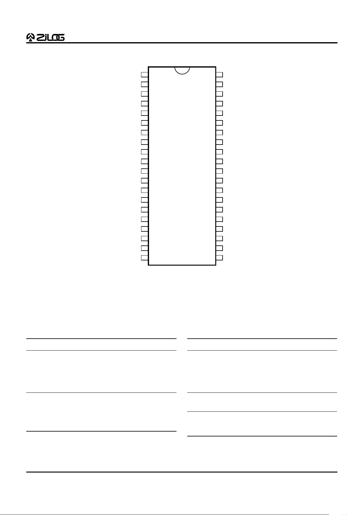
PIN IDENTIFICATION
Figure 2. 40-Pin DIP Pin Configuration
Pin # Symbol Function Direction
1V
CC
Power Supply Input
2 CLK Out Clock Out Output
3 RC In Z8 Clock Input
4 P37 Port 3, Pin 7 Output
5 P30 Port 3, Pin 0 Input
6 /RESET Reset Input
*7 GND Ground
*8 N/C Not Connected
9 /WDTOUT Watch-Dog Timer Output
10 P35 Port 3, Pin 5 Output
Pin # Symbol Function Direction
11 GND Ground
12 P32 Port 3, Pin 2 Input
13-20 P07-P00 Port 0, Pins 0,1,2,3,4,5,6,7 In/Output
21-28 P17-P10 Port 1, Pins 0,1,2,3,4,5,6,7 In/Output
29 P34 Port 3, Pin 4 Output
30 P33 Port 3, Pin 3 Input
31-38 P27-P20 Port 2, Pins 0,1,2,3,4,5,6,7 In/Output
34-38 P24-P20 Port 2, Pins 0, 1, 2, 3, 4 In/Output
39 P31 Port 3, Pin 1 Input
40 P36 Port 3, Pin 6 Output
Table 1. 40-Pin DIP Pin Identification
1
2
3
4
5
6
7
8
9
10
11
12
13
14
15
16
17
18
19
20
VCC
CLK Out
RC In
P37
P30
/RESET
*GND
*N/C
/WDTOUT
P35
GND
P32
P00
P01
P02
P03
P04
P05
P06
P07
P36
P31
P27
P26
P25
P24
P23
P22
P21
P20
P33
P34
P17
P16
P15
P14
P13
P12
P11
P10
40
39
38
37
36
35
34
33
32
31
30
29
28
27
26
25
24
23
22
21
Z08617
DIP
Note:
* Pin 8 is connected to the chip, although used only for testing.
This pin
must
float. Pin 7 is a test pin and
must
be grounded.
Z08617 NMOS Z8
®
8-BIT MCU
KEYBOARD CONTROLLER
4
ABSOLUTE MAXIMUM RATINGS
Symbol Description Min Max Units
V
CC
Supply Voltage* –0.3 +7.0 V
T
STG
Storage Temp –65 +150 C
T
A
Oper Ambient Temp † †
Notes:
* Voltage on all pins with respect to GND.
† See ordering information
Stresses greater than those listed under Absolute
Maximum Ratings may cause permanent damage to
the device. This is a stress rating only; operation of the
device at any condition above those indicated in the
operational sections of these specifications is not
implied. Exposure to absolute maximum rating conditions for extended periods may affect device reliability.
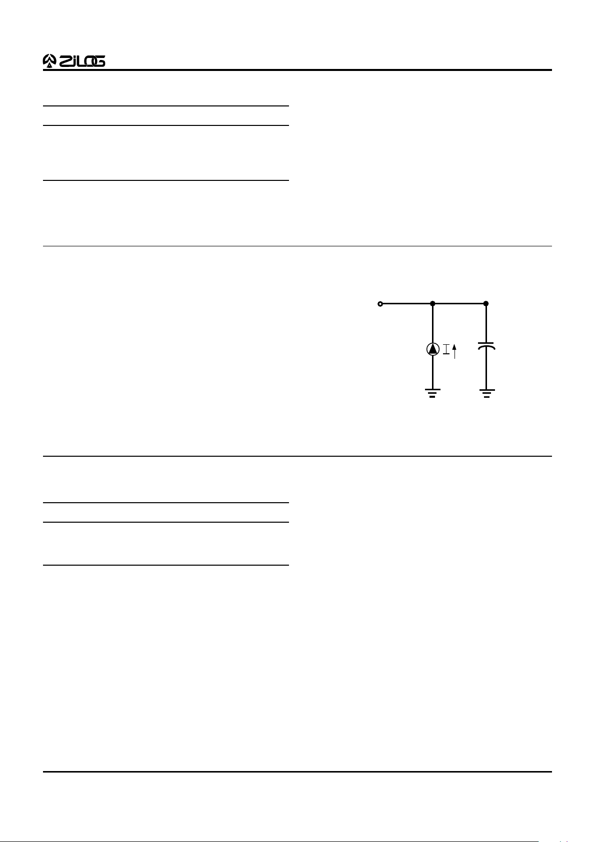
STANDARD TEST CONDITIONS
The characteristics listed here apply for standard test
conditions as noted. All voltages are referenced to
GND. Positive current flows into the referenced pin
(Figure 17).
From Output
Under Test
150 pF
Figure 17. Test Load Diagram
STANDARD TEST CONDITIONS
T
A
= 25°C, VCC = GND = 0V, f = 1.0 MHz, unmeasured pins returned to ground.
Parameter Max
Input capacitance 12 pF
Output capacitance 12 pF
I/O capacitance 12 pF
5
Z08617 NMOS Z8
®
8-BIT MCU
KEYBOARD CONTROLLER
DC CHARACTERISTICS
VCC = 4.75V to 5.25V @ 0°C to -55°C
Sym Parameter Min Max Typ* Unit Condition
V
IH
Input High Voltage 2.0 V
CC
V
V
IL
Input Low Voltage –0.3 0.8 V
V
RH
Reset Input High Voltage 3.8 V
CC
V
V
RL
Reset Input Low Voltage –0.3 0.8 V
V
OH
Output High Voltage 2.0 V IOH = –250 µA (Port 2 only)
Output High Voltage 2.4 V IOH = –250 µA (Port 3 only)
V
OL
Output Low Voltage 0.8 V IOL = 10.0 mA (See note [1] below.)
I
IL
Input Leakage –10 10 µAVIN = 0V, 5.25V (See note [3] below.)
I
OL
Output Leakage –10 10 µAVIN = 0V, 5.25V (See note [2] below.)
I
IR
Reset Input Current –335 –775 –477 µAV
IN
= 0V, 5.25V
I
R1
Input Current –335 –775 µA Pull-up resistor=10.4 Kohms, VIN=0.0V
I
R2
Input Current –1.6 –2.9 mA Pull-up resistor = 2.4 Kohms, VIN=0.0V
I
CC
VCC Supply Current 160 mA
WDT Watch-Dog Timer 2.0 mA VOL=0.4 Volt
Notes:
* Typical @ 25°C
[ 1 ] Ports P37-P34 may be used to sink 12 mA. These may be used
for LEDs or as general-purpose outputs requiring high sink
current.
[ 2 ] P00-P07, P10-P17, P20-P25, P30-P33 as output mode open-
drain as a logic one.
[ 3 ] P00-P07, P10-P17, P20-P25, P30-P33 as output mode open-
drain as a logic one.
Z08617 NMOS Z8
®
8-BIT MCU
KEYBOARD CONTROLLER
6
PIN FUNCTIONS
RCIN This pin is connected between a precision resistor
on the power supply from the precision RC Oscillator.
CLK Out This pin is the syste m clock of the Z8 and
runs at the frequency of the RC Oscillator. Any load on
this pin will effect the RC Oscillator frequency.
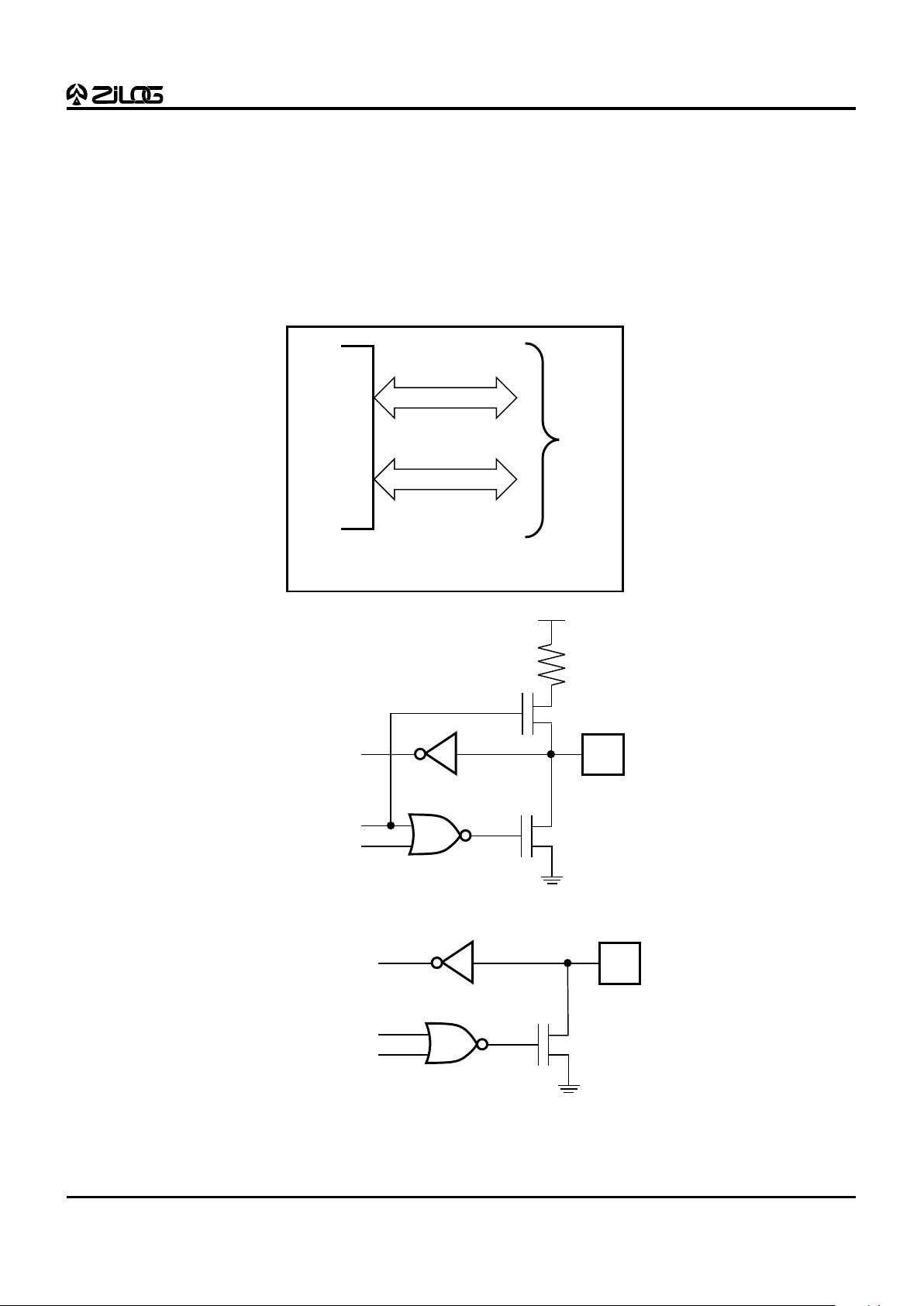
Port 0 (P07-P00). Port 0 is an 8-bit, nibble programmable, bi-directional, NMOS compatible I/O port. These
eight I/O lines can be configured under software
control as a nibble input port, or as a nibble open-drain
output port. When used as an I/O port, inputs are
standard NMOS (Figure 5). Port P03-P00 has 10.4
Kohms (±35%) pull-up resistors when configured as
inputs.
Figure 5. Port 0 Configuration
Port 0
I/O
(Open-Drain Output)
Z8615
4
4
Input
Output
Pad
OEN
10.4 Kohms
(a) Port P00-P03
Input
Output
Pad
OEN
(b) Port P04-P07
7
Z08617 NMOS Z8
®
8-BIT MCU
KEYBOARD CONTROLLER
PIN FUNCTIONS (Continued)
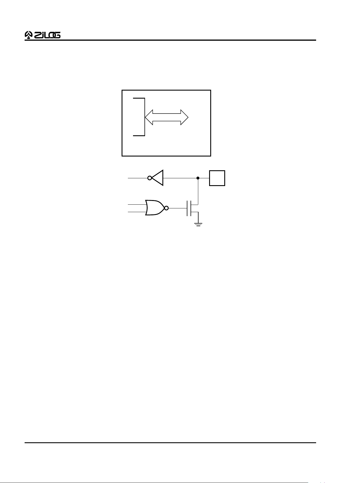
Port 1 (P17-P10). Port 1 is an 8-bit, byte programmable,
bidirectional, NMOS compatible I/O port. These eight I/O
lines are configured under software control program as a
byte input port or as an open-drain output port. When used
as an I/O port, inputs are standard NMOS (Figure 6).
Port 1
I/O
(Open-Drain Output)
Z8615 8
Input
Output
Pad
OEN
Figure 6. Port 1 Configuration
Z08617 NMOS Z8
®
8-BIT MCU
KEYBOARD CONTROLLER
8
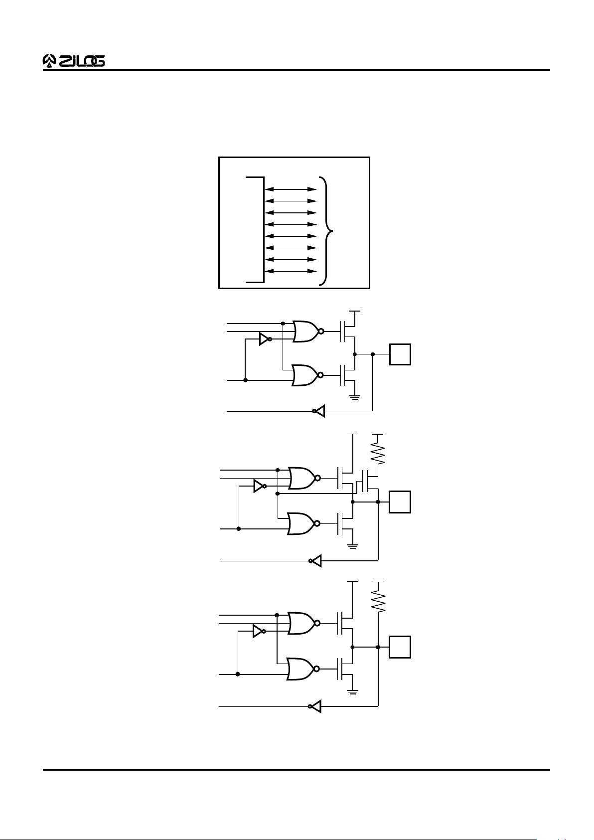
Port 2 (P27-P20). Port 2 is an 8-bit, bit programmable, bidirectional, NMOS compatible I/O port. These eight I/O
lines are configured under the software control program
for I/O. Port 2 can be programmed as bit-by-bit independently, as input or output, or configured to provide open-
drain outputs (Figure 7). P26 and P27 have 2.4 Kohms
(± 25%) pull-up resistors and are capable of sourcing
2.4 mA. P24 and P25 have 10.4 Kohms (± 35%) pull-up
when configured as inputs.
Open-Drain
OUT
OEN
IN
Pad
Input
(a) Ports P20-P23
Port 2
(I/O)
Z8615
Open-Drain
OUT
OEN
IN
Pad
10.4 Kohms
Input
(b) Ports P24-P25
Open-Drain
OUT
OEN
IN
Pad
2.4 Kohms
Input
(c) Ports P26-P27
Figure 7. Port 2 Configuration
 Loading...