

Page 1

eZ80L92
Product Specification
PRELIMINARY
PS013011-0204
ZiLOG Worldwide Headquarters • 532 Race Street • San Jose, CA 95126
Telephone: 408.558.8500 • Fax: 408.558.8300 • www.ZiLOG.com
Page 2

ii
T
©
eZ80L92 Product Specification
This publication is subject to replacement by a later edition. T o determine whether
a later edition exists, or to request copies of publications, contact:
ZiLOG W orldwide Headquarters
532 Race Street
San Jose, CA 95126
elephone: 408.558.8500
Fax: 408.558.8300
www .ZiLOG.com
PS013011-0204
Document Disclaimer
ZiLOG is a registered trademark of ZiLOG Inc. in the United States and in other countries. All other
products and/or service names mentioned herein may be trademarks of the companies with which
they are associated.
2004 by ZiLOG, Inc. All rights reserved. Information in this publication concerning the devices,
applications, or technology described is intended to suggest possible uses and may be superseded.
ZiLOG, INC. DOES NOT ASSUME LIABILITY FOR OR PROVIDE A REPRESENT A TION OF
ACCURACY OF THE INFORMA TION, DEVICES, OR TECHNOLOGY DESCRIBED IN THIS
DOCUMENT . ZiLOG ALSO DOES NOT ASSUME LIABILITY FOR INTELLECTUAL PROPER TY
INFRINGEMENT RELA TED IN ANY MANNER T O USE OF INFORMA TION, DEVICES, OR
TECHNOLOGY DESCRIBED HEREIN OR OTHER WISE. Devices sold by ZiLOG, Inc. are covered
by warranty and limitation of liability provisions appearing in the ZiLOG, Inc. T erms and Conditions of
Sale. ZiLOG, Inc. makes no warranty of merchantability or fitness for any purpose Except with the
express written approval of ZiLOG, use of information, devices, or technology as critical components
of life support systems is not authorized. No licenses are conveyed, implicitly or otherwise, by this
document under any intellectual property rights.
PRELIMINARY
Page 3

able of Contents
ist of Figures . . . . . . . . . . . . . . . . . . . . . . . . . . . . . . . . . . . . . . . . . . . . . . . . . . . vii
List of Tables . . . . . . . . . . . . . . . . . . . . . . . . . . . . . . . . . . . . . . . . . . . . . . . . . . . . ix
Architectural Overview . . . . . . . . . . . . . . . . . . . . . . . . . . . . . . . . . . . . . . . . . . . . 1
Features . . . . . . . . . . . . . . . . . . . . . . . . . . . . . . . . . . . . . . . . . . . . . . . . . . . . 1
Block Diagram . . . . . . . . . . . . . . . . . . . . . . . . . . . . . . . . . . . . . . . . . . . . . . . . 2
Pin Description . . . . . . . . . . . . . . . . . . . . . . . . . . . . . . . . . . . . . . . . . . . . . . . 4
Pin Characteristics . . . . . . . . . . . . . . . . . . . . . . . . . . . . . . . . . . . . . . . . . . . 20
Register Map . . . . . . . . . . . . . . . . . . . . . . . . . . . . . . . . . . . . . . . . . . . . . . . . . . . 25
®
eZ80
PU Core . . . . . . . . . . . . . . . . . . . . . . . . . . . . . . . . . . . . . . . . . . . . . . . . 32
Features . . . . . . . . . . . . . . . . . . . . . . . . . . . . . . . . . . . . . . . . . . . . . . . . . . . 32
New and Improved Instructions . . . . . . . . . . . . . . . . . . . . . . . . . . . . . . . . . . 32
T
L
C
eZ80L92 Product Specification
iii
Reset . . . . . . . . . . . . . . . . . . . . . . . . . . . . . . . . . . . . . . . . . . . . . . . . . . . . . . . . . 34
RESET Operation . . . . . . . . . . . . . . . . . . . . . . . . . . . . . . . . . . . . . . . . . . . . 34
Low-Power Modes . . . . . . . . . . . . . . . . . . . . . . . . . . . . . . . . . . . . . . . . . . . . . . . 35
Overview . . . . . . . . . . . . . . . . . . . . . . . . . . . . . . . . . . . . . . . . . . . . . . . . . . . 35
SLEEP Mode . . . . . . . . . . . . . . . . . . . . . . . . . . . . . . . . . . . . . . . . . . . . . . . . 35
HALT Mode . . . . . . . . . . . . . . . . . . . . . . . . . . . . . . . . . . . . . . . . . . . . . . . . . 36
Clock Peripheral Power-Down Registers . . . . . . . . . . . . . . . . . . . . . . . . . . 36
General-Purpose Input/Output . . . . . . . . . . . . . . . . . . . . . . . . . . . . . . . . . . . . . 39
GPIO Overview . . . . . . . . . . . . . . . . . . . . . . . . . . . . . . . . . . . . . . . . . . . . . . 39
GPIO Operation . . . . . . . . . . . . . . . . . . . . . . . . . . . . . . . . . . . . . . . . . . . . . . 39
GPIO Interrupts . . . . . . . . . . . . . . . . . . . . . . . . . . . . . . . . . . . . . . . . . . . . . . 42
GPIO Control Registers . . . . . . . . . . . . . . . . . . . . . . . . . . . . . . . . . . . . . . . . 43
Interrupt Controller . . . . . . . . . . . . . . . . . . . . . . . . . . . . . . . . . . . . . . . . . . . . . . 45
Maskable Interrupts . . . . . . . . . . . . . . . . . . . . . . . . . . . . . . . . . . . . . . . . . . . 45
Nonmaskable Interrupts . . . . . . . . . . . . . . . . . . . . . . . . . . . . . . . . . . . . . . . 47
Chip Selects and Wait States . . . . . . . . . . . . . . . . . . . . . . . . . . . . . . . . . . . . . . 48
Memory and I/O Chip Selects . . . . . . . . . . . . . . . . . . . . . . . . . . . . . . . . . . . 48
Memory Chip Select Operation . . . . . . . . . . . . . . . . . . . . . . . . . . . . . . . . . . 48
I/O Chip Select Operation . . . . . . . . . . . . . . . . . . . . . . . . . . . . . . . . . . . . . . 50
Wait States . . . . . . . . . . . . . . . . . . . . . . . . . . . . . . . . . . . . . . . . . . . . . . . . . 51
WAIT Input Signal . . . . . . . . . . . . . . . . . . . . . . . . . . . . . . . . . . . . . . . . . . . . 51
Chip Selects During Bus Request/Bus Acknowledge Cycles . . . . . . . . . . . 52
Bus Mode Controller . . . . . . . . . . . . . . . . . . . . . . . . . . . . . . . . . . . . . . . . . . 53
eZ80 Bus Mode . . . . . . . . . . . . . . . . . . . . . . . . . . . . . . . . . . . . . . . . . . . . . . 53
PS013011-0204
PRELIMINARY
Table of Content s
Page 4

eZ80L92 Product Specification
Z80 Bus Mode . . . . . . . . . . . . . . . . . . . . . . . . . . . . . . . . . . . . . . . . . . . . . . . 53
Intel Bus Mode . . . . . . . . . . . . . . . . . . . . . . . . . . . . . . . . . . . . . . . . . . . . . . 55
Motorola Bus Mode . . . . . . . . . . . . . . . . . . . . . . . . . . . . . . . . . . . . . . . . . . . 62
Chip Select Registers . . . . . . . . . . . . . . . . . . . . . . . . . . . . . . . . . . . . . . . . . 66
Watch-Dog Timer . . . . . . . . . . . . . . . . . . . . . . . . . . . . . . . . . . . . . . . . . . . . . . . 71
Watch-Dog Timer Overview . . . . . . . . . . . . . . . . . . . . . . . . . . . . . . . . . . . . 71
Watch-Dog Timer Operation . . . . . . . . . . . . . . . . . . . . . . . . . . . . . . . . . . . . 72
Watch-Dog Timer Registers . . . . . . . . . . . . . . . . . . . . . . . . . . . . . . . . . . . . 73
Programmable Reload Timers . . . . . . . . . . . . . . . . . . . . . . . . . . . . . . . . . . . . . 75
Programmable Reload Timers Overview . . . . . . . . . . . . . . . . . . . . . . . . . . 75
Programmable Reload Timer Operation . . . . . . . . . . . . . . . . . . . . . . . . . . . 76
Programmable Reload Timer Registers . . . . . . . . . . . . . . . . . . . . . . . . . . . 80
Real-Time Clock . . . . . . . . . . . . . . . . . . . . . . . . . . . . . . . . . . . . . . . . . . . . . . . . 86
Real-Time Clock Overview . . . . . . . . . . . . . . . . . . . . . . . . . . . . . . . . . . . . . 86
Real-Time Clock Alarm . . . . . . . . . . . . . . . . . . . . . . . . . . . . . . . . . . . . . . . . 87
Real-Time Clock Oscillator and Source Selection . . . . . . . . . . . . . . . . . . . . 87
Real-Time Clock Battery Backup . . . . . . . . . . . . . . . . . . . . . . . . . . . . . . . . 87
Real-Time Clock Recommended Operation . . . . . . . . . . . . . . . . . . . . . . . . 87
Real-Time Clock Registers . . . . . . . . . . . . . . . . . . . . . . . . . . . . . . . . . . . . . 88
iv
Universal Asynchronous Receiver/Transmitter . . . . . . . . . . . . . . . . . . . . . . . . 102
UART Functional Description . . . . . . . . . . . . . . . . . . . . . . . . . . . . . . . . . . 102
UART Interrupts . . . . . . . . . . . . . . . . . . . . . . . . . . . . . . . . . . . . . . . . . . . . 104
UART Recommended Usage . . . . . . . . . . . . . . . . . . . . . . . . . . . . . . . . . . 105
Baud Rate Generator . . . . . . . . . . . . . . . . . . . . . . . . . . . . . . . . . . . . . . . . 107
BRG Control Registers . . . . . . . . . . . . . . . . . . . . . . . . . . . . . . . . . . . . . . . 107
UART Registers . . . . . . . . . . . . . . . . . . . . . . . . . . . . . . . . . . . . . . . . . . . . 109
Infrared Encoder/Decoder . . . . . . . . . . . . . . . . . . . . . . . . . . . . . . . . . . . . . . . . 120
Functional Description . . . . . . . . . . . . . . . . . . . . . . . . . . . . . . . . . . . . . . . . 120
Transmit . . . . . . . . . . . . . . . . . . . . . . . . . . . . . . . . . . . . . . . . . . . . . . . . . . 121
Receive . . . . . . . . . . . . . . . . . . . . . . . . . . . . . . . . . . . . . . . . . . . . . . . . . . . 121
Jitter . . . . . . . . . . . . . . . . . . . . . . . . . . . . . . . . . . . . . . . . . . . . . . . . . . . . . . 122
Infrared Encoder/Decoder Signal Pins . . . . . . . . . . . . . . . . . . . . . . . . . . . 122
Loopback Testing . . . . . . . . . . . . . . . . . . . . . . . . . . . . . . . . . . . . . . . . . . . 123
Serial Peripheral Interface . . . . . . . . . . . . . . . . . . . . . . . . . . . . . . . . . . . . . . . . 125
SPI Signals . . . . . . . . . . . . . . . . . . . . . . . . . . . . . . . . . . . . . . . . . . . . . . . . 126
SPI Functional Description . . . . . . . . . . . . . . . . . . . . . . . . . . . . . . . . . . . . 128
SPI Flags . . . . . . . . . . . . . . . . . . . . . . . . . . . . . . . . . . . . . . . . . . . . . . . . . . 128
SPI Baud Rate Generator . . . . . . . . . . . . . . . . . . . . . . . . . . . . . . . . . . . . . 129
Data Transfer Procedure with SPI Configured as the Master . . . . . . . . . . 130
PS013011-0204 PRELIMINARY Table of Contents
Page 5

eZ80L92 Product Specification
Data Transfer Procedure with SPI Configured as a Slave . . . . . . . . . . . . 130
SPI Registers . . . . . . . . . . . . . . . . . . . . . . . . . . . . . . . . . . . . . . . . . . . . . . 130
I2C Serial I/O Interface . . . . . . . . . . . . . . . . . . . . . . . . . . . . . . . . . . . . . . . . . . 135
I2C General Characteristics . . . . . . . . . . . . . . . . . . . . . . . . . . . . . . . . . . . . 135
Transferring Data . . . . . . . . . . . . . . . . . . . . . . . . . . . . . . . . . . . . . . . . . . . 137
Clock Synchronization . . . . . . . . . . . . . . . . . . . . . . . . . . . . . . . . . . . . . . . . 138
Operating Modes . . . . . . . . . . . . . . . . . . . . . . . . . . . . . . . . . . . . . . . . . . . . 140
I2C Registers . . . . . . . . . . . . . . . . . . . . . . . . . . . . . . . . . . . . . . . . . . . . . . . 147
ZiLOG Debug Interface . . . . . . . . . . . . . . . . . . . . . . . . . . . . . . . . . . . . . . . . . . 156
Introduction . . . . . . . . . . . . . . . . . . . . . . . . . . . . . . . . . . . . . . . . . . . . . . . . 156
ZDI-Supported Protocol . . . . . . . . . . . . . . . . . . . . . . . . . . . . . . . . . . . . . . . 157
ZDI Clock and Data Conventions . . . . . . . . . . . . . . . . . . . . . . . . . . . . . . . 158
ZDI Start Condition . . . . . . . . . . . . . . . . . . . . . . . . . . . . . . . . . . . . . . . . . . 158
ZDI Register Addressing . . . . . . . . . . . . . . . . . . . . . . . . . . . . . . . . . . . . . . 160
ZDI Write Operations . . . . . . . . . . . . . . . . . . . . . . . . . . . . . . . . . . . . . . . . . 161
ZDI Read Operations . . . . . . . . . . . . . . . . . . . . . . . . . . . . . . . . . . . . . . . . 162
Operation of the eZ80L92 during ZDI BREAKpoints . . . . . . . . . . . . . . . . . 163
Bus Requests During ZDI Debug Mode . . . . . . . . . . . . . . . . . . . . . . . . . . 163
ZDI Write-Only Registers . . . . . . . . . . . . . . . . . . . . . . . . . . . . . . . . . . . . . 164
ZDI Read-Only Registers . . . . . . . . . . . . . . . . . . . . . . . . . . . . . . . . . . . . . 166
ZDI Register Definitions . . . . . . . . . . . . . . . . . . . . . . . . . . . . . . . . . . . . . . 166
v
On-Chip Instrumentation . . . . . . . . . . . . . . . . . . . . . . . . . . . . . . . . . . . . . . . . . 182
Introduction to On-Chip Instrumentation . . . . . . . . . . . . . . . . . . . . . . . . . . 182
OCI Activation . . . . . . . . . . . . . . . . . . . . . . . . . . . . . . . . . . . . . . . . . . . . . . 182
OCI Interface . . . . . . . . . . . . . . . . . . . . . . . . . . . . . . . . . . . . . . . . . . . . . . . 183
OCI Information Requests . . . . . . . . . . . . . . . . . . . . . . . . . . . . . . . . . . . . . 184
eZ80® CPU Instruction Set . . . . . . . . . . . . . . . . . . . . . . . . . . . . . . . . . . . . . . . 185
Op-Code Map . . . . . . . . . . . . . . . . . . . . . . . . . . . . . . . . . . . . . . . . . . . . . . . . . 189
On-Chip Oscillators . . . . . . . . . . . . . . . . . . . . . . . . . . . . . . . . . . . . . . . . . . . . . 196
20 MHz Primary Crystal Oscillator Operation . . . . . . . . . . . . . . . . . . . . . . 196
50 MHz Primary Crystal Oscillator Operation . . . . . . . . . . . . . . . . . . . . . . 197
32 KHz Real-Time Clock Crystal Oscillator Operation . . . . . . . . . . . . . . . 199
Electrical Characteristics . . . . . . . . . . . . . . . . . . . . . . . . . . . . . . . . . . . . . . . . . 201
Absolute Maximum Ratings . . . . . . . . . . . . . . . . . . . . . . . . . . . . . . . . . . . . 201
DC Characteristics . . . . . . . . . . . . . . . . . . . . . . . . . . . . . . . . . . . . . . . . . . . . . 202
AC Characteristics . . . . . . . . . . . . . . . . . . . . . . . . . . . . . . . . . . . . . . . . . . . . . . 204
External Memory Read Timing . . . . . . . . . . . . . . . . . . . . . . . . . . . . . . . . . 204
External Memory Write Timing . . . . . . . . . . . . . . . . . . . . . . . . . . . . . . . . . 206
PS013011-0204 PRELIMINARY Table of Contents
Page 6

eZ80L92 Product Specification
External I/O Read Timing . . . . . . . . . . . . . . . . . . . . . . . . . . . . . . . . . . . . . 208
External I/O Write Timing . . . . . . . . . . . . . . . . . . . . . . . . . . . . . . . . . . . . . 209
Wait State Timing for Read Operations . . . . . . . . . . . . . . . . . . . . . . . . . . . 211
Wait State Timing for Write Operations . . . . . . . . . . . . . . . . . . . . . . . . . . . 212
General Purpose I/O Port Input Sample Timing . . . . . . . . . . . . . . . . . . . . 213
General Purpose I/O Port Output Timing . . . . . . . . . . . . . . . . . . . . . . . . . 213
External Bus Acknowledge Timing . . . . . . . . . . . . . . . . . . . . . . . . . . . . . . 214
External System Clock Driver (PHI) Timing . . . . . . . . . . . . . . . . . . . . . . . 214
Packaging . . . . . . . . . . . . . . . . . . . . . . . . . . . . . . . . . . . . . . . . . . . . . . . . . . . . 215
Ordering Information . . . . . . . . . . . . . . . . . . . . . . . . . . . . . . . . . . . . . . . . . . . . 216
Part Number Description . . . . . . . . . . . . . . . . . . . . . . . . . . . . . . . . . . . . . . 216
Precharacterization Product . . . . . . . . . . . . . . . . . . . . . . . . . . . . . . . . . . . 217
Document Information . . . . . . . . . . . . . . . . . . . . . . . . . . . . . . . . . . . . . . . . . . . 218
Document Number Description . . . . . . . . . . . . . . . . . . . . . . . . . . . . . . . . . 218
Change Log . . . . . . . . . . . . . . . . . . . . . . . . . . . . . . . . . . . . . . . . . . . . . . . . 218
vi
Index . . . . . . . . . . . . . . . . . . . . . . . . . . . . . . . . . . . . . . . . . . . . . . . . . . . . . . . . 219
Customer Feedback Form . . . . . . . . . . . . . . . . . . . . . . . . . . . . . . . . . . . . . . . . 227
PS013011-0204 PRELIMINARY Table of Contents
Page 7

List of Figures
Figure 1. eZ80L92 Block Diagram . . . . . . . . . . . . . . . . . . . . . . . . . . . . . . . . . . 3
Figure 2. 100-Pin LQFP Configuration of the eZ80L92 . . . . . . . . . . . . . . . . . . 4
Figure 3. GPIO Port Pin Block Diagram . . . . . . . . . . . . . . . . . . . . . . . . . . . . . 42
Figure 4. Memory Chip Select Example . . . . . . . . . . . . . . . . . . . . . . . . . . . . . 49
Figure 5. Wait Input Sampling Block Diagram . . . . . . . . . . . . . . . . . . . . . . . . 51
Figure 6. Wait State Operation Example (Read Operation) . . . . . . . . . . . . . . 52
Figure 7. Z80 Bus Mode Read Timing Example . . . . . . . . . . . . . . . . . . . . . . . 54
Figure 8. Z80 Bus Mode Write Timing Example . . . . . . . . . . . . . . . . . . . . . . . 55
Figure 9. IntelTM Bus Mode Signal and Pin Mapping . . . . . . . . . . . . . . . . . . . 56
Figure 10. Intel™ Bus Mode Read Timing Example (Separate Address and
Data Buses) . . . . . . . . . . . . . . . . . . . . . . . . . . . . . . . . . . . . . . . . . . . 58
Figure 11. Intel™ Bus Mode Write Timing Example (Separate Address and
Data Buses) . . . . . . . . . . . . . . . . . . . . . . . . . . . . . . . . . . . . . . . . . . . 59
Figure 12. Intel™ Bus Mode Read Timing Example (Multiplexed Address
and Data Bus) . . . . . . . . . . . . . . . . . . . . . . . . . . . . . . . . . . . . . . . . . 61
Figure 13. IntelTM Bus Mode Write Timing Example (Multiplexed Address
and Data Bus) . . . . . . . . . . . . . . . . . . . . . . . . . . . . . . . . . . . . . . . . . 62
Figure 14. Motorola Bus Mode Signal and Pin Mapping . . . . . . . . . . . . . . . . . 63
Figure 15. Motorola Bus Mode Read Timing Example . . . . . . . . . . . . . . . . . . . 65
Figure 16. Motorola Bus Mode Write Timing Example . . . . . . . . . . . . . . . . . . . 66
Figure 17. Watch-Dog Timer Block Diagram . . . . . . . . . . . . . . . . . . . . . . . . . . 71
Figure 18. Programmable Reload Timer Block Diagram . . . . . . . . . . . . . . . . . 75
Figure 19. PRT Single Pass Mode Operation Example . . . . . . . . . . . . . . . . . . 77
Figure 20. PRT Continuous Mode Operation Example . . . . . . . . . . . . . . . . . . 78
Figure 21. PRT Timer Output Operation Example . . . . . . . . . . . . . . . . . . . . . . 80
Figure 22. Real-Time Clock and 32KHz Oscillator Block Diagram . . . . . . . . . . 86
Figure 23. UART Block Diagram . . . . . . . . . . . . . . . . . . . . . . . . . . . . . . . . . . . 102
Figure 24. Infrared System Block Diagram . . . . . . . . . . . . . . . . . . . . . . . . . . . 120
Figure 25. Infrared Data Transmission . . . . . . . . . . . . . . . . . . . . . . . . . . . . . . 121
Figure 26. Infrared Data Reception . . . . . . . . . . . . . . . . . . . . . . . . . . . . . . . . 122
Figure 27. SPI Master Device . . . . . . . . . . . . . . . . . . . . . . . . . . . . . . . . . . . . . 125
Figure 28. SPI Slave Device . . . . . . . . . . . . . . . . . . . . . . . . . . . . . . . . . . . . . . 125
Figure 29. SPI Timing . . . . . . . . . . . . . . . . . . . . . . . . . . . . . . . . . . . . . . . . . . . 127
Figure 30. I2C Clock and Data Relationship . . . . . . . . . . . . . . . . . . . . . . . . . . 136
Figure 31. START and STOP Conditions In I2C Protocol . . . . . . . . . . . . . . . . 136
Figure 32. I2C Frame Structure . . . . . . . . . . . . . . . . . . . . . . . . . . . . . . . . . . . . 137
eZ80L92 Product Specification
vii
PS013011-0204 PRELIMINARY List of Figures
Page 8

eZ80L92 Product Specification
Figure 33. I2C Acknowledge . . . . . . . . . . . . . . . . . . . . . . . . . . . . . . . . . . . . . . 138
Figure 34. Clock Synchronization In I2C Protocol . . . . . . . . . . . . . . . . . . . . . . 139
Figure 35. Typical ZDI Debug Setup . . . . . . . . . . . . . . . . . . . . . . . . . . . . . . . . 156
Figure 36. Schematic For Building a Target Board ZPAK II Connector . . . . . 157
Figure 37. ZDI Write Timing . . . . . . . . . . . . . . . . . . . . . . . . . . . . . . . . . . . . . . 159
Figure 38. ZDI Read Timing . . . . . . . . . . . . . . . . . . . . . . . . . . . . . . . . . . . . . . 159
Figure 39. ZDI Address Write Timing . . . . . . . . . . . . . . . . . . . . . . . . . . . . . . . 160
Figure 40. ZDI Single-Byte Data Write Timing . . . . . . . . . . . . . . . . . . . . . . . . 161
Figure 41. ZDI Block Data Write Timing . . . . . . . . . . . . . . . . . . . . . . . . . . . . . 162
Figure 42. ZDI Single-Byte Data Read Timing . . . . . . . . . . . . . . . . . . . . . . . . 162
Figure 43. ZDI Block Data Read Timing . . . . . . . . . . . . . . . . . . . . . . . . . . . . . 163
Figure 44. Recommended Crystal Oscillator Configuration
(20MHz operation) . . . . . . . . . . . . . . . . . . . . . . . . . . . . . . . . . . . . . 196
Figure 45. Recommended Crystal Oscillator Configuration
(50MHz operation) . . . . . . . . . . . . . . . . . . . . . . . . . . . . . . . . . . . . . 198
Figure 46. Recommended Crystal Oscillator Configuration
(32KHz operation) . . . . . . . . . . . . . . . . . . . . . . . . . . . . . . . . . . . . . 199
Figure 47. ICC vs. Frequency (Typical @ 3.3 V, 25ºC) . . . . . . . . . . . . . . . . . . 203
Figure 48. ICC vs. WAIT (Typical @ 3.3 V, 25ºC) . . . . . . . . . . . . . . . . . . . . . . 203
Figure 49. External Memory Read Timing . . . . . . . . . . . . . . . . . . . . . . . . . . . 205
Figure 50. External Memory Write Timing . . . . . . . . . . . . . . . . . . . . . . . . . . . 206
Figure 51. External I/O Read Timing . . . . . . . . . . . . . . . . . . . . . . . . . . . . . . . 208
Figure 52. External I/O Write Timing . . . . . . . . . . . . . . . . . . . . . . . . . . . . . . . . 209
Figure 53. Wait State Timing for Read Operations . . . . . . . . . . . . . . . . . . . . . 211
Figure 54. Wait State Timing for Write Operations . . . . . . . . . . . . . . . . . . . . . 212
Figure 55. Port Input Sample Timing . . . . . . . . . . . . . . . . . . . . . . . . . . . . . . . 213
Figure 56. GPIO Port Output Timing . . . . . . . . . . . . . . . . . . . . . . . . . . . . . . . . 213
Figure 57. 100-Lead Plastic Low-Profile Quad Flat Package (LQFP) . . . . . . 215
viii
PS013011-0204 PRELIMINARY List of Figures
Page 9

List of Tables
Table 1. 100-Pin LQFP Pin Identification of the eZ80L92 Device . . . . . . . . . . . . 5
Table 2. Pin Characteristics of the eZ80L92 . . . . . . . . . . . . . . . . . . . . . . . . . . . 20
Table 3. Register Map . . . . . . . . . . . . . . . . . . . . . . . . . . . . . . . . . . . . . . . . . . . . 25
Table 4. Clock Peripheral Power-Down Register 1 . . . . . . . . . . . . . . . . . . . . . . 37
Table 5. Clock Peripheral Power-Down Register 2 . . . . . . . . . . . . . . . . . . . . . . 38
Table 6. GPIO Mode Selection. . . . . . . . . . . . . . . . . . . . . . . . . . . . . . . . . . . . . . 40
Table 7. Port x Data Registers . . . . . . . . . . . . . . . . . . . . . . . . . . . . . . . . . . . . . . 43
Table 8. Port x Data Direction Registers . . . . . . . . . . . . . . . . . . . . . . . . . . . . . . 44
Table 9. Port x Alternate Registers 1 . . . . . . . . . . . . . . . . . . . . . . . . . . . . . . . . . 44
Table 10. Port x Alternate Registers 2 . . . . . . . . . . . . . . . . . . . . . . . . . . . . . . . . 44
Table 11. Interrupt Vector Sources by Priority . . . . . . . . . . . . . . . . . . . . . . . . . . 45
Table 12. Vectored Interrupt Operation . . . . . . . . . . . . . . . . . . . . . . . . . . . . . . . 46
Table 13. Register Values for Memory Chip Select Example . . . . . . . . . . . . . . 50
Table 14. Z80 Bus Mode Read States . . . . . . . . . . . . . . . . . . . . . . . . . . . . . . . . 53
Table 15. Z80 Bus Mode Write States . . . . . . . . . . . . . . . . . . . . . . . . . . . . . . . . 54
Table 16. Intel™ Bus Mode Read States (Separate Address and Data Buses) 56
Table 17. Intel™ Bus Mode Write States (Separate Address and Data Buses) 57
Table 18. Intel™ Bus Mode Write States (Multiplexed Address and Data Bus). 60
Table 19. Intel™ Bus Mode Read States (Multiplexed Address and Data Bus) 60
Table 20. Motorola Bus Mode Read States . . . . . . . . . . . . . . . . . . . . . . . . . . . . 63
Table 21. Motorola Bus Mode Write States . . . . . . . . . . . . . . . . . . . . . . . . . . . . 64
Table 22. Chip Select x Lower Bound Registers . . . . . . . . . . . . . . . . . . . . . . . . 67
Table 23. Chip Select x Upper Bound Registers . . . . . . . . . . . . . . . . . . . . . . . . 67
Table 24. Chip Select x Control Registers . . . . . . . . . . . . . . . . . . . . . . . . . . . . . 68
Table 25. Chip Select x Bus Mode Control Registers . . . . . . . . . . . . . . . . . . . . 69
Table 26. Watch-Dog Timer Approximate Time-Out Delays . . . . . . . . . . . . . . . 72
Table 27. Watch-Dog Timer Control Register . . . . . . . . . . . . . . . . . . . . . . . . . . 73
Table 28. Watch-Dog Timer Reset Register . . . . . . . . . . . . . . . . . . . . . . . . . . . 74
Table 29. PRT Single Pass Mode Operation Example . . . . . . . . . . . . . . . . . . . 77
Table 30. PRT Continuous Mode Operation Example . . . . . . . . . . . . . . . . . . . . 78
Table 31. PRT Timer Out Operation Example . . . . . . . . . . . . . . . . . . . . . . . . . . 80
Table 32. Timer Control Registers . . . . . . . . . . . . . . . . . . . . . . . . . . . . . . . . . . . 81
Table 33. Timer Data Registers—Low Byte . . . . . . . . . . . . . . . . . . . . . . . . . . . . 82
Table 34. Timer Data Registers—High Byte . . . . . . . . . . . . . . . . . . . . . . . . . . . 83
Table 35. Timer Reload Registers—Low Byte . . . . . . . . . . . . . . . . . . . . . . . . . . 83
eZ80L92 Product Specification
ix
PS013011-0204 PRELIMINARY List of Tables
Page 10

eZ80L92 Product Specification
Table 36. Timer Reload Registers—High Byte . . . . . . . . . . . . . . . . . . . . . . . . . 84
Table 37. Timer Input Source Select Register . . . . . . . . . . . . . . . . . . . . . . . . . . 84
Table 38. Real-Time Clock Seconds Register . . . . . . . . . . . . . . . . . . . . . . . . . . 88
Table 39. Real-Time Clock Minutes Register. . . . . . . . . . . . . . . . . . . . . . . . . . . 89
Table 40. Real-Time Clock Hours Register . . . . . . . . . . . . . . . . . . . . . . . . . . . . 90
Table 41. Real-Time Clock Day-of-the-Week Register . . . . . . . . . . . . . . . . . . . 91
Table 42. Real-Time Clock Day-of-the-Month Register . . . . . . . . . . . . . . . . . . . 92
Table 43. Real-Time Clock Month Register . . . . . . . . . . . . . . . . . . . . . . . . . . . . 93
Table 44. Real-Time Clock Year Register . . . . . . . . . . . . . . . . . . . . . . . . . . . . . 94
Table 45. Real-Time Clock Century Register. . . . . . . . . . . . . . . . . . . . . . . . . . . 95
Table 46. Real-Time Clock Alarm Seconds Register . . . . . . . . . . . . . . . . . . . . . 96
Table 47. Real-Time Clock Alarm Minutes Register . . . . . . . . . . . . . . . . . . . . . 97
Table 48. Real-Time Clock Alarm Hours Register . . . . . . . . . . . . . . . . . . . . . . . 98
Table 49. Real-Time Clock Alarm Day-of-the-Week Register . . . . . . . . . . . . . . 99
Table 50. Real-Time Clock Alarm Control Register . . . . . . . . . . . . . . . . . . . . . 100
Table 51. Real-Time Clock Control Register . . . . . . . . . . . . . . . . . . . . . . . . . . 101
Table 52. UART Baud Rate Generator Registers—Low Byte . . . . . . . . . . . . . 108
Table 53. UART Baud Rate Generator Registers—High Byte . . . . . . . . . . . . . 108
Table 54. UART Transmit Holding Registers . . . . . . . . . . . . . . . . . . . . . . . . . . 109
Table 55. UART Receive Buffer Registers. . . . . . . . . . . . . . . . . . . . . . . . . . . . 110
Table 56. UART Interrupt Enable Registers. . . . . . . . . . . . . . . . . . . . . . . . . . . 110
Table 57. UART Interrupt Identification Registers . . . . . . . . . . . . . . . . . . . . . . 111
Table 58. UART Interrupt Status Codes. . . . . . . . . . . . . . . . . . . . . . . . . . . . . . 112
Table 59. UART FIFO Control Registers . . . . . . . . . . . . . . . . . . . . . . . . . . . . . 112
Table 60. UART Line Control Registers . . . . . . . . . . . . . . . . . . . . . . . . . . . . . . 113
Table 61. UART Character Parameter Definition . . . . . . . . . . . . . . . . . . . . . . . 114
Table 62. UART Modem Control Registers . . . . . . . . . . . . . . . . . . . . . . . . . . . 115
Table 63. UART Line Status Registers . . . . . . . . . . . . . . . . . . . . . . . . . . . . . . 116
Table 64. UART Modem Status Registers . . . . . . . . . . . . . . . . . . . . . . . . . . . . 118
Table 65. UART Scratch Pad Registers. . . . . . . . . . . . . . . . . . . . . . . . . . . . . . 119
Table 66. GPIO Mode Selection when using the IrDA Encoder/Decoder . . . . 123
Table 67. Infrared Encoder/Decoder Control Register . . . . . . . . . . . . . . . . . . . 124
Table 68. SPI Clock Phase (CPHA) and Clock Polarity Operation . . . . . . . . . 127
Table 69. SPI Baud Rate Generator Register—High Byte. . . . . . . . . . . . . . . . 131
Table 70. SPI Baud Rate Generator Register—Low Byte . . . . . . . . . . . . . . . . 131
Table 71. SPI Control Register. . . . . . . . . . . . . . . . . . . . . . . . . . . . . . . . . . . . . 132
Table 72. SPI Status Register . . . . . . . . . . . . . . . . . . . . . . . . . . . . . . . . . . . . . 133
Table 73. SPI Receive Buffer Register. . . . . . . . . . . . . . . . . . . . . . . . . . . . . . . 134
x
PS013011-0204 PRELIMINARY List of Tables
Page 11

eZ80L92 Product Specification
Table 74. SPI Transmit Shift Register . . . . . . . . . . . . . . . . . . . . . . . . . . . . . . . 134
Table 75. I2C Master Transmit Status Codes. . . . . . . . . . . . . . . . . . . . . . . . . . 141
Table 76. I2C 10-Bit Master Transmit Status Codes . . . . . . . . . . . . . . . . . . . . 142
Table 77. I2C Master Transmit Status Codes For Data Bytes . . . . . . . . . . . . . 143
Table 78. I2C Master Receive Status Codes . . . . . . . . . . . . . . . . . . . . . . . . . . 144
Table 79. I2C Master Receive Status Codes For Data Bytes. . . . . . . . . . . . . . 145
Table 80. I2C Register Descriptions . . . . . . . . . . . . . . . . . . . . . . . . . . . . . . . . . 147
Table 81. I2C Slave Address Register . . . . . . . . . . . . . . . . . . . . . . . . . . . . . . . 148
Table 82. I2C Extended Slave Address Register . . . . . . . . . . . . . . . . . . . . . . . 149
Table 83. I2C Data Register . . . . . . . . . . . . . . . . . . . . . . . . . . . . . . . . . . . . . . . 149
Table 84. I2C Control Registers . . . . . . . . . . . . . . . . . . . . . . . . . . . . . . . . . . . . 151
Table 85. I2C Status Registers. . . . . . . . . . . . . . . . . . . . . . . . . . . . . . . . . . . . . 152
Table 86. I2C Status Codes . . . . . . . . . . . . . . . . . . . . . . . . . . . . . . . . . . . . . . . 152
Table 87. I2C Clock Control Registers . . . . . . . . . . . . . . . . . . . . . . . . . . . . . . . 154
Table 88. I2C Software Reset Register . . . . . . . . . . . . . . . . . . . . . . . . . . . . . . 155
Table 89. Recommended ZDI Clock vs. System Clock Frequency . . . . . . . . . 157
Table 90. ZDI Write-Only Registers . . . . . . . . . . . . . . . . . . . . . . . . . . . . . . . . . 164
Table 91. ZDI Read-Only Registers . . . . . . . . . . . . . . . . . . . . . . . . . . . . . . . . . 166
Table 92. ZDI Address Match Registers . . . . . . . . . . . . . . . . . . . . . . . . . . . . . 167
Table 93. ZDI BREAK Control Register . . . . . . . . . . . . . . . . . . . . . . . . . . . . . . 168
Table 94. ZDI Master Control Register. . . . . . . . . . . . . . . . . . . . . . . . . . . . . . . 170
Table 95. ZDI Write Data Registers . . . . . . . . . . . . . . . . . . . . . . . . . . . . . . . . . 171
Table 96. ZDI Read/Write Control Register Functions . . . . . . . . . . . . . . . . . . . 172
Table 97. ZDI Bus Control Register . . . . . . . . . . . . . . . . . . . . . . . . . . . . . . . . . 173
Table 98. Instruction Store 4:0 Registers . . . . . . . . . . . . . . . . . . . . . . . . . . . . . 175
Table 99. ZDI Write Memory Register . . . . . . . . . . . . . . . . . . . . . . . . . . . . . . . 176
Table 100. eZ80® Product ID Low Byte Register. . . . . . . . . . . . . . . . . . . . . . . 176
Table 101. eZ80® Product ID Revision Register . . . . . . . . . . . . . . . . . . . . . . . 177
Table 102. eZ80® Product ID High Byte Register . . . . . . . . . . . . . . . . . . . . . . 177
Table 103. ZDI Status Register . . . . . . . . . . . . . . . . . . . . . . . . . . . . . . . . . . . . 178
Table 104. ZDI Read Registers—Low, High and Upper . . . . . . . . . . . . . . . . . 179
Table 105. ZDI Bus Control Register . . . . . . . . . . . . . . . . . . . . . . . . . . . . . . . . 180
Table 106. ZDI Read Memory Register . . . . . . . . . . . . . . . . . . . . . . . . . . . . . . 181
Table 107. OCI Pins . . . . . . . . . . . . . . . . . . . . . . . . . . . . . . . . . . . . . . . . . . . . 183
Table 108. Arithmetic Instructions . . . . . . . . . . . . . . . . . . . . . . . . . . . . . . . . . . 185
Table 109. Bit Manipulation Instructions . . . . . . . . . . . . . . . . . . . . . . . . . . . . . 185
Table 110. Block Transfer and Compare Instructions . . . . . . . . . . . . . . . . . . . 185
Table 111. Exchange Instructions . . . . . . . . . . . . . . . . . . . . . . . . . . . . . . . . . . 186
xi
PS013011-0204 PRELIMINARY List of Tables
Page 12

eZ80L92 Product Specification
Table 112. Input/Output Instructions . . . . . . . . . . . . . . . . . . . . . . . . . . . . . . . . 186
Table 113. Load Instructions . . . . . . . . . . . . . . . . . . . . . . . . . . . . . . . . . . . . . . 187
Table 114. Logical Instructions. . . . . . . . . . . . . . . . . . . . . . . . . . . . . . . . . . . . . 187
Table 115. Processor Control Instructions . . . . . . . . . . . . . . . . . . . . . . . . . . . . 187
Table 116. Program Control Instructions . . . . . . . . . . . . . . . . . . . . . . . . . . . . . 188
Table 117. Rotate and Shift Instructions . . . . . . . . . . . . . . . . . . . . . . . . . . . . . 188
Table 118. Op Code Map—First Op Code . . . . . . . . . . . . . . . . . . . . . . . . . . . . 189
Table 119. Op Code Map—Second Op Code after 0CBh . . . . . . . . . . . . . . . . 190
Table 120. Op Code Map—Second Op Code After 0DDh . . . . . . . . . . . . . . . . 191
Table 121. Op Code Map—Second Op Code After 0EDh . . . . . . . . . . . . . . . . 192
Table 122. Op Code Map—Second Op Code After 0FDh . . . . . . . . . . . . . . . . 193
Table 123. Op Code Map—Fourth Byte After 0DDh, 0CBh, and dd . . . . . . . . 194
Table 124. Op Code Map—Fourth Byte After 0FDh, 0CBh, and dd* . . . . . . . . 195
Table 125. Recommended Crystal Oscillator Specifications
(20 MHz Operation). . . . . . . . . . . . . . . . . . . . . . . . . . . . . . . . . . . . . 197
Table 126. Recommended Crystal Oscillator Specifications
(50MHz Operation) . . . . . . . . . . . . . . . . . . . . . . . . . . . . . . . . . . . . . 198
Table 127. Recommended Crystal Oscillator Specifications
(32 KHz Operation) . . . . . . . . . . . . . . . . . . . . . . . . . . . . . . . . . . . . . 199
Table 128. Absolute Maximum Ratings . . . . . . . . . . . . . . . . . . . . . . . . . . . . . . 201
Table 129. DC Characteristics . . . . . . . . . . . . . . . . . . . . . . . . . . . . . . . . . . . . . 202
Table 130. AC Characteristics . . . . . . . . . . . . . . . . . . . . . . . . . . . . . . . . . . . . . 204
Table 131. External Read Timing. . . . . . . . . . . . . . . . . . . . . . . . . . . . . . . . . . . 205
Table 132. External Write Timing . . . . . . . . . . . . . . . . . . . . . . . . . . . . . . . . . . . 207
Table 133. External I/O Read Timing . . . . . . . . . . . . . . . . . . . . . . . . . . . . . . . . 208
Table 134. External I/O Write Timing . . . . . . . . . . . . . . . . . . . . . . . . . . . . . . . . 210
Table 135. GPIO Port Output Timing . . . . . . . . . . . . . . . . . . . . . . . . . . . . . . . . 214
Table 136. Bus Acknowledge Timing . . . . . . . . . . . . . . . . . . . . . . . . . . . . . . . . 214
Table 137. PHI System Clock Timing. . . . . . . . . . . . . . . . . . . . . . . . . . . . . . . . 214
Table 138. Ordering Information . . . . . . . . . . . . . . . . . . . . . . . . . . . . . . . . . . . 216
xii
PS013011-0204 PRELIMINARY List of Tables
Page 13

Architectural Overview
The eZ80L92 microprocessor is a high-speed single-cycle instruction-fetch microprocessor with a maximum clock speed of 50 MHz. The eZ80L92 is a member of
ZiLOG’s new eZ80® product family. It can operate in Z80-compatible addressing
mode (64 KB) or full 24-bit addressing mode (16 MB). The rich peripheral set of the
eZ80L92 makes it suitable for a variety of applications including industrial control,
embedded communication, and point-of-sale terminals.
Features
• Single-cycle instruction fetch, high-performance, pipelined eZ80® CPU core
• Low power features including SLEEP mode, HALT mode, and selective
peripheral power-down control
eZ80L92 Product Specification
1
1
• Two UARTs with independent baud rate generators
• SPI with independent clock rate generator
• I2C with independent clock rate generator
• Infrared Data Association (IrDA)-compliant infrared encoder/decoder
• New DMA-like eZ80® instructions for efficient block data transfer
• Glueless external peripheral interface with 4 Chip Selects, individual Wait
State generators, and an external WAIT input pin—supports Intel-and Motorola-style buses
• Fixed-priority vectored interrupts (both internal and external) and interrupt
controller
• Real-time clock with on-chip 32 KHz oscillator, selectable 50/60Hz input, and
separate VDD pin for battery backup
• Six 16-bit Counter/Timers with prescalers and direct input/output drive
• Watch-Dog Timer
• 24 bits of General-Purpose I/O
• JTAG and ZDI debug interfaces
• 100-pin LQFP package
• 3.0–3.6 V supply voltage with 5 V tolerant inputs
1. For simplicity, the term eZ80® CPU is referred to as CPU for the bulk of this document.
PS013011-0204 PRELIMINARY Architectural Overview
Page 14

• Operating Temperature Range
–
Standard: 0ºC to +70ºC
–
Extended: –40ºC to +105ºC
eZ80L92 Product Specification
2
Note:
All signals with an overline are active Low. For example, B/W, for which
WORD is active Low, and B/W, for which BYTE is active Low.
Power connections follow these conventional descriptions:
Connection Circuit Device
Power V
Ground GND V
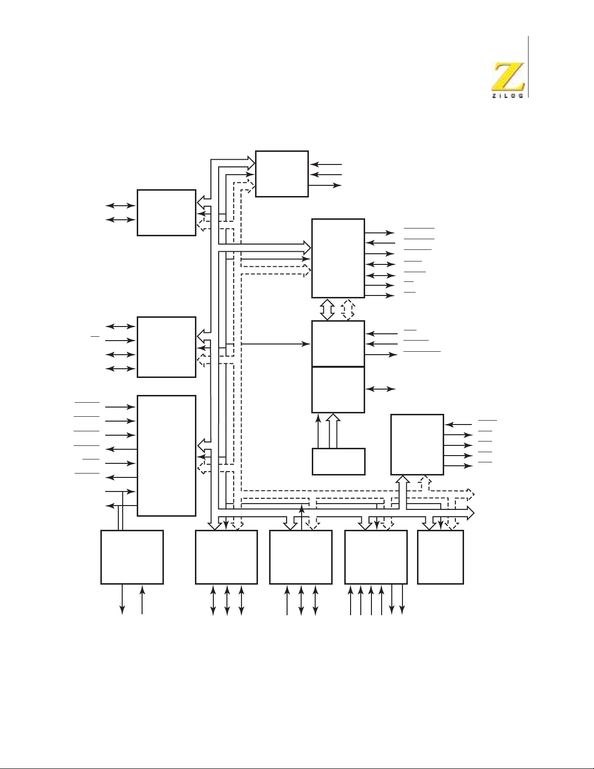
Block Diagram
Figure 1 illustrates a block diagram of the eZ80L92 microprocessor.
CC
V
DD
SS
PS013011-0204 PRELIMINARY Architectural Overview
Page 15
eZ80L92 Product Specification
3
SCL
SDA
SCK
SS
MISO
MOSI
CTS0/1
CD0/1
DSR0/1
DTR0/1
RI0/1
RTS0/1
RxD0/1
TxD0/1
2
I C
Serial
Interface
Serial
Peripheral
Interface
(SPI)
Universal
Asynchronous
Receiver/
Transmitter
(UART)
Real-Time
Clock and
32 KHz
Oscillator
RTC_V
RTC_X
RTC_X
Bus
Controller
eZ80
CPU
ZiLOG
Debug
Interface
(JTAG/ZDI)
Interrupt
Vector
[7:0]
Interrupt
Controller
DD
IN
OUT
BUSACK
BUSREQ
INSTRD
IORQ
MREQ
RD
WR
NMI
RESET
HALT_SLP
JTAG/ZDI Signals (5)
Chip
Select
and
Wait State
Generator
WAIT
CS0
CS1
CS2
CS3
DATA[7:0]
ADDR[23:0]
IrDA
Encoder/
Decoder
IR_TxD
IR_RxD
8-Bit
General
Purpose
I/O Port
(GPIO)
PB[7:0]
PC[7:0]
PD[7:0]
Crystal
Oscillator
and
System Clock
Generator
IN
X
OUT
X
PHI
Programmable
Reload
Timer/Counters
(6)
T0_IN
T1_IN
T2_IN
T3_IN
T4_OUT
T5_OUT
Watch-Dog
Timer
(WDT)
Figure 1. eZ80L92 Block Diagram
PS013011-0204 PRELIMINARY Architectural Overview
Page 16

Pin Description
Figure 2 illustrates the pin layout of the eZ80L92 in the 100-pin LQFP package.
Table 1 describes the pins and their functions.
eZ80L92 Product Specification
4
ADDR0
ADDR1
ADDR2
ADDR3
ADDR4
ADDR5
V
DD
V
SS
ADDR6
ADDR7
ADDR8
ADDR9
ADDR10
ADDR11
ADDR12
ADDR13
ADDR14
V
DD
V
SS
ADDR15
ADDR16
ADDR17
ADDR18
ADDR19
ADDR20
1
2
3
4
5
6
7
8
9
10
11
12
13
14
15
16
17
18
19
20
21
22
23
24
25
PHI
SCL
99
100
262728
ADDR21
ADDR22
ADDR23
DD
SDA
VSSPB7/MOSI
V
95
96
97
98
PB6/MISO
PB5/T5_OUT
PB4/T4_OUT
92
93
94
PB3/SCK
PB2/SS
PB1/T1_IN
90
91
89
OUTXINVSS
PB0/T0_IN
VDDX
86
87
88
85
84
PC7/RI1
83
PC6/DCD1
PC5/DSR1
81
82
PC4/DTR1
PC3/CTS1
79
80
100-Pin LQFP
30
313233343536373839
29
SS
DD
V
CS2
CS3
V
CS0
CS1
DATA0
DATA1
DATA2
4050414243444546474849
SS
DD
V
V
DATA3
DATA4
DATA5
DATA6
DATA7
IORQ
RD
MREQ
Figure 2. 100-Pin LQFP Configuration of the eZ80L92
PC2//RTS1
PC1/RxD1
77
78
WR
INSTRD
PC0/TxD1
76
75
PD7/RI0
74
PD6/DCD0
73
PD5/DSR0
72
PD4/DTR0
71
PD3/CTS0
70
PD2/RTS0
69
PD1/RxD0/IR_RXD
68
PD0/TxD0/IR_TXD
67
V
DD
66
TDO
65
TDI
64
TRIGOUT
63
TCK
62
TMS
61
V
SS
60
RTC_V
59
RTC_XOUT
58
RTC_XIN
57
V
SS
56
V
DD
55
HALT_SLP
54
BUSACK
53
BUSREQ
52
NMI
51
RESET
WAIT
DD
PS013011-0204 PRELIMINARY Architectural Overview
Page 17

eZ80L92 Product Specification
Table 1. 100-Pin LQFP Pin Identification of the eZ80L92 Device
Pin # Symbol Function Signal Direction Description
1 ADDR0 Address Bus Bidirectional Configured as an output in normal opera-
tion. The address bus selects a location in
memory or I/O space to be read or written.
Configured as an input during bus
acknowledge cycles. Drives the Chip
Select/Wait State Generator block to generate Chip Selects.
2 ADDR1 Address Bus Bidirectional Configured as an output in normal opera-
tion. The address bus selects a location in
memory or I/O space to be read or written.
Configured as an input during bus
acknowledge cycles. Drives the Chip
Select/Wait State Generator block to generate Chip Selects.
5
3 ADDR2 Address Bus Bidirectional Configured as an output in normal opera-
tion. The address bus selects a location in
memory or I/O space to be read or written.
Configured as an input during bus
acknowledge cycles. Drives the Chip
Select/Wait State Generator block to generate Chip Selects.
4 ADDR3 Address Bus Bidirectional Configured as an output in normal opera-
tion. The address bus selects a location in
memory or I/O space to be read or written.
Configured as an input during bus
acknowledge cycles. Drives the Chip
Select/Wait State Generator block to generate Chip Selects.
5 ADDR4 Address Bus Bidirectional Configured as an output in normal opera-
tion. The address bus selects a location in
memory or I/O space to be read or written.
Configured as an input during bus
acknowledge cycles. Drives the Chip
Select/Wait State Generator block to generate Chip Selects.
6 ADDR5 Address Bus Bidirectional Configured as an output in normal opera-
tion. The address bus selects a location in
memory or I/O space to be read or written.
Configured as an input during bus
acknowledge cycles. Drives the Chip
Select/Wait State Generator block to generate Chip Selects.
PS013011-0204 PRELIMINARY Architectural Overview
Page 18

eZ80L92 Product Specification
Table 1. 100-Pin LQFP Pin Identification of the eZ80L92 Device (Continued)
Pin # Symbol Function Signal Direction Description
6
7 V
8 V
DD
SS
Power Supply Power Supply.
Ground Ground.
9 ADDR6 Address Bus Bidirectional Configured as an output in normal opera-
tion. The address bus selects a location in
memory or I/O space to be read or written.
Configured as an input during bus
acknowledge cycles. Drives the Chip
Select/Wait State Generator block to generate Chip Selects.
10 ADDR7 Address Bus Bidirectional Configured as an output in normal opera-
tion. The address bus selects a location in
memory or I/O space to be read or written.
Configured as an input during bus
acknowledge cycles. Drives the Chip
Select/Wait State Generator block to generate Chip Selects.
11 ADDR8 Address Bus Bidirectional Configured as an output in normal opera-
tion. The address bus selects a location in
memory or I/O space to be read or written.
Configured as an input during bus
acknowledge cycles. Drives the Chip
Select/Wait State Generator block to generate Chip Selects.
12 ADDR9 Address Bus Bidirectional Configured as an output in normal opera-
tion. The address bus selects a location in
memory or I/O space to be read or written.
Configured as an input during bus
acknowledge cycles. Drives the Chip
Select/Wait State Generator block to generate Chip Selects.
13 ADDR10 Address Bus Bidirectional Configured as an output in normal opera-
tion. The address bus selects a location in
memory or I/O space to be read or written.
Configured as an input during bus
acknowledge cycles. Drives the Chip
Select/Wait State Generator block to generate Chip Selects.
PS013011-0204 PRELIMINARY Architectural Overview
Page 19

eZ80L92 Product Specification
Table 1. 100-Pin LQFP Pin Identification of the eZ80L92 Device (Continued)
Pin # Symbol Function Signal Direction Description
14 ADDR11 Address Bus Bidirectional Configured as an output in normal opera-
tion. The address bus selects a location in
memory or I/O space to be read or written.
Configured as an input during bus
acknowledge cycles. Drives the Chip
Select/Wait State Generator block to generate Chip Selects.
15 ADDR12 Address Bus Bidirectional Configured as an output in normal opera-
tion. The address bus selects a location in
memory or I/O space to be read or written.
Configured as an input during bus
acknowledge cycles. Drives the Chip
Select/Wait State Generator block to generate Chip Selects.
7
16 ADDR13 Address Bus Bidirectional Configured as an output in normal opera-
tion. The address bus selects a location in
memory or I/O space to be read or written.
Configured as an input during bus
acknowledge cycles. Drives the Chip
Select/Wait State Generator block to generate Chip Selects.
17 ADDR14 Address Bus Bidirectional Configured as an output in normal opera-
tion. The address bus selects a location in
memory or I/O space to be read or written.
Configured as an input during bus
acknowledge cycles. Drives the Chip
Select/Wait State Generator block to generate Chip Selects.
18 V
19 V
DD
SS
Power Supply Power Supply.
Ground Ground.
20 ADDR15 Address Bus Bidirectional Configured as an output in normal opera-
tion. The address bus selects a location in
memory or I/O space to be read or written.
Configured as an input during bus
acknowledge cycles. Drives the Chip
Select/Wait State Generator block to generate Chip Selects.
PS013011-0204 PRELIMINARY Architectural Overview
Page 20

eZ80L92 Product Specification
Table 1. 100-Pin LQFP Pin Identification of the eZ80L92 Device (Continued)
Pin # Symbol Function Signal Direction Description
21 ADDR16 Address Bus Bidirectional Configured as an output in normal opera-
tion. The address bus selects a location in
memory or I/O space to be read or written.
Configured as an input during bus
acknowledge cycles. Drives the Chip
Select/Wait State Generator block to generate Chip Selects.
22 ADDR17 Address Bus Bidirectional Configured as an output in normal opera-
tion. The address bus selects a location in
memory or I/O space to be read or written.
Configured as an input during bus
acknowledge cycles. Drives the Chip
Select/Wait State Generator block to generate Chip Selects.
8
23 ADDR18 Address Bus Bidirectional Configured as an output in normal opera-
tion. The address bus selects a location in
memory or I/O space to be read or written.
Configured as an input during bus
acknowledge cycles. Drives the Chip
Select/Wait State Generator block to generate Chip Selects.
24 ADDR19 Address Bus Bidirectional Configured as an output in normal opera-
tion. The address bus selects a location in
memory or I/O space to be read or written.
Configured as an input during bus
acknowledge cycles. Drives the Chip
Select/Wait State Generator block to generate Chip Selects.
25 ADDR20 Address Bus Bidirectional Configured as an output in normal opera-
tion. The address bus selects a location in
memory or I/O space to be read or written.
Configured as an input during bus
acknowledge cycles. Drives the Chip
Select/Wait State Generator block to generate Chip Selects.
26 ADDR21 Address Bus Bidirectional Configured as an output in normal opera-
tion. The address bus selects a location in
memory or I/O space to be read or written.
Configured as an input during bus
acknowledge cycles. Drives the Chip
Select/Wait State Generator block to generate Chip Selects.
PS013011-0204 PRELIMINARY Architectural Overview
Page 21

eZ80L92 Product Specification
Table 1. 100-Pin LQFP Pin Identification of the eZ80L92 Device (Continued)
Pin # Symbol Function Signal Direction Description
27 ADDR22 Address Bus Bidirectional Configured as an output in normal opera-
tion. The address bus selects a location in
memory or I/O space to be read or written.
Configured as an input during bus
acknowledge cycles. Drives the Chip
Select/Wait State Generator block to generate Chip Selects.
28 ADDR23 Address Bus Bidirectional Configured as an output in normal opera-
tion. The address bus selects a location in
memory or I/O space to be read or written.
Configured as an input during bus
acknowledge cycles. Drives the Chip
Select/Wait State Generator block to generate Chip Selects.
9
29 CS0 Chip Select 0 Output, Active Low CS0 Low indicates that an access is occur-
ring in the defined CS0 memory or I/O
address space.
30 CS1 Chip Select 1 Output, Active Low CS1 Low indicates that an access is occur-
ring in the defined CS1 memory or I/O
address space.
31 CS2 Chip Select 2 Output, Active Low CS2 Low indicates that an access is occur-
ring in the defined CS2 memory or I/O
address space.
32 CS3 Chip Select 3 Output, Active Low CS3 Low indicates that an access is occur-
ring in the defined CS3 memory or I/O
address space.
33 V
34 V
DD
SS
Power Supply Power Supply.
Ground Ground.
35 DATA0 Data Bus Bidirectional The data bus transfers data to and from I/O
and memory devices. The eZ80L92 drives
these lines only during write cycles when
the eZ80L92 is the bus master.
36 DATA1 Data Bus Bidirectional The data bus transfers data to and from I/O
and memory devices. The eZ80L92 drives
these lines only during write cycles when
the eZ80L92 is the bus master.
PS013011-0204 PRELIMINARY Architectural Overview
Page 22

eZ80L92 Product Specification
Table 1. 100-Pin LQFP Pin Identification of the eZ80L92 Device (Continued)
Pin # Symbol Function Signal Direction Description
37 DATA2 Data Bus Bidirectional The data bus transfers data to and from I/O
and memory devices. The eZ80L92 drives
these lines only during write cycles when
the eZ80L92 is the bus master.
38 DATA3 Data Bus Bidirectional The data bus transfers data to and from I/O
and memory devices. The eZ80L92 drives
these lines only during write cycles when
the eZ80L92 is the bus master.
39 DATA4 Data Bus Bidirectional The data bus transfers data to and from I/O
and memory devices. The eZ80L92 drives
these lines only during write cycles when
the eZ80L92 is the bus master.
10
40 DATA5 Data Bus Bidirectional The data bus transfers data to and from I/O
and memory devices. The eZ80L92 drives
these lines only during write cycles when
the eZ80L92 is the bus master.
41 DATA6 Data Bus Bidirectional The data bus transfers data to and from I/O
and memory devices. The eZ80L92 drives
these lines only during write cycles when
the eZ80L92 is the bus master.
42 DATA7 Data Bus Bidirectional The data bus transfers data to and from I/O
and memory devices. The eZ80L92 drives
these lines only during write cycles when
the eZ80L92 is the bus master.
43 V
44 V
DD
SS
45 IORQ Input/Output
Power Supply Power Supply.
Ground Ground.
Request
Bidirectional, Active
Low
IORQ indicates that the CPU is accessing
a location in I/O space. RD and WR indicate the type of access. The eZ80L92 does
not drive this line during RESET. It is an
input in bus acknowledge cycles.
46 MREQ Memory
Request
Bidirectional, Active
Low
MREQ Low indicates that the CPU is
accessing a location in memory. The RD,
WR, and INSTRD signals indicate the type
of access. The eZ80L92 does not drive this
line during RESET. It is an input in bus
acknowledge cycles.
PS013011-0204 PRELIMINARY Architectural Overview
Page 23

eZ80L92 Product Specification
Table 1. 100-Pin LQFP Pin Identification of the eZ80L92 Device (Continued)
Pin # Symbol Function Signal Direction Description
47 RD Read Output, Active Low RD Low indicates that the eZ80L92 is
reading from the current address location.
This pin is tristated during bus acknowledge cycles.
48 WR Write Output, Active Low WR indicates that the CPU is writing to the
current address location. This pin is
tristated during bus acknowledge cycles.
11
49 INSTRD Instruction
Read Indicator
50 WAIT WAIT Request Input, Active Low Driving the WAIT pin Low forces the CPU
51 RESET Reset Schmitt Trigger Input,
52 NMI Nonmaskable
Interrupt
53 BUSREQ Bus Request Input, Active Low External devices can request the eZ80L92
Output, Active Low INSTRD (with MREQ and RD) indicates
the eZ80L92 is fetching an instruction from
memory. This pin is tristated during bus
acknowledge cycles.
to wait additional clock cycles for an external peripheral or external memory to complete its Read or Write operation.
This signal is used to initialize the
Active Low
Schmitt Trigger Input,
Active Low
eZ80L92. This input must be Low for a
minimum of 3 system clock cycles, and
must be held Low until the clock is stable.
This input includes a Schmitt trigger to
allow RC rise times.
The NMI input is a higher priority input than
the maskable interrupts. It is always recognized at the end of an instruction, regardless of the state of the interrupt enable
control bits. This input includes a Schmitt
trigger to allow RC rise times.
to release the memory interface bus for
their use, by driving this pin Low.
54 BUSACK Bus Acknowl-
edge
55 HALT_SLP HALT and
SLEEP Indicator
PS013011-0204 PRELIMINARY Architectural Overview
Output, Active Low The eZ80L92 responds to a Low on BUS-
REQ, by tristating the address, data, and
control signals, and by driving the
BUSACK line Low. During bus acknowledge cycles ADDR[23:0], IORQ, and
MREQ are inputs.
Output, Active Low A Low on this pin indicates that the CPU
has entered either HALT or SLEEP mode
because of execution of either a HALT or
SLP instruction.
Page 24

eZ80L92 Product Specification
Table 1. 100-Pin LQFP Pin Identification of the eZ80L92 Device (Continued)
Pin # Symbol Function Signal Direction Description
12
56 V
57 V
DD
SS
Power Supply Power Supply.
Ground Ground.
58 RTC_XIN Real-Time
Clock Crystal
Input
59 RTC_XOUT Real-Time
Clock Crystal
Output
60 RTC_
V
DD
Real-Time
Clock Power
Supply
61 V
SS
Ground Ground.
62 TMS JTAG Test
Mode Select
63 TCK JTAG Test
Clock
Input This pin is the input to the low-power
32KHz crystal oscillator for the Real-Time
Clock.
Bidirectional This pin is the output from the low-power
32KHz crystal oscillator for the Real-Time
Clock. This pin is an input when the RTC is
configured to operate from 50/60 Hz input
clock signals and the 32 KHz crystal oscillator is disabled.
Power supply for the Real-Time Clock and
associated 32KHz oscillator. Isolated from
the power supply to the remainder of the
chip. A battery can be connected to this pin
to supply constant power to the Real-Time
Clock and 32KHz oscillator.
Input JTAG Mode Select Input.
Input JTAG and ZDI clock input.
64 TRIGOUT JTAG Test
Output Active High trigger event indicator.
Trigger Output
65 TDI JTAG Test
Data In
66 TDO JTAG Test
Bidirectional JTAG data input pin. Functions as ZDI data
I/O pin when JTAG is disabled.
Output JTAG data output pin.
Data Out
67 V
PS013011-0204 PRELIMINARY Architectural Overview
DD
Power Supply Power Supply.
Page 25

eZ80L92 Product Specification
Table 1. 100-Pin LQFP Pin Identification of the eZ80L92 Device (Continued)
Pin # Symbol Function Signal Direction Description
13
68 PD0 GPIO Port D Bidirectional
TxD0 UART Trans-
mit Data
IR_TXD IrDA Transmit
Data
69 PD1 GPIO Port D Bidirectional This pin can be used for general-purpose
RxD0 Receive Data Input This pin is used by the UART to receive
Output This pin is used by the UART to transmit
Output This pin is used by the IrDA encoder/
This pin can be used for general-purpose
I/O. It can be individually programmed as
input or output and can also be used individually as an interrupt input. Each Port D
pin, when programmed as output, can be
selected to be an open-drain or opensource output. Port D is multiplexed with
one UART.
asynchronous serial data. This signal is
multiplexed with PD0.
decoder to transmit serial data. This signal
is multiplexed with PD0.
I/O. It can be individually programmed as
input or output and can also be used individually as an interrupt input. Each Port D
pin, when programmed as output, can be
selected to be an open-drain or opensource output. Port D is multiplexed with
one UART.
asynchronous serial data. This signal is
multiplexed with PD1.
IR_RXD IrDA Receive
Data
70 PD2 GPIO Port D Bidirectional This pin can be used for general-purpose
RTS0 Request to
Send
PS013011-0204 PRELIMINARY Architectural Overview
Input This pin is used by the IrDA encoder/
decoder to receive serial data. This signal
is multiplexed with PD1.
I/O. It can be individually programmed as
input or output and can also be used individually as an interrupt input. Each Port D
pin, when programmed as output, can be
selected to be an open-drain or opensource output. Port D is multiplexed with
one UART.
Output, Active Low Modem control signal from UART. This sig-
nal is multiplexed with PD2.
Page 26

eZ80L92 Product Specification
Table 1. 100-Pin LQFP Pin Identification of the eZ80L92 Device (Continued)
Pin # Symbol Function Signal Direction Description
71 PD3 GPIO Port D Bidirectional This pin can be used for general-purpose
I/O. It can be individually programmed as
input or output and can also be used individually as an interrupt input. Each Port D
pin, when programmed as output, can be
selected to be an open-drain or opensource output. Port D is multiplexed with
one UART.
CTS0 Clear to Send Input, Active Low Modem status signal to the UART. This
signal is multiplexed with PD3.
14
72 PD4 GPIO Port D Bidirectional
DTR0 Data Terminal
Ready
73 PD5 GPIO Port D Bidirectional
DSR0 Data Set
Ready
74 PD6 GPIO Port D Bidirectional
Output, Active Low Modem control signal to the UART. This
Input, Active Low Modem status signal to the UART. This
This pin can be used for general-purpose
I/O. It can be individually programmed as
input or output and can also be used individually as an interrupt input. Each Port D
pin, when programmed as output, can be
selected to be an open-drain or opensource output. Port D is multiplexed with
one UART.
signal is multiplexed with PD4.
This pin can be used for general-purpose
I/O. It can be individually programmed as
input or output and can also be used individually as an interrupt input. Each Port D
pin, when programmed as output, can be
selected to be an open-drain or opensource output. Port D is multiplexed with
one UART.
signal is multiplexed with PD5.
This pin can be used for general-purpose
I/O. It can be individually programmed as
input or output and can also be used individually as an interrupt input. Each Port D
pin, when programmed as output, can be
selected to be an open-drain or opensource output. Port D is multiplexed with
one UART.
DCD0 Data Carrier
Detect
PS013011-0204 PRELIMINARY Architectural Overview
Input, Active Low Modem status signal to the UART. This
signal is multiplexed with PD6.
Page 27

eZ80L92 Product Specification
Table 1. 100-Pin LQFP Pin Identification of the eZ80L92 Device (Continued)
Pin # Symbol Function Signal Direction Description
15
75 PD7 GPIO Port D Bidirectional
RI0 Ring Indicator Input, Active Low Modem status signal to the UART. This
76 PC0 GPIO Port C Bidirectional
TxD1 Transmit Data Output This pin is used by the UART to transmit
77 PC1 GPIO Port C Bidirectional
This pin can be used for general-purpose
I/O. It can be individually programmed as
input or output and can also be used individually as an interrupt input. Each Port D
pin, when programmed as output, can be
selected to be an open-drain or opensource output. Port D is multiplexed with
one UART.
signal is multiplexed with PD7.
This pin can be used for general-purpose
I/O. It can be individually programmed as
input or output and can also be used individually as an interrupt input. Each Port C
pin, when programmed as output, can be
selected to be an open-drain or opensource output. Port C is multiplexed with
one UART.
asynchronous serial data. This signal is
multiplexed with PC0.
This pin can be used for general-purpose
I/O. It can be individually programmed as
input or output and can also be used individually as an interrupt input. Each Port C
pin, when programmed as output, can be
selected to be an open-drain or opensource output. Port C is multiplexed with
one UART.
RxD1 Receive Data Input This pin is used by the UART to receive
asynchronous serial data. This signal is
multiplexed with PC1.
PS013011-0204 PRELIMINARY Architectural Overview
Page 28

eZ80L92 Product Specification
Table 1. 100-Pin LQFP Pin Identification of the eZ80L92 Device (Continued)
Pin # Symbol Function Signal Direction Description
16
78 PC2 GPIO Port C Bidirectional
RTS1 Request to
Send
79 PC3 GPIO Port C Bidirectional
CTS1 Clear to Send Input, Active Low Modem status signal to the UART. This
80 PC4 GPIO Port C Bidirectional
Output, Active Low Modem control signal from UART. This sig-
This pin can be used for general-purpose
I/O. It can be individually programmed as
input or output and can also be used individually as an interrupt input. Each Port C
pin, when programmed as output, can be
selected to be an open-drain or opensource output. Port C is multiplexed with
one UART.
nal is multiplexed with PC2.
This pin can be used for general-purpose
I/O. It can be individually programmed as
input or output and can also be used individually as an interrupt input. Each Port C
pin, when programmed as output, can be
selected to be an open-drain or opensource output. Port C is multiplexed with
one UART.
signal is multiplexed with PC3.
This pin can be used for general-purpose
I/O. It can be individually programmed as
input or output and can also be used individually as an interrupt input. Each Port C
pin, when programmed as output, can be
selected to be an open-drain or opensource output. Port C is multiplexed with
one UART.
DTR1 Data Terminal
Ready
81 PC5 GPIO Port C Bidirectional
DSR1 Data Set
Ready
PS013011-0204 PRELIMINARY Architectural Overview
Output, Active Low Modem control signal to the UART. This
signal is multiplexed with PC4.
This pin can be used for general-purpose
I/O. It can be individually programmed as
input or output and can also be used individually as an interrupt input. Each Port C
pin, when programmed as output, can be
selected to be an open-drain or opensource output. Port C is multiplexed with
one UART.
Input, Active Low Modem status signal to the UART. This
signal is multiplexed with PC5.
Page 29

eZ80L92 Product Specification
Table 1. 100-Pin LQFP Pin Identification of the eZ80L92 Device (Continued)
Pin # Symbol Function Signal Direction Description
17
82 PC6 GPIO Port C Bidirectional
DCD1 Data Carrier
Input, Active Low Modem status signal to the UART. This
Detect
83 PC7 GPIO Port C Bidirectional
RI1 Ring Indicator Input, Active Low Modem status signal to the UART. This
84 V
85 X
SS
IN
Ground Ground.
System Clock
Input This pin is the input to the onboard crystal
Oscillator Input
86 X
OUT
System Clock
Output This pin is the output of the onboard crystal
Oscillator Output
87 V
DD
Power Supply Power Supply.
This pin can be used for general-purpose
I/O. It can be individually programmed as
input or output and can also be used individually as an interrupt input. Each Port C
pin, when programmed as output, can be
selected to be an open-drain or opensource output. Port C is multiplexed with
one UART.
signal is multiplexed with PC6.
This pin can be used for general-purpose
I/O. It can be individually programmed as
input or output and can also be used individually as an interrupt input. Each Port C
pin, when programmed as output, can be
selected to be an open-drain or opensource output. Port C is multiplexed with
one UART.
signal is multiplexed with PC7.
oscillator for the primary system clock. If an
external oscillator is used, its clock output
should be connected to this pin. When a
crystal is used, it should be connected
between XIN and X
OUT
.
oscillator. When used, a crystal should be
connected between XIN and X
OUT
.
PS013011-0204 PRELIMINARY Architectural Overview
Page 30

eZ80L92 Product Specification
Table 1. 100-Pin LQFP Pin Identification of the eZ80L92 Device (Continued)
Pin # Symbol Function Signal Direction Description
18
88 PB0 GPIO Port B Bidirectional
T0_IN Timer 0 In Input Alternate clock source for Programmable
89 PB1 GPIO Port B Bidirectional
T1_IN Timer 1 In Input Alternate clock source for Programmable
90 PB2 GPIO Port B Bidirectional
This pin can be used for general-purpose
I/O. It can be individually programmed as
input or output and can also be used individually as an interrupt input. Each Port B
pin, when programmed as output, can be
selected to be an open-drain or opensource output.
Reload Timers 0 and 2. This signal is multiplexed with PB0.
This pin can be used for general-purpose
I/O. It can be individually programmed as
input or output and can also be used individually as an interrupt input. Each Port B
pin, when programmed as output, can be
selected to be an open-drain or opensource output.
Reload Timers 1 and 3. This signal is multiplexed with PB1.
This pin can be used for general-purpose
I/O. It can be individually programmed as
input or output and can also be used individually as an interrupt input. Each Port B
pin, when programmed as output, can be
selected to be an open-drain or opensource output.
SS Slave Select Input, Active Low The slave select input line is used to select
a slave device in SPI mode. This signal is
multiplexed with PB2.
91 PB3 GPIO Port B Bidirectional
SCK SPI Serial
Clock
PS013011-0204 PRELIMINARY Architectural Overview
Bidirectional SPI serial clock. This signal is multiplexed
This pin can be used for general-purpose
I/O. It can be individually programmed as
input or output and can also be used individually as an interrupt input. Each Port B
pin, when programmed as output, can be
selected to be an open-drain or opensource output.
with PB3.
Page 31

eZ80L92 Product Specification
Table 1. 100-Pin LQFP Pin Identification of the eZ80L92 Device (Continued)
Pin # Symbol Function Signal Direction Description
19
92 PB4 GPIO Port B Bidirectional
T4_OUT Timer 4 Out Output Programmable Reload Timer 4 timer-out
93 PB5 GPIO Port B Bidirectional
T5_OUT Timer 5 Out Output Programmable Reload Timer 5 timer-out
94 PB6 GPIO Port B Bidirectional
This pin can be used for general-purpose
I/O. It can be individually programmed as
input or output and can also be used individually as an interrupt input. Each Port B
pin, when programmed as output, can be
selected to be an open-drain or opensource output.
signal. This signal is multiplexed with PB4.
This pin can be used for general-purpose
I/O. It can be individually programmed as
input or output and can also be used individually as an interrupt input. Each Port B
pin, when programmed as output, can be
selected to be an open-drain or opensource output.
signal. This signal is multiplexed with PB5.
This pin can be used for general-purpose
I/O. It can be individually programmed as
input or output and can also be used individually as an interrupt input. Each Port B
pin, when programmed as output, can be
selected to be an open-drain or opensource output.
MISO Master In
Slave Out
PS013011-0204 PRELIMINARY Architectural Overview
Bidirectional The MISO line is configured as an input
when the eZ80L92 is an SPI master device
and as an output when eZ80L92 is an SPI
slave device. This signal is multiplexed
with PB6.
Page 32

eZ80L92 Product Specification
Table 1. 100-Pin LQFP Pin Identification of the eZ80L92 Device (Continued)
Pin # Symbol Function Signal Direction Description
20
95 PB7 GPIO Port B Bidirectional
MOSI Master Out
Slave In
96 V
97 V
98 SDA I2C Serial Data Bidirectional This pin carries the I2C data signal.
99 SCL I2C Serial
100 PHI System Clock Output This pin is an output driven by the internal
DD
SS
Power Supply Power Supply.
Ground Ground.
Clock
Bidirectional The MOSI line is configured as an output
Bidirectional This pin is used to receive and transmit the
This pin can be used for general-purpose
I/O. It can be individually programmed as
input or output and can also be used individually as an interrupt input. Each Port B
pin, when programmed as output, can be
selected to be an open-drain or opensource output.
when the eZ80L92 is an SPI master device
and as an input when the eZ80L92 is an
SPI slave device. This signal is multiplexed
with PB7.
I2C clock.
system clock.
Pin Characteristics
Table 2 describes the characteristics of each pin in the eZ80L92’s 100-pin LQFP
package.
Table 2. Pin Characteristics of the eZ80™ Webserver-i
Schmitt
Reset
Pin # Symbol Direction
1 ADDR0
2 ADDR1
3 ADDR2
4 ADDR3
5 ADDR4
6 ADDR5
7 V
PS013011-0204 PRELIMINARY Architectural Overview
DD
I/O O N/A Yes No No No
I/O O N/A Yes No No No
I/O O N/A Yes No No No
I/O O N/A Yes No No No
I/O O N/A Yes No No No
I/O O N/A Yes No No No
Direction
Active
Low/High
Tristate
Output
Pull
Up/Down
Trigger
Input
Open
Drain/Source
Page 33

Table 2. Pin Characteristics of the eZ80™ Webserver-i (Continued)
Pin # Symbol Direction
Reset
Direction
Active
Low/High
Tristate
Output
eZ80L92 Product Specification
Schmitt
Pull
Up/Down
Trigger
Input
Open
Drain/Source
21
8 V
SS
9 ADDR6
10 ADDR7
11 ADDR8
12 ADDR9
13 ADDR10
14 ADDR11
15 ADDR12
16 ADDR13
17 ADDR14
18 V
19 V
DD
SS
20 ADDR15
21 ADDR16
22 ADDR17
23 ADDR18
24 ADDR19
I/O O N/A Yes No No No
I/O O N/A Yes No No No
I/O O N/A Yes No No No
I/O O N/A Yes No No No
I/O O N/A Yes No No No
I/O O N/A Yes No No No
I/O O N/A Yes No No No
I/O O N/A Yes No No No
I/O O N/A Yes No No No
I/O O N/A Yes No No No
I/O O N/A Yes No No No
I/O O N/A Yes No No No
I/O O N/A Yes No No No
I/O O N/A Yes No No No
25 ADDR20
26 ADDR21
27 ADDR22
28 ADDR23
29 CS0
30 CS1
31 CS2
32 CS3
33 V
34 V
DD
SS
35 DATA0
PS013011-0204 PRELIMINARY Architectural Overview
I/O O N/A Yes No No No
I/O O N/A Yes No No No
I/O O N/A Yes No No No
I/O O N/A Yes No No No
O O Low No No No No
O O Low No No No No
O O Low No No No No
O O Low No No No No
I/O I N/A Yes No No No
Page 34

Table 2. Pin Characteristics of the eZ80™ Webserver-i (Continued)
Pin # Symbol Direction
Reset
Direction
Active
Low/High
Tristate
Output
eZ80L92 Product Specification
Schmitt
Pull
Up/Down
Trigger
Input
Open
Drain/Source
22
36 DATA1
37 DATA2
38 DATA3
39 DATA4
40 DATA5
41 DATA6
42 DATA7
43 V
44 V
DD
SS
45 IORQ
46 MREQ
47 RD
48 WR
49 INSTRD
50 WAIT
51 RESET
52 NMI
I/O I N/A Yes No No No
I/O I N/A Yes No No No
I/O I N/A Yes No No No
I/O I N/A Yes No No No
I/O I N/A Yes No No No
I/O I N/A Yes No No No
I/O I N/A Yes No No No
I/O O Low Yes No No No
I/O O Low Yes No No No
O O Low No No No No
O O Low No No No No
O O Low No No No No
I I Low N/A No No N/A
I I Low N/A Up Yes N/A
I I Low N/A No Yes N/A
53 BUSREQ
54 BUSACK
55 HALT_SLP
56 V
57 V
58 RTC_X
59 RTC_X
60 RTC_
61 V
DD
SS
SS
V
IN
OUT
DD
62 TMS
PS013011-0204 PRELIMINARY Architectural Overview
I I Low N/A No No N/A
O O Low No No No No
O O Low No No No No
I I N/A N/A No No N/A
I/O U N/A N/A No No No
I I N/A N/A Up No N/A
Page 35

Table 2. Pin Characteristics of the eZ80™ Webserver-i (Continued)
Pin # Symbol Direction
Reset
Direction
Active
Low/High
Tristate
Output
eZ80L92 Product Specification
Schmitt
Pull
Up/Down
Trigger
Input
Open
Drain/Source
23
63 TCK
64 TRIGOUT
65 TDI
66 TDO
67 V
DD
68 PD0
69 PD1
70 PD2
71 PD3
72 PD4
73 PD5
74 PD6
75 PD7
76 PC0
77 PC1
I I Rising (In)
N/A Up No N/A
Falling
(Out)
I/O O High Yes No No No
I/O I N/A Yes Up No No
O O N/A Yes No No No
I/O I N/A Yes No No OD & OS
I/O I N/A Yes No No OD & OS
I/O I N/A Yes No No OD & OS
I/O I N/A Yes No No OD & OS
I/O I N/A Yes No No OD & OS
I/O I N/A Yes No No OD & OS
I/O I N/A Yes No No OD & OS
I/O I N/A Yes No No OD & OS
I/O I N/A Yes No No OD & OS
I/O I N/A Yes No No OD & OS
78 PC2
79 PC3
80 PC4
81 PC5
82 PC6
83 PC7
84 V
85 X
86 X
87 V
SS
IN
OUT
DD
88 PB0
89 PB1
PS013011-0204 PRELIMINARY Architectural Overview
I/O I N/A Yes No No OD & OS
I/O I N/A Yes No No OD & OS
I/O I N/A Yes No No OD & OS
I/O I N/A Yes No No OD & OS
I/O I N/A Yes No No OD & OS
I/O I N/A Yes No No OD & OS
I I N/A N/A No No N/A
O O N/A No No No No
I/O I N/A Yes No No OD & OS
I/O I N/A Yes No No OD & OS
Page 36

Table 2. Pin Characteristics of the eZ80™ Webserver-i (Continued)
Pin # Symbol Direction
Reset
Direction
Active
Low/High
Tristate
Output
eZ80L92 Product Specification
Schmitt
Pull
Up/Down
Trigger
Input
Open
Drain/Source
24
90 PB2
91 PB3
92 PB4
93 PB5
94 PB6
95 PB7
96 V
97 V
DD
SS
98 SDA
99 SCL
100 PHI
I/O I N/A Yes No No OD & OS
I/O I N/A Yes No No OD & OS
I/O I N/A Yes No No OD & OS
I/O I N/A Yes No No OD & OS
I/O I N/A Yes No No OD & OS
I/O I N/A Yes No No OD & OS
I/O I N/A Yes Up No OD
I/O I N/A Yes Up No OD
O O N/A Yes No No No
PS013011-0204 PRELIMINARY Architectural Overview
Page 37

Register Map
All on-chip peripheral registers are accessed in the I/O address space. All I/O
operations employ 16-bit addresses. The upper byte of the 24-bit address bus is
undefined during all I/O operations (ADDR[23:16] = UU). All I/O operations using
16-bit addresses within the range 0080h–00FFh are routed to the on-chip peripherals. External I/O Chip Selects are not generated if the address space programmed for the I/O Chip Selects overlaps the 0080h–00FFh address range.
Registers at unused addresses within the 0080h–00FFh range assigned to onchip peripherals are not implemented. READ access to such addresses returns
unpredictable values and WRITE access produces no effect. Table 3 diagrams
the register map for the eZ80L92.
eZ80L92 Product Specification
25
Table 3. Register Map
Address
(hex) Mnemonic Name
Programmable Reload Counter/Timers
0080 TMR0_CTL Timer 0 Control Register
0081 TMR0_DR_L Timer 0 Data Register—Low Byte
TMR0_RR_L Timer 0 Reload Register—Low Byte
0082 TMR0_DR_H Timer 0 Data Register—High Byte
TMR0_RR_H Timer 0 Reload Register—High Byte
0083 TMR1_CTL Timer 1 Control Register
0084 TMR1_DR_L Timer 1 Data Register—Low Byte
TMR1_RR_L Timer 1 Reload Register—Low Byte
0085 TMR1_DR_H Timer 1 Data Register—High Byte
TMR1_RR_H Timer 1 Reload Register—High Byte
0086 TMR2_CTL Timer 2 Control Register
Notes:
1. After an external pin reset, the Watch-Dog Timer Control register is reset to 00h. After a Watch-Dog Timer timeout reset, the Watch-Dog Timer Control register is reset to 20h.
2. When the CPU reads this register, the current sampled value of the port is read.
3. Read-only if RTC is locked; Read/Write if RTC is unlocked.
4. After an external pin reset or a WDT reset, the RTC Control register is reset to x0xxxx00b. After an RTC Alarm
Sleep-Mode Recovery reset, the RTC Control register is reset to x0xxxx10b.
Reset
(hex)
00 R/W 81
00 R 82
00 W 83
00 R 83
00 W 84
00 R/W 81
00 R 82
00 W 83
00 R 83
00 W 84
00 R/W 81
CPU
Access
Page
#
PS013011-0204 PRELIMINARY Register Map
Page 38

eZ80L92 Product Specification
Table 3. Register Map (Continued)
26
Address
(hex) Mnemonic Name
Programmable Reload Counter/Timers
0087 TMR2_DR_L Timer 2 Data Register—Low Byte
TMR2_RR_L Timer 2 Reload Register—Low Byte
0088 TMR2_DR_H Timer 2 Data Register—High Byte
TMR2_RR_H Timer 2 Reload Register—High Byte
0089 TMR3_CTL Timer 3 Control Register
008A TMR3_DR_L Timer 3 Data Register—Low Byte
TMR3_RR_L Timer 3 Reload Register—Low Byte
008B TMR3_DR_H Timer 3 Data Register—High Byte
TMR3_RR_H Timer 3 Reload Register—High Byte
008C TMR4_CTL Timer 4 Control Register
008D TMR4_DR_L Timer 4 Data Register—Low Byte
TMR4_RR_L Timer 4 Reload Register—Low Byte
008E TMR4_DR_H Timer 4 Data Register—High Byte
TMR4_RR_H Timer 4 Reload Register—High Byte
Reset
(hex)
CPU
Access
00 R 82
00 W 83
00 R 83
00 W 84
00 R/W 81
00 R 82
00 W 83
00 R 83
00 W 84
00 R/W 81
00 R 82
00 W 83
00 R 83
00 W 84
Page
#
008F TMR5_CTL Timer 5 Control Register
0090 TMR5_DR_L Timer 5 Data Register—Low Byte
TMR5_RR_L Timer 5 Reload Register—Low Byte
0091 TMR5_DR_H Timer 5 Data Register—High Byte
TMR5_RR_H Timer 5 Reload Register—High Byte
0092 TMR_ISS Timer Input Source Select Register
00 R/W 81
00 R 82
00 W 83
00 R 83
00 W 84
00 R/W 84
Watch-Dog Timer
0093 WDT_CTL Watch-Dog Timer Control Register
0094 WDT_RR Watch-Dog Timer Reset Register
Notes:
1. After an external pin reset, the Watch-Dog Timer Control register is reset to 00h. After a Watch-Dog Timer timeout reset, the Watch-Dog Timer Control register is reset to 20h.
2. When the CPU reads this register, the current sampled value of the port is read.
3. Read-only if RTC is locked; Read/Write if RTC is unlocked.
4. After an external pin reset or a WDT reset, the RTC Control register is reset to x0xxxx00b. After an RTC Alarm
Sleep-Mode Recovery reset, the RTC Control register is reset to x0xxxx10b.
PS013011-0204 PRELIMINARY Register Map
1
00/20 R/W 73
XX W 74
Page 39

eZ80L92 Product Specification
Table 3. Register Map (Continued)
27
Address
(hex) Mnemonic Name
General-Purpose Input/Output Ports
009A PB_DR Port B Data Register
2
009B PB_DDR Port B Data Direction Register
009C PB_ALT1 Port B Alternate Register 1
009D PB_ALT2 Port B Alternate Register 2
009E PC_DR Port C Data Register
009F PC_DDR Port C Data Direction Register
00A0 PC_ALT1 Port C Alternate Register 1
00A1 PC_ALT2 Port C Alternate Register 2
00A2 PD_DR Port D Data Register
00A3 PD_DDR Port D Data Direction Register
00A4 PD_ALT1 Port D Alternate Register 1
00A5 PD_ALT2 Port D Alternate Register 2
Chip Select/Wait State Generator
00A8 CS0_LBR Chip Select 0 Lower Bound Register
Reset
(hex)
CPU
Access
XX R/W 43
FF R/W 44
00 R/W 44
00 R/W 44
XX R/W
2
FF R/W 44
00 R/W 44
00 R/W 44
XX R/W
2
FF R/W 44
00 R/W 44
00 R/W 44
00 R/W 67
Page
#
43
43
00A9 CS0_UBR Chip Select 0 Upper Bound Register
00AA CS0_CTL Chip Select 0 Control Register
00AB CS1_LBR Chip Select 1 Lower Bound Register
00AC CS1_UBR Chip Select 1 Upper Bound Register
00AD CS1_CTL Chip Select 1 Control Register
00AE CS2_LBR Chip Select 2 Lower Bound Register
00AF CS2_UBR Chip Select 2 Upper Bound Register
00B0 CS2_CTL Chip Select 2 Control Register
00B1 CS3_LBR Chip Select 3 Lower Bound Register
Notes:
1. After an external pin reset, the Watch-Dog Timer Control register is reset to 00h. After a Watch-Dog Timer timeout reset, the Watch-Dog Timer Control register is reset to 20h.
2. When the CPU reads this register, the current sampled value of the port is read.
3. Read-only if RTC is locked; Read/Write if RTC is unlocked.
4. After an external pin reset or a WDT reset, the RTC Control register is reset to x0xxxx00b. After an RTC Alarm
Sleep-Mode Recovery reset, the RTC Control register is reset to x0xxxx10b.
PS013011-0204 PRELIMINARY Register Map
FF R/W 67
E8 R/W 68
00 R/W 67
00 R/W 67
00 R/W 68
00 R/W 67
00 R/W 67
00 R/W 68
00 R/W 67
Page 40

eZ80L92 Product Specification
Table 3. Register Map (Continued)
28
Address
(hex) Mnemonic Name
Chip Select/Wait State Generator
00B2 CS3_UBR Chip Select 3 Upper Bound Register
00B3 CS3_CTL Chip Select 3 Control Register
Serial Peripheral Interface (SPI) Block
00B8 SPI_BRG_L SPI Baud Rate Generator Register—Low
Byte
00B9 SPI_BRG_H SPI Baud Rate Generator Register—High
Byte
00BA SPI_CTL SPI Control Register
00BB SPI_SR SPI Status Register
00BC SPI_TSR SPI Transmit Shift Register
SPI_RBR SPI Receive Buffer Register
Infrared Encoder/Decoder Block
00BF IR_CTL Infrared Encoder/Decoder Control
Universal Asynchronous Receiver/Transmitter 0 (UART0) Block
Reset
(hex)
CPU
Access
00 R/W 67
00 R/W 68
02 R/W 131
00 R/W 131
04 R/W 132
00 R 133
XX W 134
XX R 134
00 R/W 124
Page
#
00C0 UART0_RBR UART 0 Receive Buffer Register
UART0_THR UART 0 Transmit Holding Register
UART0_BRG_L UART 0 Baud Rate Generator Register—
XX R 110
XX W 109
02 R/W 108
Low Byte
00C1 UART0_IER UART 0 Interrupt Enable Register
UART0_BRG_H UART 0 Baud Rate Generator Register—
00 R/W 110
00 R/W 108
High Byte
00C2 UART0_IIR UART 0 Interrupt Identification Register
UART0_FCTL UART 0 FIFO Control Register
00C3 UART0_LCTL UART 0 Line Control Register
Notes:
1. After an external pin reset, the Watch-Dog Timer Control register is reset to 00h. After a Watch-Dog Timer timeout reset, the Watch-Dog Timer Control register is reset to 20h.
2. When the CPU reads this register, the current sampled value of the port is read.
3. Read-only if RTC is locked; Read/Write if RTC is unlocked.
4. After an external pin reset or a WDT reset, the RTC Control register is reset to x0xxxx00b. After an RTC Alarm
Sleep-Mode Recovery reset, the RTC Control register is reset to x0xxxx10b.
PS013011-0204 PRELIMINARY Register Map
01 R 111
00 W 112
00 R/W 113
Page 41

eZ80L92 Product Specification
Table 3. Register Map (Continued)
29
Address
(hex) Mnemonic Name
Universal Asynchronous Receiver/Transmitter 0 (UART0) Block
00C4 UART0_MCTL UART 0 Modem Control Register
00C5 UART0_LSR UART 0 Line Status Register
00C6 UART0_MSR UART 0 Modem Status Register
00C7 UART0_SPR UART 0 Scratch Pad Register
I2C Block
00C8 I2C_SAR I2C Slave Address Register
00C9 I2C_XSAR I2C Extended Slave Address Register
00CA I2C_DR I2C Data Register
00CB I2C_CTL I2C Control Register
00CC I2C_SR I2C Status Register
I2C_CCR I2C Clock Control Register
00CD I2C_SRR I2C Software Reset Register
Universal Asynchronous Receiver/Transmitter 1 (UART1) Block
00D0 UART1_RBR UART 1 Receive Buffer Register
Reset
(hex)
CPU
Access
00 R/W 115
60 R 116
XX R 118
00 R/W 119
00 R/W 148
00 R/W 149
00 R/W 149
00 R/W 151
F8 R 152
00 W 154
XX W 155
XX R 110
Page
#
UART1_THR UART 1 Transmit Holding Register
UART1_BRG_L UART 1 Baud Rate Generator Register—
XX W 109
02 R/W 108
Low Byte
00D1 UART1_IER UART 1 Interrupt Enable Register
UART1_BRG_H UART 1 Baud Rate Generator Register—
00 R/W 110
00 R/W 108
High Byte
00D2 UART1_IIR UART 1 Interrupt Identification Register
UART1_FCTL UART 1 FIFO Control Register
00D3 UART1_LCTL UART 1 Line Control Register
00D4 UART1_MCTL UART 1 Modem Control Register
Notes:
1. After an external pin reset, the Watch-Dog Timer Control register is reset to 00h. After a Watch-Dog Timer timeout reset, the Watch-Dog Timer Control register is reset to 20h.
2. When the CPU reads this register, the current sampled value of the port is read.
3. Read-only if RTC is locked; Read/Write if RTC is unlocked.
4. After an external pin reset or a WDT reset, the RTC Control register is reset to x0xxxx00b. After an RTC Alarm
Sleep-Mode Recovery reset, the RTC Control register is reset to x0xxxx10b.
PS013011-0204 PRELIMINARY Register Map
01 R 111
00 W 112
00 R/W 113
00 R/W 115
Page 42

eZ80L92 Product Specification
Table 3. Register Map (Continued)
30
Address
(hex) Mnemonic Name
Universal Asynchronous Receiver/Transmitter 1 (UART1) Block
00D5 UART1_LSR UART 1 Line Status Register
00D6 UART1_MSR UART 1 Modem Status Register
00D7 UART1_SPR UART 1 Scratch Pad Register
Low-Power Control
00DB CLK_PPD1 Clock Peripheral Power-Down Register 1
00DC CLK_PPD2 Clock Peripheral Power-Down Register 2
Real-Time Clock
00E0 RTC_SEC RTC Seconds Register
3
00E1 RTC_MIN RTC Minutes Register
00E2 RTC_HRS RTC Hours Register
00E3 RTC_DOW RTC Day-of-the-Week Register
00E4 RTC_DOM RTC Day-of-the-Month Register
00E5 RTC_MON RTC Month Register
00E6 RTC_YR RTC Year Register
00E7 RTC_CEN RTC Century Register
Reset
(hex)
CPU
Access
60 R/W 116
XX R/W 118
00 R/W 119
00 R/W 37
00 R/W 38
XX R/W 88
XX R/W
XX R/W
XX R/W
XX R/W
XX R/W
XX R/W
XX R/W
3
3
3
3
3
3
3
Page
#
89
90
91
92
93
94
95
00E8 RTC_ASEC RTC Alarm Seconds Register
00E9 RTC_AMIN RTC Alarm Minutes Register
00EA RTC_AHRS RTC Alarm Hours Register
00EB RTC_ADOW RTC Alarm Day-of-the-Week Register
00EC RTC_ACTRL RTC Alarm Control Register
00ED RTC_CTRL RTC Control Register
4
XX R/W 96
XX R/W 97
XX R/W 98
0X R/W 99
00 R/W 100
x0xxxx00b/
R/W 101
x0xxxx10b
Notes:
1. After an external pin reset, the Watch-Dog Timer Control register is reset to 00h. After a Watch-Dog Timer timeout reset, the Watch-Dog Timer Control register is reset to 20h.
2. When the CPU reads this register, the current sampled value of the port is read.
3. Read-only if RTC is locked; Read/Write if RTC is unlocked.
4. After an external pin reset or a WDT reset, the RTC Control register is reset to x0xxxx00b. After an RTC Alarm
Sleep-Mode Recovery reset, the RTC Control register is reset to x0xxxx10b.
PS013011-0204 PRELIMINARY Register Map
Page 43

eZ80L92 Product Specification
Table 3. Register Map (Continued)
31
Address
(hex) Mnemonic Name
Reset
(hex)
CPU
Access
Page
Chip Select Bus Mode Control
00F0 CS0_BMC Chip Select 0 Bus Mode Control Register
00F1 CS1_BMC Chip Select 1 Bus Mode Control Register
00F2 CS2_BMC Chip Select 2 Bus Mode Control Register
00F3 CS3_BMC Chip Select 3 Bus Mode Control Register
Notes:
1. After an external pin reset, the Watch-Dog Timer Control register is reset to 00h. After a Watch-Dog Timer timeout reset, the Watch-Dog Timer Control register is reset to 20h.
2. When the CPU reads this register, the current sampled value of the port is read.
3. Read-only if RTC is locked; Read/Write if RTC is unlocked.
4. After an external pin reset or a WDT reset, the RTC Control register is reset to x0xxxx00b. After an RTC Alarm
Sleep-Mode Recovery reset, the RTC Control register is reset to x0xxxx10b.
02h R/W 69
02h R/W 69
02h R/W 69
02h R/W 69
#
PS013011-0204 PRELIMINARY Register Map
Page 44

eZ80® CPU Core
The eZ80® CPU is the first 8-bit microprocessor to support 16 MB linear addressing. Each software module or task under a real-time executive or operating system can operate in Z80-compatible (64 KB) mode or full 24-bit (16 MB) address
mode.
The eZ80® CPU instruction set is a superset of the instruction sets for the Z80
and Z180 CPUs. Z80 and Z180 programs can be executed on an eZ80® CPU with
little or no modification.
Features
• Code-compatible with Z80 and Z180 products
eZ80L92 Product Specification
32
• 24-bit linear address space
• Single-cycle instruction fetch
• Pipelined fetch, decode, and execute
• Dual Stack Pointers for ADL (24-bit) and Z80 (16-bit) memory modes
• 24-bit CPU registers and ALU (Arithmetic Logic Unit)
• Debug support
• Nonmaskable Interrupt (NMI), plus support for 128 maskable vectored interrupts
New and Improved Instructions
• Four new block transfer instructions provide DMA-like operations for memory
to I/O and I/O to memory transfers. These new instructions are:
–
INDRX (input from I/O, decrement the memory address, leave the I/O
address unchanged, and repeat)
–
INIRX (input from I/O, increment the memory address, leave the I/O
address unchanged, and repeat)
–
OTDRX (output to I/O, decrement the memory address, leave the I/O
address unchanged, and repeat)
–
OTIRX (output to I/O, increment the memory address, leave the I/O
address unchanged, and repeat)
PS013011-0204 PRELIMINARY eZ80® CPU Core
Page 45

eZ80L92 Product Specification
• Four other block transfer instructions are modified to improve performance relative to the eZ80190 device. These modified instructions are:
–
IND2R (input from I/O, decrement the memory address, decrement the I/O
address, and repeat)
–
INI2R (input from I/O, increment the memory address, increment the I/O
address, and repeat)
–
OTD2R (output to I/O, decrement the memory address, decrement the I/O
address, and repeat)
–
OTI2R (output to I/O, increment the memory address, increment the I/O
address, and repeat)
For more information on the eZ80® CPU, its instruction set, and eZ80® programming, please refer to the eZ80 CPU User Manual. For more information on the
eZ80190, please refer to the eZ80190 Product Specification.
33
PS013011-0204 PRELIMINARY eZ80® CPU Core
Page 46

Reset
RESET Operation
eZ80L92 Product Specification
34
The RESET controller within the eZ80L92 provides a consistent system reset
(RESET) function for all type of resets that may affect the system. There are 4
events which can cause a RESET:
• External RESET pin assertion
• Watch-Dog Timer (WDT) time-out when configured to generate a RESET
• Real-Time Clock alarm with the eZ80® CPU in low-power SLEEP mode
• Execution of a Debug RESET command
During RESET, an internal RESET mode timer holds the system in RESET for
257 system clock (SCLK) cycles. The RESET mode timer begins incrementing on
the next rising edge of SCLK following deactivation of all RESET events (RESET
pin, Watch-Dog Timer, Real-Time Clock, Debugger)
Note:
RESET, via the external RESET pin, must always be executed following application of power (VDD ramp). Without RESET following power-up, proper operation of
the eZ80L92 cannot be guaranteed.
User must determine is 257 SCLK cycles provides sufficient time for the
primary crystal oscillator to stabilize.
PS013011-0204 PRELIMINARY Reset
Page 47

Low-Power Modes
Overview
The eZ80L92 provides a range of power-saving features. The highest level of
power reduction is provided by SLEEP mode. The next level of power reduction is
provided by the HALT instruction. The lowest level of power reduction is provided
by the clock peripheral power-down registers.
SLEEP Mode
Execution of the eZ80® CPU’s SLP instruction places the eZ80L92 into SLEEP
mode. In SLEEP mode, the operating characteristics are:
eZ80L92 Product Specification
35
• Primary crystal oscillator is disabled
• System clock is disabled
• eZ80® CPU is idle
• Program counter (PC) stops incrementing
• 32 KHz crystal oscillator continues to operate and drive the Real-Time Clock
and the Watch-Dog Timer (if WDT is configured to operate from the 32 KHz
oscillator)
The eZ80® CPU can be brought out of SLEEP mode by any of the following operations:
• RESET via the external RESET pin driven Low
• RESET via a Real-Time Clock alarm
• RESET via a Watch-Dog Timer time-out (if running off of the 32 KHz oscillator
and configured to generate a RESET upon time-out)
• RESET via execution of a Debug RESET command
After exiting SLEEP mode, the standard RESET delay occurs to allow the primary
crystal oscillator to stabilize. Refer to the Reset section on page 34 for more information.
PS013011-0204 PRELIMINARY Low-Power Modes
Page 48

HALT Mode
Execution of the eZ80® CPU’s HALT instruction places the eZ80L92 into HALT
mode. In HALT mode, the operating characteristics are:
• Primary crystal oscillator is enabled and continues to operate
• System clock is enabled and continues to operate
• eZ80® CPU is idle
• Program counter (PC) stops incrementing
The eZ80® CPU can be brought out of HALT mode by any of the following operations:
• Nonmaskable interrupt (NMI)
eZ80L92 Product Specification
36
• Maskable interrupt
• RESET via the external RESET pin driven Low
• Watch-Dog Timer time-out (if configured to generate either an NMI or RESET
upon time-out)
• RESET via execution of a Debug RESET command
To minimize current in HALT mode, the system clock should be disabled for all
unused on-chip peripherals via the Clock Peripheral Power-Down Registers.
Clock Peripheral Power-Down Registers
To reduce power, the Clock Peripheral Power-Down Registers allow the system
clock to be disabled to unused on-chip peripherals. Upon RESET, all peripherals
are enabled. The clock to unused peripherals can be disabled by setting the
appropriate bit in the Clock Peripheral Power-Down Registers to 1. When powered down, the peripherals are completely disabled. To reenable, the bit in the
Clock Peripheral Power-Down Registers must be cleared to 0.
Many peripherals feature separate enable/disable control bits that must be appropriately set for operation. These peripheral specific enable/disable bits do not provide the same level of power reduction as the Clock Peripheral Power-Down
Registers. When powered down, the standard peripheral control registers are not
accessible for read or write access. See Tables 4 and 5.
PS013011-0204 PRELIMINARY Low-Power Modes
Page 49

eZ80L92 Product Specification
Table 4. Clock Peripheral Power-Down Register 1 (CLK_PPD1 = 00DBh)
Bit 7 6 5 4 3 2 1 0
Reset
CPU Access
Note: R/W = Read/Write; R = Read Only.
Bit
Position Value Description
7
GPIO_D_OFF
6
GPIO_C_OFF
5
GPIO_B_OFF
4
3
SPI_OFF
2
I2C_OFF
1
UART1_OFF
0
UART0_OFF
1 System clock to GPIO Port D is powered down.
0 System clock to GPIO Port D is powered up.
1 System clock to GPIO Port C is powered down.
0 System clock to GPIO Port C is powered up.
1 System clock to GPIO Port B is powered down.
0 System clock to GPIO Port B is powered up.
1 System clock to SPI is powered down.
0 System clock to SPI is powered up.
1 System clock to I2C is powered down.
0 System clock to I2C is powered up.
1 System clock to UART1 is powered down.
0 System clock to UART1 is powered up.
1 System clock to UART0 and IrDA endec is powered down.
0 System clock to UART0 and IrDA endec is powered up.
0 0 0 0 0 0 0 0
R/W R/W R/W R R/W R/W R/W R/W
Port D alternate functions do not operate correctly.
Port C alternate functions do not operate correctly.
Port B alternate functions do not operate correctly.
Reserved.
37
PS013011-0204 PRELIMINARY Low-Power Modes
Page 50

eZ80L92 Product Specification
Table 5. Clock Peripheral Power-Down Register 2 (CLK_PPD2 = 00DCh)
Bit 7 6 5 4 3 2 1 0
Reset
CPU Access
Note: R/W = Read/Write; R = Read Only.
Bit
Position Value Description
7
PHI_OFF
6 0 Reserved.
5
PRT5_OFF
4
PRT4_OFF
3
PRT3_OFF
2
PRT2_OFF
1
PRT1_OFF
0
PRT0_OFF
1 PHI Clock output is disabled (output is high-impedance).
0 PHI Clock output is enabled.
1 System clock to PRT5 is powered down.
0 System clock to PRT5 is powered up.
1 System clock to PRT4 is powered down.
0 System clock to PRT4 is powered up.
1 System clock to PRT3 is powered down.
0 System clock to PRT3 is powered up.
1 System clock to PRT2 is powered down.
0 System clock to PRT2 is powered up.
1 System clock to PRT1 is powered down.
0 System clock to PRT1 is powered up.
1 System clock to PRT0 is powered down.
0 System clock to PRT0 is powered up.
0 0 0 0 0 0 0 0
R/W R R/W R/W R/W R/W R/W R/W
38
PS013011-0204 PRELIMINARY Low-Power Modes
Page 51

eZ80L92 Product Specification
General-Purpose Input/Output
GPIO Overview
The eZ80L92 features 24 General-Purpose Input/Output (GPIO) pins. The GPIO
pins are assembled as three 8-bit ports— Port B, Port C, and Port D. All port signals can be configured for use as either inputs or outputs. In addition, all of the
port pins can be used as vectored interrupt sources for the eZ80® CPU.
GPIO Operation
The GPIO operation is the same for all 3 GPIO ports (Ports B, C, and D). Each
port features eight GPIO port pins. The operating mode for each pin is controlled
by four bits that are divided between four 8-bit registers. These GPIO mode control registers are:
39
• Port x Data Register (Px_DR)
• Port x Data Direction Register (Px_DDR)
• Port x Alternate Register 1 (Px_ALT1)
• Port x Alternate Register 2 (Px_ALT2)
where x can be B, C, or D representing any of the three GPIO ports B, C, or D.
The mode for each pin is controlled by setting each register bit pertinent to the pin
to be configured. For example, the operating mode for Port B Pin 7 (PB7), is set
by the values contained in PB_DR[7], PB_DDR[7], PB_ALT1[7], and PB_ALT2[7].
The combination of the GPIO control register bits allows individual configuration of
each port pin for nine modes. In all modes, reading of the Port x Data register
returns the sampled state, or level, of the signal on the corresponding pin. Table 6
indicates the function of each port signal based upon these four register bits. After
a RESET event, all GPIO port pins are configured as standard digital inputs, with
interrupts disabled.
PS013011-0204 PRELIMINARY General-Purpose Input/Output
Page 52

Table 6. GPIO Mode Selection
eZ80L92 Product Specification
40
GPIO
Mode
1
2
3
4
5
6
7
8
9
Px_ALT2
Bits7:0
0 0 0 0
0 0 0 1
0 0 1 0
0 0 1 1
0 1 0 0
0 1 0 1
0 1 1 0
0 1 1 1
1 0 0 0
1 0 0 1
1 0 1 0
1 0 1 1
1 1 0 0
1 1 0 1
1 1 1 0
Px_ALT1
Bits7:0
Px_DDR
Bits7:0
Px_DR
Bits7:0 Port Mode Output
Output 0
Output 1
Input from pin High impedance
Input from pin High impedance
Open-Drain output 0
Open-Drain I/O High impedance
Open source I/O High impedance
Open source output 1
Reserved High impedance
Interrupt—dual edge triggered High impedance
Port B, C, or D—alternate function controls port I/O.
Port B, C, or D—alternate function controls port I/O.
Interrupt—active Low High impedance
Interrupt—active High High impedance
Interrupt—falling edge triggered High impedance
1 1 1 1
GPIO Mode 1.
The port pin is configured as a standard digital output pin. The
Interrupt—rising edge triggered High impedance
value written to the Port x Data register (Px_DR) is presented on the pin.
GPIO Mode 2.
The port pin is configured as a standard digital input pin. The output
is tristated (high impedance). The value stored in the Port x Data register produces no effect. As in all modes, a Read from the Port x Data register returns the
pin’s value. GPIO Mode 2 is the default operating mode following a RESET.
GPIO Mode 3.
The port pin is configured as open-drain I/O. The GPIO pins do not
feature an internal pull-up to the supply voltage. To employ the GPIO pin in
OPEN-DRAIN mode, an external pull-up resistor must connect the pin to the supply voltage. Writing a 0 to the Port x Data register outputs a Low at the pin. Writing
a 1 to the Port x Data register results in high-impedance output.
GPIO Mode 4. The port pin is configured as open-source I/O. The GPIO pins do
not feature an internal pull-down to the supply ground. To employ the GPIO pin in
OPEN-SOURCE mode, an external pull-down resistor must connect the pin to the
PS013011-0204 PRELIMINARY General-Purpose Input/Output
Page 53

eZ80L92 Product Specification
supply ground. Writing a 1 to the Port x Data register outputs a High at the pin.
Writing a 0 to the Port x Data register results in a high-impedance output.
GPIO Mode 5. Reserved. This pin produces high-impedance output.
GPIO Mode 6. This bit enables a dual edge-triggered interrupt mode. Both a rising
and a falling edge on the pin cause an interrupt request to be sent to the eZ80®
CPU. Writing a 1 to the Port x Data register bit position resets the corresponding
interrupt request. Writing a 0 produces no effect. The programmer must set the
Port x Data register before entering the edge-triggered interrupt mode.
41
GPIO M
ode 7
. For Ports B, C, and D, the port pin is configured to pass control over
to the alternate (secondary) functions assigned to the pin. For example, the alternate mode function for PC7 is RI1 and the alternate mode function for PB4 is the
Timer 4 Out. When GPIO Mode 7 is enabled, the pin output data and pin tristated
control come from the alternate function's data output and tristate control, respectively. The value in the Port x Data register produces no effect on operation.
Note:
Input signals are sampled by the system clock before being passed to the
alternate function input.
GPIO M
ode 8
. The port pin is configured for level-sensitive interrupt modes. An
interrupt request is generated when the level at the pin is the same as the level
stored in the Port x Data register. The port pin value is sampled by the system
clock. The input pin must be held at the selected interrupt level for a minimum of 2
clock periods to initiate an interrupt. The interrupt request remains active as long
as this condition is maintained at the external source.
GPIO M
ode 9
. The port pin is configured for single edge-triggered interrupt mode.
The value in the Port x Data register determines if a positive or negative edge
causes an interrupt request. A 0 in the Port x Data register bit sets the selected
pin to generate an interrupt request for falling edges. A 1 in the Port x Data register bit sets the selected pin to generate an interrupt request for rising edges. The
interrupt request remains active until a 1 is written to the corresponding interrupt
request of the Port x Data register bit. Writing a 0 produces no effect on operation.
The programmer must set the Port x Data register before entering the edge-triggered interrupt mode.
A simplified block diagram of a GPIO port pin is illustrated in Figure 3.
PS013011-0204 PRELIMINARY General-Purpose Input/Output
Page 54

System Clock
Mode 1
Mode 4
GPIO Register
Data (Input)
DQDQ
eZ80L92 Product Specification
V
DD
42
Data Bus
System Clock
DQ
GPIO Register
Data (Output)
GPIO Interrupts
Each port pin can be used as an interrupt source. Interrupts can be either level- or
edge-triggered.
Level-Triggered Interrupts
When the port is configured for level-triggered interrupts, the corresponding port
pin is tristated. An interrupt request is generated when the level at the pin is the
same as the level stored in the Port x Data register. The port pin value is sampled
by the system clock. The input pin must be held at the selected interrupt level for a
minimum of 2 consecutive clock cycles to initiate an interrupt. The interrupt
request remains active as long as this condition is maintained at the external
source.
Mode 1
Mode 3
Figure 3. GPIO Port Pin Block Diagram
Port
Pin
GND
For example, if PD3 is programmed for low-level interrupt and the pin is forced
Low for 2 consecutive clock cycles, an interrupt request signal is generated from
that port pin and sent to the eZ80® CPU. The interrupt request signal remains
active until the external device driving PD3 forces the pin High.
Edge-Triggered Interrupts
When the port is configured for edge-triggered interrupts, the corresponding port
pin is tristated. If the pin receives the correct edge from an external device, the
PS013011-0204 PRELIMINARY General-Purpose Input/Output
Page 55

eZ80L92 Product Specification
port pin generates an interrupt request signal to the eZ80® CPU. Any time a port
pin is configured for edge-triggered interrupt, writing a 1 to that pin’s Port x Data
register causes a reset of the edge-detected interrupt. The programmer must set
the bit in the Port x Data register to 1 before entering either single or dual edgetriggered interrupt mode for that port pin.
When configured for dual edge-triggered interrupt mode (GPIO Mode 6), both a
rising and a falling edge on the pin cause an interrupt request to be sent to the
eZ80® CPU.
When configured for single edge-triggered interrupt mode (GPIO Mode 9), the
value in the Port x Data register determines if a positive or negative edge causes
an interrupt request. A 0 in the Port x Data register bit sets the selected pin to generate an interrupt request for falling edges. A 1 in the Port x Data register bit sets
the selected pin to generate an interrupt request for rising edges.
43
GPIO Control Registers
The 12 GPIO Control Registers operate in groups of four with a set for each Port
(B, C, and D). Each GPIO port features a Port Data register, Port Data Direction
register, Port Alternate register 1, and Port Alternate register 2.
Port x Data Registers
When the port pins are configured for one of the output modes, the data written to
the Port x Data registers, detailed in Table 7, are driven on the corresponding
pins. In all modes, reading from the Port x Data registers always returns the current sampled value of the corresponding pins. When the port pins are configured
as edge-triggered interrupt sources, writing a 1 to the corresponding bit in the Port
x Data register clears the interrupt signal that is sent to the eZ80® CPU. When the
port pins are configured for edge-selectable interrupts or level-sensitive interrupts,
the value written to the Port x Data register bit selects the interrupt edge or interrupt level. See Table 6 for more information.
Table 7. Port x Data Registers (PB_DR = 009Ah, PC_DR = 009Eh, PD_DR = 00A2h)
Bit 7 6 5 4 3 2 1 0
Reset
CPU Access
Note: X = Undefined; R/W = Read/Write.
X X X X X X X X
R/W R/W R/W R/W R/W R/W R/W R/W
PS013011-0204 PRELIMINARY General-Purpose Input/Output
Page 56

eZ80L92 Product Specification
Port x Data Direction Registers
In conjunction with the other GPIO Control Registers, the Port x Data Direction
registers, detailed in Table 8, control the operating modes of the GPIO port pins.
See Table 6 for more information.
Table 8. Port x Data Direction Registers
(PB_DDR = 009Bh, PC_DDR = 009Fh, PD_DDR = 00A3h)
Bit 7 6 5 4 3 2 1 0
Reset
CPU Access
Note: R/W = Read/Write.
1 1 1 1 1 1 1 1
R/W R/W R/W R/W R/W R/W R/W R/W
44
Port x Alternate Register 1
In conjunction with the other GPIO Control Registers, the Port x Alternate
Register 1, detailed in Table 9, control the operating modes of the GPIO port pins.
See Table 6 for more information.
Table 9. Port x Alternate Registers 1
(PB_ALT1 = 009Ch, PC_ALT1 = 00A0h, PD_ALT1 = 00A4h)
Bit 7 6 5 4 3 2 1 0
Reset
CPU Access
Note: R/W = Read/Write.
0 0 0 0 0 0 0 0
R/W R/W R/W R/W R/W R/W R/W R/W
Port x Alternate Register 2
In conjunction with the other GPIO Control Registers, the Port x Alternate
Register 2, detailed in Table 10, control the operating modes of the GPIO port
pins. See Table 6 for more information.
Table 10. Port x Alternate Registers 2
(PB_ALT2 = 009Dh, PC_ALT2 = 00A1h, PD_ALT2 = 00A5h)
Bit 7 6 5 4 3 2 1 0
Reset
CPU Access
Note: R/W = Read/Write.
PS013011-0204 PRELIMINARY General-Purpose Input/Output
0 0 0 0 0 0 0 0
R/W R/W R/W R/W R/W R/W R/W R/W
Page 57

Interrupt Controller
The interrupt controller on the eZ80L92 routes the interrupt request signals from
the internal peripherals and external devices (via the GPIO pins) to the eZ80®
CPU.
Maskable Interrupts
On the eZ80L92, all maskable interrupts use the eZ80® CPU’s vectored interrupt
function. Table 11 lists the low-byte vector for each of the maskable interrupt
sources. The maskable interrupt sources are listed in order of their priority, with
vector 00h being the highest-priority interrupt. The full 16-bit interrupt vector is
located at starting address {I[7:0], IVECT[7:0]} where I[7:0] is the eZ80® CPU’s
Interrupt Page Address Register.
eZ80L92 Product Specification
45
Table 11. Interrupt Vector Sources by Priority
Vector Source Vector Source Vector Source Vector Source
00h Unused 1Ah UART 1 34h Port B 2 4Eh Port C 7
02h Unused 1Ch I2C 36h Port B 3 50h Port D 0
04h Unused 1Eh SPI 38h Port B 4 52h Port D 1
06h Unused 20h Unused 3Ah Port B 5 54h Port D 2
08h Unused 22h Unused 3Ch Port B 6 56h Port D 3
0Ah PRT 0 24h Unused 3Eh Port B 7 58h Port D 4
0Ch PRT 1 26h Unused 40h Port C 0 5Ah Port D 5
0Eh PRT 2 28h Unused 42h Port C 1 5Ch Port D 6
10h PRT 3 2Ah Unused 44h Port C 2 5Eh Port D 7
12h PRT 4 2Ch Unused 46h Port C 3 60h Unused
14h PRT 5 2Eh Unused 48h Port C 4 62h Unused
16h RTC 30h Port B 0 4Ah Port C 5 64h Unused
18h UART 0 32h Port B 1 4Ch Port C 6 66h Unused
Note: Absolute locations 00h, 08h, 10h, 18h, 20h, 28h, 30h, 38h, and 66h are reserved for hardware
reset, NMI, and the RST instruction.
The user’s program should store the interrupt service routine starting address in
the two-byte interrupt vector locations. For example, for ADL mode the two-byte
address for the SPI interrupt service routine would be stored at {00h, I[7:0], 1Eh}
PS013011-0204 PRELIMINARY Interrupt Controller
Page 58

eZ80L92 Product Specification
and {00h, I[7:0], 1Fh}. In Z80 mode, the two-byte address for the SPI interrupt service routine would be stored at {MBASE[7:0], I[7:0], 1Eh} and {MBASE, I[7:0],
1Fh}. The least significant byte is stored at the lower address.
When any one or more of the interrupt requests (IRQs) become active, an interrupt request is generated by the interrupt controller and sent to the CPU. The corresponding 8-bit interrupt vector for the highest priority interrupt is placed on the
8-bit interrupt vector bus, IVECT[7:0]. The interrupt vector bus is internal to the
eZ80L92 and is therefore not visible externally. The response time of the eZ80®
CPU to an interrupt request is a function of the current instruction being executed
as well as the number of WAIT states being asserted. The interrupt vector, {I[7:0],
IVECT[7:0]}, is visible on the address bus, ADDR[15:0], when the interrupt service
routine begins. The response of the eZ80® CPU to a vectored interrupt on the
eZ80L92 is explained in Table 12. Interrupt sources are required to be active until
the Interrupt Service Routine (ISR) starts. It is recommended that the Interrupt
Page Address Register (I) value be changed by the user from its default value of
00h as this address can create conflicts between the nonmaskable interrupt vector, the RST instruction addresses, and the maskable interrupt vectors.
46
Table 12. Vectored Interrupt Operation
Memory
Mode
Z80 Mode 0 0 Read the LSB of the interrupt vector placed on the internal vectored
ADL Mode 1 0 Read the LSB of the interrupt vector placed on the internal vectored
ADL
Bit
MADL
Bit Operation
interrupt bus, IVECT [7:0], by the interrupting peripheral.
•
IEF1 ← 0
•
IEF2 ← 0
• The starting Program Counter is effectively {MBASE, PC[15:0]}.
• Push the 2-byte return address PC[15:0] onto the ({MBASE,SPS}) stack.
• The ADL mode bit remains cleared to 0.
• The interrupt vector address is located at { MBASE, I[7:0], IVECT[7:0] }.
• PC[15:0] ← ( { MBASE, I[7:0], IVECT[7:0] } ).
• The ending Program Counter is effectively {MBASE, PC[15:0]}
• The interrupt service routine must end with RETI.
interrupt bus, IVECT [7:0], by the interrupting peripheral.
• IEF1 ← 0
• IEF2 ← 0
• The starting Program Counter is PC[23:0].
• Push the 3-byte return address, PC[23:0], onto the SPL stack.
• The ADL mode bit remains set to 1.
• The interrupt vector address is located at { 00h, I[7:0], IVECT[7:0] }.
• PC[15:0] ← ( { 00h, I[7:0], IVECT[7:0] } ).
• The ending Program Counter is { 00h, PC[15:0] }.
• The interrupt service routine must end with RETI.
PS013011-0204 PRELIMINARY Interrupt Controller
Page 59

eZ80L92 Product Specification
Table 12. Vectored Interrupt Operation (Continued)
47
Memory
Mode
Z80 Mode 0 1 Read the LSB of the interrupt vector placed on the internal vectored
ADL Mode 1 1 Read the LSB of the interrupt vector placed on the internal vectored
ADL
Bit
MADL
Bit Operation
interrupt bus, IVECT[7:0], bus by the interrupting peripheral.
• IEF1 ← 0
• IEF2 ← 0
• The starting Program Counter is effectively {MBASE, PC[15:0]}.
• Push the 2-byte return address, PC[15:0], onto the SPL stack.
• Push a 00h byte onto the SPL stack to indicate an interrupt from Z80
mode (because ADL = 0).
• Set the ADL mode bit to 1.
• The interrupt vector address is located at { 00h, I[7:0], IVECT[7:0] }.
• PC[15:0] ← ( { 00h, I[7:0], IVECT[7:0] } ).
• The ending Program Counter is { 00h, PC[15:0] }.
• The interrupt service routine must end with RETI.L
interrupt bus, IVECT [7:0], by the interrupting peripheral.
• IEF1 ← 0
• IEF2 ← 0
• The starting Program Counter is PC[23:0].
• Push the 3-byte return address, PC[23:0], onto the SPL stack.
• Push a 01h byte onto the SPL stack to indicate a restart from ADL mode
(because ADL = 1).
• The ADL mode bit remains set to 1.
• The interrupt vector address is located at {00h, I[7:0], IVECT[7:0]}.
• PC[15:0] ← ( { 00h, I[7:0], IVECT[7:0] } ).
• The ending Program Counter is { 00h, PC[15:0] }.
• The interrupt service routine must end with RETI.L
Nonmaskable Interrupts
An active Low input on the NMI pin generates an interrupt request to the eZ80®
CPU. This nonmaskable interrupt is always serviced by the eZ80® CPU, regardless of the state of the Interrupt Enable flags (IEF1 and IEF2). The nonmaskable
interrupt is prioritized higher than all maskable interrupts. The response of the
eZ80® CPU to a nonmaskable interrupt is described in detail in the eZ80® CPU
User Manual (UM0077).
PS013011-0204 PRELIMINARY Interrupt Controller
Page 60

eZ80L92 Product Specification
Chip Selects and Wait States
The eZ80L92 generates four Chip Selects for external devices. Each Chip Select
may be programmed to access either memory space or I/O space. The Memory
Chip Selects can be individually programmed on a 64 KB boundary. The I/O Chip
Selects can each choose a 256-byte section of I/O space. In addition, each Chip
Select may be programmed for up to 7 wait states.
Memory and I/O Chip Selects
Each of the Chip Selects can be enabled for either the memory address space or
the I/O address space, but not both. To select the memory address space for a
particular Chip Select, CSx_IO (CSx_CTL[4]) must be reset to 0. To select the I/O
address space for a particular Chip Select, CSx_IO must be set to 1. After
RESET, the default is for all Chip Selects to be configured for the memory address
space. For either the memory address space or the I/O address space, the individual Chip Selects must be enabled by setting CSx_EN (CSx_CTL[3]) to 1.
48
Memory Chip Select Operation
Operation of each of the Memory Chip Selects is controlled by three control registers. To enable a particular Memory Chip Select, the following conditions must be
met:
• The Chip Select is enabled by setting CSx_EN to 1
• The Chip Select is configured for Memory by clearing CSx_IO to 0
• The address is in the associated Chip Select range:
CSx
_LBR[7:0] ≤ ADDR[23:16] ≤
• No higher priority (lower number) Chip Select meets the above conditions
• A memory access instruction must be executing
If all of the foregoing conditions are met to generate a Memory Chip Select, then
the following actions occur:
• The appropriate Chip Select—CS0, CS1, CS2, or CS3—is asserted (driven
Low)
• MREQ is asserted (driven Low)
• Depending upon the instruction, either RD or WR is asserted (driven Low)
If the upper and lower bounds are set to the same value (CSx_UBR = CSx_LBR),
then a particular Chip Select is valid for a single 64 KB page.
CSx
_UBR[7:0]
PS013011-0204 PRELIMINARY Chip Selects and Wait States
Page 61

eZ80L92 Product Specification
Memory Chip Select Priority
A lower-numbered Chip Select is granted priority over a higher-numbered Chip
Select. For example, if the address space of Chip Select 0 overlaps the Chip
Select 1 address space, Chip Select 0 is active.
RESET States
On RESET, Chip Select 0 is active for all addresses, because its Lower Bound
register resets to 00h and its Upper Bound register resets to FFh. All of the other
Chip Select Lower and Upper Bound registers reset to 00h.
Memory Chip Select Example
The use of Memory Chip Selects is demonstrated in Figure 4. The associated
control register values indicated in Table 13. In this example, all 4 Chip Selects
are enabled and configured for memory addresses. Also, CS1 overlaps with CS0.
Because CS0 is prioritized higher than CS1, CS1 is not active for much of its
defined address space.
49
CS3_UBR = FFh
CS3_LBR = D0h
CS2_UBR = CFh
CS2_LBR = A0h
CS1_UBR = 9Fh
CS0_UBR = 7Fh
CS0_LBR = CS1_LBR = 00h
Figure 4. Memory Chip Select Example
CS3 Active
3 MB Address Space
CS2 Active
3 MB Address Space
CS1 Active
2 MB Address Space
CS0 Active
8 MB Address Space
Memory
Location
FFFFFFh
D00000h
CFFFFFh
A00000h
9FFFFFh
800000h
7FFFFFh
000000h
PS013011-0204 PRELIMINARY Chip Selects and Wait States
Page 62

eZ80L92 Product Specification
Table 13. Register Values for Memory Chip Select Example in Figure 4
50
Chip
Select
CS0 1 0 00h 7Fh CS0 is enabled as a Memory Chip Select.
CS1 1 0 00h 9Fh CS1 is enabled as a Memory Chip Select.
CS2 1 0 A0h CFh CS2 is enabled as a Memory Chip Select.
CS3 1 0 D0h FFh CS3 is enabled as a Memory Chip Select.
CSx_CTL[3]
CSx_EN
CSx_CTL[4]
CSx_IO CSx_LBR CSx_UBR Description
Valid addresses range from 000000h–
7FFFFFh.
Valid addresses range from 800000h–
9FFFFFh.
Valid addresses range from A00000h–
CFFFFFh.
Valid addresses range from D00000h–
FFFFFFh.
I/O Chip Select Operation
I/O Chip Selects can only be active when the CPU is performing I/O instructions.
Because the I/O space is separate from the memory space in the eZ80L92
device, there can never be a conflict between I/O and memory addresses.
The eZ80L92 supports a 16-bit I/O address. The I/O Chip Select logic decodes
the High byte of the I/O address, ADDR[15:8]. Because the upper byte of the
address bus, ADDR[23:16], is ignored, the I/O devices can always be accessed
from within any memory mode (ADL or Z80). The MBASE offset value used for
setting the Z80 MEMORY mode page is also always ignored.
Four I/O Chip Selects are available with the eZ80L92. To generate a particular I/O
Chip Select, the following conditions must be met:
• The Chip Select is enabled by setting CSX_EN to 1
• The Chip Select is configured for I/O by setting CSx_IO to 1
• An I/O Chip Select address match occurs—ADDR[15:8] = CSx_LBR[7:0]
• No higher-priority (lower-number) Chip Select meets the above conditions
• The I/O address is not within the on-chip peripheral address range 0080h–
00FFh. On-chip peripheral registers assume priority for all addresses where:
0080h
≤ ADDR[15:0] ≤
00FFh
• An I/O instruction must be executing
PS013011-0204 PRELIMINARY Chip Selects and Wait States
Page 63

If all of the foregoing conditions are met to generate an I/O Chip Select, then the
following actions occur:
• The appropriate Chip Select—CS0, CS1, CS2, or CS3—is asserted (driven
Low)
• IORQ is asserted (driven Low)
• Depending upon the instruction, either RD or WR is asserted (driven Low)
WAIT States
For each of the Chip Selects, programmable WAIT states can be asserted to provide external devices with additional clock cycles to complete their Read or Write
operations. The number of WAIT states for a particular Chip Select is controlled
by the 3-bit field CSx_WAIT (CSx_CTL[7:5]). The WAIT states can be independently programmed to provide 0 to 7 WAIT states for each Chip Select. The WAIT
states idle the CPU for the specified number of system clock cycles.
eZ80L92 Product Specification
51
WAIT Input Signal
Similar to the programmable WAIT states, an external peripheral can drive the
WAIT input pin to force the CPU to provide additional clock cycles to complete its
Read or Write operation. Driving the WAIT pin Low stalls the CPU. The CPU
resumes operation on the first rising edge of the internal system clock following
deassertion of the WAIT pin.
Caution:
If the WAIT pin is to be driven by an external device, the corresponding
Chip Select for the device must be programmed to provide at least one
WAIT state. Due to input sampling of the WAIT input pin (shown in
Figure 5), one programmable WAIT state is required to allow the external peripheral sufficient time to assert the WAIT pin. It is recommended
that the corresponding Chip Select for the external device be programmed to provide the maximum number of WAIT states (seven).
Wait
Pin
DQ
eZ80
CPU
System Clock
Figure 5. Wait Input Sampling Block Diagram
PS013011-0204 PRELIMINARY Chip Selects and Wait States
Page 64

eZ80L92 Product Specification
An example of WAIT state operation is illustrated in Figure 6. In this example, the
Chip Select is configured to provide a single WAIT state. The external peripheral
being accessed drives the WAIT pin Low to request assertion of an additional
WAIT state. If the WAIT pin is asserted for additional system clock cycles, WAIT
states are added until the WAIT pin is deasserted (High).
52
X
IN
ADDR[23:0]
DATA[7:0]
(input)
CSx
MREQ
RD
T
CLK WAIT
T
CSx_WAIT
T
INSTRD
WAIT
Figure 6. Wait State Operation Example (Read Operation)
Chip Selects During Bus Request/Bus Acknowledge Cycles
When the CPU relinquishes the address bus to an external peripheral in response
to an external bus request (BUSREQ), it drives the bus acknowledge pin
(BUSACK) Low. The external peripheral can then drive the address bus (and data
PS013011-0204 PRELIMINARY Chip Selects and Wait States
Page 65

bus). The CPU continues to generate Chip Select signals in response to the
address on the bus. External devices cannot access the internal registers of the
eZ80L92.
Bus Mode Controller
The bus mode controller allows the address and data bus timing and signal formats of the eZ80L92 to be configured to connect seamlessly with external eZ80®,
Z80-, Intel-, or Motorola-compatible devices. Bus modes for each of the chip
selects can be configured independently using the Chip Select Bus Mode Control
Registers. The number of eZ80® system clock cycles per bus mode state is also
independently programmable. For Intel bus mode, multiplexed address and data
can be selected in which the lower byte of the address and the data byte both use
the data bus, DATA[7:0]. Each of the bus modes is explained in more detail in the
following sections.
eZ80L92 Product Specification
53
eZ80 Bus Mode
Chip selects configured for eZ80 Bus Mode do not modify the bus signals from the
CPU. The timing diagrams for external Memory and I/O Read and Write operations are shown in the AC Characteristics section on page 204. The default mode
for each chip select is eZ80 mode.
Z80 Bus Mode
Chip selects configured for Z80 mode modify the eZ80® bus signals to match the
Z80 microprocessor address and data bus interface signal format and timing. During Read operations, the Z80 Bus Mode employs three states (T1, T2, and T3) as
described in Table 14.
Table 14. Z80 Bus Mode Read States
STATE T1 The READ cycle begins in State T1. The CPU drives the address onto the address bus and
the associated Chip Select signal is asserted.
STATE T2 During State T2, the RD signal is asserted. Depending upon the instruction, either the
MREQ or IORQ signal is asserted. If the external WAIT pin is driven Low at least one eZ80®
system clock cycle prior to the end of State T2, additional WAIT states (T
until the WAIT pin is driven High.
STATE T3 During State T3, no bus signals are altered. The data is latched by the eZ80L92 at the rising
edge of the eZ80® system clock at the end of State T3.
) are asserted
WAIT
During Write operations, Z80 Bus Mode employs 3 states (T1, T2, and T3) as
described in Table 15.
PS013011-0204 PRELIMINARY Chip Selects and Wait States
Page 66

eZ80L92 Product Specification
Table 15. Z80 Bus Mode Write States
STATE T1 The WRITE cycle begins in State T1. The CPU drives the address onto the address bus, the
associated Chip Select signal is asserted.
STATE T2 During State T2, the WR signal is asserted. Depending upon the instruction, either the
MREQ or IORQ signal is asserted. If the external WAIT pin is driven Low at least one eZ80®
system clock cycle prior to the end of State T2, additional WAIT states (T
) are asserted
WAIT
until the WAIT pin is driven High.
STATE T3 During State T3, no bus signals are altered.
Z80 Bus Mode Read and Write timing is illustrated in Figures 7 and 8. The Z80
Bus Mode states can be configured for 1 to 15 eZ80® system clock cycles. In the
figures, each Z80 Bus Mode state is two eZ80® system clock cycles in duration.
Figures 7 and 8 also illustrate the assertion of 1 WAIT state (T
) by the exter-
WAIT
nal peripheral during each Z80 Bus Mode cycle.
54
System Clock
ADDR[23:0]
DATA[7:0]
CSx
RD
WAIT
WR
MREQ
or IORQ
T1 T2
T
CLK
T3
Figure 7. Z80 Bus Mode Read Timing Example
PS013011-0204 PRELIMINARY Chip Selects and Wait States
Page 67

eZ80L92 Product Specification
55
System Clock
ADDR[23:0]
DATA[7:0]
CSx
RD
WAIT
WR
T1 T2
T
CLK
T3
MREQ
or IORQ
Intel Bus Mode
Chip selects configured for Intel Bus Mode modify the eZ80® bus signals to duplicate a four-state memory transfer similar to that found on Intel-style microprocessors. The bus signals and eZ80L92 pins are mapped as illustrated in Figure 9. In
Intel Bus Mode, the user can select either multiplexed or nonmultiplexed address
and data buses. In nonmultiplexed operation, the address and data buses are
separate. In multiplexed operation, the lower byte of the address, ADDR[7:0], also
appears on the data bus, DATA[7:0], during State T1 of the Intel Bus Mode cycle.
During multiplexed operation, the lower byte of the address bus also appears on
the address bus in addition to the data bus.
Figure 8. Z80 Bus Mode Write Timing Example
PS013011-0204 PRELIMINARY Chip Selects and Wait States
Page 68

eZ80 Bus Mode
Signals (Pins)
eZ80L92 Product Specification
56
Bus Mode
Controller
Intel Bus
Signal Equvalents
INSTRD
RD
WR
WAIT
MREQ
IORQ
ADDR[23:0]
ADDR[7:0]
Multiplexed
DATA[7:0]
Bus
Controller
Figure 9. Intel™ Bus Mode Signal and Pin Mapping
ALE
RD
WR
READY
MREQ
IORQ
ADDR[23:0]
DATA[7:0]
Intel Bus Mode (Separate Address and Data Buses)
During Read operations with separate address and data buses, the Intel Bus
Mode employs 4 states (T1, T2, T3, and T4) as described in Table 16.
Table 16. Intel™ Bus Mode READ States (Separate Address and Data Buses)
STATE T1 The Read cycle begins in State T1. The CPU drives the address onto the
address bus and the associated Chip Select signal is asserted. The CPU
drives the ALE signal High at the beginning of T1. During the middle of T1,
the CPU drives ALE Low to facilitate the latching of the address.
STATE T2 During State T2, the CPU asserts the RD signal. Depending on the instruc-
tion, either the MREQ or IORQ signal is asserted.
PS013011-0204 PRELIMINARY Chip Selects and Wait States
Page 69

eZ80L92 Product Specification
Table 16. Intel™ Bus Mode READ States (Separate Address and Data Buses) (Continued)
STATE T3 During State T3, no bus signals are altered. If the external ReadY (WAIT)
pin is driven Low at least one eZ80® system clock cycle prior to the beginning of State T3, additional WAIT states (T
ReadY pin is driven High.
STATE T4 The CPU latches the Read data at the beginning of State T4. The CPU
deasserts the RD signal and completes the Intel Bus Mode cycle.
) are asserted until the
WAIT
During Write operations with separate address and data buses, the Intel Bus
Mode employs 4 states (T1, T2, T3, and T4) as described in Table 17.
Table 17. Intel™ Bus Mode WRITE States (Separate Address and Data Buses)
STATE T1 The Write cycle begins in State T1. The CPU drives the address onto the
address bus, the associated Chip Select signal is asserted, and the data is
driven onto the data bus. The CPU drives the ALE signal High at the beginning of T1. During the middle of T1, the CPU drives ALE Low to facilitate
the latching of the address.
57
STATE T2 During State T2, the CPU asserts the WR signal. Depending on the instruc-
tion, either the MREQ or IORQ signal is asserted.
STATE T3 During State T3, no bus signals are altered. If the external ReadY (WAIT)
pin is driven Low at least one eZ80® system clock cycle prior to the beginning of State T3, additional WAIT states (T
ReadY pin is driven High.
STATE T4 The CPU deasserts the WR signal at the beginning of State T4. The CPU
holds the data and address buses through the end of T4. The bus cycle is
completed at the end of T4.
) are asserted until the
WAIT
Intel Bus Mode timing is illustrated for a Read operation in Figure 10 and for a
Write operation in Figure 11. If the ReadY signal (external WAIT pin) is driven Low
prior to the beginning of State T3, additional WAIT states (T
) are asserted
WAIT
until the ReadY signal is driven High. The Intel Bus Mode states can be configured for 2 to 15 eZ80® system clock cycles. In the figures, each Intel™ Bus Mode
state is 2 eZ80® system clock cycles in duration. Figures 10 and 11 also illustrate
the assertion of one WAIT state (T
) by the selected peripheral.
WAIT
PS013011-0204 PRELIMINARY Chip Selects and Wait States
Page 70

eZ80L92 Product Specification
58
T
WAIT
System Clock
ADDR[23:0]
DATA[7:0]
CSx
ALE
T1 T2
T3 T4
RD
READY
WR
MREQ
or IORQ
Figure 10. Intel™ Bus Mode Read Timing Example (Separate Address and Data Buses)
PS013011-0204 PRELIMINARY Chip Selects and Wait States
Page 71

eZ80L92 Product Specification
59
m Clock
DR[23:0]
ATA[7:0]
CSx
ALE
WR
READY
T1 T2
T3 T4
T
WAIT
RD
MREQ
or IORQ
Figure 11. Intel™ Bus Mode Write Timing Example (Separate Address and Data Buses)
Intel™ Bus Mode (Multiplexed Address and Data Bus)
During Read operations with multiplexed address and data, the Intel™ Bus Mode
employs 4 states (T1, T2, T3, and T4) as described in Table 18.
PS013011-0204 PRELIMINARY Chip Selects and Wait States
Page 72

eZ80L92 Product Specification
Table 18. Intel™ Bus Mode READ States (Multiplexed Address and Data Bus)
STATE T1 The Read cycle begins in State T1. The CPU drives the address onto the
DATA bus and the associated Chip Select signal is asserted. The CPU
drives the ALE signal High at the beginning of T1. During the middle of T1,
the CPU drives ALE Low to facilitate the latching of the address.
STATE T2 During State T2, the CPU removes the address from the DATA bus and
asserts the RD signal. Depending upon the instruction, either the MREQ or
IORQ signal is asserted.
STATE T3 During State T3, no bus signals are altered. If the external ReadY (WAIT)
pin is driven Low at least one eZ80® system clock cycle prior to the beginning of State T3, additional WAIT states (T
ReadY pin is driven High.
STATE T4 The CPU latches the Read data at the beginning of State T4. The CPU
deasserts the RD signal and completes the Intel™ Bus Mode cycle.
) are asserted until the
WAIT
60
During Write operations with multiplexed address and data, the Intel™ Bus Mode
employs 4 states (T1, T2, T3, and T4) as described in Table 19.
Table 19. Intel™ Bus Mode WRITE States (Multiplexed Address and Data Bus)
STATE T1 The Write cycle begins in State T1. The CPU drives the address onto the
DATA bus and drives the ALE signal High at the beginning of T1. During
the middle of T1, the CPU drives ALE Low to facilitate the latching of the
address.
STATE T2 During State T2, the CPU removes the address from the DATA bus and
drives the Write data onto the DATA bus. The WR signal is asserted to indicate a Write operation.
STATE T3 During State T3, no bus signals are altered. If the external ReadY (WAIT)
pin is driven Low at least one eZ80® system clock cycle prior to the beginning of State T3, additional WAIT states (T
ReadY pin is driven High.
STATE T4 The CPU deasserts the Write signal at the beginning of T4 identifying the
end of the Write operation. The CPU holds the data and address buses
through the end of T4. The bus cycle is completed at the end of T4.
) are asserted until the
WAIT
Signal timing for Intel™ Bus Mode with multiplexed address and data is illustrated
for a Read operation in Figure 12 and for a Write operation in Figure 13. In the figures, each Intel™ Bus Mode state is 2 eZ80® system clock cycles in duration.
Figures 12 and 13 also illustrate the assertion of one WAIT state (T
WAIT
selected peripheral.
) by the
PS013011-0204 PRELIMINARY Chip Selects and Wait States
Page 73

eZ80L92 Product Specification
61
System Clock
ADDR[23:0]
DATA[7:0]
CSx
ALE
READY
WR
MREQ
or IORQ
RD
T1 T2
T3 T4
T
WAIT
Figure 12. Intel™ Bus Mode Read Timing Example (Multiplexed Address and Data Bus)
PS013011-0204 PRELIMINARY Chip Selects and Wait States
Page 74

eZ80L92 Product Specification
62
System Clock
ADDR[23:0]
DATA[7:0]
CSx
ALE
WR
READY
RD
T1 T2
T3 T4
T
WAIT
MREQ
or IORQ
Figure 13. Intel™ Bus Mode Write Timing Example (Multiplexed Address and Data Bus)
Motorola Bus Mode
Chip selects configured for Motorola Bus Mode modify the eZ80® bus signals to
duplicate an eight-state memory transfer similar to that found on Motorola-style
microprocessors. The bus signals (and eZ80L92 I/O pins) are mapped as illustrated in Figure 14.
PS013011-0204 PRELIMINARY Chip Selects and Wait States
Page 75

eZ80 Bus Mode
Signals (Pins)
eZ80L92 Product Specification
63
Bus Mode
Controller
Motorola Bus
Signal Equvalents
INSTRD
RD
WR
WAIT
MREQ
IORQ
ADDR[23:0]
DATA[7:0]
AS
DS
R/W
DTACK
MREQ
IORQ
ADDR[23:0]
DATA[7:0]
Figure 14. Motorola Bus Mode Signal and Pin Mapping
During Write operations, the Motorola Bus Mode employs 8 states (S0, S1, S2,
S3, S4, S5, S6, and S7) as described in Table 20.
Table 20. Motorola Bus Mode Read States
STATE S0 The READ cycle starts in state S0. The CPU drives R/W High to identify a READ cycle.
STATE S1 Entering state S1, the CPU drives a valid address on the address bus, ADDR[23:0].
STATE S2 On the rising edge of state S2, the CPU asserts AS and DS.
STATE S3 During state S3, no bus signals are altered.
STATE S4 During state S4, the CPU waits for a cycle termination signal DTACK (WAIT), a peripheral
signal. If the termination signal is not asserted at least one full CPU clock period prior to the
rising clock edge at the end of S4, the CPU inserts WAIT (T
) states until DTACK is
WAIT
asserted. Each WAIT state is a full bus mode cycle.
STATE S5 During state S5, no bus signals are altered.
PS013011-0204 PRELIMINARY Chip Selects and Wait States
Page 76

eZ80L92 Product Specification
Table 20. Motorola Bus Mode Read States (Continued)
STATE S6 During state S6, data from the external peripheral device is driven onto the data bus.
STATE S7 On the rising edge of the clock entering state S7, the CPU latches data from the addressed
peripheral device and deasserts AS and DS. The peripheral device deasserts DTACK at
this time.
The eight states for a Write operation in Motorola Bus Mode are described in
Table 21.
Table 21. Motorola Bus Mode WRITE States
STATE S0 The Write cycle starts in S0. The CPU drives R/W High (if a preceding Write cycle leaves R/
W Low).
64
STATE S1 Entering S1, the CPU drives a valid address on the address bus.
STATE S2 On the rising edge of S2, the CPU asserts AS and drives R/W Low.
STATE S3 During S3, the data bus is driven out of the high-impedance state as the data to be written is
placed on the bus.
STATE S4 At the rising edge of S4, the CPU asserts DS. The CPU waits for a cycle termination signal
DTACK (WAIT). If the termination signal is not asserted at least one full CPU clock period
prior to the rising clock edge at the end of S4, the CPU inserts WAIT (T
DTACK is asserted. Each WAIT state is a full bus mode cycle.
STATE S5 During S5, no bus signals are altered.
STATE S6 During S6, no bus signals are altered.
STATE S7 Upon entering S7, the CPU deasserts AS and DS. As the clock rises at the end of S7, the
CPU drives R/W High. The peripheral device deasserts DTACK at this time.
) states until
WAIT
Signal timing for Motorola Bus Mode is illustrated for a Read operation in
Figure 15 and for a Write operation in Figure 16. In these two figures, each Motorola Bus Mode state is 2 eZ80® system clock cycles in duration.
PS013011-0204 PRELIMINARY Chip Selects and Wait States
Page 77

eZ80L92 Product Specification
65
System Clock
ADDR[23:0]
DATA[7:0]
CSx
AS
DS
R/W
DTACK
S0 S1
S2 S4
S3
S5 S7
S6
MREQ
or IORQ
Figure 15. Motorola Bus Mode Read Timing Example
PS013011-0204 PRELIMINARY Chip Selects and Wait States
Page 78

eZ80L92 Product Specification
66
System Clock
ADDR[23:0]
DATA[7:0]
CSx
AS
DS
R/W
DTACK
S0 S1
S2 S4
S3
S5 S7
S6
MREQ
or IORQ
Figure 16. Motorola Bus Mode Write Timing Example
Switching Between Bus Modes
Each time the bus mode controller must switch from one bus mode to another,
there is a one-cycle eZ80® system clock delay. An extra clock cycle is not required
for repeated accesses in any of the bus modes; nor is it required when the
eZ80L92 switches to eZ80 Bus Mode. The extra clock cycles are not shown in the
timing examples. Due to the asynchronous nature of these bus protocols, the
extra delay does not impact peripheral communication.
Chip Select Registers
Chip Select x Lower Bound Registers
For Memory Chip Selects, the Chip Select x Lower Bound register, detailed in
Table 22, defines the lower bound of the address range for which the correspond-
PS013011-0204 PRELIMINARY Chip Selects and Wait States
Page 79

eZ80L92 Product Specification
ing Memory Chip Select (if enabled) can be active. For I/O Chip Selects, this register defines the address to which ADDR[15:8] is compared to generate an I/O
Chip Select. All Chip Select lower bound registers reset to 00h.
Table 22. Chip Select x Lower Bound Registers
(CS0_LBR = 00A8h, CS1_LBR = 00ABh, CS2_LBR = 00AEh, CS3_LBR = 00B1h)
Bit 7 6 5 4 3 2 1 0
CS0_LBR Reset 0 0 0 0 0 0 0 0
CS1_LBR Reset 0 0 0 0 0 0 0 0
CS2_LBR Reset 0 0 0 0 0 0 0 0
CS3_LBR Reset 0 0 0 0 0 0 0 0
CPU Access R/W R/W R/W R/W R/W R/W R/W R/W
Note: R/W = Read/Write.
67
Bit
Position Value Description
[7:0]
CSx_LBR
00h–
FFh
For Memory Chip Selects (
This byte specifies the lower bound of the Chip Select address
range. The upper byte of the address bus, ADDR[23:16], is compared to the values contained in these registers for determining
whether a Memory Chip Select signal should be generated.
For I/O Chip Selects (
This byte specifies the Chip Select address value. ADDR[15:8] is
compared to the values contained in these registers for determining whether an I/O Chip Select signal should be generated.
CSx_IO
CSx_IO
= 0)
= 1)
PS013011-0204 PRELIMINARY Chip Selects and Wait States
Page 80

eZ80L92 Product Specification
Chip Select x Upper Bound Registers
For Memory Chip Selects, the Chip Select x Upper Bound registers, detailed in
Table 23, defines the upper bound of the address range for which the corresponding Chip Select (if enabled) can be active. For I/O Chip Selects, this register produces no effect. The reset state for the Chip Select 0 Upper Bound register is FFh,
while the reset state for the other Chip Select upper bound registers is 00h.
Table 23. Chip Select x Upper Bound Registers
(CS0_UBR = 00A9h, CS1_UBR = 00ACh, CS2_UBR = 00AFh, CS3_UBR = 00B2h)
Bit 7 6 5 4 3 2 1 0
CS0_UBR Reset 1 1 1 1 1 1 1 1
CS1_UBR Reset 0 0 0 0 0 0 0 0
CS2_UBR Reset 0 0 0 0 0 0 0 0
CS3_UBR Reset 0 0 0 0 0 0 0 0
CPU Access R/W R/W R/W R/W R/W R/W R/W R/W
Note: R/W = Read/Write.
68
Bit
Position Value Description
[7:0]
CSx_UBR
00h–
FFh
For Memory Chip Selects (
This byte specifies the upper bound of the Chip Select address
range. The upper byte of the address bus, ADDR[23:16], is
compared to the values contained in these registers for determining whether a Chip Select signal should be generated.
For I/O Chip Selects (CSx_IO = 1)
No effect.
CSx_IO
= 0)
PS013011-0204 PRELIMINARY Chip Selects and Wait States
Page 81

eZ80L92 Product Specification
Chip Select x Control Registers
The Chip Select x Control register, detailed in Table 24, enables the Chip Selects,
specifies the type of Chip Select, and sets the number of WAIT states. The reset
state for the Chip Select 0 Control register is E8h, while the reset state for the 3
other Chip Select control registers is 00h.
Table 24. Chip Select x Control Registers
(CS0_CTL = 00AAh, CS1_CTL = 00ADh, CS2_CTL = 00B0h, CS3_CTL = 00B3h)
Bit 7 6 5 4 3 2 1 0
CS0_CTL Reset 1 1 1 0 1 0 0 0
CS1_CTL Reset 0 0 0 0 0 0 0 0
CS2_CTL Reset 0 0 0 0 0 0 0 0
CS3_CTL Reset 0 0 0 0 0 0 0 0
CPU Access R/W R/W R/W R/W R/W R R R
Note: R/W = Read/Write; R = Read Only.
69
Bit
Position Value Description
[7:5]
CSx_WAIT*
4
CSx_IO
3
CSx_EN
[2:0] 000 Reserved.
Note: *These WAIT state settings apply only to the default eZ80 bus mode. See Table 25.
000 0 WAIT states are asserted when this Chip Select is active.
001 1 WAIT state is asserted when this Chip Select is active.
010 2 WAIT states are asserted when this Chip Select is active.
011 3 WAIT states are asserted when this Chip Select is active.
100 4 WAIT states are asserted when this Chip Select is active.
101 5 WAIT states are asserted when this Chip Select is active.
110 6 WAIT states are asserted when this Chip Select is active.
111 7 WAIT states are asserted when this Chip Select is active.
0 Chip Select is configured as a Memory Chip Select.
1 Chip Select is configured as an I/O Chip Select.
0 Chip Select is disabled.
1 Chip Select is enabled.
PS013011-0204 PRELIMINARY Chip Selects and Wait States
Page 82

eZ80L92 Product Specification
Chip Select x Bus Mode Control Registers
The Chip Select Bus Mode register, detailed in Table 25, configures the Chip
Select for eZ80®, Z80, Intel™, or Motorola Bus Modes. Changing the bus mode
allows the eZ80L92 to interface to peripherals based on the Z80-, Intel™-, or
Motorola-style asynchronous bus interfaces. When a bus mode other than eZ80®
is programmed for a particular Chip Select, the CSx_WAIT setting in that Chip
Select Control Register is ignored.
Table 25. Chip Select x Bus Mode Control Registers
(CS0_BMC = 00F0h, CS1_BMC = 00F1h, CS2_BMC = 00F2h, CS3_BMC = 00F3h)
Bit 7 6 5 4 3 2 1 0
CS0_BMC Reset 0 0 0 0 0 0 1 0
CS1_BMC Reset 0 0 0 0 0 0 1 0
CS2_BMC Reset 0 0 0 0 0 0 1 0
CS3_BMC Reset 0 0 0 0 0 0 1 0
CPU Access R/W R/W R/W R R/W R/W R/W R/W
Note: R/W = Read/Write; R = Read Only.
70
Bit
Position Value Description
[7:6]
BUS_MODE
5
AD_MUX
4 0 Reserved.
00 eZ80® bus mode.
01 Z80 bus mode.
10 Intel™ bus mode.
11 Motorola bus mode.
0 Separate address and data.
1 Multiplexed address and data—appears on data bus
DATA[7:0].
PS013011-0204 PRELIMINARY Chip Selects and Wait States
Page 83

eZ80L92 Product Specification
Bit
Position Value Description
[3:0]
BUS_CYCLE
Notes:
1. Setting the BUS_CYCLE to 1 in Intel Bus Mode causes the ALE pin to not function properly.
2. Use of the external WAIT input pin in Z80 Mode requires that BUS_CYCLE is set to a value
greater than 1.
3. These BUS_CYCLE values are not valid in eZ80 bus mode. See Table 24.
0000 Not valid.
0001 Each bus mode state is 1 eZ80® clock cycle in duration.
1, 2, 3
0010 Each bus mode state is 2 eZ80® clock cycles in duration.
0011 Each bus mode state is 3 eZ80® clock cycles in duration.
0100 Each bus mode state is 4 eZ80® clock cycles in duration.
0101 Each bus mode state is 5 eZ80® clock cycles in duration.
0110 Each bus mode state is 6 eZ80® clock cycles in duration.
0111 Each bus mode state is 7 eZ80® clock cycles in duration.
1000 Each bus mode state is 8 eZ80® clock cycles in duration.
1001 Each bus mode state is 9 eZ80® clock cycles in duration.
1010 Each bus mode state is 10 eZ80® clock cycles in duration.
1011 Each bus mode state is 11 eZ80® clock cycles in duration.
1100 Each bus mode state is 12 eZ80® clock cycles in duration.
1101 Each bus mode state is 13 eZ80® clock cycles in duration.
1110 Each bus mode state is 14 eZ80® clock cycles in duration.
1111 Each bus mode state is 15 eZ80® clock cycles in duration.
71
PS013011-0204 PRELIMINARY Chip Selects and Wait States
Page 84

Watch-Dog Timer
Watch-Dog Timer Overview
The Watch-Dog Timer (WDT) helps protect against corrupt or unreliable software,
power faults, and other system-level problems which may place the eZ80® CPU
into unsuitable operating states. The eZ80L92 WDT features:
• Four programmable time-out periods: 218, 222, 225, and 227 clock cycles
• Two selectable WDT clock sources: the system clock or the Real-Time Clock
source (on-chip 32 Khz crystal oscillator or 50/60 Hz signal)
• A selectable time-out response: a time-out can be configured to generate
either a RESET or a nonmaskable interrupt (NMI)
eZ80L92 Product Specification
71
• A WDT time-out RESET indicator flag
Figure 17 illustrates the block diagram for the Watch-Dog Timer.
Control Register/
Reset Register
WDT_CLK
RTC Clock
System Clock
Time-Out Compare Logic
28-Bit
Upcounter
{WDT_PERIOD}
WDT Control Logic
RESET
NMI to eZ80 CPU
Data[7:0]
Figure 17. Watch-Dog Timer Block Diagram
PS013011-0204 PRELIMINARY Watch-Dog Timer
Page 85

Watch-Dog Timer Operation
Enabling and Disabling the WDT
The Watch-Dog Timer is disabled upon a system reset (RESET). To enable the
WDT, the application program must set the WDT_EN bit (bit 7) of the WDT_CTL
register. When enabled, the WDT cannot be disabled without a RESET.
Time-Out Period Selection
There are four choices of time-out periods for the WDT—218, 222, 225, and 227
system clock cycles. The WDT time-out period is defined by the WDT_PERIOD
field of the WDT_CTL register (WDT_CTL[1:0]). The approximate time-out periods for two different WDT clock sources is listed in Table 26.
Table 26. Watch-Dog Timer Approximate Time-Out Delays
eZ80L92 Product Specification
72
Clock Source Divider Value Time Out Delay
32.768 KHz Crystal Oscillator 2
32.768 KHz Crystal Oscillator 2
32.768 KHz Crystal Oscillator 2
32.768 KHz Crystal Oscillator 2
20MHz System Clock 2
20MHz System Clock 2
20MHz System Clock 2
20MHz System Clock 2
50 MHz System Clock 2
50 MHz System Clock 2
50 MHz System Clock 2
50 MHz System Clock 2
18
22
25
27
18
22
25
27
18
22
25
27
8.00 s
128 s
1024 s
4096 s
13.1 ms
209.7 ms
1.68 s
6.71 s
5.2 ms*
83.9 ms*
0.67 s
2.68 s
RESET Or NMI Generation
Upon a WDT time-out, the RST_FLAG in the WDT_CTL register is set to 1. In
addition, the WDT can cause a RESET or send a nonmaskable interrupt (NMI)
signal to the CPU. The default operation is for the WDT to cause a RESET. It
asserts/deasserts on the rising edge of the clock. The RST_FLAG bit can be
polled by the CPU to determine the source of the RESET event.
If the NMI_OUT bit in the WDT_CTL register is set to 1, then upon time-out, the
WDT asserts an NMI for CPU processing. The RST_FLAG bit can be polled by
PS013011-0204 PRELIMINARY Watch-Dog Timer
Page 86

eZ80L92 Product Specification
the CPU to determine the source of the NMI event, provided that the last RESET
was not caused by the WDT.
Watch-Dog Timer Registers
Watch-Dog Timer Control Register
The Watch-Dog Timer Control register, detailed in Table 27, is an 8-bit Read/Write
register used to enable the Watch-Dog Timer, set the time-out period, indicate the
source of the most recent RESET, and select the required operation upon WDT
time-out.
Table 27. Watch-Dog Timer Control Register (WDT_CTL = 0093h)
Bit 7 6 5 4 3 2 1 0
Reset
CPU Access
Note: R = Read only; R/W = Read/Write.
0 0 0/1 0 0 0 0 0
R/W R/W R R/W R/W R R/W R/W
73
Bit
Position Value Description
7
WDT_EN
6
NMI_OUT
5
RST_FLAG
[4:3]
WDT_CLK
2
RESERVED
Note: *RST_FLAG is only cleared by a non-WDT RESET.
0 WDT is disabled.
1 WDT is enabled. When enabled, the WDT cannot be disabled
without a full RESET.
0 WDT time-out resets the CPU.
1 WDT time-out generates a nonmaskable interrupt (NMI) to the
CPU.
0 RESET caused by external full-chip reset or ZDI reset.
*
1 RESET caused by WDT time-out. This flag is set by the WDT
time-out, even if the
poll this bit to determine the source of the RESET or NMI.
00 WDT clock source is system clock.
01 WDT clock source is Real-Time Clock source (32KHz on-chip
oscillator or 50/60Hz input as set by RTC_CTRL[4]) .
10 Reserved.
11 Reserved.
0 Reserved.
NMI_OUT
flag is set to 1. The CPU can
PS013011-0204 PRELIMINARY Watch-Dog Timer
Page 87

Bit
Position Value Description
[1:0]
WDT_PERIOD
00 WDT time-out period is 2
01 WDT time-out period is 2
10 WDT time-out period is 2
11 WDT time-out period is 2
Note: *RST_FLAG is only cleared by a non-WDT RESET.
Watch-Dog Timer Reset Register
The Watch-Dog Timer Reset register, detailed in Table 28, is an 8-bit Write-Only
register. The Watch-Dog Timer is reset when an A5h value followed by 5Ah is written to this register. Any amount of time can occur between the writing of the A5h
value and the 5Ah value, so long as the WDT time-out does not occur prior to
completion.
27
clock cycles.
25
clock cycles.
22
clock cycles.
18
clock cycles.
eZ80L92 Product Specification
74
Table 28. Watch-Dog Timer Reset Register (WDT_RR = 0094h)
Bit 7 6 5 4 3 2 1 0
Reset
CPU Access
Note: X = Undefined; W = Write only.
X X X X X X X X
W W W W W W W W
Bit
Position Value Description
[7:0]
WDT_RR
A5h The first Write value required to reset the WDT prior to a time-
out.
5Ah The second Write value required to reset the WDT prior to a
time-out. If an A5h, 5Ah sequence is written to WDT_RR, the
WDT timer is reset to its initial count value, and counting
resumes.
PS013011-0204 PRELIMINARY Watch-Dog Timer
Page 88

eZ80L92 Product Specification
Programmable Reload Timers
Programmable Reload Timers Overview
The eZ80L92 features six Programmable Reload Timers (PRT). Each PRT contains a 16-bit downcounter and a 16-bit reload register. In addition, each PRT features a clock prescaler with four selectable taps for CLK ÷ 4, CLK ÷ 16, CLK ÷ 64,
and CLK ÷ 256. Each timer can be individually enabled to operate in either SINGLE PASS or CONTINUOUS mode. The timer can be programmed to start, stop,
restart from the current value, or restart from the initial value, and generate interrupts to the CPU.
Four of the Programmable Reload Timers (timers 0–3) feature a selectable clock
source input. The input for these timers can be either the system clock or the
Real-Time Clock (RTC) source. Timers 0–3 can also be used for event counting,
with their inputs received from a GPIO port pin. Output from timers 4 and 5 can be
directed to a GPIO port pin.
75
System Clock
RTC Source
GPIO Pin
Each of the six PRTs available on the eZ80L92 can be controlled individually.
They do not share the same counters, reload registers, control registers, or interrupt signals. A simplified block diagram of a programmable reload timer is illustrated in Figure 18.
2
TMRx_IN
(Timers 0–3
only)
Adjustable
Clock
Prescaler
2
TMRx_CTL[3:2]
Data[7:0]
Reload Registers
{TMRx_RR_H, TMRx_RR_L}
16-Bit
Down Counter
Data Registers
{TMRx_DR_H, TMRx_DR_L}
Data[7:0]
Data[7:0]
Control Register
TMRx_CTL
PRT
Control Logic
TOUT_EN
(Timers 4–5 only)
IRQ to eZ80 CPU
Timer Out
Figure 18. Programmable Reload Timer Block Diagram
PS013011-0204 PRELIMINARY Programmable Reload Timers
Page 89

Programmable Reload Timer Operation
Setting Timer Duration
There are three factors to consider when determining Programmable Reload
Timer duration—clock frequency, clock divider ratio, and initial count value. Minimum duration of the timer is achieved by loading 0001h. Maximum duration is
achieved by loading 0000h, because the timer first rolls over to FFFFh and then
continues counting down to 0000h.
The time-out period of the PRT is returned by the following equation:
eZ80L92 Product Specification
76
PRT Time-Out Period
Clock Divider Ratio x Reload Value
=
System Clock Frequency
To calculate the time-out period with the above equation when using an initial
value of 0000h, enter a reload value of 65536 (FFFFh + 1).
Minimum time-out duration is 4 times longer than the input clock period and is
generated by setting the clock divider ratio to 1:4 and the reload value to 0001h.
Maximum time-out duration is 224 (16,777,216) times longer than the input clock
period and is generated by setting the clock divider ratio to 1:256 and the reload
value to 0000h.
SINGLE PASS Mode
In SINGLE PASS mode, when the end-of-count value, 0000h, is reached, counting halts, the timer is disabled, and the PRT_EN bit resets to 0. To restart the
timer, the CPU must reenable the timer by setting the PRT_EN bit to 1. An example of a PRT operating in SINGLE PASS mode is illustrated in Figure 19. Timer
register information is indicated in Table 29.
PS013011-0204 PRELIMINARY Programmable Reload Timers
Page 90

CLK
CLKEN
IOWRN
eZ80L92 Product Specification
77
t 7:0]
CNTH
t 7:0]
CNTL
IRQ
00
43 2 1
0
Figure 19. PRT Single Pass Mode Operation Example
Table 29. PRT SINGLE PASS Mode Operation Example
Parameter Control Register(s) Value
PRT Enabled TMRx_CTL[0] 1
Reload and Restart Enabled TMRx_CTL[1] 1
PRT Clock Divider = 4 TMRx_CTL[3:2] 00b
SINGLE PASS
Mode TMRx_CTL[4] 0
PRT Interrupt Enabled TMRx_CTL[6] 1
PRT Reload Value {TMRx_RR_H, TMRx_RR_L} 0004h
CONTINUOUS Mode
In CONTINUOUS mode, when the end-of-count value, 0000h, is reached, the
timer automatically reloads the 16-bit start value from the Timer Reload registers,
TMRx_RR_H and TMRx_RR_L. Downcounting continues on the next clock edge.
In CONTINUOUS mode, the PRT continues to count until disabled. An example of
a PRT operating in CONTINUOUS mode is illustrated in Figure 20. Timer register
information is indicated in Table 30.
PS013011-0204 PRELIMINARY Programmable Reload Timers
Page 91

CLK
CLKEN
IOWRN
eZ80L92 Product Specification
78
t 7:0]
CNTH
t 7:0]
CNTL
IRQ
04
43 2 1
0
Figure 20. PRT CONTINUOUS Mode Operation Example
Table 30. PRT CONTINUOUS Mode Operation Example
Parameter Control Register(s) Value
PRT Enabled TMRx_CTL[0] 1
Reload and Restart Enabled TMRx_CTL[1] 1
PRT Clock Divider = 4 TMRx_CTL[3:2] 00b
CONTINUOUS
Mode TMRx_CTL[4] 1
PRT Interrupt Enabled TMRx_CTL[6] 1
PRT Reload Value {TMRx_RR_H, TMRx_RR_L} 0004h
Reading the Current Count Value
The CPU is capable of reading the current count value while the timer is running.
This READ event does not affect timer operation. The High byte of the current
count value is latched during a Read of the Low byte.
Timer Interrupts
The timer interrupt flag, PRT_IRQ, is set to 1 whenever the timer reaches its endof-count value, 0000h, in SINGLE PASS mode, or when the timer reloads the start
value in CONTINUOUS mode. The interrupt flag is only set when the timer
reaches 0000h (or reloads) from 0001h. The timer interrupt flag is not set to 1
when the timer is loaded with the value 0000h, which selects the maximum timeout period.
PS013011-0204 PRELIMINARY Programmable Reload Timers
Page 92

eZ80L92 Product Specification
The CPU can be programmed to poll the PRT_IRQ bit for the time-out event.
Alternatively, an interrupt service request signal can be sent to the CPU by setting
IRQ_EN to 1. Then, when the end-of-count value, 0000h, is reached and
PRT_IRQ is set to 1, an interrupt service request signal is passed to the CPU.
PRT_IRQ is cleared to 0 and the interrupt service request signal is inactivated
whenever the CPU reads from the timer control registers, TMRx_CTL.
Timer Input Source Selection
Timers 0–3 feature programmable input source selection. By default, the input is
taken from the eZ80L92’s system clock. Alternatively, Timers 0–3 can take their
input from port input pins PB0 (Timers 0 and 2) or PB1 (Timers 1 and 3). Timers
0–3 can also use the Real-Time Clock clock source (50, 60, or 32768Hz) as their
clock sources. When the timer clock source is the Real-Time Clock signal, the
timer decrements on the second rising edge of the system clock following the falling edge of the RTC_X
pin. The input source for these timers is set using the
OUT
Timer Input Source Select register.
79
Event Counter
When Timers 0–3 are configured to take their inputs from port input pins PB0 and
PB1, they function as event counters. For event counting, the clock prescaler is
bypassed. The PRT counters decrement on every rising edge of the port pin. The
port pins must be configured as inputs. Due to the input sampling on the pins, the
event input signal frequency is limited to one-half the system clock frequency.
Input sampling on the port pins results in the PRT counter being updated on the
fifth rising edge of the system clock after the rising edge occurs at the port pin.
Timer Output
Two of the Programmable Reload Timers (Timers 4 and 5) can be directed to
GPIO Port B output pins (PB4 and PB5, respectively). To enable the Timer Out
feature, the GPIO port pin must be configured for alternate functions. After reset,
the Timer Output feature is disabled by default. The GPIO output pin toggles each
time the PRT reaches its end-of-count value. In CONTINUOUS mode operation,
the disabling of the Timer Output feature results in a Timer Output signal period
that is twice the PRT time-out period. Examples of the Timer Output operation are
illustrated in Figure 21 and Table 31. In these examples, the GPIO output is
assumed to be Low (0) when the Timer Output function is enabled.
PS013011-0204 PRELIMINARY Programmable Reload Timers
Page 93

CLK
PRT Clock
(Clock ÷ 4)
eZ80L92 Product Specification
80
IOWRN
PRT Count
Value
Timer
Output
Figure 21. PRT Timer Output Operation Example
Parameter Control Register(s) Value
PRT Enabled TMRx_CTL[0] 1
Reload and Restart Enabled TMRx_CTL[1] 1
PRT Clock Divider = 4 TMRx_CTL[3:2] 00b
CONTINUOUS
PRT Reload Value {TMRx_RR_H, TMRx_RR_L} 0003h
Mode TMRx_CTL[4] 1
I/O Write to TMRx_CTL Enables PRT
X3213
Table 31. PRT Timer Out Operation Example
21
Programmable Reload Timer Registers
Each programmable reload timer is controlled using five 8-bit registers. These
registers are the Timer Control register, Timer Reload Low Byte register, Timer
Reload High Byte register, Timer Data Low Byte register, and Timer Data High
Byte register.
The Timer Control register can be read or written to. The timer reload registers are
Write-Only and are located at the same I/O address as the timer data registers,
which are Read-Only.
Timer Control Registers
The Timer Control register, detailed in Table 32, is used to control operation of the
timer, including enabling the timer, selecting the clock divider, enabling the interrupt, selecting between CONTINUOUS and SINGLE PASS modes, and enabling
the auto-reload feature.
PS013011-0204 PRELIMINARY Programmable Reload Timers
Page 94

eZ80L92 Product Specification
Table 32. Timer Control Registers
(TMR0_CTL = 0080h, TMR1_CTL = 0083h, TMR2_CTL = 0086h,
TMR3_CTL = 0089h, TMR4_CTL = 008Ch, or TMR5_CTL = 008Fh)
Bit 7 6 5 4 3 2 1 0
Reset
CPU Access R R/W R/W R/W R/W R/W R/W R/W
Note: R = Read only; R/W = Read/Write.
Bit
Position Value Description
0
0 0 0 0 0 0 0
81
7
PRT_IRQ
6
IRQ_EN
5 0 Reserved.
4
PRT_MODE
[3:2]
CLK_DIV
1
RST_EN
0 The timer does not reach its end-of-count value. This bit is
reset to 0 every time the TMRx_CTL register is read.
1 The timer reaches its end-of-count value. If
an interrupt signal is sent to the CPU. This bit remains 1 until
the TMRx_CTL register is read.
0 Timer interrupt requests are disabled.
1 Timer interrupt requests are enabled.
0 The timer operates in
reset to 0, and counting stops when the end-of-count value is
reached.
1 The timer operates in
value is written to the counter when the end-of-count value is
reached.
00 Clock ÷ 4 is the timer input source.
01 Clock ÷ 16 is the timer input source.
10 Clock ÷ 64 is the timer input source.
11 Clock ÷ 256 is the timer input source.
0 The automatic reload and restart function is disabled.
1 The automatic reload and restart function is enabled. When a 1
is written to RST_EN, the values in the reload registers are
loaded into the downcounter and the timer restarts.
SINGLE PASS
CONTINUOUS
IRQ_EN
mode.
mode. The timer reload
PRT_EN
is set to 1,
(bit 0) is
0
PRT_EN
PS013011-0204 PRELIMINARY Programmable Reload Timers
0 The programmable reload timer is disabled.
1 The programmable reload timer is enabled.
Page 95

eZ80L92 Product Specification
Timer Data Registers—Low Byte
This Read-Only register returns the Low byte of the current count value of the
selected timer. The Timer Data Register—Low Byte, detailed in Table 33, can be
read while the timer is in operation. Reading the current count value does not
affect timer operation. To read the 16-bit data of the current count value,
{TMRx_DR_H[7:0], TMRx_DR_L[7:0]}, first read the Timer Data Register—Low
Byte and then read the Timer Data Register—High Byte. The Timer Data Register—High Byte value is latched when a Read of the Timer Data Register—Low
Byte occurs.
82
Note:
The Timer Data registers and Timer Reload registers share the same
address space.
Table 33. Timer Data Registers—Low Byte
(TMR0_DR_L = 0081h, TMR1_DR_L = 0084h, TMR2_DR_L = 0087h,
TMR3_DR_L = 008Ah, TMR4_DR_L = 008Dh, or TMR5_DR_L = 0090h)
Bit 7 6 5 4 3 2 1 0
Reset 0 0 0 0 0 0 0 0
CPU Access R R R R R R R R
Note: R = Read only.
Bit
Position Value Description
[7:0]
TMRx_DR_L
00h–FFh These bits represent the Low byte of the 2-byte timer data
value, {TMRx_DR_H[7:0], TMRx_DR_L[7:0]}. Bit 7 is bit 7
of the 16-bit timer data value. Bit 0 is bit 0 (lsb) of the 16bit timer data value.
Timer Data Registers—High Byte
This Read-Only register returns the High byte of the current count value of the
selected timer. The Timer Data Register—High Byte, detailed in Table 34, can be
read while the timer is in operation. Reading the current count value does not
affect timer operation. To read the 16-bit data of the current count value,
{TMRx_DR_H[7:0], TMRx_DR_L[7:0]}, first read the Timer Data Register—Low
Byte and then read the Timer Data Register—High Byte. The Timer Data Register—High Byte value is latched when a Read of the Timer Data Register—Low
Byte occurs.
Note:
The timer data registers and timer reload registers share the same
address space.
PS013011-0204 PRELIMINARY Programmable Reload Timers
Page 96

eZ80L92 Product Specification
Table 34. Timer Data Registers—High Byte
(TMR0_DR_H = 0082h, TMR1_DR_H = 0085h, TMR2_DR_H = 0088h,
TMR3_DR_H = 008Bh, TMR4_DR_H = 008Eh, or TMR5_DR_H = 0091h)
Bit 7 6 5 4 3 2 1 0
Reset 0 0 0 0 0 0 0 0
CPU Access R R R R R R R R
Note: R = Read only.
Bit
Position Value Description
83
[7:0]
TMRx_DR_H
00h–FFh These bits represent the High byte of the 2-byte timer data
value, {TMRx_DR_H[7:0], TMRx_DR_L[7:0]}. Bit 7 is bit 15
(msb) of the 16-bit timer data value. Bit 0 is bit 8 of the 16-bit
timer data value.
Timer Reload Registers—Low Byte
The Timer Reload Register—Low Byte, detailed in Table 35, stores the least significant byte (LSB) of the 2-byte timer reload value. In CONTINUOUS mode, the
timer reload value is reloaded into the timer upon end-of-count. When RST_EN
(TMRx_CTL[1]) is set to 1 to enable the automatic reload and restart function, the
timer reload value is written to the timer on the next rising edge of the clock.
Note:
The Timer Data registers and Timer Reload registers share the same
address space.
Table 35. Timer Reload Registers—Low Byte
(TMR0_RR_L = 0081h, TMR1_RR_L = 0084h, TMR2_RR_L = 0087h,
TMR3_RR_L = 008Ah, TMR4_RR_L = 008Dh, or TMR5_RR_L = 0090h)
Bit 7 6 5 4 3 2 1 0
Reset 0 0 0 0 0 0 0 0
CPU Access W W W W W W W W
Note: W = Write only.
Bit
Position Value Description
[7:0]
TMRx_RR_L
PS013011-0204 PRELIMINARY Programmable Reload Timers
00h–FFh These bits represent the Low byte of the 2-byte timer
reload value, {TMRx_RR_H[7:0], TMRx_RR_L[7:0]}. Bit 7
is bit 7 of the 16-bit timer reload value. Bit 0 is bit 0 (lsb) of
the 16-bit timer reload value.
Page 97

eZ80L92 Product Specification
Timer Reload Registers—High Byte
The Timer Reload Register—High Byte, detailed in Table 36, stores the most significant byte (MSB) of the 2-byte timer reload value. In CONTINUOUS mode, the
timer reload value is reloaded into the timer upon end-of-count. When RST_EN
(TMRx_CTL[1]) is set to 1 to enable the automatic reload and restart function, the
timer reload value is written to the timer on the next rising edge of the clock.
84
Note:
The Timer Data registers and Timer Reload registers share the same
address space.
Table 36. Timer Reload Registers—High Byte
(TMR0_RR_H = 0082h, TMR1_RR_H = 0085h, TMR2_RR_H = 0088h,
TMR3_RR_H = 008Bh, TMR4_RR_H = 008Eh, or TMR5_RR_H = 0091h)
Bit 7 6 5 4 3 2 1 0
Reset 0 0 0 0 0 0 0 0
CPU Access W W W W W W W W
Note: W = Write only.
Bit
Position Value Description
[7:0]
TMRx_RR_H
00h–FFh These bits represent the High byte of the 2-byte timer
reload value, {TMRx_RR_H[7:0], TMRx_RR_L[7:0]}. Bit 7
is bit 15 (msb) of the 16-bit timer reload value. Bit 0 is bit 8
of the 16-bit timer reload value.
Timer Input Source Select Register
The Timer Input Source Select register, detailed in Table 37, sets the input source
for Programmable Reload Timer 0–3 (TMR0, TMR1, TMR2, TMR3). Event frequency must be less than one-half of the system clock frequency. When configured for event inputs through the port pins, the Timers decrement on the fifth
system clock rising edge following the rising edge of the port pin.
Table 37. Timer Input Source Select Register (TMR_ISS = 0092h)
Bit 7 6 5 4 3 2 1 0
Reset 0 0 0 0 0 0 0 0
CPU Access R/W R/W R/W R/W R/W R/W R/W R/W
Note: R/W = Read/Write.
PS013011-0204 PRELIMINARY Programmable Reload Timers
Page 98

Bit
Position Value Description
eZ80L92 Product Specification
85
[7:6]
TMR3_IN
[5:4]
TMR2_IN
[3:2]
TMR1_IN
00 The timer counts at the system clock divided by the
prescaler.
01 The timer event input is the Real-Time Clock source
(32KHz or 50/60Hz—refer to the
on page 86 for details).
10 The timer event input is the GPIO Port B pin 1.
11 The timer event input is the GPIO Port B pin 1.
00 The timer counts at the system clock divided by the
prescaler.
01 The timer event input is the Real-Time Clock source
(32KHz or 50/60Hz—refer to the
on page 86 for details).
10 The timer event input is the GPIO Port B pin 0.
11 The timer event input is the GPIO Port B pin 0.
00 The timer counts at the system clock divided by the
prescaler.
01 The timer event input is the Real-Time Clock source
(32KHz or 50/60Hz—refer to the
on page 86 for details).
10 The timer event input is the GPIO Port B pin 1.
Real-Time Clock
Real-Time Clock
Real-Time Clock
section
section
section
11 The timer event input is the GPIO Port B pin 1.
[1:0]
TMR0_IN
PS013011-0204 PRELIMINARY Programmable Reload Timers
00 Timer counts at system clock divided by prescaler.
01 Timer event input is Real-Time Clock source
(32KHz or 50/60Hz—refer to the
on page 86 for details).
10 The timer event input is the GPIO Port B pin 0.
11 The timer event input is the GPIO Port B pin 0.
Real-Time Clock
section
Page 99

Real-Time Clock
Real-Time Clock Overview
The Real-Time Clock (RTC) keeps time by maintaining a count of seconds, minutes, hours, day-of-the-week, day-of-the-month, year, and century. The current
time is kept in 24-hour format. The format for all count and alarm registers is
selectable between binary and binary-coded-decimal (BCD). The calendar operation maintains the correct day of the month and automatically compensates for
leap year. A simplified block diagram of the RTC and the associated on-chip, lowpower, 32 KHz oscillator is illustrated in Figure 22. Connections to an external battery supply and 32 KHz crystal network are also demonstrated in Figure 22.
eZ80L92 Product Specification
86
to eZ80 CPU
System Clock
V
IRQ
Real-Time Clock
ADDR[15:0]
DATA[7:0]
DD
RTC Clock
CLK_SEL
(RTC_CTRL[4])
Low-Power
32 KHz Oscillator
V
DD
Enable
RTC_V
RTC_X
RTC_X
DD
Battery
R1
OUT
C
32 KHz
Crystal
IN
C
Figure 22. Real-Time Clock and 32KHz Oscillator Block Diagram
PS013011-0204 PRELIMINARY Real-Time Clock
Page 100

Real-Time Clock Alarm
The clock can be programmed to generate an alarm condition when the current
count matches the alarm set-point registers. Alarm registers are available for seconds, minutes, hours, and day-of-the-week. Each alarm can be independently
enabled. To generate an alarm condition, the current time must match all enabled
alarm values. For example, if the day-of-the-week and hour alarms are both
enabled, the alarm only occurs at the specified hour on the specified day. The
alarm triggers an interrupt if the interrupt enable bit, INT_EN, is set. The alarm
flag, ALARM, and corresponding interrupt to the CPU are cleared by reading the
RTC_CTRL register.
Alarm value registers and alarm control registers can be written at any time. Alarm
conditions are generated when the count value matches the alarm value. The
comparison of alarm and count values occurs whenever the RTC count increments (one time every second). The RTC can also be forced to perform a comparison at any time by writing a 0 to RTC_UNLOCK (RTC_UNLOCK is not required
to be changed to a 1 first).
eZ80L92 Product Specification
87
Real-Time Clock Oscillator and Source Selection
The RTC count is driven by either the on-chip 32768 Hz crystal oscillator or a 50/
60 Hz power-line frequency input connected to the 32 KHz RTC_X
internal divider compensates for each of these options. The clock source and
power-line frequencies are selected in the RTC_CTRL register. Writing to the
RTC_CTRL register resets the clock divider.
Real-Time Clock Battery Backup
The power supply pin (RTC_VDD) for the Real-Time Clock and associated lowpower 32 KHz oscillator is isolated from the other power supply pins on the
eZ80L92. To ensure that the RTC continues to keep time in the event of loss of
line power to the application, a battery can be used to supply power to the RTC
and the oscillator via the RTC_VDD pin. All VSS (ground) pins should be connected together on the printed circuit assembly.
Real-Time Clock Recommended Operation
Following a RESET from a powered-down condition, the counter values of the
RTC are undefined and all alarms are disabled. After a RESET from a powereddown condition, the following procedure is recommended:
• Write to RTC_CTRL to set RTC_UNLOCK and CLK_SEL
OUT
pin. An
• Write values to the RTC count registers to set the current time
PS013011-0204 PRELIMINARY Real-Time Clock
 Loading...