

Page 1

eZ80F917050SBCG
Zdots® SBC for
eZ80Acclaim
Plus!™
Connectivity ASSP
Product Specification
PS026102-1207
Copyright ©2007 by Zilog®, Inc. All rights reserved.
www.zilog.com
Page 2
Warning:
DO NOT USE IN LIFE SUPPORT
LIFE SUPPORT POLICY
ZILOG'S PRODUCTS ARE NOT AUTHORIZED FOR USE AS CRITICAL COMPONENTS IN LIFE
SUPPORT DEVICES OR SYSTEMS WITHOUT THE EXPRESS PRIOR WRITTEN APPROVAL OF
THE PRESIDENT AND GENERAL COUNSEL OF ZILOG CORPORATION.
As used herein
Life support devices or systems are devices which (a) are intended for surgical implant into the body, or (b)
support or sustain life and whose failure to perform when properly used in accordance with instructions for
use provided in the labeling can be reasonably expected to result in a significant injury to the user. A
critical component is any component in a life support device or system whose failure to perform can be
reasonably expected to cause the failure of the life support device or system or to affect its safety or
effectiveness.
Document Disclaimer
©2007 by Zilog, Inc. All rights reserved. Information in this publication concerning the devices,
applications, or technology described is intended to suggest possible uses and may be superseded. ZILOG,
INC. DOES NOT ASSUME LIABILITY FOR OR PROVIDE A REPRESENTATION OF ACCURACY
OF THE INFORMATION, DEVICES, OR TECHNOLOGY DESCRIBED IN THIS DOCUMENT.
ZILOG ALSO DOES NOT ASSUME LIABILITY FOR INTELLECTUAL PROPERTY
INFRINGEMENT RELATED IN ANY MANNER TO USE OF INFORMATION, DEVICES, OR
TECHNOLOGY DESCRIBED HEREIN OR OTHERWISE. The information contained within this
document has been verified according to the general principles of electrical and mechanical engineering.
Z8, Z8 Encore!, Z8 Encore! XP, Z8 Encore! MC, Crimzon, eZ80, ZNEO, Zdots, and eZ80AcclaimPlus!
are trademarks or registered trademarks of Zilog, Inc. All other product or service names are the property
of their respective owners.
PS026102-1207
Page 3

Revision History
Each instance in the Revision History reflects a change to this document from its previous
revision. For more details, refer to the corresponding pages or appropriate links given in
the table below.
Date
Zdots® SBC for eZ80AcclaimPlus!™ Connectivity ASSP
Product Specification
iii
Revision
Level Description Page No
December
2007
July 2007 01 Original issue. All
02 Updated Table 6, Figure 8, Figure 9,
and Figure 10.
20, 23, 24, and
25
PS026102-1207 Revision History
Page 4

Zdots® SBC for eZ80AcclaimPlus!™ Connectivity ASSP
Table of Contents
Zdots® SBC for eZ80AcclaimPlus!™ Connectivity ASSP . . . . . . . . . . . . . . . 1
®
Zdots
eZ80AcclaimPlus!
Pin Description . . . . . . . . . . . . . . . . . . . . . . . . . . . . . . . . . . . . . . . . . . . . . . . . . 4
Peripheral Bus Connector . . . . . . . . . . . . . . . . . . . . . . . . . . . . . . . . . . . . . . . . . . 4
Input/Output Connector . . . . . . . . . . . . . . . . . . . . . . . . . . . . . . . . . . . . . . . . . . . . 7
Onboard Component Description . . . . . . . . . . . . . . . . . . . . . . . . . . . . . . . . . 12
Logic-Level Input/Outputs . . . . . . . . . . . . . . . . . . . . . . . . . . . . . . . . . . . . . . . . . 12
Onboard Battery Backup . . . . . . . . . . . . . . . . . . . . . . . . . . . . . . . . . . . . . . . . . . 12
Ethernet PHY and RJ45 Connector . . . . . . . . . . . . . . . . . . . . . . . . . . . . . . . . . 12
Fast Buffer (U10) . . . . . . . . . . . . . . . . . . . . . . . . . . . . . . . . . . . . . . . . . . . . . . . . 13
Memory . . . . . . . . . . . . . . . . . . . . . . . . . . . . . . . . . . . . . . . . . . . . . . . . . . . . . . . 15
IrDA Transceiver . . . . . . . . . . . . . . . . . . . . . . . . . . . . . . . . . . . . . . . . . . . . . . . . 15
Reset Generator . . . . . . . . . . . . . . . . . . . . . . . . . . . . . . . . . . . . . . . . . . . . . . . . 16
Serial Interface Ports . . . . . . . . . . . . . . . . . . . . . . . . . . . . . . . . . . . . . . . . . . . . . 16
Physical Dimensions . . . . . . . . . . . . . . . . . . . . . . . . . . . . . . . . . . . . . . . . . . . . . 16
SBC for eZ80AcclaimPlus!TM Connectivity ASSP Features . . . . . . . . . . 1
TM
Connectivity ASSP Features . . . . . . . . . . . . . . . . . . . . . . . 2
Block Diagram . . . . . . . . . . . . . . . . . . . . . . . . . . . . . . . . . . . . . . . . . . . . . . . . 3
Ethernet LEDs . . . . . . . . . . . . . . . . . . . . . . . . . . . . . . . . . . . . . . . . . . . . . . . 13
Absolute Maximum Ratings . . . . . . . . . . . . . . . . . . . . . . . . . . . . . . . . . . . . . 19
Zdots Bill of Materials . . . . . . . . . . . . . . . . . . . . . . . . . . . . . . . . . . . . . . . . . 20
Product Specification
iv
Schematics . . . . . . . . . . . . . . . . . . . . . . . . . . . . . . . . . . . . . . . . . . . . . . . . . . . 23
Customer Support . . . . . . . . . . . . . . . . . . . . . . . . . . . . . . . . . . . . . . . . . . . . . . 26
PS026102-1207 Table of Contents
Page 5

Zdots® SBC for eZ80AcclaimPlus!™ Connectivity ASSP
Product Specification
Zdots® SBC for eZ80AcclaimPlus!™
Connectivity ASSP
Zilog’s Zdots® Single Board Computer (SBC) for eZ80AcclaimPlus!™Connectivity
Application Specific Standard Product (ASSP) is a compact, high-performance Ethernet
SBC specially designed for the rapid development and deployment of embedded systems
requiring control and internet/intranet connectivity.
This expandable module is powered by Zilog’s latest power-efficient, high-speed,
optimized pipeline architecture eZ80F91 connectivity ASSP, a member of
eZ80AcclaimPlus! Zilog
®
family.
1
eZ80F91 is a high-speed single-cycle instruction-fetch microcontroller, which operates
with a clock speed of 50 MHz. It can also operate in Z80
(64 KB) or full 24-bit addressing mode (16 MB).
The peripheral-rich Zdots SBC makes it suitable for a variety of applications including
industrial control, IrDA connectivity, communication, security, automation, point-of-sale
terminals, and embedded networking applications.
®
-compatible addressing mode
Zdots® SBC for eZ80AcclaimPlus!TM Connectivity ASSP Features
Features of Zdots SBC for eZ80AcclaimPlus! Connectivity ASSP include:
•
Factory-default operating clock frequency at 50 MHz
•
10/100 Base-T Ethernet PHY with RJ45 connector
•
512 KB fast SRAM
•
256 KB on-chip Flash memory
•
1 MB OFF-chip NOR Flash memory
•
Battery-backed Real-Time Clock
•
Input/Output connector which provides 32 general-purpose 5 V-tolerant I/O pinouts
•
Zilog’s industry-leading IrDA transceiver—Zilog ZHX1810
•
Onboard connector provides I/O bus for external peripheral connections (IRQ, CS, 24 address, and 8 data)
•
Low-cost connection to carrier board via two 2x30 pin headers
•
Small footprint 63.5 mm x 78.7 mm
•
3.3 V power supply
•
Standard operating temperature range: 0 ºC to +70 ºC
PS026102-1207 Zdots® SBC for eZ80AcclaimPlus!™ Connectivity ASSP
Page 6

Zdots® SBC for eZ80AcclaimPlus!™ Connectivity ASSP
eZ80AcclaimPlus!TM Connectivity ASSP Features
Features of eZ80AcclaimPlus! Connectivity ASSP include:
•
Single-cycle instruction fetch, high-performance, pipelined eZ80® CPU core
•
256 KB of Flash memory and 8 KB of SRAM
•
10/100 Mbps Ethernet MAC with 8 KB frame buffer
•
Low power features including SLEEP mode, HALT mode, and selective peripheral
power-down control
•
Two UARTs with independent baud rate generators and support for 9-bit operation
•
SPI with independent clock generator
•
I2C with independent clock generator
Product Specification
2
•
Infrared data association (IrDA)-compliant infrared encoder/decoder
•
New DMA-like eZ80 instructions for efficient block data transfer
•
External interface with four chip selects, individual wait state generators, and an external
WAIT input pin—supports Intel- and Motorola-style buses
•
Flexible-priority vectored interrupts (both internal and external) and interrupt controller
•
Real-time clock with on-chip 32 kHz oscillator, selectable 50/60 Hz input, and separate
pin for battery backup
V
DD
•
Four 16-bit Counter/Timers with prescalers and direct input/output drive
•
Watchdog Timer (WDT)
•
32 bits of general-purpose input/output (GPIO)
•
JTAG and ZDI debug interfaces
•
144-pin LQFP package
•
Supply voltage of 3.0 V to 3.6 V with 5 V tolerant inputs
•
Standard operating temperature range: 0 ºC to +70 ºC
PS026102-1207 Zdots® SBC for eZ80AcclaimPlus!™ Connectivity ASSP
Page 7
Block Diagram
Figure 1 displays the block diagram of Zdots SBC for eZ80AcclaimPlus!™ ASSP.
32 kHz
XTAL
BATTERY
50 MHz
XTAL
eZ80AcclaimPlus! Connectivity ASSP
Ethernet
(256 KB FLASH,
8 KB SRAM,
EMAC)
MII
AM79874
Zdots® SBC for eZ80AcclaimPlus!™ Connectivity ASSP
Product Specification
GPIO
Bus (JP2)
CONTROL and ADDRESS BUS
DATA BUS
CS0
(JP1)
External
Perpheral Bus
External GPIO
3
FLASH
(1 MB, CS0)
SRAM
(512 KB, CS1)
FAST BUFFER
IrDA
IrDA
Figure 1. Zdots SBC for eZ80AcclaimPlus! ASSP Functional Block Diagram
PS026102-1207 Zdots® SBC for eZ80AcclaimPlus!™ Connectivity ASSP
Page 8
Pin Description
Peripheral Bus Connector
Figure 2 displays the pin layout of the 60-pin Peripheral Bus Connector (JP1) of the
®
Zdots
. Table 1 on page 5 describes the pins and their functions.
Zdots® SBC for eZ80AcclaimPlus!™ Connectivity ASSP
Product Specification
4
Figure 2. Zdots Peripheral Bus Connector Pin Configuration—JP1
Note:
PS026102-1207 Pin Description
All signals with an overline
is active Low, and B
/W, for which BYTE is active Low.
are active Low. For example, B/W, for which WORD
Page 9

Zdots® SBC for eZ80AcclaimPlus!™ Connectivity ASSP
Table 1. Zdots Peripheral Bus Connector Pin Identification*
Pull
Pin No Symbol
1 Reserved
2 Reserved
3 Reserved
4 Reserved
Up/Down* Signal Direction Comments
Product Specification
5
5TRSTN
Input Reset for on-chip instrumentation (OCI).
6 Reserved
7 F91_WE
PU 10 kΩ Input A Low enables a Write to on-chip Flash
memory. If this pin is unconnected, on-chip
Flash memory is Write-protected.
8 Reserved
9GND V
10 V
CC
/Ground (0 V).
SS
3.3 V supply input pin.
11 A6 Bidirectional
12 A0 Bidirectional
13 A10 Bidirectional
14 A3 Bidirectional
15 GND V
16 V
CC
/Ground (0 V).
SS
3.3 V supply input pin.
17 A8 Bidirectional
18 A7 Bidirectional
19 A13 Bidirectional
20 A9 Bidirectional
21 A15 Bidirectional
22 A14 Bidirectional
23 A18 Bidirectional
24 A16 Bidirectional
25 A19 Bidirectional
26 GND V
/Ground (0 V).
SS
27 A2 Bidirectional
PS026102-1207 Pin Description
Page 10

Zdots® SBC for eZ80AcclaimPlus!™ Connectivity ASSP
Product Specification
Table 1. Zdots Peripheral Bus Connector Pin Identification* (Continued)
Pull
Pin No Symbol
28 A1 Bidirectional
29 A11 Bidirectional
30 A12 Bidirectional
31 A4 Bidirectional
32 A20 Bidirectional
33 A5 Bidirectional
34 A17 Bidirectional
35 Reserved
Up/Down* Signal Direction Comments
6
36 DIS_Flash
37 A21 Bidirectional
38 V
39 A22 Bidirectional
40 A23 Bidirectional
41 CS0
42 CS1
43 CS2
44 D0 PU 4 k
45 D1 PU 4 k
46 D2 PU 4 k
47 D3 PU 4 k
48 D4 PU 4 k
49 D5 PU 4 k
50 GND V
51 D7 PU 4 k
CC
PU 10 kΩ Input A Low disables onboard Flash memory.
Output
Output
Output
Ω Bidirectional
Ω Bidirectional
Ω Bidirectional
Ω Bidirectional
Ω Bidirectional
Ω Bidirectional
Ω Bidirectional
Flash is enabled if DIS_Flash
connected; CMOS input 3.3 V (5 V tolerant).
3.3 V supply input pin.
/Ground (0 V).
SS
is not
52 D6 Bidirectional
53 MREQ
54 IORQ
PS026102-1207 Pin Description
Bidirectional
Bidirectional
Page 11
Zdots® SBC for eZ80AcclaimPlus!™ Connectivity ASSP
Product Specification
Table 1. Zdots Peripheral Bus Connector Pin Identification* (Continued)
Pull
Pin No Symbol
55 GND VSS/Ground (0 V).
Up/Down* Signal Direction Comments
7
56 RD
57 WR
58 INSTRD
59 BUSACK
60 BUSREQ
*Notes
1. External capacitive loads on RD, WR, IORQ, MREQ, D0–D7, and A0–A23 must be below 10 pF to satisfy
timing requirements for the CPU.
2. All unused inputs must be pulled to either V
consumption and to reduce noise sensitivity.
3. All inputs are CMOS level 3.3 V (5 V tolerant), except where otherwise noted.
PU 2 kΩ Input
Bidirectional
Bidirectional
Output
Output
or GND, depending on their inactive levels, to reduce power
DD
Input/Output Connector
Figure 3 on page 8 displays the pin layout of the 60-pin I/O connector (JP2) of the Zdots.
However, the eZ80
designed to interface pin 60 of its JP2 connector to pin 50 of the eZ80 development platform’s JP2 connector so that pins 1–10 of the Zdots overlap the edge of the eZ80 development platform. Table 2 on page 8 describes the pins.
®
Development Platform features a 50-pin connector. The Zdots is
PS026102-1207 Pin Description
Page 12

Zdots® SBC for eZ80AcclaimPlus!™ Connectivity ASSP
Product Specification
8
Figure 3. Zdots Input/Output Connector Pin Configuration—JP2
Table 2. Zdots Input/Output Connector Pin Identification*
Pull
Pin No Symbol
1 PA7 Bidirectional
2 PA6 Bidirectional
3 PA5 Bidirectional
4 PA4 Bidirectional
5 PA3 Bidirectional
6 PA2 Bidirectional
7 PA1 Bidirectional
8 PA0 Bidirectional
PS026102-1207 Pin Description
Up/Down
Signal
Direction Comments
Page 13

Zdots® SBC for eZ80AcclaimPlus!™ Connectivity ASSP
Product Specification
Table 2. Zdots Input/Output Connector Pin Identification* (Continued)
9
Pin No Symbol
9V
CC
Pull
Up/Down
Signal
Direction Comments
10 GND V
11 PB7 Bidirectional
12 PB6 Bidirectional
13 PB5 Bidirectional
14 PB4 Bidirectional
15 PB3 Bidirectional
16 PB2 Bidirectional
17 PB1 Bidirectional
18 PB0 Bidirectional
19 GND V
20 PC7 Bidirectional
21 PC6 Bidirectional
22 PC5 Bidirectional
23 PC4 Bidirectional
3.3 V supply input pin.
/Ground (0 V).
SS
/Ground (0 V).
SS
24 PC3 Bidirectional
25 PC2 Bidirectional
26 PC1 Bidirectional
27 PC0 Bidirectional
28 PD7 Bidirectional
29 PD6 Bidirectional
30 GND V
/Ground (0 V).
SS
31 PD5 Bidirectional
32 PD4 PD 4 k
Ω Bidirectional
33 PD3 Bidirectional
34 PD2 Bidirectional
35 PD1 Bidirectional
36 PD0 Bidirectional
37 TDO Output JTAG Data Output pin.
PS026102-1207 Pin Description
Page 14

Zdots® SBC for eZ80AcclaimPlus!™ Connectivity ASSP
Product Specification
Table 2. Zdots Input/Output Connector Pin Identification* (Continued)
10
Pin No Symbol
Pull
Up/Down
Signal
Direction Comments
38 TDI/ZDA Input JTAG Data Input pin.
39 GND V
/Ground (0 V).
SS
40 TRIGOUT Output Active High trigger event indicator.
41 TCK/ZCL PU 10 k
Ω Input JTAG Input. High on reset enables ZDI mode;
Low on reset enables OCI debug.
42 TMS PU 10 k
43 RTC_V
DD
Ω Input JTAG Test Mode Select Input.
RTC supply. For proper operation of the Zdots,
this pin must be connected to the same power
source that powers the module (as it is done on
the Zilog
®
development platform).
44 EZ80CLK Output Synchronous CPU clock output.
45 I
46 GND V
47 I
48 GND Power V
49 F
2
CSCL PU 4 kΩ Bidirectional I2C Bus Clock.
/Ground (0 V).
SS
2
CSDA PU 4 kΩ Bidirectional I2C Data Clock.
/Ground (0 V).
SS
lashWE PU 10 kΩ Input A Low enables a Write to external Flash memory
boot block area. If this pin is unconnected, the
Flash memory boot block area is Write-protected.
50 GND V
51 CS3
Output Used on the eZ80190, eZ80L92, eZ80F92,
/Ground (0 V).
SS
eZ80F93 devices and connected to the CS8900
EMAC.
52 DIS_IRDA
PU 10 kΩ Input A Low disables the onboard IRDA transceiver to
use PC0/PC1 UART pins externally.
53 RESET
54 WAIT
PU 2 kΩ Bidirectional Reset Output from module or push-button reset.
PU 2 kΩ Input Driving the WAIT pin Low forces the CPU to
provide additional clock cycles for an external
peripheral or external memory to complete its
Read or Write operation.
55 V
CC
56 GND V
PS026102-1207 Pin Description
3.3 V supply input pin.
/Ground (0 V).
SS
Page 15
Zdots® SBC for eZ80AcclaimPlus!™ Connectivity ASSP
Product Specification
Table 2. Zdots Input/Output Connector Pin Identification* (Continued)
11
Pull
Pin No Symbol
Up/Down
57 HALT_SLP Output, Active
Signal
Direction Comments
A Low on this pin indicates that the CPU enters
Low
either HALT or SLEEP mode because of
execution of either a HALT or SLP instruction.
58 NMI
PU 10 kΩ Schmitt-trigger
Input, Active
Low
The NMI input is a higher priority input than the
maskable interrupts. It is always recognized at
the end of an instruction, regardless of the state
of the interrupt enable control bits. This input
includes a Schmitt-trigger to allow RC rise times.
This external NMI
internal NMI
signal is combined with an
signal generated from the WDT
block before being connected to the NMI
the CPU.
59 V
CC
3.3 V supply input pin.
60 Reserved NC Reserved—No Connection.
*Notes
1. External capacitive loads on RD, WR, IORQ, MREQ, D0–D7, and A0–A23 must be below 10 pF to satisfy
timing requirements for the CPU.
2. All unused inputs must be pulled to either V
consumption and to reduce noise sensitivity.
3. All inputs are CMOS level 3.3 V (5 V tolerant), except where otherwise noted.
or GND, depending on their inactive levels, to reduce power
DD
input of
PS026102-1207 Pin Description
Page 16

Zdots® SBC for eZ80AcclaimPlus!™ Connectivity ASSP
Product Specification
Onboard Component Description
Logic-Level Input/Outputs
The I/O connector features 32 general-purpose 3.3 V CMOS I/O pins that can be used as
outputs or inputs interfacing to external logic. All I/Os are 5 V tolerant. Some of the general-purpose I/O pins support dual mode functions (SPI, Timer I/O, UARTs, and bit I/O
with edge- or level-triggered interrupt functions on each pin). For more information on
eZ80AcclaimPlus!
(PS0192).
™
ASSP dual modes, refer to eZ80F91 Product Specification
12
Onboard Battery Backup
An onboard Panasonic VL-1220-1VC 3 V Lithium battery powers the 32 kHz
real-time clock when external power is removed. The battery is charged through diode
CR1 and resistor R28 when external power is applied to the board.
Ethernet PHY and RJ45 Connector
The Zdots® contains Advanced Micro Devices’ Am79C874 Media-Independent Interface
(MII) and a HALO RJ45 with integrated magnetics (transformer and common-mode
chokes) and two LED indicators.
The MII enables different modes of Ethernet communication, configurable by resistors
R19, R21, R23, and R24. The Zdots is shipped with all four resistors installed. Table 3
lists the available resistor settings and is excerpted from the Am79C874 data sheet published by AMD.
Table 3. Zdots MII Resistor Configuration
R24
ANEG
IN IN IN IN Yes
IN IN IN OUT No No No 10HD Disabled
IN IN OUT IN No No No 100HD Disabled
R19
(Tech[2])
R23
(Tech[1])
R21
(Tech[0]) Speed Full-Duplex ANEG-EN Capabilities ANEG
1
Yes
1
No All Disabled
IN IN OUT OUT No No No 100HD Disabled
IN OUT IN IN Yes
IN OUT IN OUT No No No 10FD Disabled
PS026102-1207 Onboard Component Description
1
Yes
1
No All Disabled
Page 17

Zdots® SBC for eZ80AcclaimPlus!™ Connectivity ASSP
Table 3. Zdots MII Resistor Configuration (Continued)
Product Specification
13
R24
ANEG
R19
(Tech[2])
R23
(Tech[1])
R21
(Tech[0]) Speed Full-Duplex ANEG-EN Capabilities ANEG
IN OUT OUT IN No No No 100FD Disabled
IN OUT OUT OUT No No No 100FD Disabled
OUTINININYes
OUT IN IN OUT Yes
OUT IN OUT IN Yes
OUT IN OUT OUT Yes
2
2
2
2
Yes
Yes
Yes
Yes
2
2
2
2
Yes
Yes
Yes
Yes
3
3
3
3
None Enabled
10HD Enabled
100HD Enabled
100HD,
10HD
OUT OUT IN IN Yes
OUT OUT IN OUT Yes
OUT OUT OUT IN Yes
OUT OUT OUT OUT Yes
Notes
1. MII Register 0 (Speed and Duplex Bits) must be set by a MAC to achieve a link.
2. When autonegotiation is enabled, these bits are written but will be ignored by PHY.
3. The advertised abilities of MII Register 4 cannot exceed the abilities of MII Register 1. Autonegotiation must
always be enabled.
2
2
2
3
Yes
Yes
Yes
Yes
2
2
2
2
Yes
Yes
Yes
Yes
3
3
3
3
None Enabled
10FD/HD Enabled
100FD/HD Enabled
All Enabled
Ethernet LEDs
Enabled
The Ethernet connection is provided by the HALO RJ45 connector. It consists of two
®
green LEDs that are located next to each other on the Zdots
. When PHY is receiving
data, the left LED is ON. When the PHY is transmitting data, the right LED is ON.
Fast Buffer (U10)
The Zdots has a fast buffer that (see Figure 1 on page 3) exists to prevent bus contention
that occurs because of slow turn-off time of the module’s external Flash and the fast bus
turn-around time of the eZ80F91 (generic feature of the eZ80
NATIVE mode).
The problem related to bus contention when using eZ80 family of the microprocessors in
NATIVE eZ80 mode is explained below, see Figure 4 on page 14. For more details, refer
to eZ80F91 Product Specification (PS0192).
Bus contention occurs when two or more devices drive a common bus. The eZ80F91’s
CS0 drives the Flash CE. After the access to Flash, CS0 is driven High a maximum of
8.8 ns after the next rising edge of the Clock (T6 in Figure 4). The Flash turn-off time
(T
) is 25 ns, which is the time from OE or CE going High to the Flash output drivers
OD
PS026102-1207 Onboard Component Description
®
family when it is used in
Page 18
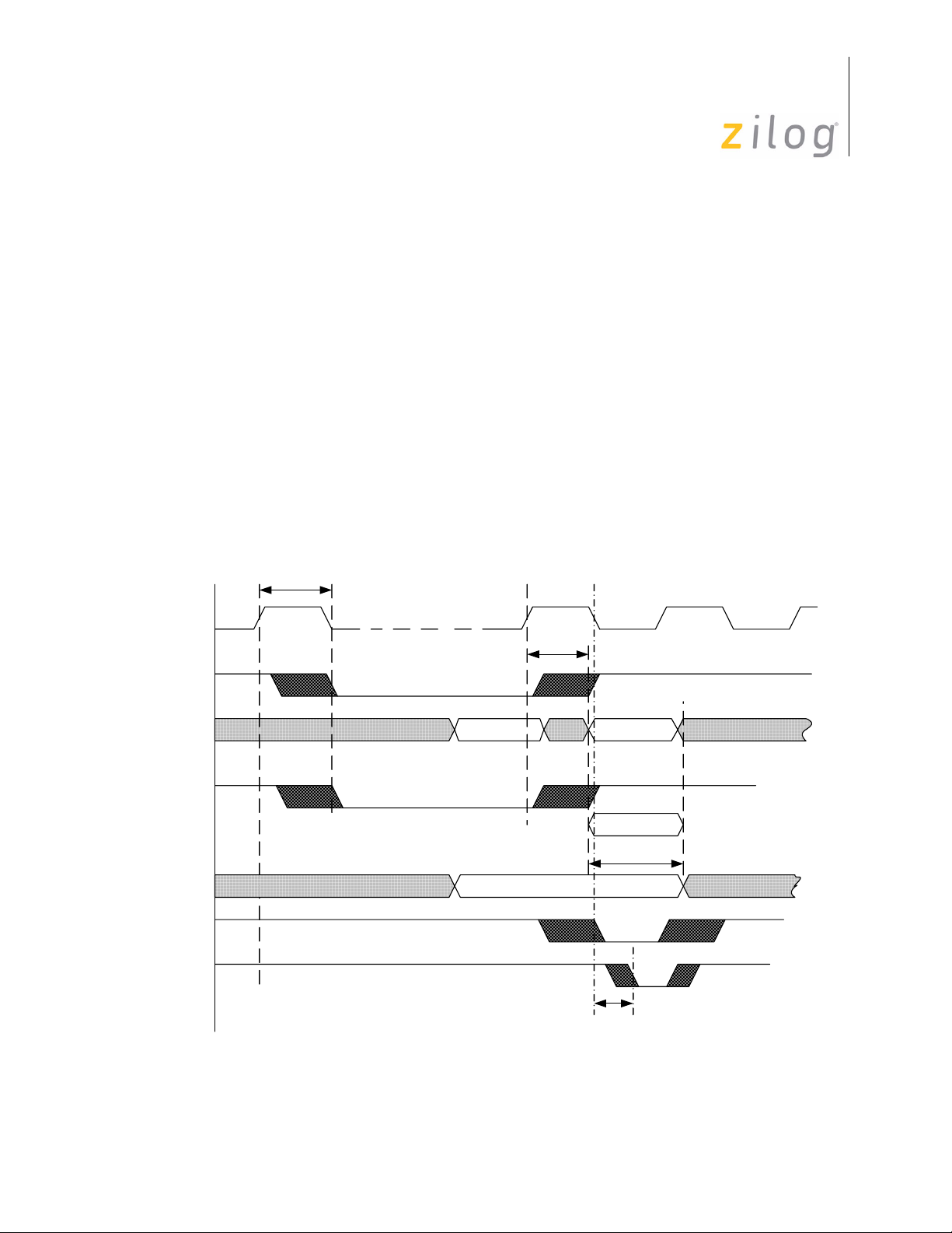
Zdots® SBC for eZ80AcclaimPlus!™ Connectivity ASSP
Product Specification
going into High-Z mode, that is, after the end of the eZ80F91 Read access to Flash, it
takes 8.8 ns+25 ns = 33.8 ns before Flash stops driving the data bus. At this point, the
eZ80F91 device is already well into the next bus cycle.
Consider the next cycle to be Memory Write. During the Memory Write cycle, data (output) from the eZ80F91 device is valid not later than T3 = 7.5 ns, and the Write pulse is
asserted not later than 4.5 ns after the falling edge of the Clock (14.5 ns from the rising
edge if Clock is 50 MHz). It means that during T
= (33.8 ns – 7.5 ns) = 26.3 ns; two
CON
devices drive the common Data Bus—the eZ80F91 device and Flash. In turn, data that is
being written during the Write operation might be corrupted. The part used to isolate a
slow Flash data bus from a fast eZ80F91 bus has 5.5 ns turn-off time, which reduces 25 ns
part of the T
to 5.5 ns. As a result, bus contention still occurs, but its duration is not
CON
26.3 ns, as described in the following equation:
14
Clock
-CS0
F91 Data
Bus
-RD
FLash
Data Bus
-CS1
Time of contention 8.8 ns
-7.5 ns 5.5 ns+()6.8 ns==
Data being written is not corrupted because the Write pulse is not yet asserted.
T6
T3
Data IN Data OUT
Bus contention
Tod
-WR
T4
Figure 4. Bus Contention without the Zdots Fast Buffer Feature
PS026102-1207 Onboard Component Description
Page 19

Zdots® SBC for eZ80AcclaimPlus!™ Connectivity ASSP
Product Specification
Memory
The Zdots contains external Flash memory and the eZ80F91 connectivity ASSP contains
internal Flash memory. To allow Read/Write access to Flash memory on the Zdots, there
are two signals provided on connectors JP1 and JP2. A jumper JP3 on the module enables
programming of on-chip Flash.
There is also a signal that duplicates the function of this jumper. Table 4 describes the
states of the signals and the status of the jumper for different modes.
Table 4. Flash Memory Programming Signals and Jumpers
Signal/Jumper Function State/Status
15
DIS_FLASH
F
lashWE Controls Write operations to the boot block of Zdots for
JP3
F91_WE
Controls Read/Write access to Zdots for eZ80AcclaimPlus!
ASSP external Flash memory
eZ80AcclaimPlus! ASSP external Flash memory
Controls Write access to eZ80F91 MCU on-chip Flash memory When IN, Write is
Controls Write access to eZ80F91 MCU on-chip Flash memory When Low, Write is
The external Flash memory of Zdots has an access time of 100 ns. At least five wait states
must be added to the cycle when accessing external Flash at 50 MHz clock speed. The
eZ80F91 devices on-chip Flash is faster; its minimum access time is 60 ns, which requires
only three wait states at 50 MHz.
There is 512 KB of fast SRAM on the Zdots. Access time is 12 ns, which requires one
wait-state access. The eZ80F91’s on-chip SRAM is used with zero wait states.
IrDA Transceiver
An onboard IrDA transceiver (Zilog ZHX1810) is connected to PD0 (TX), PD1 (RX), and
PD2 (Shutdown, R_SD). The IrDA transceiver is of the LED type 870 nm Class 1.
When Low, access
is enabled
When Low, Write is
enabled
enabled
enabled
The receiver supply current is 90–150 µA and the transmitter supply current is 260 mA
when the LED is active. The IrDA transceiver is accessible via the IrDA controller
attached to UART0 on the eZ80F91 device. The UART0 console and the IrDA transceiver
cannot be used simultaneously.
To use the UART0 for console or to save power, the transceiver is disabled by the software
or by an off-board signal when using the proper jumper selection. The transceiver is
PS026102-1207 Onboard Component Description
Page 20

disabled by setting PD2 (IR_SD) High or by pulling the DIS_IRDA pin on the I/O
connector Low. The shutdown is used for power savings. To enable the IrDA transceiver,
DIS_IRDA
Reset Generator
The onboard Reset Generator Chip performs reliable Power-On Reset. The chip generates
a reset pulse with a duration of 200 ms if the power supply drops below 2.93 V. This reset
pulse ensures that the board always starts in a defined condition. The RESET pin on the
I/O connector reflects the status of the RESET line. It is a bidirectional pin for resetting
external peripheral components or for resetting the Zdots with a low-impedance output
(for example, a 100 Ω push button).
Zdots® SBC for eZ80AcclaimPlus!™ Connectivity ASSP
Product Specification
16
is left floating and PD2 is set to Low.
Serial Interface Ports
The CPU contains two UARTs with programmable baud rate generators. UART0 is connected to GPIO PD[0:7] on the I/O connector. UART1 is connected to GPIO PC[0:7] on
the I/O connector.
Note:
Do not connect an RS-232 interface without level shifters. There are no
RS-232 level shifters on the Zdots.
Physical Dimensions
The footprint of the Zdots PCB is 63.5 mm x 78.7 cm. With an RJ-45 Ethernet connector,
the overall height is 25 mm, see Figure 5 on page 17.
PS026102-1207 Onboard Component Description
Page 21

16.5 mm
Zdots® SBC for eZ80AcclaimPlus!™ Connectivity ASSP
Product Specification
17
56.0 mm
C18C19C20C21
C40
eZ80F91 MODULE
Y1
U4
R4
U2
R23
R16
R24
R25 R28
U6
R37
R3
C1
C22
+
VL1
U1
R29
R14R15
R21
R13
R19
CR1
U5
R10
C3
JP2
Zilog PCA: 99C0879-001
COPYRIGHT Zilog XTOOLS 2002
Y2
U3
78.7 mm
JP1
2
1
P2
C42
JP3
ISO
C12
C11
R17
R18
R36
R22
R20
U8
Y3
R6
31.8 mm
63.5 mm
Figure 5. Physical Dimensions of the Zdots SBC
PS026102-1207 Onboard Component Description
Page 22

Zdots® SBC for eZ80AcclaimPlus!™ Connectivity ASSP
Figure 6 displays the top layer silk-screen of the Zdots.
Product Specification
18
JP1
2
1
P2
R17
JP3
R18
R36
R22
ISO
R20
U8
C12
C11
C42
Y3
R6
C18C19C20C21
C40
eZ80F91 MODULE
Y1
U4
R4
U2
R23
R16
R24
R25 R28
U6
+
VL1
C22
U1
R37
R3
C1
R29
R14R15
R21
R13
R19
CR1
U5
JP2
1
Zilog PCA: 99C0879-001
COPYRIGHT Zilog XTOOLS 2002
Y2
C3
R10
U3
Figure 6. Zdots Module—Top Layer
PS026102-1207 Onboard Component Description
Page 23

Zdots® SBC for eZ80AcclaimPlus!™ Connectivity ASSP
Figure 7 displays the bottom layer silk-screen of the Zdots.
Product Specification
19
JP2 JP1
1
C9
R9
DJP 2002
C14
C39
C35
C26
C36
L1
C38
R27
C10
C8
R26
R8
R7
C6
R2
R1
R30
R12
R5
C2
Zilog FAB: 98C0879-001 REV A
C25
C34
C27
C24
C5
C37
C51
C50
C49
C48
C32
C28
C23
C41
MADE IN U.S.A.
C4
C7
C52
C53
C44
C45
C46C47
C33
C29
U9
U10
C43
R34R35
C16
R11
R33
R31 R32
C17
C30
C31
2
C13
C15
Figure 7. Zdots Module—Bottom Layer
Absolute Maximum Ratings
Stresses greater than those listed in Table 5 causes permanent damage to the device. These
ratings are stress ratings only. Operation of the device at any condition outside those indicated in the operational sections of these specifications is not implied. Exposure to absolute maximum rating conditions for extended periods may affect device reliability. For
improved reliability, unused inputs must be tied to one of the supply voltages (V
V
).
SS
Table 5. Absolute Maximum Ratings
Parameter Minimum Maximum Units
Standard operating temperature 0 +70 ºC
Storage temperature –45 +85 ºC
PS026102-1207 Onboard Component Description
DD
or
Page 24

Zdots® SBC for eZ80AcclaimPlus!™ Connectivity ASSP
Table 5. Absolute Maximum Ratings (Continued)
Parameter Minimum Maximum Units
Operating Humidity (RH @ 50 ºC) 25% 90%
Operating Voltage — 3.6 V
Zdots Bill of Materials
Table 6 lists the installed components of the Zdots.
Table 6. Bill of Materials for the Zdots
Part Number Part Name Quantity
Product Specification
20
Jumper
Location Manufacturer
98C0879-001 Fab, Rev. B 1 — Prime Technologies
35-0180-12 IC, SRAM, 512Kx8, 12 ns, 3 V, 36-SOJ 1 U8 Alliance Semi.
AS7C34096-12JC
35-0016-05 IC, 74LVC04, 3.3 V, GATE, 14-SOIC 1 U1 Texas Instruments
SN74LVC04AD
35-0720-10 IC, Flash, 1Mx8, 100 ns, 3 V, 40-TSSOP 1 U9 AMD AM29LV008BB-
90ED
35-0719-00 IC, MAX6328, RESET, SOT-23 1 U3 Maxim Inc.
MAX6328UR29-T
ZHX1810 IC, IR Transceiver, Low Profile 1 U2 Zilog
35-0062-01 IC, 74LCX32, LV, QUAD OR, 14-TSSOP 1 U4 Fairchild Semi.
35-0022-01 IC, AM7C874, PHY XCVR, 80QFP 1 U6 AMD AM79C874VC
eZ80F91 IC, eZ80F91, 50 MHZ, 144VQFP 1 U5 Zilog Inc. eZ80F91
35-0731-00 IC, 74CBTLV3861PWR, 24-TSSOP 1 U10 Texas Instruments
48-1013-01 Diode, TVS Array, XCVR Prot, 8-SOIC 1 U9 Semtec
®
Inc.
ZHX1810MV115THTR
74LCX32MTC
SN74CBTLV3861PWR
LCDA15C-6
17-2005-70 CAP, 1000 pF, 50 V, Ceramic Chip,
0603
17-2005-66 CAP, 0.1 µF, 16 V, Ceramic Chip, 0603 28 C2,10, C15-
17-2005-54 CAP, 0.01 µF, 50 V, Ceramic Chip, 0603 1 C3 Panasonic
PS026102-1207 Onboard Component Description
15 C13, C14,
C31-43
30, C44-53
Panasonic
ECJ-1VC1H561J
Kemet Inc.
C0603C104K5RAC
ECJ-1VB1C103K
Page 25

Zdots® SBC for eZ80AcclaimPlus!™ Connectivity ASSP
Product Specification
Table 6. Bill of Materials for the Zdots (Continued)
Jumper
Part Number Part Name Quantity
17-2005-83 CAP, 0.33 µF, 16 V, Ceramic Chip, 0603 1 C1 Panasonic
17-2005-63 CAP, 560 pF, 50 V, Ceramic Chip, 0603 1 C6 Panasonic
Location Manufacturer
ECJ-1VF1C334Z
ECJ-1VC1H563K
21
17-2001-03 CAP, 12 pF, 50 V, Ceramic Chip, 0603 4 C9, C11,
C12
17-2001-05 CAP, 22 pF, 50 V, CER CHIP, 0603 2 C4, C7 PANASONIC
17-2001-20 CAP, 270 pF, 50 V, CER CHIP, 0603 1 C5 PANASONIC
17-2001-01 CAP, 5 pF, 50 V, CER CHIP, 0603 1 C8 PANASONIC
48-0051-00 DIODE, 1N5817, RCTFR 1 CR1 MOTOROLA
16-9005-33 INDUCTOR, 3.3 µH, 20%, 1210 SMD 1 L1 PANASONIC
46-3001-03 Resistor, 10 K¾, 1%, 1/16 W, 0603 SMT 15 R3, 8, 10,
R12-18,
R20, 25, 29,
30, 37
46-3000-00 Resistor, 0 ¾, 1%, 1/16 W, 0603 SMT 4 R19, 21, 23,
24
46-3000-71 Resistor, 2.21 K¾, 1%, 1/16W, 0603
SMT
2R5, R6
Panasonic
ECJ-1VC1H120J
ECJ-1VC1H220J
ECJ-1VC1H271J
ECJ-1VC1H050C
1N5817
ELJ-PA3R3MF
Sprague
420CK472X2PD
46-3000-35 Resistor, 68 ¾, 1%, 1/16 W, 0603 SMT 1 R3
46-3000-02 RES, 2.2 ¾, 1%, 1/16W, 0603 SMT 1 R4
46-3000-32 RES, 49.9 ¾, 1%, 1/16W, 0603 SMT 4 R11, 31, 32,
33
46-3000-63 RES, 1 K¾, 1%, 1/16W, 0603 SMT 1 R22
46-3000-56 RES, 499 ¾,1%, 1/16W, 0603 SMT 1 R26
46-3001-34 RES, 200 K¾, 1%, 1/16W, 0603 SMT 1 R27
46-3000-47 RES, 221 ¾, 1%, 1/16W, 0603 SMT 1 R28
46-3000-51 RES, 332 ¾, 1%, 1/16W, 0603 SMT 2 R34, R35
46-3001-75 RES, 10 M¾, 1%, 1/16W, 0603 SMT 1 R38
PS026102-1207 Onboard Component Description
Page 26

Zdots® SBC for eZ80AcclaimPlus!™ Connectivity ASSP
Table 6. Bill of Materials for the Zdots (Continued)
Part Number Part Name Quantity
Product Specification
22
Jumper
Location Manufacturer
23-0000-25 XTAL, 25.0000 MHz, SER/RESN,
HC49S
23-0000-50 XTAL, 50.0000 MHz, SER/RESN,
HC49S
23-0006-00 Internal crystal, 32.768 kHz, SER/RESN,
TF case
21-0907-01 Connector, RJ45, Fast jack,10/100
Base-T
21-0055-02 Connector, HDR/PIN, .025SQ, double
row
1 Y1 CITIZEN
HC49US25.000MABJ
1 Y2 CITIZEN
HC49US50.000MABJ
1 Y3 Fox NC-38
1 P2 Halo Electronics
HFJ11-2450E-L11
2JP1, JP2
(backside)
Harwin
M-20-976-3622
PS026102-1207 Onboard Component Description
Page 27
Zdots® SBC for eZ80AcclaimPlus!™ Connectivity ASSP
Product Specification
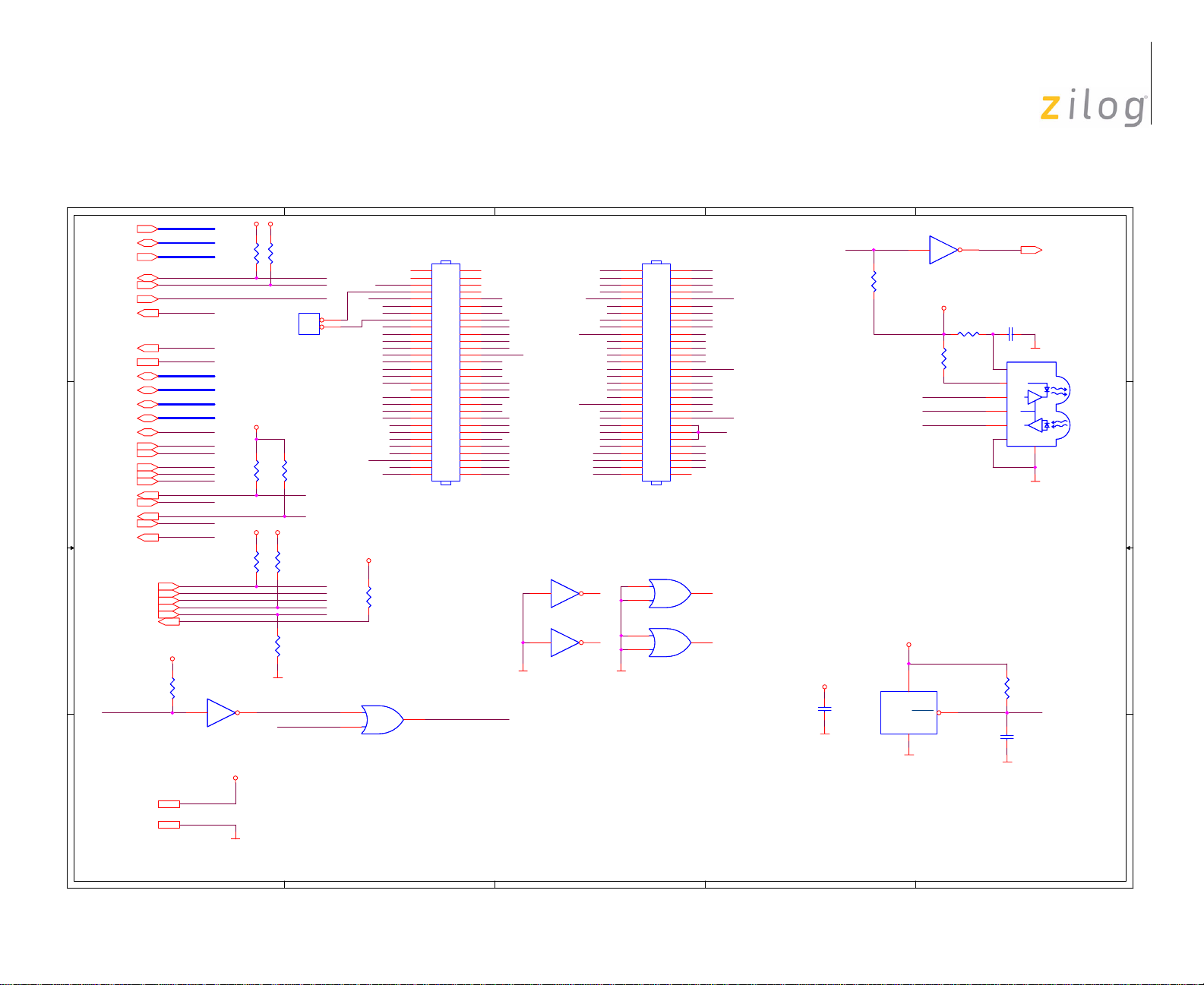
Schematics
Figure 8 through Figure 10 displays the layout of the Zdots. Ethernet circuiting devices are not loaded on the Zdots. However, these devices appear
in the following schematics for reference.
5
TDI
TDO
TRIGOUT
TCK
TMS
-TRSTN
VCC
GND
A[0..23]
D[0..7]
-CS[0..3]
IICSDA
IICSCL
CLK_OUT
-DIS_FLASH
-FLASHWE
RTC_VDD
PA[0..7]
PB[0..7]
PC[0..7]
PD[0..7]
-RESET
-RD
-WR
-IOREQ
-MREQ
-INSTRD
-HALT_SLP
-BUSREQ -BUSREQ
-BUSACK
-NMI
VCC
R12
R12
10K
10K
5 6
GND
A[0..23]
D[0..7]
-CS[0..3]
IICSDA
IICSCL
CLK_OUT
D D
-DIS_FLASH
-FLASHWE
RTC_VDD
PA[0..7]
PB[0..7]
PC[0..7]
PD[0..7]
-RESET
-RD
C C
B B
A A
-WR
-IOREQ
-MREQ
-INSTRD
-WAIT
-HALT_SLP
-BUSREQ
-BUSACK
-DIS_IRDA
-NMI
U1C
U1C
74LCX04
74LCX04
TSSOP14
TSSOP14
VCC
VCC
VCC
R1
R2
4.7KR24.7K
4.7KR14.7K
IICSDA
IICSCL
EZ80CLK
JP3JP3
1
2
WR_EN
VCC
R5
R6
2.2KR52.2K
2.2KR62.2K
-WAIT-WAIT
VCCVCC
R7
R8
10KR810K
10KR710K
TDI
TDO
TRIGOUT
TCK
TMS
-TRSTN
R9
4.7KR94.7K
DISABLE_IRDA
=
IR_SD
PD2
VCC
GND
4
connector 1
JP1
JP1
2
1
4
3
-TRSTN
-F91_WE
GND GND
A6
A10
GND
A8
A13
A15
A18
A19
A2
A11
A4
A5
A21
A22
-CS0
-CS2
D1
D3
D5
D7
-MREQ
GND
-WR
-BUSACK
VCC
R20
R20
10K
10K
U4B
U4B
4
5
74LCX32
74LCX32
TSSOP14
TSSOP14
6
5
7
9
11
13
15
17
19
21
23
25
27
29
31
33
35
37
39
41
43
45
47
49
51
53
55
57
59
HEADER 30x2/SM
HEADER 30x2/SM
6
8
10
12
14
16
18
20
22
24
26
28
30
32
34
36
38
40
42
44
46
48
50
52
54
56
58
60
IRDA_SD
A0
A3
VCC
A7
A9
A14
A16
GND
A1
A12
A20
A17
-DIS_FLASH
VCC
A23
-CS1
D0
D2
D4
GND
D6
-IOREQ
-RD
-INSTRD
-BUSREQ
3 4
13 12
GND GND
U1B
U1B
74LCX04
74LCX04
TSSOP14
TSSOP14
U1F
U1F
74LCX04
74LCX04
TSSOP14
TSSOP14
3
connector 2
PA7
PA5
PA3
PA1
VCCVCC
PB7
11
PB5
13
PB3
15
PB1
17
GND
19
PC6
21
PC4
23
PC2
25
PC0
27
PD6
29
PD5
31
PD3
33
PD1
35
TDO
37
GND
39
TCK
41
RTC_VDD
43
IICSCL
45
IICSDA
47
-FLASHWE
49
-CS3
51
-RESET
53
VCC
55
-HALT_SLP
57
VCC
59
This schematic reflects the
assembly rev B of the module.
The FLASH memory on page 3
was changed to AM29008B for
Rev D schematic.
JP2
JP2
1
3
5
7
9
HEADER 30x2/SM
HEADER 30x2/SM
U4A
U4A
1
2
74LCX32
74LCX32
TSSOP14
TSSOP14
U4D
U4D
12
13
74LCX32
74LCX32
TSSOP14
TSSOP14
2
U1A
VCC
3
VDD
RESET
GND
1
U1A
1 2
74LCX04
74LCX04
TSSOP14
TSSOP14
VCC
R4
2R7R42R7
PD0
IRDA_SD
PD1
U3
U3
2
open-drain
MAX6328UR29
MAX6328UR29
SOT-23-L3
SOT-23-L3
R3
68RR368R
(MMA 0204)
-F91_WE -F91_WP
PA6
2
PA4
4
PA2
6
PA0
8
10
PB6
12
PB4
14
PB2
16
PB0
18
PC7
20
PC5
22
PC3
24
PC1
26
PD7
28
GND
30
PD4
32
PD2
34
PD0
36
TDI
38
TRIGOUT
40
TMS
42
EZ80CLK
44
46
GND
48
50
-DIS_IRDA
52
-WAIT
54
GND
56
-NMI
58
60
3
11
VCC
C2
0.1uFC20.1uF
R37
R37
10K
10K
alternative:
Maxim
MAX6802UR29D3
1
-F91_WP
C1
330nFC1330nF
U2
5
VCC
1
LEDA
2
TXD
4
SD
3
RXD
6
GND
T
ZHX1810U2ZHX1810
0
R10
R10
10K
10K
-RESET
C3
0.01uFC30.01uF
Memory
23
5
4
3
2
1
Figure 8. Zdots Schematic Diagram—Connectors and Miscellaneous
PS026102-1207 Schematics
Page 28

Zdots® SBC for eZ80AcclaimPlus!™ Connectivity ASSP
Product Specification
24
5
D[0:7]
D D
GND
C C
B B
RTC_VDD
VCC
A A
C5
220pFC5220pF
Y2
50MHzY250MHz
R27
R27
C8
5pFC85pF
C10
C10
0.1uF
0.1uF
RTC_VDD
21
CR1
CR1
1N5817
1N5817
R28
R28
220
220
VL1VL1
-WAIT
-NMI
TMS
TCK
TDI
R26
R26
499
499
L1
3.3uHL13.3uH
32.768KHz
32.768KHz
10M
10M
-BUSREQ
-TRSTN
-RESET
-F91_WP
VCC
C12
C12
12pF
12pF
-BUSREQ
-TRSTN
-RESET
-F91_WP
C6
0.056uFC60.056uF
C9
200K
200K
10pFC910pF
Y3
Y3
R38
R38
C11
C11
12pF
12pF
GND GND
5
D0
D1
D2
D3
D4
D5
D6
D7
-WAIT
-NMI
TMS
TCK
TDI
CRS
COL
RXER
RXDV
RXD3
RXD2
RXD1
RXD0
RXCLK
TXCLK
144
124
125
135
137
141
140
139
138
136
131
112
122
133
108
113
123
134
39
40
41
42
43
44
45
46
54
57
56
66
67
69
71
55
83
86
85
6
14
22
31
37
47
59
81
88
98
87
7
15
23
32
38
48
60
64
72
82
89
99
84
63
62
61
U5
D0
D1
D2
D3
D4
D5
D6
D7
WAIT
BUSREQ
NMI
TMS
TCK
TDI
TRSTN
RESET
WP
MII_CRS
MII_COL
MII_RXER
MII_RXDV
MII_RXD3
MII_RXD2
MII_RXD1
MII_RXD0
MII_RXCLK
MII_TXCLK
FILT_IN
XIN
XOUT
VDD
VDD
VDD
VDD
VDD
VDD
VDD
VDD
VDD
VDD
VDD
VDD
VDD
PLL_VDD
VSS
VSS
VSS
VSS
VSS
VSS
VSS
VSS
VSS
VSS
VSS
VSS
VSS
VSS
VSS
VSS
PLL_VSS
RTC_VDD
RTC_XOUT
RTC_XIN
EZ80F91U5EZ80F91
PA6_PWM2_EC1
PA5_PWM1_TOUT1
PA4_PWM0_TOUT0
PA3_PWM3_OC3
PA2_PWM2_OC2
PA1_PWM1_OC1
PA0_PWM0_OC0
PD1_RXD0_IRRXD
PD0_TXD0_IRTXD
MII_TXD3
MII_TXD2
MII_TXD1
MII_TXD0
MII_TXEN
MII_TXER
MII_MDC
MII_MDIO
IORQ
MRQ
BUSACK
CS0
CS1
CS2
CS3
SCL
SDA
PA7_PWM3
PB7_MOSI
PB6_MISO
PB5_ICB3
PB4_ICA3
PB3_SCK
PB2_SS
PB1_IC1
PB0_IC0_EC0
PC7_RI1
PC6_DCD1
PC5_DSR1
PC4_DTR1
PC3_CTS1
PC2_RTS1
PC1_RXD1
PC0_TXD1
PD7_RI0
PD6_DCD0
PD5_DSR0
PD4_DTR0
PD3_CTS0
PD2_RTS0
HALT_SLP
INSTRD
TDO
TRIGOUT
4
A0
1
A0
A1
2
A1
A2
3
A2
A3
4
A3
A4
5
A4
A5
8
A5
A6
9
A6
A7
10
A7
A8
11
A8
A9
12
A9
A10
13
A10
A11
16
A11
A12
17
A12
A13
18
A13
A14
19
A14
A15
20
A15
A16
21
A16
A17
24
A17
A18
25
A18
A19
26
A19
A20
27
A20
A21
28
A21
A22
29
A22
A23
30
A23
RD
WR
PHI
TXD3
126
TXD2
127
TXD1
128
TXD0
129
TXEN
130
TXER
132
MDC
142
MDI0
143
-IORQ
49
-MREQ
50
-RD
51
-WR
52
58
-CS0
33
-CS1
34
-CS2
35
-CS3
36
SCL
110
SDA
109
PA7
121
PA6
120
PA5
119
PA4
118
PA3
117
PA2
116
PA1
115
PA0
114
PB7
107
PB6
106
PB5
105
PB4
104
PB3
103
PB2
102
PB1
101
PB0
100
PC7
97
PC6
96
PC5
95
PC4
94
PC3
93
PC2
92
PC1
91
PC0
90
PD7
80
PD6
79
PD5
78
PD4
77
PD3
76
PD2
75
PD1
74
PD0
73
65
111
53
70
68
-IORQ
-MREQ
-RD
-WR
-BUSACK
-CS0
-CS1
-CS2
-CS3
IICSCL
IICSDA
A[0:23]
GND
PA[0:7]
PB[0:7]
PC[0:7]
PD[0:7]
-HALT_SLP
CLK_OUT
-INSTRD
TDO
TRIGOUT
VCC
R221KR22
1K
3
R18
R18
10K
10K
-RESET
MDI0
MDC
RXCLK
RXD3
RXD2
RXD1
RXD0
RXDV
RXER
TXCLK
TXD3
TXD2
TXD1
TXD0
TXEN
TXER
COL
CRS
C44
C44
C45
C45
0.1uF
0.1uF
0.1uF
0.1uF
C49
C49
C50
C50
0.1uF
0.1uF
0.1uF
0.1uF
GND
Put caps between pairs of U6, 10:11, 51:52, 59:65
and 71:73 as close to the pins as possible
C31
C31
C32
C32
0.001uF
0.001uF
0.001uF
0.001uF
C19
C19
C18
C18
0.1uF
0.1uF
0.1uF
0.1uF
VCC
VCC
U6
U6
1
PCSB
2
ISODEF
3
ISO
5
REFCLK
7
BURN_IN
8
RST
9
PWRDN
14
PHYAD4_0RXD-
15
PHYAD3_10RXD+
16
PHYAD2_10TXD++
17
PHYAD1_10TXD-
18
PHYAD0_10TXD--
19
GPIO0_10TXD--
20
GPIO1_TP125
21
MDIO
22
MDC
30
RXCLK
23
RXD3
24
RXD2
25
RXD1
26
RXD0
29
RXDV
31
RXER_RXD4
33
TXCLK_PCSBPCLK
40
TXD3
39
TXD2
38
TXD1
37
TXD0
34
TXEN
32
TXER_TXD4
41
COL
42
CRS
AM79C874
AM79C874
C46
C46
0.1uF
0.1uF
C51
C51
0.1uF
0.1uF
C33
C33
0.001uF
0.001uF
C20
C20
0.1uF
0.1uF
VCC
GND
TGND14PLLGND11OGND112DGND128DGND235OGND250CRVGND51EQGND65REFGND71TGND2
C47
C47
0.1uF
0.1uF
C52
C52
0.1uF
0.1uF
C34
C34
0.001uF
0.001uF
C21
C21
0.1uF
0.1uF
13
10
PLLVCC
C48
C48
0.1uF
0.1uF
VCC
C53
C53
0.1uF
0.1uF
C35
C35
0.001uF
0.001uF
C22
C22
0.1uF
0.1uF
OVDD1
36
49
VDD127VDD2
2
VCC
73
80
52
59
60
TVCC179TVCC2
OVDD2
EQVCC
REFVCC
CRVVCC
ADOVCC
LEDSPD0_LEDBTA_FXSEL
LECOL_SCRAMEN
LEDRX_LEDSEL
LEDTX_LEDBTB
LEDLNK_LED_10LNK
LESPD1_LEDTXA_CLK25EN
LEDDPX_LEDTXB
TEST1_FXR+
TEST0_FXR-
76
GND
C37
C37
C36
C36
0.001uF
0.001uF
0.001uF
0.001uF
C23
C23
C24
C24
0.1uF
0.1uF
0.1uF
0.1uF
INTR
TECH_SEL2
TECH_SEL1
TECH_SEL0
ANEGA
IBREF
RPTR
TEST3_SDI+
TEST2
FXT+
FXT-
XTL-
XTL+
TX+
RX+
RX-
VCC
R34
R34
330
330
1
R13
R13
R14
R14
10K
10K
10K
0
0
C16
C16
0.1uF
0.1uF
-LEDRX
-LEDLNK
C41
C41
0.001uF
0.001uF
C28
C28
0.1uF
0.1uF
Y1
25 MHzY125 MHz
10K
43
53
54
55
56
72
61
44
45
-LEDRX
46
47
-LEDLNK
48
57
58
62
68
67
66
69
70
74
75
77
78
TX-
64
63
R11
R11
49.9
49.9
R32
R32
R31
49.9
R31
49.9
R35
R35
330
330
R33
R33
C38
C38
C39
C39
0.001uF
0.001uF
0.001uF
0.001uF
C26
C26
C25
C25
0.1uF
0.1uF
0.1uF
0.1uF
R190R19
R210R21
R240R24
R230R23
0
0
This schematic reflects the
assembly rev B of the
module.
The FLASH memory on page 3
was changed to AM29008B for
Rev D schematic.
49.9
49.9
49.9
49.9
C15
C15
0.1uF
0.1uF
C40
C40
0.001uF
0.001uF
C27
C27
0.1uF
0.1uF
R15
R15
10K
10K
R25
R25
C4
C7
C42
C42
0.001uF
0.001uF
C29
C29
0.1uF
0.1uF
GND
R16
R16
10K
10K
10K
10K
18pFC418pF
18pFC718pF
GND
VCC
P2
P2
1
TX+
4
TXCT
2
TX-
3
RX+
5
RXCT
6
RX-
8
GND
9
AN1
10
CT1
11
AN2
12
CT2
HFJ11-2450E-L11
HFJ11-2450E-L11
VCC
C43
C43
0.001uF
0.001uF
GND
C30
C30
0.1uF
0.1uF
VCC
10K 0.1%
10K 0.1%
C17
C17
0.1uF
0.1uF
R17
R17
CPU and PHY
4
GND
3
2
1
Figure 9. Zdots Schematic Diagram—CPU and PHY
PS026102-1207 Schematics
Page 29

Zdots® SBC for eZ80AcclaimPlus!™ Connectivity ASSP
Product Specification
25
5
-DIS_FLASH
-RD
-WR
-CS0
-RESET
-FLASHWE
-CS1
VCC
VCC
A0
A1
A2
A3
A4
A5
A6
A7
A8
A9
A10
A11
A12
A13
A14
A15
A16
A17
A19
C13
C13
0.001uF
0.001uF
-CS1
D D
D[0:7]
-DIS_FLASH
-RD
-WR
-CS0
-RESET
-FLASHWE
A[0..23] A[0..23]
VCC
C14
C14
0.001uF
0.001uF
A[0:23]
C C
B B
A A
4
U8
U8
A18
1
A0
A0
2
A1
A1
3
A2
A2
4
A3
A3
5
A4
-CS1
6
VCC VCC
VCC
31
U11
U11
21
A0
20
A1
19
A2
18
A3
17
A4
16
A5
15
A6
14
A7
8
A8
7
A9
36
A10
6
A11
5
A12
4
A13
3
A14
2
A15
1
A16
40
A17
13
A18
37
A19
R29
R29
10K
10K
VCC130VCC2
RESET
GND123GND2
Am29LV008B
Am29LV008B
39
25
DQ0
26
DQ1
27
DQ2
28
DQ3
32
DQ4
33
DQ5
34
DQ6
35
DQ7
22
CE
24
OE
9
WE
10
12
RY/BY
11
NC1
29
NC3
38
NC2
U1D
U1D
9 8
74LCX04
74LCX04
TSSOP14
TSSOP14
CE
7
I/O0
D1 D6
8
I/O1
9
VDD
10
VSS
11
I/O2
D3
12
I/O3
-WR
13
WE
A12
14
A5
A9
15
A6
A6
16
A7
A4
17
A8
A17
18
A9
512kx8 SRAM
512kx8 SRAM
SOJ36.400
SOJ36.400
DFLASH0
DFLASH1
DFLASH2
DFLASH3
DFLASH4
DFLASH5
DFLASH6
DFLASH7
-CSFLASH
-RD
-WR
-RESET
-WP
VCC
A21A18
A20
-CS0
-FLASH_EN
VCC VCC
R30
R30
10K
10K
9
10
U1E
U1E
11 10
74LCX04
74LCX04
TSSOP14
TSSOP14
N.C.
A18
A17
A16
A15
OE
I/O7
I/O6
VSS
VDD
I/O5
I/O4
A14
A13
A12
A11
A10
N.C.
U4C
U4C
74LCX32
74LCX32
TSSOP14
TSSOP14
-WP
36
35
34
33
32
31
30
29
28
27
26
25
24
23
22
21
20
19
3
A8
A7
A5
2
3
4
5
6
7
8
9
10
11
23
1
8
A16
A15
A14
A13
-RD
D7D0
D5D2
D4
A11
A10
U10
U10
A1
A2
A3
A4
A5
A6
A7
A8
A9
A10
B10
VCC
OE
NC
GND
SN74CBTLV3861
SN74CBTLV3861
-CSFLASH
2
VCC
D0
D1
D2
D3
D4
D5
D6
D7
22
B1
21
B2
20
B3
19
B4
18
B5
17
B6
16
B7
15
B8
14
B9
13
24
12
1
This schematic reflects the
assembly rev B of the module.
The FLASH memory on page 3
was changed to AM29008B for
VCC
GND
GND
Rev D schematic.
Memory
5
4
3
2
1
Figure 10. Zdots Schematic Diagram—Module Memory
PS026102-1207 Schematics
Page 30

Zdots® SBC for eZ80AcclaimPlus!™ Connectivity ASSP
Customer Support
For answers to technical questions about the product, documentation, or any other issues
with Zilog’s offerings, please visit Zilog’s Knowledge Base at
http://www.zilog.com/kb
For any comments, detail technical questions, or reporting problems, please visit Zilog’s
Technical Support at http://support.zilog.com
.
Product Specification
26
.
PS026102-1207 Customer Support
 Loading...