

Page 1

eZ80F915005MODG
eZ80F91 Mini Enet Module
Product Specification
PS023603-0907
PRELIMINARY
Copyright ©2007 by Zilog®, Inc. All rights reserved.
www.zilog.com
Page 2

Warning:
DO NOT USE IN LIFE SUPPORT
LIFE SUPPORT POLICY
ZILOG'S PRODUCTS ARE NOT AUTHORIZED FOR USE AS CRITICAL COMPONENTS IN LIFE
SUPPORT DEVICES OR SYSTEMS WITHOUT THE EXPRESS PRIOR WRITTEN APPROVAL OF
THE PRESIDENT AND GENERAL COUNSEL OF ZILOG CORPORATION.
As used herein
Life support devices or systems are devices which (a) are intended for surgical implant into the body, or (b)
support or sustain life and whose failure to perform when properly used in accordance with instructions for
use provided in the labeling can be reasonably expected to result in a significant injury to the user. A
critical component is any component in a life support device or system whose failure to perform can be
reasonably expected to cause the failure of the life support device or system or to affect its safety or
effectiveness.
Document Disclaimer
©2007 by Zilog, Inc. All rights reserved. Information in this publication concerning the devices,
applications, or technology described is intended to suggest possible uses and may be superseded. ZILOG,
INC. DOES NOT ASSUME LIABILITY FOR OR PROVIDE A REPRESENTATION OF ACCURACY
OF THE INFORMATION, DEVICES, OR TECHNOLOGY DESCRIBED IN THIS DOCUMENT.
ZILOG ALSO DOES NOT ASSUME LIABILITY FOR INTELLECTUAL PROPERTY
INFRINGEMENT RELATED IN ANY MANNER TO USE OF INFORMATION, DEVICES, OR
TECHNOLOGY DESCRIBED HEREIN OR OTHERWISE. The information contained within this
document has been verified according to the general principles of electrical and mechanical engineering.
Z8, Z8 Encore!, Z8 Encore! XP, Z8 Encore! MC, Crimzon, eZ80, and ZNEO are trademarks or registered
trademarks of Zilog, Inc. All other product or service names are the property of their respective owners.
PS023603-0907 P R E L I M I N A R Y
Page 3

Revision History
Each instance in Revision History reflects a change to this document from its previous
revision. For more details, refer to the corresponding pages and appropriate links in the
table below.
Revision
Date
Level Description Page No
eZ80F91 Mini Enet Module
Product Specification
iii
August 2007 3 Changed eZ80F915005MOD to
eZ80F915005MODG
August 2004 2
May 2004 1 Original issue All
Added new dimensions figure for the
module
i
All
PS023603-0907 P R E L I M I N A R Y Revision History
Page 4

Table of Contents
eZ80F91 Mini Enet Module . . . . . . . . . . . . . . . . . . . . . . . . . . . . . . . . . . . . . . . . 1
Module Features . . . . . . . . . . . . . . . . . . . . . . . . . . . . . . . . . . . . . . . . . . . . . . . . . 1
eZ80F91 Controller Features . . . . . . . . . . . . . . . . . . . . . . . . . . . . . . . . . . . . . . . 2
Block Diagram . . . . . . . . . . . . . . . . . . . . . . . . . . . . . . . . . . . . . . . . . . . . . . . . 3
Pin Description . . . . . . . . . . . . . . . . . . . . . . . . . . . . . . . . . . . . . . . . . . . . . . . . . 4
Mini Module Connector J1 – Peripheral Bus . . . . . . . . . . . . . . . . . . . . . . . . . . . . 4
Mini Module Connector J2 – I/O Ports . . . . . . . . . . . . . . . . . . . . . . . . . . . . . . . . 7
Onboard Component Description . . . . . . . . . . . . . . . . . . . . . . . . . . . . . . . . . 10
I/O Connector . . . . . . . . . . . . . . . . . . . . . . . . . . . . . . . . . . . . . . . . . . . . . . . . . . 10
Peripheral Bus Connector . . . . . . . . . . . . . . . . . . . . . . . . . . . . . . . . . . . . . . . . . 10
Ethernet PHY and RJ45 Connector . . . . . . . . . . . . . . . . . . . . . . . . . . . . . . . . . 10
Ethernet LEDs . . . . . . . . . . . . . . . . . . . . . . . . . . . . . . . . . . . . . . . . . . . . . . . 10
5 MHz Clock . . . . . . . . . . . . . . . . . . . . . . . . . . . . . . . . . . . . . . . . . . . . . . . . . . . 10
Memory . . . . . . . . . . . . . . . . . . . . . . . . . . . . . . . . . . . . . . . . . . . . . . . . . . . . . . . 11
IrDA Transceiver . . . . . . . . . . . . . . . . . . . . . . . . . . . . . . . . . . . . . . . . . . . . . . . . 11
Serial Interface Ports . . . . . . . . . . . . . . . . . . . . . . . . . . . . . . . . . . . . . . . . . . . . . 12
Physical Dimensions . . . . . . . . . . . . . . . . . . . . . . . . . . . . . . . . . . . . . . . . . . . . . 12
Absolute Maximum Ratings . . . . . . . . . . . . . . . . . . . . . . . . . . . . . . . . . . . . . 13
Module Bill of Materials . . . . . . . . . . . . . . . . . . . . . . . . . . . . . . . . . . . . . . . . 14
eZ80F91 Mini Enet Module
Product Specification
iv
Schematics . . . . . . . . . . . . . . . . . . . . . . . . . . . . . . . . . . . . . . . . . . . . . . . . . . . 16
Customer Support . . . . . . . . . . . . . . . . . . . . . . . . . . . . . . . . . . . . . . . . . . . . . . 18
PS023603-0907 P R E L I M I N A R Y Table of Contents
Page 5

eZ80F91 Mini Enet Module
Zilog’s eZ80F91 Mini Enet Module is a compact, high-performance Ethernet module
specially designed for the rapid development and deployment of embedded systems
requiring control and Internet/Intranet connectivity.
This expandable module is powered by Zilog’s latest power-efficient, high-speed,
optimized pipeline architecture eZ80F91 microcontroller, a member of Zilog’s family of
eZ80Acclaim!
®
Flash Microcontrollers.
eZ80F91 Mini Enet Module
Product Specification
1
The eZ80F91 is a high-speed single-cycle instruction-fetch microcontroller, which can
operate with a clock speed of 50 MHz. It can operate in Z80
mode (64 KB) or full 24-bit addressing mode (16 MB).
The rich peripheral set of eZ80F91 Mini Enet Module makes it suitable for a variety of
applications, including industrial control, IrDA connectivity, communication, security,
automation, point-of-sale terminals, and embedded networking applications.
Module Features
Features of eZ80F91 Mini Enet Module include:
•
Factory-default 5 MHz crystal oscillator input, 50 MHz maximum operating speed via
PLL
•
10/100 Base-T Ethernet PHY with RJ45 connector
•
128 KB fast external SRAM
•
256 KB on-chip Flash memory
•
8 KB on-chip SRAM
•
Real-time clock support
•
I/O connector provides 32 general-purpose 5 V-tolerant I/O pinouts
®
-compatible addressing
•
Onboard connector provides I/O bus for external peripheral connections (IRQ, CS, 24 address, 8 data)
•
Connection to eZ80Acclaim! development platform via two 56-pin mini-headers
•
Small footprint 50 mm x 47.5 mm
•
3.3 V power supply
•
Standard operating temperature range: 0 ºC to +70 ºC
PS023603-0907 P R E L I M I N A R Y eZ80F91 Mini Enet Module
Page 6

eZ80F91 Controller Features
Features of eZ80F91 Controller includes:
•
The eZ80F91 device contains 256 KB of Flash memory and 8 KB of SRAM
•
Single-cycle instruction fetch, high-performance, pipelined eZ80® CPU core
•
10/100 Mbps Ethernet MAC with 8 KB frame buffer
•
Low power features including SLEEP mode, HALT mode, and selective peripheral
power-down control
•
Two UARTs with independent baud rate generators and support for 9-bit operation
•
SPI with independent clock generator
•
I2C with independent clock generator
eZ80F91 Mini Enet Module
Product Specification
2
•
Infrared Data Association (IrDA)-compliant infrared encoder/decoder
•
DMA-like eZ80 instructions for efficient block data transfer
•
External interface with 4 chip selects, individual wait state generators, and an external
WAIT input pin — supports Intel- and Motorola-style buses
•
Flexible-priority vectored interrupts (both internal and external) and interrupt controller
•
Real-time clock with on-chip 32 kHz oscillator, selectable 50/60 Hz input, and separate
pin for battery backup
V
DD
•
Four 16-bit Counter/Timers with prescalers and direct input/output drive
•
Watchdog Timer
•
32 bits of general-purpose I/O
•
JTAG and ZDI debug interfaces
•
144-pin BGA package
•
3.0–3.6 V supply voltage with 5 V tolerant inputs
•
Standard operating temperature range: 0 ºC to +70 ºC
PS023603-0907 P R E L I M I N A R Y eZ80F91 Mini Enet Module
Page 7
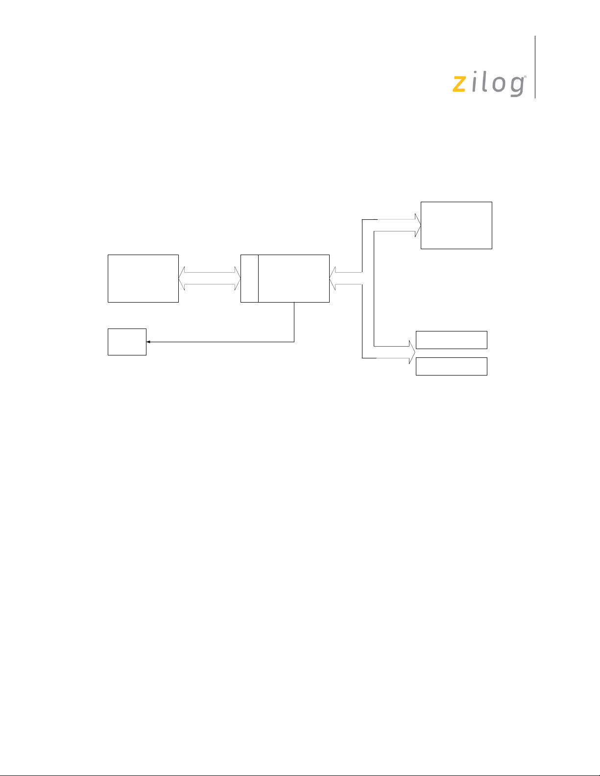
Block Diagram
Figure 1 displays a block diagram of the eZ80F91 Mini Enet Module.
10/100 Ethernet PHY
eZ80F91 Mini Enet Module
Product Specification
3
128KB SRAM
System Bus consists of 24 bits
MII
EMAC
eZ80F91
of address, 8 bits of data, 32
bits of GPIO and control
signals.
System Bus
SIR IrDA
(not installed)
56-Pin Connector J1
56-Pin Connector J2
Figure 1. eZ80F91 Mini Enet Module Functional Block Diagram
PS023603-0907 P R E L I M I N A R Y eZ80F91 Mini Enet Module
Page 8

Pin Description
A21
-HALT_SL
VCC_33V
A14
VCC_33V
A6
GND
A8
A17
D7
GND
A13
-CS2
D1
D0
D3
VCC_33V
-F91_WE
VCC_33V
A19
VCC_SRAM
VCC_SRAM
RTC_VDD
GND
A10
-CS3
A7
GND
A15
A16
A23
A12
-RD
GND
Mini Module Connector J1 – Peripheral Bus
Figure 2 illustrates the pin layout of the 56-pin Peripheral Bus Connector (J1) of the
eZ80F91 Mini Enet Module. The eZ80F91 Mini Enet Module is designed to connect to
your applications via connectors J1 and J2, where the entire system bus and I/O port
signals are available. The module is also compatible with Zilog’s eZ80F91 Modular
Development System (eZ80F910100KIT). Table 1 on page 5 lists the pins and their
functions.
eZ80F91 Mini Enet Module
Product Specification
4
A0
A2
A1
A3
GND
D5
D4
D2
D6
GND
A18
A20
A22
-CS0
GND
-WR
A11
A9
GND
A5
A4
GND
J1
2
4
6
8
10
12
14
16
18
20
22
24
26
28
30
32
34
36
38
P
40
42
44
46
48
50
52
54
56
1
3
5
7
9
11
13
15
17
19
21
23
25
27
29
31
33
35
37
39
41
43
45
47
49
51
53
55
Figure 2. eZ80F91 Mini Enet Module Peripheral Bus Mini Connector Pin Configuration—J1
PS023603-0907 P R E L I M I N A R Y Pin Description
Page 9

Note:
eZ80F91 Mini Enet Module
Product Specification
All signals with an overline are active Low. For example, B/W, for
which WORD is active Low, and B
/W, for which BYTE is active Low.
5
Table 1. eZ80Acclaim! Development Platform Peripheral Bus Connector J1 Identification
Pin No Symbol Signal Direction Active Level eZ80F91 Signal Comments
3 A6 Bidirectional n/a Yes
4 A0 Bidirectional n/a Yes
5 A7 Bidirectional n/a Yes
6 A2 Bidirectional n/a Yes
7 A8 Bidirectional n/a Yes
8 A1 Bidirectional n/a Yes
9 A102 Bidirectional n/a Yes
10 A3 Bidirectional n/a Yes
13 RD
Output Low Yes
14 D5 Bidirectional n/a Yes
15 D1 Bidirectional n/a Yes
16 D4 Bidirectional n/a Yes
17 D0 Bidirectional n/a Yes
1,2
18 D2 Bidirectional n/a Yes
19 A17 Bidirectional n/a Yes
20 D6 Bidirectional n/a Yes
23 A19 Bidirectional n/a Yes
24 A18 Bidirectional n/a Yes
25 A21 Bidirectional n/a Yes
26 A20 Bidirectional n/a Yes
Notes
1. For the sake of simplicity in describing the interface, Power and Ground nets are omitted from this
table. The entire interface is represented in the eZ80F91 Mini Enet Module schematics on pages
16 through 17.
2. Additional note: external capacitive loads on RD
be below 10 pF to satisfy the timing requirements for the eZ80 CPU. All unused inputs should be
pulled to either V
to reduce noise sensitivity. To prevent EMI, the EZ80CLK output can be deactivated via software
in the eZ80F91’s Peripheral Power-Down Register.
PS023603-0907 P R E L I M I N A R Y Pin Description
or GND, depending on their inactive levels to reduce power consumption and
DD
, WR, IORQ, MREQ, D0–D7 and A0–A23 should
Page 10

eZ80F91 Mini Enet Module
Product Specification
6
Table 1. eZ80Acclaim! Development Platform Peripheral Bus Connector J1 Identification
(Continued)
Pin No Symbol Signal Direction Active Level eZ80F91 Signal Comments
27 A23 Bidirectional n/a Yes
28 CS0
29 CS3
33 F91_WE
34 CS0
Output Low Yes
Output Low Yes
Input Low No Jumper on board
Output Low Yes
35 D3 Bidirectional n/a Yes
36 RTC_V
Input n/a Yes
DD
39 D7 Bidirectional n/a Yes
40 HALT_SLP
Output Low Yes
41 A13 Bidirectional n/a Yes
42 WR
Ouput Low Yes
43 A12 Bidirectional n/a Yes
44 A11 Bidirectional n/a Yes
1,2
45 A14 Bidirectional n/a Yes
46 A9 Bidirectional n/a Yes
49 A16 Bidirectional n/a Yes
50 A5 Bidirectional n/a Yes
51 A15 Bidirectional n/a Yes
52 A4 Bidirectional n/a Yes
Notes
1. For the sake of simplicity in describing the interface, Power and Ground nets are omitted from this
table. The entire interface is represented in the eZ80F91 Mini Enet Module schematics on pages
16 through 17.
2. Additional note: external capacitive loads on RD, WR, IORQ, MREQ, D0–D7 and A0–A23 should
be below 10 pF to satisfy the timing requirements for the eZ80 CPU. All unused inputs should be
pulled to either V
to reduce noise sensitivity. To prevent EMI, the EZ80CLK output can be deactivated via software
in the eZ80F91’s Peripheral Power-Down Register.
or GND, depending on their inactive levels to reduce power consumption and
DD
PS023603-0907 P R E L I M I N A R Y Pin Description
Page 11

Mini Module Connector J2 – I/O Ports
eZ80F91 Mini Enet Module
Product Specification
7
Figure 3
Enet Module.
illustrates the pin layout of the
The eZ80F91 Mini Enet Module is
56-pin
I/O Connector (J2) of the eZ80F91 Mini
designed
to connect to your applications
via connectors J1 and J2, where the entire system bus and I/O port signals are available.
The module is also compatible with Zilog’s eZ80F91 Modular Development System
(eZ80F910100KIT). Tab le 2
on page 8 lists the pins and their functions.
J2
PA4
PA5
PA0
PA1
PB7
PC7
PA2
GND
PB0
PC1
PC0
GND
PD7
PD5
PD4
TRIGOUT
GND
PD1
PD0
TDO
GND
IICSCL
IICSDA
-NMI
VCC_33V
10
12
14
16
18
20
22
24
26
28
30
32
34
36
38
40
42
44
46
48
50
52
54
56
2
4
6
8
1
3
5
7
9
11
13
15
17
19
21
23
25
27
29
31
33
35
37
39
41
43
45
47
49
51
53
55
PA3
PA7
PB5
PB6
VCC_33VEZ80CLK
PB1
PC4PB3
PA6
PB4
GND
PB2
PC6PC5
PC3
PC2
GND
TMS
PD6
PD3
-TRSTN
GND
TCK
TDI
PD2
GND
-DIS_IRDA
-WAIT
-RST
VCC_33V
Figure 3. eZ80F91 Mini Enet Module I/O Mini Module Connector Pin Configuration—J2
PS023603-0907 P R E L I M I N A R Y Pin Description
Page 12

eZ80F91 Mini Enet Module
Product Specification
Table 2. eZ80Acclaim! Development Platform/O Mini-Module Connector J2 Identification1
8
Pin No Symbol Signal Direction Active Level eZ80F91 Signal
1 PA3 Bidirectional n/a Yes
2 PA4 Bidirectional n/a Yes
3 PA7 Bidirectional n/a Yes
4 PA5 Bidirectional n/a Yes
5 PB5 Bidirectional n/a Yes
6 PA0 Bidirectional n/a Yes
7 PB6 Bidirectional n/a Yes
8 PA1 Bidirectional n/a Yes
10 EZ80CLK Output n/a Yes
11 PB1 Bidirectional n/a Yes
12 PB7 Bidirectional n/a Yes
13 PC4 Bidirectional n/a Yes
14 PB3 Bidirectional n/a Yes
15 PA6 Bidirectional n/a Yes
16 PC7 Bidirectional n/a Yes
2
17 PB4 Bidirectional n/a Yes
18 PA2 Bidirectional n/a Yes
21 PB3 Bidirectional n/a Yes
22 PB0 Bidirectional n/a Yes
23 PC6 Bidirectional n/a Yes
24 PC5 Bidirectional n/a Yes
25 PC3 Bidirectional n/a Yes
26 PC1 Bidirectional n/a Yes
27 PC2 Bidirectional n/a Yes
28 PC0 Bidirectional n/a Yes
Notes
1. For the sake of simplicity in describing the interface, Power and Ground nets are omitted
from this table. The entire interface is represented in the eZ80F91 Mini Enet Module schematics on pages 16 through 17.
2. The Power and Ground nets are connected directly to the eZ80F91 device.
PS023603-0907 P R E L I M I N A R Y Pin Description
Page 13

eZ80F91 Mini Enet Module
Product Specification
9
Table 2. eZ80Acclaim! Development Platform/O Mini-Module Connector J2 Identification
(Continued)
Pin No Symbol Signal Direction Active Level eZ80F91 Signal
2
31 TMS Input n/a Yes
32 PD7 Bidirectional n/a Yes
33 PD6 Bidirectional n/a Yes
34 PD5 Bidirectional n/a Yes
35 PD3 Bidirectional n/a Yes
36 PD4 Bidirectional n/a Yes
37 TRSTN
Input Low Yes
38 TRIGOUT Output n/a Yes
41 TCK Input n/a Yes
42 PD1 Bidirectional n/a Yes
43 TDI Bidirectional n/a Yes
44 PD0 Bidirectional n/a Yes
45 PD2 Bidirectional n/a Yes
1
46 TDO Output n/a Yes
49 DIS_IRDA
Input Low No
50 IICSCL I/O n/a Yes
51 WAIT
Input Low Yes
52 IICSDA I/O n/a Yes
53 RST
54 NMI
Notes
1. For the sake of simplicity in describing the interface, Power and Ground nets are omitted
from this table. The entire interface is represented in the eZ80F91 Mini Enet Module schematics on pages 16 through 17.
2. The Power and Ground nets are connected directly to the eZ80F91 device.
I/O Low Yes
Input Low Yes
PS023603-0907 P R E L I M I N A R Y Pin Description
Page 14

eZ80F91 Mini Enet Module
Product Specification
Onboard Component Description
I/O Connector
The I/O connector features 32 general-purpose 3.3 V CMOS I/O pins that can be used as
outputs or inputs interfacing to external logic. All I/Os are 5 V tolerant. Some of the
general-purpose I/O pins support dual mode functions (SPI, Timer I/O, UARTs and bit I/O
with edge- or level-triggered interrupt functions on each pin). For more information on
eZ80F91 dual modes, refer to
Peripheral Bus Connector
eZ80F91 Product
Specification (PS0192)
10
.
The peripheral bus connector features 24-pins that provide access to the eZ80F91 Mini
Enet Module address bus and 8-pins that provide access to the module data bus. For more
information on eZ80F91 address and data buses, refer to eZ80F91 Product Specification
(PS0192).
Ethernet PHY and RJ45 Connector
The eZ80F92 Ethernet Module contains a Micrel KS8721BL 10/100 Ethernet PHY with
Media Independent Interface (MII) and a HALO RJ45 with integrated magnetics and two
LEDs (transformer and common-mode chokes).
The eZ80F92 Ethernet Module defaults to 10 Mbps, which works in either a 100 Mbps or
a 10 Mbps network. Software can also configure the PHY for 100 Mbps or autosense.
Ethernet LEDs
The Ethernet connection is provided by the HALO RJ45 connector. It contains two green
LEDs that are located next to each other on the eZ80F91 Mini Enet Module. When PHY is
receiving data, the left LED is on. When the PHY is transmitting data, the right LED is on.
5 MHz Clock
The eZ80F91 Mini Enet Module contains a 5 MHz crystal oscillator (Y2) which is
multiplied by the phase-locked loop in the eZ80F91 MCU to create a 50 MHz system
clock
PS023603-0907 P R E L I M I N A R Y Onboard Component Description
Page 15

Memory
The eZ80F91 MCU contains 256 KB of internal Flash memory. Additional memory can
be accommodated via the system bus on connectors J1 and J2. To program the on-chip
Flash memory, install jumper JP1 on the mini module. Table 3 lists the status of the
jumper.
Table 3. Shunt JP1, eZ80F91 Mini Enet Module
Shunt
Symbol Jumper Name
Status Function Affected Device
eZ80F91 Mini Enet Module
Product Specification
11
JP1 F91_WE
There is 128 KB of fast SRAM on the eZ80F91 Mini Enet Module. Access time is 12 ns,
which requires one wait-state access. The eZ80F91 on-chip SRAM can be used with zero
wait states.
IrDA Transceiver
The eZ80F91 Mini Enet Module is shipped without an IrDA transceiver installed.
If you install an on-board transceiver, such as the Zilog ZHX1810, it is connected to PD0
(TX), PD1 (RX), and PD2 (Shutdown, IR_SD). The IrDA transceiver is of the LED type
870 nm Class 1.
The IrDA transceiver is accessible via the IrDA controller attached to UART0 on the
eZ80F91 device.
To use the UART0 for console or to save power, the transceiver is disabled by the software
or by an off-board signal when using the proper jumper selection. The transceiver is
disabled by setting PD2 (IR_SD) High or by pulling the DIS_IRDA
connector Low. The shutdown is used for power savings. To enable the IrDA transceiver,
DIS_IRDA
In (Default) On-chip Flash is enabled for
writing to boot block.
Out On-chip Flash memory boot block
is write-protected.
is left floating and PD2 is set to Low.
On-chip Flash
On-chip Flash
pin on the I/O
PS023603-0907 P R E L I M I N A R Y Onboard Component Description
Page 16

Serial Interface Ports
The eZ80F91 MCU contains two UARTs with programmable baud rate generators.
UART0 is connected to GPIO PD[0:7] on the I/O connector. UART1 is connected to
GPIO PC[0:7] on the I/O connector.
eZ80F91 Mini Enet Module
Product Specification
12
Note:
Do not connect an RS232 interface without level shifters. There are
no RS232-level shifters on the eZ80F91 Mini Enet Module.
Physical Dimensions
The footprint of the eZ80F91 Mini Enet Module PCB is 2.00 " x 1.90 ". See Figure 4 for
dimensions and top-layer silkscreen.
Figure 4. Physical Dimensions of the eZ80F91 Mini Enet Module
PS023603-0907 P R E L I M I N A R Y Onboard Component Description
Page 17

eZ80F91 Mini Enet Module
Absolute Maximum Ratings
The stress greater than those listed in Tabl e 4 can cause permanent damage to the device.
These ratings are stress ratings only. Operation of the device at any condition outside those
indicated in the operational sections of these specifications is not implied. Exposure to
absolute maximum rating conditions for extended periods may affect device reliability.
For improved reliability, unused inputs should be tied to one of the supply voltages (V
or V
Table 4. Absolute Maximum Ratings
Parameter Minimum Maximum Units
Standard operating temperature
Storage temperature
Operating Humidity (RH @ 50ºC)
Operating Voltage
SS
).
0+70ºC
–45 +85 ºC
25% 90%
—3.6V
Product Specification
DD
13
PS023603-0907 P R E L I M I N A R Y Onboard Component Description
Page 18

Module Bill of Materials
Table 5 lists the installed components of the eZ80F91 Mini Enet Module.
Table 5. Bill of Materials for the eZ80F91 Mini Enet Module,
ITEM PART NUMBER DESCRIPTION QTY LOCATION
1 98C0942-001 FAB,eZ80F91 ETHERNET MODULE, REV B 1
Coastal Circuits
2 35-0016-06 IC,74LVC3G04,3.3V,GATE,8-SSOP 1 U1
TEXAS INSTR SN74LVC3G04DCTR
3 35-0179-12 IC,SRAM,128Kx8,12ns,3V,32-SOJ 1 U3
IDT IDT71V124SA12Y
4 35-0062-03 IC,74AHC1G32,SNGL QUAD OR,SOR23-5 1 U4
TEXAS INSTR SN74AHC1G32DBVR
5 35-0022-02 IC,KS8721BL,PHY XCVR,48-LQFP 1 U5
MICREL SEMI KS8721BL
6 EZ80F91 IC,eZ80F91,50MHZ,144BGA 1 U6
ZiLOG EZ80F91NA050SC
7 17-2005-83 CAP,0.33UF,16V,CER CHIP,0603 1 C1
PANASONIC ECJ-1VF1C334Z
8 17-2005-70 CAP,1,000PF,50V,CER CHIP,0603 11 C2,C18,C25-33
PANASONIC ECJ-1VC1H561J
9 17-2005-66 CAP,0.1UF,16V,CER CHIP,0603 14 C3,C7,C9,C13-17,
KEMET C0603C104K5RAC C21,C24,C38-41
10 17-2001-05 CAP,22PF,50V,CER CHIP,0603 4 C5,C6,C51,C52
PANASONIC ECJ-1VC1H220J
11 17-0018-20 CAP,10UF,25V,TANT CHIP,SMT 2 C8,C10
PANASONIC ECSH1ED106R
12 17-2005-63 CAP,0.056UF,50V,CER CHIP,0603 1 C11
PANASONIC ECJ-1VB1C563K
13 17-2001-20 CAP,270PF,50V,CER CHIP,0603 1 C12
PANASONIC ECJ-1VC1H271J
14 17-0018-47 CAP,47UF,16,TANT CHIP,SMT 2 C19,C20
PANASONIC ECS-T1CD476R
15 17-2001-04 CAP,18PF,50V,CER CHIP,0603 2 C22,C23
PANASONIC ECJ-1VC1H180J
16 17-9009-10 FERRITE BEAD,3AMP,100 OHM,1206 SMT 2 FB1,FB2
STEWARD HI1206N101R-00
17 46-3001-03 RES,10K OHM,1%,1/16W,0603 SMT 6 R1,R7-9,R11,R12
18 46-3000-79 RES,4.75K OHM,1%,1/16W,0603 SMT 3 R2,R3,R26
19 46-3000-35 RES,68 OHM,1%,1/16W,0603 SMT 1 R4
20 46-3000-02 RES,2.2 OHM,1%,1/16W,0603 SMT 1 R5
21 46-3000-71 RES,2.21K OHM,1%,1/16W,0603 SMT 1 R6
22 46-3000-83 RES,6.81K OHM,1%,1/16W,0603 SMT 1 R13
23 46-3000-63 RES,1K OHM,1%,1/16W,0603 SMT 2 R15,R16
24 46-3000-56 RES,499 OHM,1%,1/16W,0603 SMT 1 R18
25 46-3000-27 RES,33.2 OHM,1%,1/16W,0603 SMT 1 R19
26 46-3000-32 RES,49.9 OHM,1%,1/16W,0603 SMT 4 R20,R21,R22,R25
27 46-3000-47 RES,221 OHM,1%,1/16W,0603 SMT 2 R23,R24
28 46-3001-27 RES,100K OHM,1%,1/16W,0603 SMT 1 R27
29 23-0006-25 XTAL,25.0000MHZ,18PF,CYL 1 Y1
EPSON CA-301 25.0000M-C
eZ80F91 Mini Enet Module
Product Specification
14
PS023603-0907 P R E L I M I N A R Y Onboard Component Description
Page 19

Table 5. Bill of Materials for the eZ80F91 Mini Enet Module (Continued)
ITEM PART NUMBER DESCRIPTION QTY LOCATION
30 23-0000-05 XTAL,5.0000MHZ,SER/RESN,HC49US 1 Y2
CITIZEN HC49US5.000MABJ
31 23-0006-00 XTAL,32.768KHZ,SER/RESN,TF CASE 1 Y3
FOX NC38-32.768KHZ OR ECS ECS-3X8
32 21-8010-56 CONN,56-CKT,.8mm,HDR/PIN 2 J1,J2
SAMTEC FTE-128-01-G-DV-A
33 21-0055-01 CONN,HDR/PIN,.025SQ,SNGL ROW 0.1 JP1
HARWIN M-20-977-3622
34 21-0907-01 CONN,RJ45,FASTJACK,10/100BASE-T 1 P1
HALO ELECTRONICS HFJ11-2450E-L11
35 21-0192-00 SHUNT,2-POS,.1 CNTR,LOW PRFL 1 JP1
AMP 382811-5
eZ80F91 Mini Enet Module
Product Specification
15
PS023603-0907 P R E L I M I N A R Y Onboard Component Description
Page 20

e
Z80F91 Mini Enet Modul
y
[
]
]
[
]
]
[
]
[
]
[
]
]
]
]
]
]
]
]
Product Specification
e
Schematics
Figures 5 and 6 describe the layout of the eZ80F91 Mini Enet Module. Ethernet circuiting devices are not loaded on the
eZ80F91 Mini Enet Module. However, these devices appear in the following schematics for reference purposes.
5
VCC_33V
A[0..23
A[0:23
D
-RD
-WR
-WAIT
-NMI
TRIGOUT
RTC_VDD
-RST
TDI
TCK
TMS
TDO
-TRSTN
GND
0..7
-CS
0..3
IICSDA
IICSCL
-HALT_SLP
eZ80CLK
PA
0..7
PB[0..7
0..7
PC
PD
0..7
-RD
-WR
-WAIT
-NMI
TRIGOUT
-TRSTN
VCC_33V
VCC_33V
GND
5
D[0:7
-HALT_SLP
RTC_VDD
VCC_33V
GND
-CS[0:3
IICSDA
IICSCL
eZ80CLK
PA[0:7
PB[0:7
PC[0:7
PD[0:7
-RST
D D
C C
B B
A A
TMS
TDO
R2
4.7K
2.2K
10K
VCC_33V
R8
R3
4.7K
IICSDA
IICSCL
R7
R6
10K
R9
10K
TDI
TCK
4
VCC_33V
A0
A2
A1
A3
GND
D5
D4
D2
D6
GND
A18
A20
A22
-CS0
VCC_33V
-CS2
RTC_VDD
GND
-HALT_SLP
-WR
A11
A9
GND
A5
A4
GND
-DIS_IRDA
4
J1
2
4
6
8
10
12
14
16
18
20
22
24
26
28
30
32
34
36
38
40
42
44
46
48
50
52
54
56
HEADER 28x2
VCC_33V
R11
10K
VCC_33V
1
A6
3
A7
5
A8
7
A10
9
GND
11
-RD
13
D1
15
D0
17
A17
19
GND
21
A19
23
A21
25
A23
27
-CS3
29
VCC_33V
31
-F91_WE
33
D3
35
GND
37
D7
39
A13
41
A12
43
A14
45
GND
47
A16
49
A15
51
GND
53
VCC_SRAMVCC_SRAM
55
U1A
1 7
SN74LVC2G04
4 8
VCC_33V
PD2
=
GND
IR_SD
1
2
3
connector 2connector 1
PA4
PA5
PA0
PA1
PB7
PC7
PA2
GND
PB0
PC1
PC0
GND
PD7
PD5
PD4
TRIGOUT
GND
PD1
PD0
TDO
GND
IICSCL
IICSDA
-NMI
VCC_33V
53
SN74AHC1G32
3
A0
A2
A1
A3
A11
A9
A5
A4
A15
A16
A14
A12
A13
A10
A8
A7
A6
-WR
-RD
-CS1
2
4
6
8
10
12
14
16
18
20
22
24
26
28
30
32
34
36
38
40
42
44
46
48
50
52
54
56
U4
4
J2
1
3
5
7
9
11
13
15
17
19
21
23
25
27
29
31
33
35
37
39
41
43
45
47
49
51
53
55
HEADER 28x2
U3
1
A0
2
A1
3
A2
4
A3
13
A4
14
A5
15
A6
16
A7
17
A8
18
A9
19
A10
20
A11
21
A12
29
A13
30
A14
31
A15
32
A16
12
WE
28
OE
5
CS
IDT71V124S/SO
IRDA_SD
PA3
PA7
PB5
PB6
VCC_33VEZ80CLK
PB1
PC4PB3
PA6
PB4
GND
PB2
PC6PC5
PC3
PC2
GND
TMS
PD6
PD3
-TRSTN
GND
TCK
TDI
PD2
GND
-DIS_IRDA
-WAIT
-RST
VCC_33V
I/O0
I/O1
I/O2
I/O3
I/O4
I/O5
I/O6
I/O7
VCC
VCC
GND
GND
2
GND
-F91_WE
1
2
HEADER 2
JP1
-F91_WE
D5
6
D4
7
D2
10
D6
11
D7
22
D3
23
D0
26
D1
27
VCC_SRAM
24
8
C3
C2
0.1uF
25
9
0.001uF
GND
U1B
3 5
R1
SN74LVC2G04
10K
VCC_33v
R5
2R7
(MMA 0204)
PD0
IRDA_SD
PD1
U1C
6 2
SN74LVC2G04
R4
68R
-F91_WP
5
1
2
4
3
6
C1
330nF
U2
VCC
LEDA
TXD
SD
RXD
GND
1
-F91_WP
T
0
ZHX1810
CONNECTORS
ZiLOG, Inc.
532 Race Street. San Jose,CA 95126. 408.558.8500
Title
eZ80F91 Ethernet Mini Module.
Size Document Number Rev
B
2
Date: Sheet of
96C0942-001 B
, April 07, 2004
1
12Wednesda
16
Figure 5. eZ80F91 Mini Enet Module Schematic Diagram, #1 of 2—Connectors and Miscellaneous
PS023603-0907 PRELIMINARY Schematics
Page 21

e
Z80F91 Mini Enet Modul
y
]
]
]
]
]
]D[
]
p
p
p
p
p
p
p
Product Specification
e
17
5
0:7
F
C23
18
-F91_WP
F
RTC_VDD
Y3
32.768KHz
C51
22
F
GND
5
R18
499
-WAIT
-NMI
TMS
TCK
TDI
-RST
R19
33
-BUSREQ
-TRSTN
-RST
-F91_WP
FILT_IN
XIN
XOUT_O
VCC_33V
C52
22
D D
C C
B B
A A
R12
VCC_33V VDDC
10K
-TRSTN
C11
GND
0.056uF
C12
270
Y2
5MHz
R27
100K
C22
18
F
RTC_VDD
U6
D0
L2
D1
D2
D3
D4
D5
D6 A6
D7
-WAIT
-NMI
TMS
TCK
TDI
CRS
COL
RXER
RXDV
RXD3
RXD2
RXD1
RXD0
RXCLK
TXCLK
D0
K3
D1
J4
D2
M3
D3
L3
D4
H5
D5
L4
D6
M4
D7
L6
WAIT
M7
BUSREQ
J6
NMI
H7
TMS
L9
TCK
K9
TDI
L10
TRSTN
K6
RESET
A2
WP
D8
MII_CRS
A7
MII_COL
D6
MII_RXER
A4
MII_RXDV
C4
MII_RXD3
D5
MII_RXD2
B4
MII_RXD1
E6
MII_RXD0
C5
MII_RXCLK
C6
MII_TXCLK
J10
FILT_IN
H11
XIN
H12
XOUT
H10
PLL_VDD
A5
VDD
B8
VDD
C1
VDD
C10
VDD
E2
VDD
E11
VDD
G2
VDD
H9
VDD
J2
VDD
J11
VDD
K4
VDD
K7
VDD
M1
VDD
G7
PLL_VSS
B5
VSS
B12
VSS
C2
VSS
C8
VSS
D9
VSS
E3
VSS
F9
VSS
G3
VSS
G6
VSS
G12
VSS
H4
VSS
H6
VSS
J12
VSS
K8
VSS
M2
VSS
M11
VSS
J7
RTC_VDD
L8
RTC_XOUT
M8
RTC_XIN
F
eZ80F91_BGA
PA6_PWM2_EC1
PA5_PWM1_TOUT1
PA4_PWM0_TOUT0
PA3_PWM3_OC3
PA2_PWM2_OC2
PA1_PWM1_OC1
PA0_PWM0_OC0
PD1_RXD0_IRRXD
PD0_TXD0_IRTXD
A0
A1
A2
A3
A4
A5
A6
A7
A8
A9
A10
A11
A12
A13
A14
A15
A16
A17
A18
A19
A20
A21
A22
A23
MII_TXD3
MII_TXD2
MII_TXD1
MII_TXD0
MII_TXEN
MII_TXER
MII_MDC
MII_MDIO
IORQ
MRQ
RD
WR
BUSACK
CS0
CS1
CS2
CS3
SCL
SDA
PA7_PWM3
PB7_MOSI
PB6_MISO
PB5_ICB3
PB4_ICA2
PB3_SCK
PB2_SS
PB1_IC1
PB0_IC0_EC0
PC7_RI1
PC6_DCD1
PC5_DSR1
PC4_DTR1
PC3_CTS1
PC2_RTS1
PC1_RXD1
PC0_TXD1
PD7_RI0
PD6_DCD0
PD5_DSR0
PD4_DTR0
PD3_CTS0
PD2_RTS0
HALT_SLP
PHI
INSTRD
TDO
TRIGOUT
4
A0
A1
A1
B1
A2
B2
A3
C3
A4
D4
A5
E5
D2
A7
D1
A8
D3
A9
F6
A10
E1
A11
E4
A12
F1
A13
F2
A14
F3
A15
F4
A16
G1
A17
F5
A18
H1
A19
H2
A20
G4
A21
H3
A22
J1
A23
G5
TXD3
B7
TXD2
C7
TXD1
D7
TXD0
A6
TXEN
B6
TXER
E7
MDC
A3
MDI0
B3
M5
L5
-RD
K5
-WR
J5
L7
-CS0
J3
-CS1
K1
-CS2
K2
-CS3
L1
SCL
A11
SDA
A12
PA7
A8
PA6
F7
PA5
C9
PA4
A9
PA3
B9
PA2
E8
PA1
B10
PA0
A10
PB7
C11
PB6
C12
PB5
D10
PB4
E9
PB3
D11
PB2
F8
PB1
D12
PB0
E10
PC7
E12
PC6
G8
PC5
F10
PC4
F11
PC3
F12
PC2
G9
PC1
G10
PC0
G11
PD7
H8
PD6
K11
PD5
K12
PD4
J9
PD3
K10
PD2
L11
PD1
L12
PD0
M12
M9
B11
M6
M10
J8
4
-RD
-WR
IICSCL
IICSDA
A[0:23
-CS[0:3
PA[0:7
PB[0:7
PC[0:7
PD[0:7
-HALT_SLP
eZ80CLK
TDO
TRIGOUT
VCC_33V
C13
0.1uF
R26
4.7K
C25
0.001uF
C38
0.1uF
VCC_33V
VDDC
C14
0.1uF
GND
GND
3
VDDC
C26
0.001uF
C39
0.1uF
VCC_33V
3
MDI0
MDC
RXD3
RXD2
RXD1
RXD0
VCC_33V
RXDV
RXCLK
RXER
TXER
TXCLK
TXEN
TXD0
TXD1
TXD2
TXD3
COL
CRS
VCC_33V
GND
U5
1
MDIO
2
MDC
3
RXD3/PHYAD1
4
RXD2/PHYAD2
5
RXD1/PHYAD3
6
RXD0/PHYAD4
7
VCC
GND
8
GND
9
RXDV/PCS_LPBK
10
RXC
11
RXER/ISO
GND
12
GND
13
VDDC
14
TXER
15
TXC/REFCLK
16
TXEN
17
TXD0
18
TXD1
19
TXD2
20
TXD3
21
COL/RMII
22
CRS/RMII_BTB
GND
23
GND
24 25
VCC INT/PHYADD0
C16
C15
0.1uF
0.1uF
C27
0.001uF
C40
0.1uF
VCC_33V
GND
+
C28
0.001uF
C41
0.1uF
C19
47uF
KS8721BL
RST
VDDPLL
XO
GND
GND
VDDTX
TX+
TX-
GND
VDDRCV
REXT
GND
GND
FXSD/FXEN
RX+
RX-
VDDRX
PD
LED3/NWAYEN
LED2/DUPLEX
LED1/SPD100/noFEF
LED0/TEST
C29
C30
0.001uF
0.001uF
CPU & PHY
48
47
46
XI
45
44
43
42
41
40
39
38
37
36
35
34
33
32
31
30
29
28
27
26
VCC_33V
2
C17
0.1uF
GND
VCC_33V
R23
220
C31
0.001uF
2
-RST
VDD_PLL
GND
GND
GND
RX+
RX-
-SPEED
-LEDLNK
22
F
F
22
C9
0.1uF
R15
1K
VCC_33V
1
GND
+
1
C10
10uF
1 2
VCC_33V
1
4
2
3
5
6
8
9
10
11
12
22Wednesda
C5
Y1
25 MHz
C6
TX+
R13 6.81K 1%
TX-
GND
GND
C7
0.1uF
INT
1
Header 1
JP2
+
C20
C18
47uF
0.001uF
R20
49.9
R22 49.9
R21 49.9
R24
220
R25 49.9
VCC_33V
C32
C33
0.001uF
0.001uF
GND
ZiLOG, Inc.
532 Race Street. San Jose,CA 95126. 408.558.8500
Title
eZ8 0F91 Ethernet Mini Module.
Size Document Number Rev
B
Date: Sheet of
FB1
1 2
Ferrite Bead
+
C8
10uF
GND
Make sure that power connections
and nets VDD_PLL and VDDC have
the shortest route possible
R16 1K
TX+
TX-
RX+
RX-
C24
0.1uF
-LEDLNK
-SPEED
96C0942-001 B
, April 07, 2004
FB2
Ferrite Bead
C21
0.1uF
P1
TX+
TXCT
TX-
RX+
RXCT
RX-
GND
AN1
CT1
AN2
CT2
HFJ11-2450E
VCC_33V
Figure 6.eZ80F91 Mini Enet Module Schematic Diagram, #2 of 2—CPU and PHY
PS023603-0907 PRELIMINARY Schematics
Page 22

Customer Support
For answers to technical questions about the product, documentation, or any other issues
with Zilog’s offerings, please visit Zilog’s Knowledge Base at
http://www.zilog.com/kb
For any comments, detail technical questions, or reporting problems, please visit Zilog’s
Technical Support at http://support.zilog.com
.
eZ80F91 Mini Enet Module
Product Specification
18
.
PS023603-0907 P R E L I M I N A R Y Customer Support
 Loading...