

Page 1

Digital Jitter Meter
IM 704610-01E
3rd Edition
Page 2

Product Registration
Thank you for purchasing YOKOGAWA products.
YOKOGAWA provides registered users with a variety of information and
services.
Please allow us to serve you best by completing the product registration
form accessible from our homepage.
http://www.yokogawa.com/tm/
PIM 103-01E
Page 3

Foreword
Notes
Thank you for purchasing the YOKOGAWA TA220 Digital Jitter Meter. This user’s
manual contains useful information about the functions and operating procedures of the
instrument as well as precautions that should be observed during use. To ensure proper
use of the instrument, please read this manual thoroughly before beginning operation.
After reading this manual, keep it in a convenient location for quick reference in the event
a question arises.
There are two manuals for the TA220 including this one. If the option function is installed,
please read both manuals.
Manual Title Manual No. Description
TA220 Digital Jitter Meter IM 704610-01E This manual. Explains all functions and
User’s Manual operating procedures of the TA220
excluding the option function.
TA220 Digital Jitter Meter IM 704610-51E Explains the operating procedures of
Option Function User’s Manual the TA220 option function.
• The contents of this manual are subject to change without prior notice as a result of
improvements in the instrument’s performance and functions. Display contents
illustrated in this manual may differ slightly from what actually appears on your screen.
• Every effort has been made in the preparation of this manual to ensure the accuracy
of its contents. However, should you have any questions or find any errors, please
contact your nearest YOKOGAWA representative as listed on the back cover of this
manual.
• Copying or reproduction of all or any part of the contents of this manual without the
permission of Yokogawa Electric Corporation is strictly prohibited.
• The TCP/IP software or TCP/IP related documentation used for this software was
developed or created using BSD Networking Software, Release 1 licensed from the
Regents of the University of California at Berkeley.
Trademarks
• Adobe, Acrobat, and Acrobat Reader are either trademarks or registered trademarks
of Adobe Systems in the United States and/or other countries.
• The company and product names used in this manual are not accompanied by the
trademark or registered trademark symbols (™ and ®).
• Other company and product names are trademarks or registered trademarks of their
respective companies.
Revisions
1st Edition: July 2004
2nd Edition: January 2005
3rd Edition: October 2007
3rd Edition : October 2007 (YK)
All Rights Reserved, Copyright © 2004 Yokogawa Electric Corporation
IM 704610-01E
i
Page 4
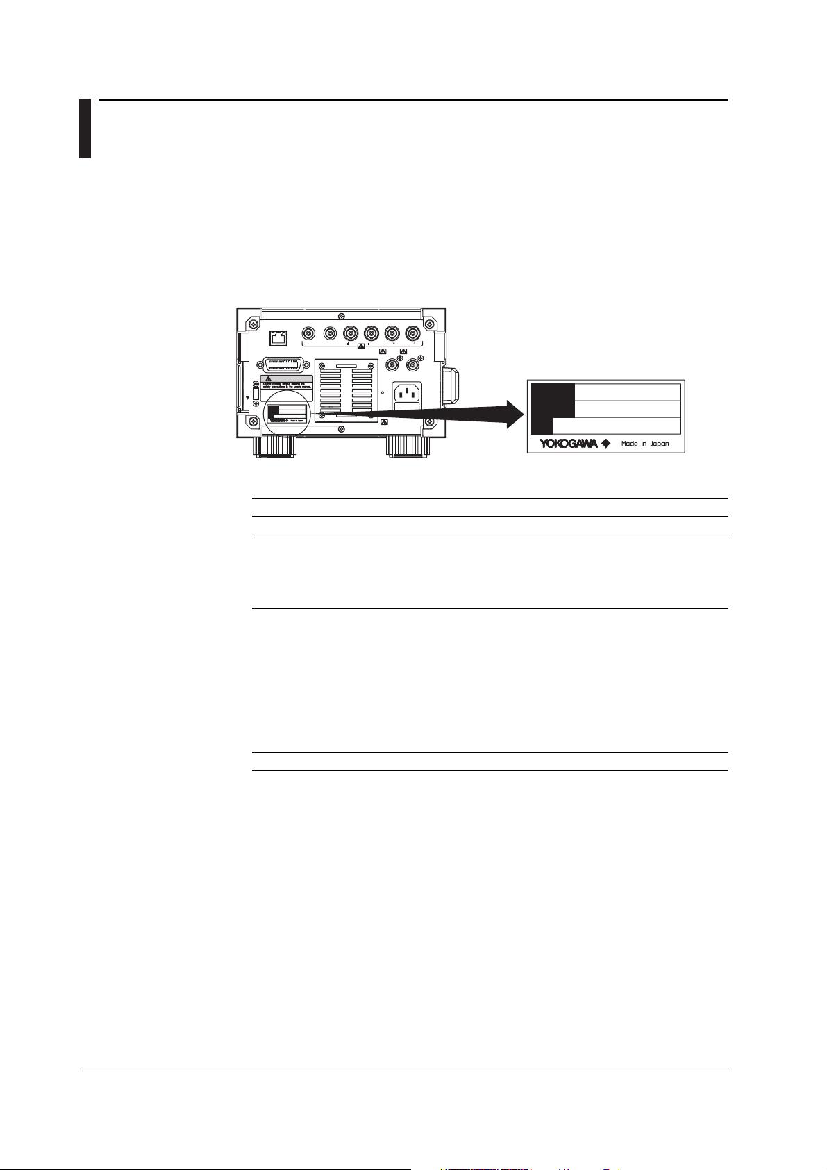
Checking the Contents of the Package
Unpack the box and check the contents before operating the instrument. If some items
are missing or otherwise inconsistent with the contents description, please contact your
dealer or nearest YOKOGAWA representative.
TA220
Check that the model name and suffix code given on the name plate on the rear panel
match the ones you ordered.
CLOCK
OUT
( 0.4V)
EQUALIZED
MONITOR
OUT
OUT
(50 )
JITTER LEVEL
DC OUT DC OUT
(0 to +5V) (0 to +5V)
MODEL
100-120V/200-240V AC
100VA MAX 50/60Hz
FUSE 250V T 5A
SUFFIX
NO.
(the -BDS equalizer specification will be discontinued in
December, 2004, upon release of -BD1).
D-to-C jitter measurement excluding 2T
[Maximum rated voltage: 125 V; Maximum rated current: 7 A]
[Maximum rated voltage: 250 V; Maximum rated current: 10 A]
[Maximum rated voltage: 250 V; Maximum rated current: 10 A]
[Maximum rated voltage: 240 V; Maximum rated current: 10 A]
[Maximum rated voltage: 250 V; Maximum rated current: 10 A]
EXT ARM
ETHERNET
IN
100BASE-TX
ACT
LINK
GP-IB(IEEE488)
WARNING
KEY
LOCK
MODEL
SUFFIX
NO.
SLICED RF
INHIBIT
OUT
IN
(TTL) (TTL) ( 0.4V) (50 )
Model and Suffix Code
Model Suffix Specification
704610 100–120 VAC, 200-240 VAC
Equalizer -BDS Conventional equalizer for BD
-BD1 Conventional equalizer for BD, D-to-C high speed calculation,
Power cord -D UL/CSA standard power cord (Part No.: A1006WD)
-F VDE standard power cord (Part No.: A1009WD)
-Q BS standard power cord (Part No.: A1054WD)
-R AS standard power cord (Part No.: A1024WD)
-H GB standard power cord (Part No.: A1064WD)
Option* /LEQ Limit equalizer for BD
* For information on the option, see the TA220 Digital Jitter Meter Option Function User’s
Manual (IM 704610-51E). Also, the option cannot be selected for products with suffix code BDS.
NO. (Instrument Number)
When contacting the dealer from which you purchased the instrument, please give them
the instrument number.
ii IM 704610-01E
Page 5
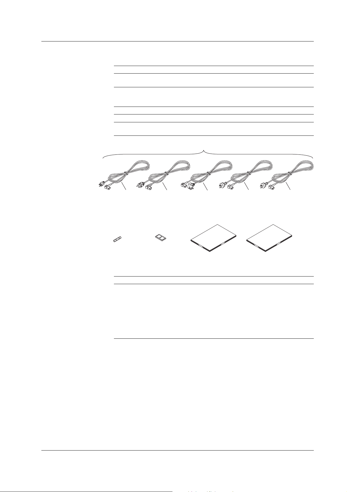
Standard Accessories
The following accessories are included in the package.
Power cord (One of the following power cords is supplied according to the suffix codes.)
Checking the Contents of the Package
Part Name Model/Part Number Qty. Notes
Power cord One of the following power cords is included according to the
suffix code on the previous page.
Spare fuse for power supply A1114EF 1 250 V, 5 A, time lag
Installed in the main unit fuse
holder
Rubber feet A9088ZM 2 Two rubber feet in one set
User’s manual IM704610-01E 1 This manual
Option function user’s manual IM704610-51E 1 Included for instruments with
the option installed
D
Spare fuse for
power supply
A1114EF
1 piece
Rubber feet
A9088ZM
2 sheets
Optional Accessories (Sold Separately)
The following optional accessories are also available.
Name Model Lot Qty. Description
Power fuse A1114EF 2 250 V, 5 A, time lag
150-MHz probe 700998 1 Input resistance: 10 MΩ, length: 1.5 m (10:1
BNC cable 366924 1 BNC-BNC, length: 1m
BNC cable 366925 1 BNC-BNC, length: 2 m
Rack mount kit 751533-E3 1 For EIA single mount
Rack mount kit 751534-E3 1 For EIA dual mount
Rack mount kit 751533-J3 1 For JIS single mount
Rack mount kit 751534-J3 1 For JIS dual mount
F
Q
User’s manual
IM704610-01E
and 1:1 switching type)
R
Option function
user’s manual
IM704610-51E
H
IM 704610-01E
iii
Page 6

Safety Precautions
This instrument is an IEC safety class I instrument (provided with terminal for protective
earth grounding). The following general safety precautions must be taken during all
phases of operation, service, and repair of this instrument. If the instrument is used in a
manner not specified in this manual, the protection provided by the instrument may be
impaired. YOKOGAWA Electric Corporation assumes no liability for the customer’s
failure to comply with these requirements.
The instrument is marked with the following symbols.
Danger. Refer to the user’s manual. This symbol appears on dangerous
locations on the instrument which require special instructions for proper handling
or use. The same symbol appears in the corresponding place in the manual to
identify those instructions.
Alternating current
ON (power)
OFF (power)
In-position of a bistable push control
Out-position of a bistable push control
iv IM 704610-01E
Page 7

Safety Precautions
Make sure to take the following precautions. Failure to take these precautions might
result in injury or death of personnel.
WARNING
• Use the Correct Power Supply
Before connecting the power cord, ensure that the source voltage matches the
rated supply voltage of the instrument and that it is within the maximum rated
voltage of the provided power cord.
• Use the Correct Power Cord and Plug
To prevent the possibility of electric shock or fire, be sure to use the power cord
supplied by YOKOGAWA. The main power plug can only be plugged into an
outlet with a protective grounding terminal. Do not disable the protection feature
of the instrument by using an extension cord without protective grounding.
• Connect the Protective Grounding
Make sure to connect the protective grounding to prevent electric shock before
turning ON the power. The power cord included with this instrument is a 3-prong
cord with a grounding wire. Connect the power cord to a 3-prong AC outlet with
a protective grounding terminal.
• Do Not Impair the Protective Grounding
Never cut off the internal or external protective grounding wire or disconnect the
wiring from the protective grounding terminal. Doing so creates a potential shock
hazard.
• Do Not Operate with Defective Protective Grounding or Fuse
Never operate the instrument if you suspect the protective grounding or fuse
might be defective. Make sure to check them before operation.
• Use the Correct Fuse
To prevent fire, make sure to use fuses of the specified rating for voltage,
current, and type. Make sure to turn OFF the instrument and unplug the power
cord before replacing the fuse. Never short the fuse holder.
• Do Not Operate Near Flammable Materials
Do not operate the instrument in the presence of flammable liquids or vapors.
Operation of any electrical instrument in such an environment constitutes a
safety hazard.
• Do Not Use When Removed from the Case
The cover should be removed by qualified personnel only. There are some
areas inside the instrument with high voltages.
• Ground the Instrument before Making External Connections
Connect the protective grounding before connecting to the item under
measurement or external control circuits. Also, If you need to touch the circuit
with your hand, first cut the power to the circuit and confirm that it contains no
voltage. To prevent the possibility of electric shock or an accident, connect the
ground of the probe and input connector to the ground of the item being
measured.
See below for operating environment limitations.
This product is a Class A (for industrial environments) product. Operation of this
product in a residential area may cause radio interference in which case the user
will be required to correct the interference.
IM 704610-01E
CAUTION
v
Page 8

Waste Electrical and Electronic Equipment
Waste Electrical and Electronic Equipment (WEEE), Directive 2002/96/EC
(This directive is only valid in the EU.)
This product complies with the WEEE Directive (2002/96/EC) marking
requirement. This marking indicates that you must not discard this electrical/
electronic product in domestic household waste.
Product Category
With reference to the equipment types in the WEEE directive Annex 1, this
product is classified as a ÅgMonitoring and Control instrumentationÅh product.
Do not dispose in domestic household waste. When disposing products in the
EU, contact your local Yokogawa Europe B. V. office.
vi IM 704610-01E
Page 9

Conventions Used in This Manual
Safety Markings
The following markings are used in this manual.
Improper handling or use can lead to injury to the user or damage
to the instrument. This symbol appears on the instrument to
indicate that the user must refer to the user’s manual for special
instructions. The same symbol appears in the corresponding place
in the user’s manual to identify those instructions. In the manual,
the symbol is used in conjunction with the word “WARNING” or
“CAUTION.”
WARNING
CAUTION
Note
Describes precautions that should be observed to prevent serious
injury or death to the user.
Describes precautions that should be observed to prevent minor or
moderate injury, or damage to the instrument.
Provides important information for the proper operation of the
instrument.
Headings Used for Descriptions of Operations
On pages that describe the operating procedures in Chapter 3 through 12, the following
headings and symbols are used to distinguish the procedures from their explanations.
Procedure
Explanation
This subsection contains the operating procedure used to carry out
the function described in the current chapter. All procedures are
written with inexperienced users in mind; experienced users may
not need to carry out all the steps.
This subsection provides a detailed explanation of the settings
introduced in the procedure and their restrictions. A detailed
description of the function is not provided. For a detailed
description of the function refer to chapter 2.
Terms Used in Explanations of Procedures
Keys and Rotary Knob
Bold characters used in the Procedure sections indicate that the panel keys or rotary
knob are used to execute the operation being described.
SHIFT+Panel Key
SHIFT+key means you will press the SHIFT key to turn ON the green indicator that is
located above the SHIFT key and then press the panel key. The functions marked in
purple above the panel keys are activated when the SHIFT key is pressed.
IM 704610-01E
vii
Page 10
Conventions Used in This Manual
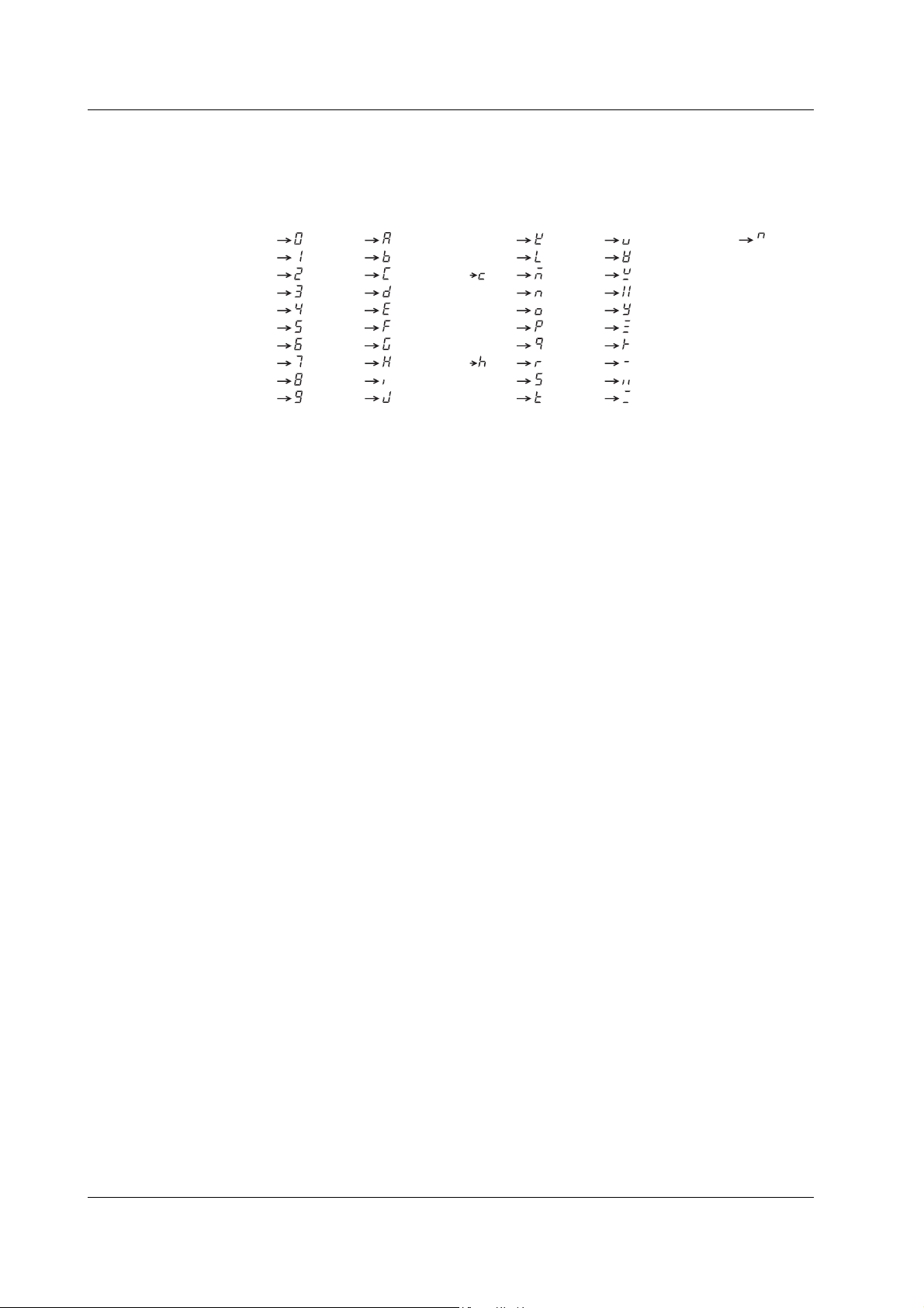
Digital Numbers and Characters
Since the instrument’s red-colored display is a 7-segment LED, it displays numbers,
alphabetical characters, and mathematical operators in a simplified form as shown
below. (Some characters are not used at all by the instrument.)
0
1
2
3
4
5
6
7
8
9
A
B
C
D
E
F
G
H
I
J
Lowercase c
Lowercase h
K
L
M
N
O
P
Q
R
S
T
U
V
W
X
Y
Z
+
–
×
÷
^(Exponent)
viii IM 704610-01E
Page 11
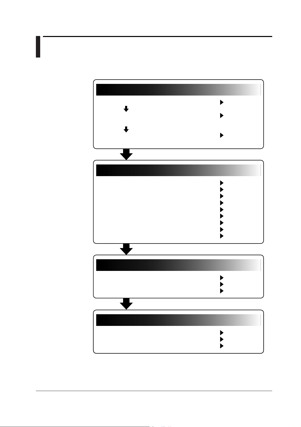
Flowchart of Operation
Preparing the Instrument
Entering Measurement Conditions
Signal Output
Displaying Measurement Results
The figure below is provided to familiarize the first-time user with the general flow of the
TA220 operation. For a more detailed description of each item, see the relevant section.
Preparing the Instrument
Installing the instrument
Connecting the power supply and
turning the power switch ON and OFF
Connecting cables and a probe
Entering Measurement Conditions
• Measurement function and polarity
• Input impedance and input coupling
• Equalizer
• Trigger mode and slice level
• Gate time
• Arming
• Block sampling
• Inhibit
• Other (as needed)
Section 3.2
Section 3.3,
Section 3.4
Section 3.5
Section 3.6
Section 4.1
Section 4.2
Section 4.3
Section 4.4
Section 4.5
Section 4.6
Section 4.7
Section 4.8
Section 4.9
Displaying Measurement Results
• Meter (needle)
• Numerical values
• Determination
Signal Output
• DC output of jitter ratio
IM 704610-01E
• DC output of RF signal voltage level
• Other signal output
Section 5.1
Section 5.2
Section 5.3
Section 7.1
Section 7.2
Section 7.3
ix
Page 12

Contents
Foreword ......................................................................................................................................... i
Checking the Contents of the Package ...........................................................................................ii
Safety Precautions .........................................................................................................................iv
Waste Electrical and Electronic Equipment....................................................................................vi
Conventions Used in This Manual................................................................................................. vii
Flowchart of Operation ...................................................................................................................ix
Chapter 1 Names and Functions of Parts
1.1 Front and Rear Panels ..................................................................................................... 1-1
1.2 Keys ................................................................................................................................. 1-2
Chapter 2 Explanation of Functions
2.1 System Configuration and Block Diagram ....................................................................... 2-1
2.2 Measurement Principle .................................................................................................... 2-3
2.3 Measurement Functions (Measurement Items) ............................................................... 2-4
2.4 Measurement Conditions ................................................................................................. 2-7
2.5 Display ........................................................................................................................... 2-13
2.6 Signal Output ................................................................................................................. 2-14
2.7 Other Functions ............................................................................................................. 2-16
Chapter 3 Preparations for Measurement and Common Operations
3.1 Handling Precautions ....................................................................................................... 3-1
3.2 Installing the Instrument ................................................................................................... 3-3
3.3 Connecting the Power Supply.......................................................................................... 3-6
3.4 Turning the Power Switch ON and OFF........................................................................... 3-7
3.5 Connecting Cables and a Probe ...................................................................................... 3-8
3.6 Correcting the Probe Phase............................................................................................. 3-9
3.7 Entering Numerical Values............................................................................................. 3-11
Chapter 4 Measurement Condition Settings
4.1 Selecting the Measurement Function and Polarity .......................................................... 4-1
4.2 Selecting the Input Impedance and Input Coupling ......................................................... 4-3
4.3 Equalizer Settings ............................................................................................................ 4-4
4.4 Setting the Trigger Mode and Slice Level ........................................................................ 4-5
4.5 Setting the Gate Time ...................................................................................................... 4-7
4.6 Setting the Arming............................................................................................................ 4-9
4.7 Block Sampling Settings ................................................................................................ 4-11
4.8 Setting Inhibit ................................................................................................................. 4-12
4.9 Other Functions ............................................................................................................. 4-14
Chapter 5 Displaying Measured Results
5.1 Meter Display ................................................................................................................... 5-1
5.2 Turning Numerical Value Display and/or Character Display ON and OFF....................... 5-3
5.3 Displaying the Jitter Ratio Determination ......................................................................... 5-5
x IM 704610-01E
Page 13

Contetns
Chapter 6 Storing and Recalling Setup Information
6.1 Storing Setup Information ................................................................................................ 6-1
6.2 Recalling Setup Information ............................................................................................. 6-2
Chapter 7 Signal Output
7.1 DC Output of Jitter Ratio .................................................................................................. 7-1
7.2 Measurement of the RF Signal Voltage Level and DC Output of the Voltage Level ........ 7-6
7.3 Outputting Other Signals................................................................................................ 7-11
Chapter 8 GP-IB Communications
8.1 About the IEEE.488.2-1992 Standard.............................................................................. 8-1
8.2 GP-IB Interface Functions and Specifications ................................................................. 8-3
8.3 Connecting the GP-IB Cable............................................................................................ 8-4
8.4 Selecting GP-IB Communications and Setting the GP-IB Address.................................. 8-5
8.5 Responses to Interface Messages................................................................................... 8-6
Chapter 9 Ethernet Communications
9.1 Ethernet Interface Functions and Specifications.............................................................. 9-1
9.2 Connecting to the Network............................................................................................... 9-2
9.3 Entering the TCP/IP and Timeout Settings, and Confirming the MAC Address ............... 9-3
Chapter 10 Communication Command
10.1 Program Format ............................................................................................................. 10-1
10.1.1 Syntactic Symbols ........................................................................................... 10-1
10.1.2 Messages ........................................................................................................ 10-1
10.1.3 Commands ...................................................................................................... 10-3
10.1.4 Response ........................................................................................................ 10-5
10.1.5 Data ................................................................................................................. 10-5
10.1.6 Synchronization with the Controller ................................................................. 10-7
10.2 Commands ..................................................................................................................... 10-9
10.2.1 Command List ................................................................................................. 10-9
10.2.2 CALCulation Group ....................................................................................... 10-12
10.2.3 COMMunicate Group .................................................................................... 10-14
10.2.4 DCOut Group ................................................................................................ 10-15
10.2.5 DISPlay Group .............................................................................................. 10-17
10.2.6 HHIStogram Group ....................................................................................... 10-19
10.2.7 INPut Group .................................................................................................. 10-20
10.2.8 LVOut Group ................................................................................................. 10-23
10.2.9 MEASure Group ............................................................................................ 10-24
10.2.10 MEMory Group .............................................................................................. 10-25
10.2.11 RECall Group ................................................................................................ 10-26
10.2.12 SAMPle Group .............................................................................................. 10-27
10.2.13 SSTart Group ................................................................................................ 10-29
10.2.14 STARt Group ................................................................................................. 10-29
10.2.15 STATus Group ............................................................................................... 10-29
10.2.16 STOP Group.................................................................................................. 10-30
10.2.17 STORe Group ............................................................................................... 10-30
10.2.18 SYSTem Group ............................................................................................. 10-31
10.2.19 UNIT Group ................................................................................................... 10-31
10.2.20 Common Command Group ........................................................................... 10-32
1
2
3
4
5
6
7
8
9
10
11
12
13
Index
IM 704610-01E
xi
Page 14

Contetns
10.3 Status Report ............................................................................................................... 10-34
10.3.1 Regarding the Status Report ......................................................................... 10-34
10.3.2 Status Byte .................................................................................................... 10-35
10.3.3 Standard Event Register ............................................................................... 10-36
10.3.4 Extended Event Register .............................................................................. 10-37
10.3.5 Output Queue and Error Queue .................................................................... 10-38
10.4 Sample Program .......................................................................................................... 10-39
10.4.1 Before Programming ..................................................................................... 10-39
10.4.2 Sample Program Interface ............................................................................ 10-39
10.4.3 Initialization/Error/Execution Function ........................................................... 10-40
10.4.4 Setting Measurement Parameters and Querying the Current Setting ........... 10-44
10.4.5 Querying the Measurement and Measured Result ....................................... 10-45
10.5 ASCII Character Codes ............................................................................................... 10-47
Chapter 11 Other Functions
11.1 Backed Up Setup Information ........................................................................................ 11-1
11.2 Initializing Settings ......................................................................................................... 11-2
11.3 Brightness Setting of the Numerical Value Display (Display 2-Green) ........................... 11-5
11.4 Turning the Key Lock ON and OFF................................................................................ 11-6
Chapter 12 Troubleshooting and Maintenance
12.1 Malfunction? First, Investigate. ..................................................................................... 12-1
12.2 Error Code Description and Corrective Actions ............................................................. 12-2
12.3 Adjusting the Zero Position of the Needle ...................................................................... 12-5
12.4 Self Diagnostics (Self Test) ............................................................................................ 12-6
12.5 Calibration (Changing the Factory Default Calibration Values)...................................... 12-9
12.6 Performance Test ......................................................................................................... 12-13
12.7 Version Display ............................................................................................................ 12-21
12.8 Replacing the Power Fuse ........................................................................................... 12-22
12.9 Recommended Replacement Parts ............................................................................. 12-23
Chapter 13 Specifications
13.1 Measurement Input, Trigger, Equalizer, and PLL........................................................... 13-1
13.2 Measurement Function .................................................................................................. 13-2
13.3 Gate Time, Arming, Block Sampling, and Inhibit............................................................ 13-2
13.4 Display ........................................................................................................................... 13-3
13.5 Input/Output on the Rear Panel ..................................................................................... 13-4
13.6 Communication Interface ............................................................................................... 13-5
13.7 General Specifications ................................................................................................... 13-6
13.8 Dimensional Drawings ................................................................................................... 13-8
Index
xii IM 704610-01E
Page 15
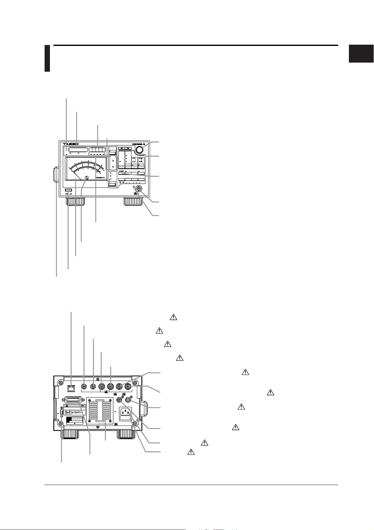
Chapter 1 Names and Functions of Parts
1.1 Front and Rear Panels
Front Panel
KEY LOCK indicator
Illuminates when key lock is ON. -> (section 11.4)
Display 2 (dot matrix green LED display)
Displays entered or selected numerical settings and other setting items.
Display 1 (7-segment red LED display)
Displays entered or selected numerical settings and other setting items.
Determination indicator
Displays jitter ratio determination results. -> (section 5.3)
DIGITAL JITTER METER
KEY
LOCK
SEC RANGE
POWER
ms s
ns
%
%/S
L.MARK
R.MARK
DISP OFF
MEASURE
V
JUDGE
NO-GO
SEC RANGE
SCALE
E2T
PW
GO
BD x1
D to C
DELAY BLOCK
GATE TIME
FUNCTION
MEDIA
ARMING INHIBIT
UTILITY
REMOTE
JDG LEVEL
POLARITY
STORE
RECALL
ENTER
LOCAL
LEVEL
EQ BOOST
COUPLE
EQUALIZER
IMPEDANCE
TRIG
50 Ω
MAN
AUTO
Ω
1M
CONV
RF
5V RMS
10%
20%
S
Unit indicator
An LED illuminates to indicate the units for the measured value or setting value being displayed.
-> (sections 5.1 and 5.2)
Adjustment trimmer
Use to adjust the zero position of the needle. -> (section 12.3)
Meter
Needle indicates measured results. -> (sections 5.1 and 12.3)
Power switch -> (section 3.4)
Handle
Use to lift or carry the instrument. -> (section 3.1)
Rotary knob
Use to enter or select numerical settings and other setting items.
Keys
Keys that are pressed first when entering a setting. Press a key to display the
corresponding selection menu. -> (section 1.2)
SHIFT key
Pressing the SHIFT key causes the SHIFT lamp above the key to illuminate,
indicating that the instrument has entered SHIFT mode. The functions marked in
purple above the panel keys are activated when the SHIFT key is pressed.
Measurement input terminal (RF input)
Terminal for connecting the RF signal measurement cable.
RF indicator
Illuminates when a trigger activates during measurement of RF signals.
->
(section 3.5)
1
Names and Functions of Parts
Rear Panel
Ethernet port -> (section 9.2)
External arming signal input terminal
Accepts input of external arming signals. -> (section 4.6)
Inhibit signal input terminal
Accepts input of inhibit signals. -> (section 4.8)
Data signal output terminal
Outputs RF signals in binary. -> (section 7.3)
Clock signal output terminal
Outputs the clock signal regenerated by the PLL circuit. -> (section 7.3)
RF signal monitor output terminal
CLOCK
OUT
EQUALIZED
MONITOR
OUT
OUT
(50 )
JITTER LEVEL
DC OUT DC OUT
(0 to +5V) (0 to +5V)
100-120V/200-240V AC
100VA MAX 50/60Hz
FUSE 250V T 5A
KEY
LOCK
ETHERNET
100BASE-TX
ACT
LINK
GP-IB(IEEE488)
WARNING
Do not operate without reading the
safety precautions in the user's manual.
MODEL
SUFFIX
NO.
Made in Japan
YOKOGAWA
EXT ARM
SLICED RF
INHIBIT
IN
OUT
IN
( 0.4V) ( 0.4V)
(TTL) (TTL) (50 )
Vent holes
-> (section 3.2)
GP-IB connector -> (section 8.3)
KEY LOCK switch
Used to turn the key lock ON and OFF. -> (section 11.4)
Outputs the RF signals input to the measurement input terminal as-is.
-> (section 7.3)
Equalized RF signal monitor output terminal
If the equalizer is activated, the equalized RF signal is output. -> (section 7.3)
Voltage level DC output terminal
Outputs the RF signals input to the measurement input terminal as DC
signals. -> (section 7.2)
Jitter ratio DC output terminal
Outputs the jitter ratio as a DC signal. -> (section 7.1)
Power connector -> (section 3.3)
Power fuse -> (section 12.8)
IM 704610-01E
1-1
Page 16
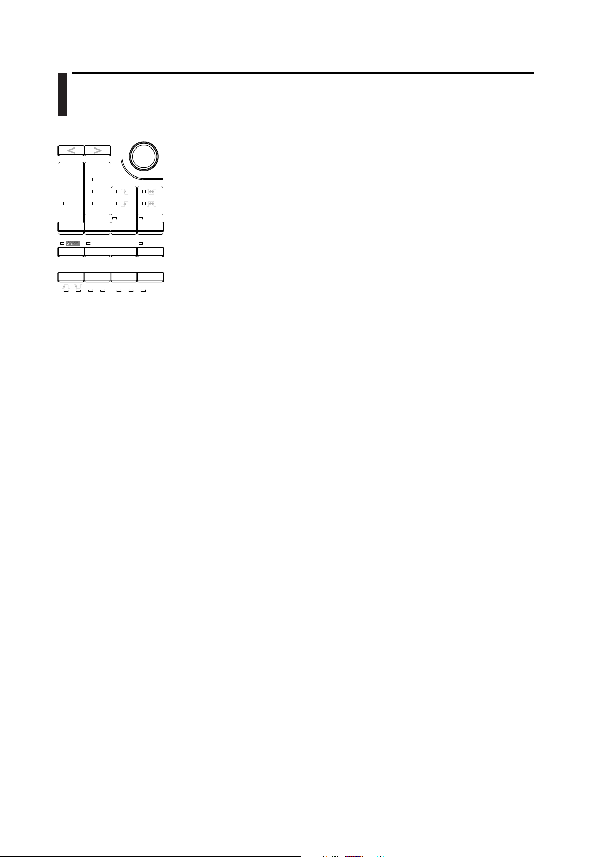
1.2 Keys
Measurement Condition Settings
L.MARK
BD x1
MEDIA
JDG LEVEL
POLARITY
R.MARK
E2T
PW
D to C
GATE TIME
FUNCTION
REMOTE
LOCAL
LEVEL
TRIG
MAN
AUTO
DELAY BLOCK
ARMING INHIBIT
STORE
RECALL
ENTER
COUPLE EQ BOOST
EQUALIZER
IMPEDANCE
50
Ω
1M
Ω
CONV
SHIFT+< (L.MARK) key and SHIFT+> (R.MARK) key -> section 4.1
When using the measurement function PW, these key combinations are used to set the
upper and lower limits of the pulse width to be measured.
MEDIA key -> sections 12.4
Press this key during self testing to execute the LED test.
FUNCTION key -> sections 4.1 and 12.4
Selects a measurement function. Also, you can press this key during self testing to
UTILITY
execute the keyboard test.
SHIFT+FUNCTION (GATE TIME) key -> section 4.5
Sets the gate time.
ARMING key -> sections 4.6 and 12.4
Selects either auto arming or external arming. Also, you can press this key during self
testing to execute the meter test.
SHIFT+ARMING (DELAY) key -> section 4.6
Sets the arming delay when external arming is selected.
INHIBIT key -> sections 4.8 and 12.4
Sets inhibit. Also, you can press this key during self testing to execute the board test.
SHIFT+INHIBIT (BLOCK) key -> section 4.7
Sets up block sampling.
POLARITY key -> section 4.1
Selects the polarity of the signal to be measured.
TRIG key -> section 4.4
Selects the trigger mode.
SHIFT+TRIG (LEVEL) key -> section 4.4
Sets the slice level.
IMPEDANCE key -> section 4.2
Selects the input impedance of the measurement input terminal.
SHIFT+IMPEDANCE (COUPLE) key -> section 4.2
Selects the input coupling of the measurement input terminal.
EQUALIZER key -> section 4.3
Equalizes the amplitude of the RF signals input to the measurement input terminal.
SHIFT+EQUALIZER (EQ BOOST) key -> section 4.3
Sets the boost amount of the equalizer.
SHIFT+ENTER (UTILITY) key -> section 4.9
Use to enter PLL hold, D-to-C high speed calculation (not available for products with
suffix code -BDS), AGC, and DC clamp settings.
1-2 IM 704610-01E
Page 17
1.2 Keys
Displaying Measurement Results
L.MARK
DISP OFF
MEASURE
JUDGE
GO
NO-GO
10%
20%
S
SEC RANGE
SCALE
BD x1
MEDIA
JDG LEVEL
POLARITY
GATE
FUNC
LOC
AUTO
R.M
E2T
PW
D t
REM
LEV
TR
CONV
MEASURE key -> sections 5.1 to 5.2
Changes the displayed measured result.
SHIFT+MEASURE (DISP OFF) key -> section 5.2
Turns OFF displays 1 and 2 (for numerical values) and the unit indicator.
SCALE key -> section 5.1
BLOCK
Selects the scale of the meter.
INHIBIT
UTILITY
SHIFT+SCALE (SEC RANGE) key -> section 5.1
ENTER
Selects the time range for the scale when the units of time for the meter scale are set to
EQ BOOST
“s”.
EQUALIZER
SHIFT+POLARITY (JDG LEVEL) key -> section 5.3
Sets the determination level when performing determination on the jitter ratio and
displaying the result as GO or NO-GO.
SHIFT+ENTER (UTILITY) key -> section 5.2
Selects the measured result displayed using the MEASURE key.
Storing/Recalling Setup Information, Signal Output, Communications, and Other
Functions
L.MARK
R.MARK
RECALL key -> section 6.2
Recalls setup info stored in the internal memory, and replaces with the current settings.
1
Names and Functions of Parts
E2T
PW
BD x1
D to C
REMOTE
LOCAL
LEVEL
TRIG
MAN
DELAY BLOCK
ARMING INHIBIT
UTILITY
STORE
RECALL
ENTER
COUPLE EQ BOOST
EQUALIZER
IMPEDANCE
Ω
50
1M
Ω
CONV
MEDIA
JDG LEVEL
POLARITY
GATE TIME
FUNCTION
AUTO
REMOTE indicator
Common Operations
L.MARK
R.MARK
E2T
PW
BD x1
D to C
REMOTE
LOCAL
LEVEL
TRIG
MAN
DELAY BLOCK
ARMING INHIBIT
UTILITY
STORE
RECALL
ENTER
COUPLE EQ BOOST
EQUALIZER
IMPEDANCE
50
Ω
Ω
1M
CONV
MEDIA
JDG LEVEL
POLARITY
GATE TIME
FUNCTION
AUTO
SHIFT+RECALL (STORE) key -> section 6.1
Stores setup information to the internal memory.
SHIFT+ENTER (UTILITY) key -> chapter 7 and sections 8.4, 9.3, 11.2, and 11.3
Use to set signal output, select the communication interface, enter a GP-IB address or
TCP/IP setting, confirm the MAC address, set the timeout time, initialize settings, set the
brightness, and display version information.
LOCAL key -> sections 8.2, 9.1, and 12.5
Returns the instrument from remote mode (when the REMOTE indicator above the
LOCAL key is illuminated) to local mode. Also, you can press this key when in
maintenance mode to execute calibration.
< > keys
Moves the selected digit when entering a value using the rotary knob and changes the
setting item.
ENTER key
When changing the selection item and entering a setting for Display 1 in the Utility menu,
pressing this key causes Display 1 to blink, indicating that the rotary knob and or < >
keys can be used to select the setting item for editing. If you press this key again while
Display 1 is blinking, it stops blinking and you can then edit the item.
IM 704610-01E
1-3
Page 18
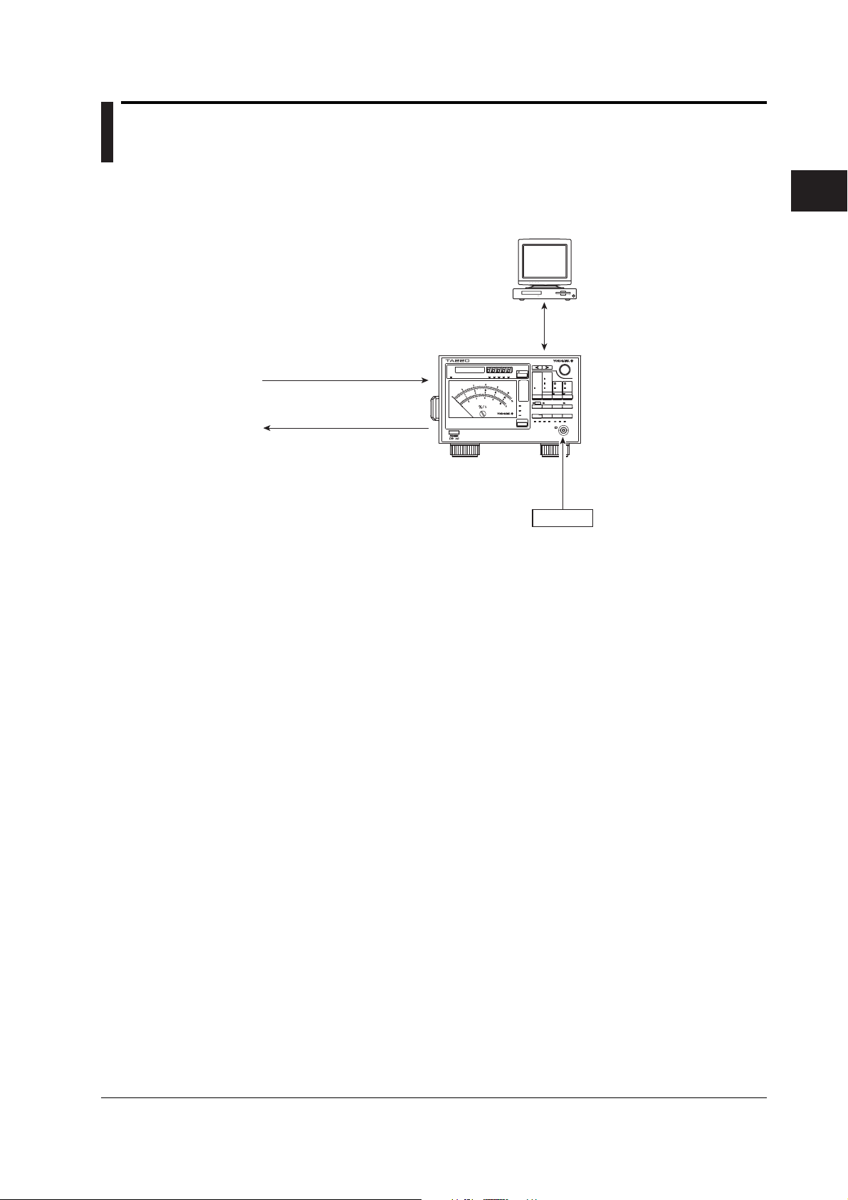
Chapter 2 Explanation of Functions
2.1 System Configuration and Block Diagram
System Configuration
Input inhibit signal
Input external arming signal
DC output of jitter ratio
DC output of the RF signal
voltage level
Monitor output of the RF signal
Monitor output of the equalized RF signal
Output of the data signal (binarized signal)
Output of the clock signal
TA220
PC
• Remote control
• Data acquisition and analysis
Communication (GP-IB/Ethernet)
Measurement input signal
RF signal
2
Explanation of Functions
IM 704610-01E
2-1
Page 19

2.1 System Configuration and Block Diagram
Block Diagram
Equalizer circuit
EQUALIZED
OUT
SLICED RF
OUT
CLOCK
OUT
EXT ARM
IN
INHIBIT
IN
JITTER
DC OUT
LEVEL
DC OUT
MONITOR
OUT
RF input
DC clamp
50 Ω
AC/DC
AGC
1 MΩ
Equalizer
Level
measurement
Slicer
Time measurement
and
measurement control
Input circuit Measurement/computation circuit
PLL
The TA220 is a jitter measuring instrument that utilizes signal processing circuits (auto slicer, equalizer,
and PLL) for support of the Blu-ray Disk standard (hereinafter, BD) of next-generation high precision
optical discs. When BD-standard RF signals are input to the instrument, the PLL circuit regenerates the
clock signal enabling measurement of the data to clock (D-to-C) jitter.
The RF signals input to the measurement input terminal (RF input) are routed through the input circuit at
the selected input coupling and input impedance, and are passed to the measurement/computation circuit
via a buffer amplifier. At the same time, signals passing through the input circuit are output from the RF
signal monitoring output terminal (MONITOR OUT) on the rear panel.
The amplitude of the signals coming from the input circuit is measured by the level measurement circuit.
The measured amplitude values are processed by the computation circuit and are sent to Display 1 (the 7segment red LED) for display. These amplitude values can also be converted to DC voltages between 0
and 5 V, and output from the voltage level DC output terminal (LEVEL DC OUT) on the rear panel.
The RF signals passing through the input circuit are routed to the equalizer circuit if the equalizer circuit is
selected. Otherwise, they are sent directly to the measurement/computation circuit.
When the equalizer circuit is selected, the RF signals pass through the DC clamp circuit (DC clamp), AGC
amplifier (AGC), and variable boost equalizer circuits (equalizer), and are converted to binary values by the
autoslice (slicer) circuit. Binarized data signals are input to the PLL circuit (PLL), and the clock signal is
regenerated. Data and clock signals are input to the measurement/computation circuit where the D-to-C
time (phase difference) is measured and jitter values are calculated. RF signals prior to binarization that
are processed in the equalizer are output from the equalized RF signal monitoring output terminal
(EQUALIZED OUT) on the rear panel, or, data signals and clock signals are output from the data signal
output terminal (SLICED RF OUT) and clock signal output terminal (CLOCK OUT) on the rear panel,
respectively.
The DC clamp circuit function is used to stabilize input RF signals with DC components such as can occur
with mirror portions of discs. This circuit temporarily adjusts the low-band cutoff frequency from 10 kHz to
3 MHz, thereby quickly attenuating the fluctuating DC component. The DC clamp circuit is active during
the inhibit period.
The variable boost equalizer circuit has the equalizing characteristics shown by the transfer function below,
and the characteristics of a 3rd order Bessel LPF (lowpass filter, 3 dB attenuation point 30 MHz)
connected in cascade. You can set the difference in gain at 100 kHz and 16.5 MHz as the boost amount.
H(z)=1/2{–k+(1+k)z–1+(1+k)z–2–kz–3}
The autoslice circuit consists of a first order integration feedback circuit. It uses a function that superimposes
DC voltage on the slice level, and you can change the slice level when the RF signal is binarized.
In the measurement/computation circuit, signal acquisition is controlled according to external arming and
inhibit signals (EXT ARM and INHIBIT), time measurement and computation is performed on the acquired
data, and jitter, jitter ratio, and average values are calculated. The results are shown by the meter needle
and the value displayed on Display 1. In addition, the jitter ratio can also be converted to a DC voltage
between 0 and 5 V, and output from the jitter ratio DC output terminal (JITTER DC OUT) on the rear panel.
2-2 IM 704610-01E
Page 20
2.2 Measurement Principle
Measured signal
Measurement clock
Fractional pulse
Time-voltage conversion
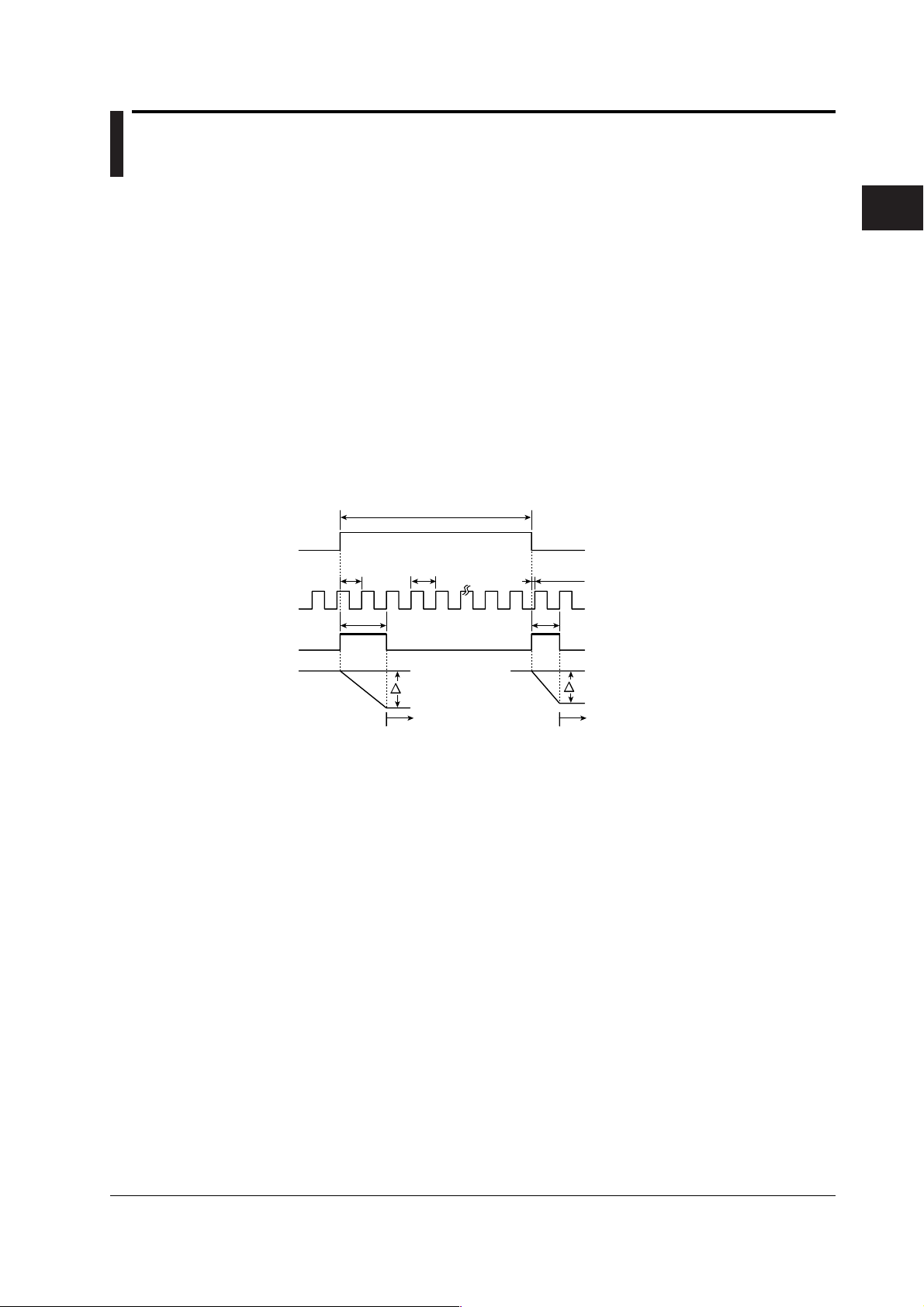
Example with Pulse Width Measurement
A time shorter than the period of the measurement clock is called the fractional time. In
general, since the measured signal and the measurement clock are not synchronized,
fractional time exists both at the beginning and at the end of measurements. This
instrument generates a “fractional pulse” which is a pulse signal equal to the sum of the
fractional time and one period of the measurement clock. Given pulse width T of the
measured signal, measurement clock period t
, and fractional pulse times Ta and Tb,
0
pulse width T can be divided into integer multiples of the measurement clock time N
times t
and fractional pulse times Ta and Tb as follows:
0
T = N • t0 + (Ta – Tb)
The instrument converts the fractional pulse times on the starting and ending sides (T
a
and Tb) to voltage values. By then converting those voltages to digital values using 7-bit
A/D conversion, the fractional pulse widths can be measured at time resolutions of
approximately 100 ps per 1LSB. T is determined by substituting the measured fractional
pulse times with T
Fractional time
T
and Tb in the equation above.
a
T
t
12
a
0
V = k · T
a
a
Fractional time
N
T
b
T = N · t0 + (Ta – Tb)
k: Coefficient used in the A/D conversion
V = k · T
b
b
2
Explanation of Functions
A/D conversion
A/D conversion
IM 704610-01E
2-3
Page 21
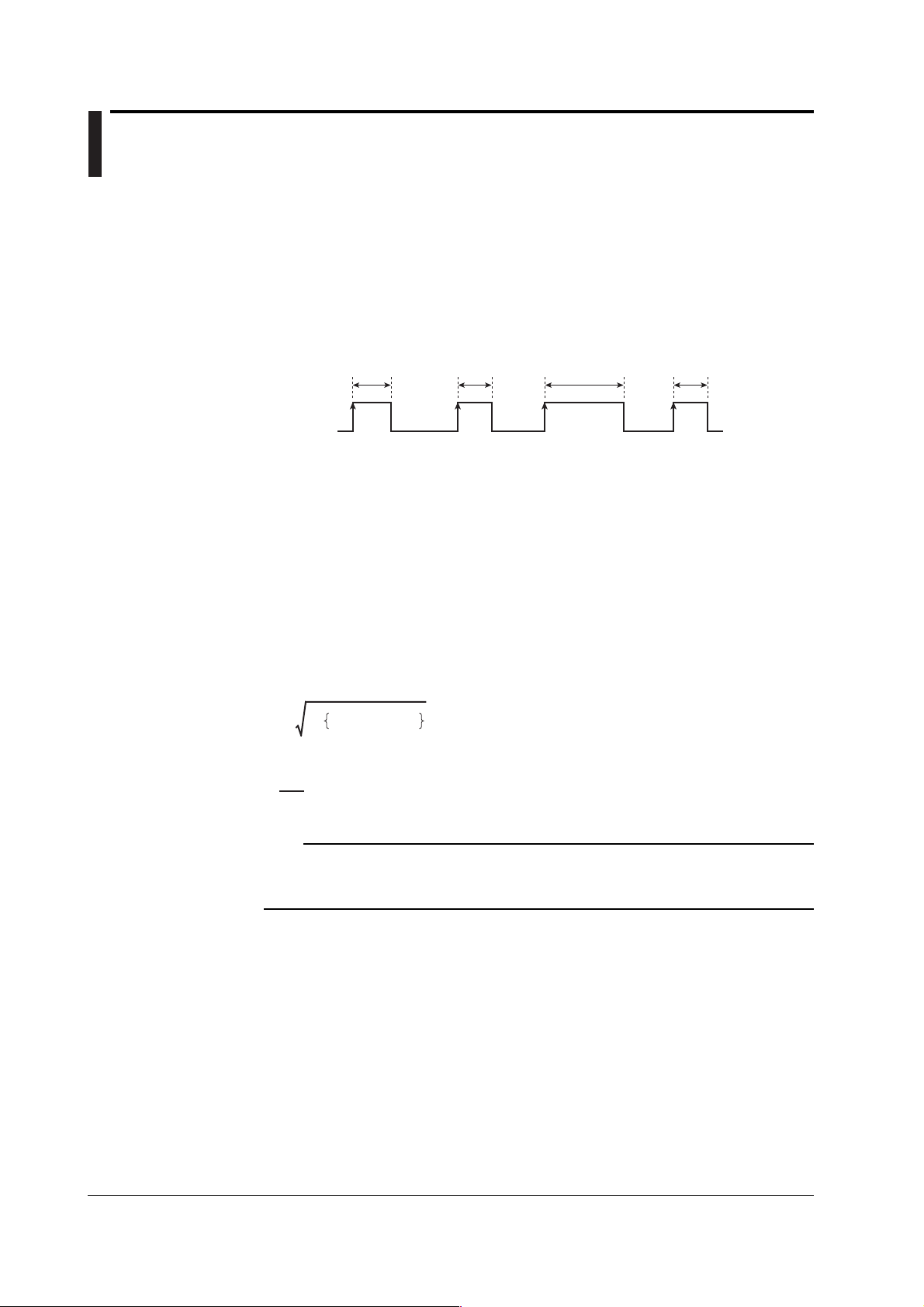
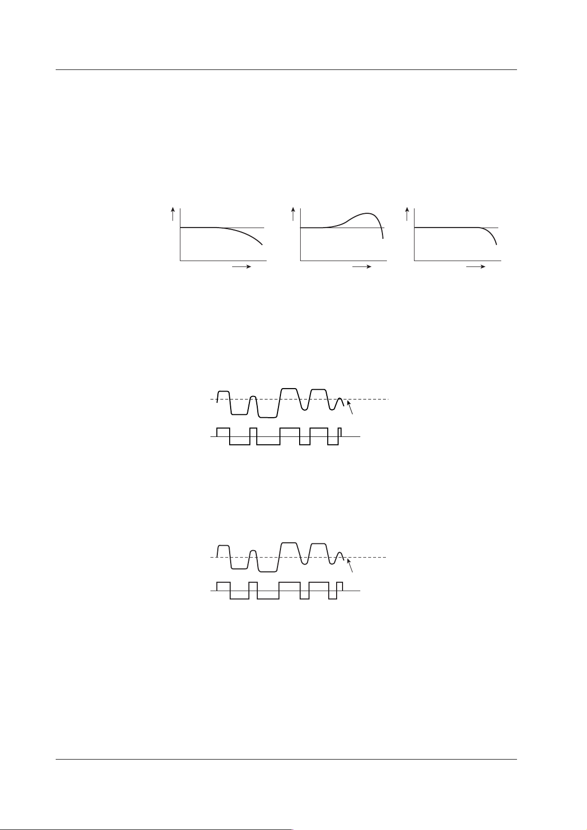
2.3 Measurement Functions (Measurement Items)
Pulse Width Jitter <<For procedures, see section 4.1>>
Pulse Width Measurement
You can measures the pulse width from the rising edge of the slope* to the next falling
edge of the slope (positive side) or from the falling edge of the slope to the next rising
edge of the slope (negative side) of the data signal.
* The slope of a signal is its movement from a low level to a high level (rising), or from a high
level to a low level (falling).
Example of positive side pulses
Measurement Measurement Measurement Measurement
Data
signal
Jitter σ, Jitter Ratio σ/T, and Average Value
A histogram (frequency distribution) is created from multiple pulse widths within a
specified range (see “Upper and Lower Limits of the Pulse Width” on page 2-6), and the
standard deviation σ of the values making up the histogram is calculated. This standard
deviation σ is the pulse width jitter. The percentage calculated when dividing the
standard deviation σ by the difference T in the upper and lower limits of the pulse width
is called the pulse width jitter ratio. The time-averaged value of the measured pulse
width signal is the pulse width average value (AVE).
• Pulse width jitter
• Pulse width jitter ratio
• Pulse width average value
n
AVE =
σ = Σ (Xi – AVE)2 × P
σ
T
Xi × P
Σ (
i = 1
n
i = 1
× 100(%)
i
)
n: Number of bins (histogram lines) of the histogram
X
i
: Class value of each bin
i
P
i
: Relative frequency
(Ratio of frequency X
total number of samples)
T: Difference between the upper and lower limit of
the pulse width.
i
of a single bin with respect to the
Note
By switching the displayed numerical value (see section 5.2) and making queries through
communication commands (see section 10.2.2) you can obtain statistical values other than
the jitter, jitter ratio, and average value.
2-4 IM 704610-01E
Page 22

2.3 Measurement Functions (Measurement Items)
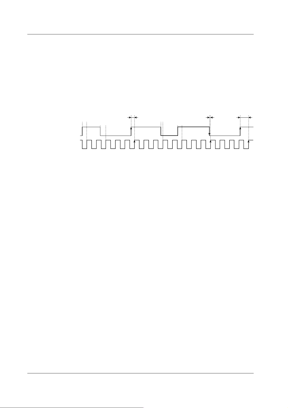
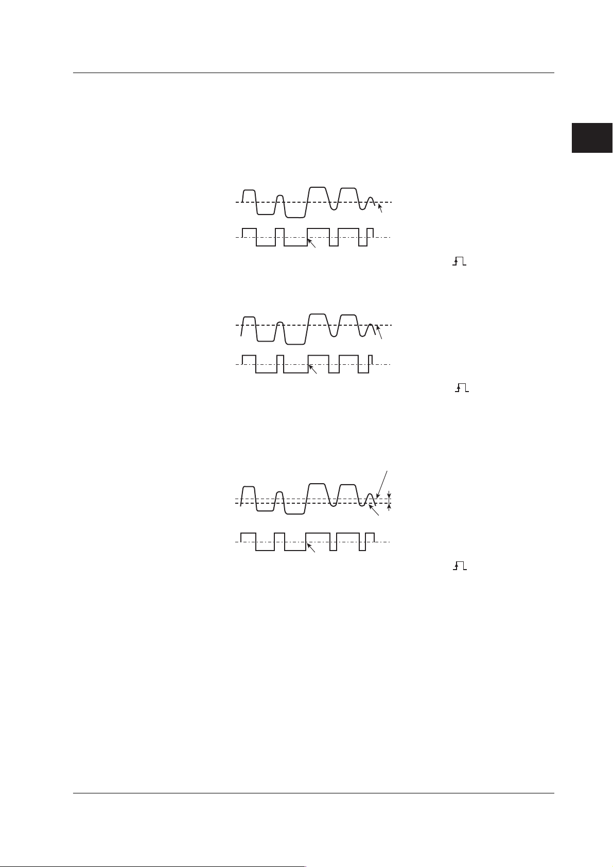
D-to-C Jitter <<For procedures, see section 4.1>>
Measuring Phase Difference
You can measure the phase (time) difference from the rising (or falling) slope of the data
signal to the first rising slope of the clock signal.
• Example 1
Data signal slope: rising
Clock signal slope: rising
Measurement Measurement
Data
signal
Clock
signal
• Example 2
Data signal slope: both rising and falling
Clock signal slope: rising
Measurement
Measurement
Data
signal
Clock
signal
Measurement
2
Explanation of Functions
Jitter σ, Jitter Ratio σ/T, and Average Value
A histogram (frequency distribution) is determined from multiple measured values of
phase difference, and the standard deviation σ from the histogram is calculated. This
standard deviation σ is the D-to-C jitter. The D-to-C jitter ratio is derived as a percentage
by dividing the standard deviation σ by the period T of the clock signal. The timeaveraged value of the measured phase difference signal is the D-to-C average value
AVE.
• D-to-C average value
• D-to-C jitter
• D-to-C jitter ratio
n
AVE =
σ = Σ (Xi – AVE)2 × Pi
σ
T
Xi × Pi
Σ (
i = 1
n
i = 1
× 100(%)
)
n: Number of bins (histogram lines) of the histogram
Xi: Class value of each bin
Pi: Relative frequency
(Ratio of frequency Xi of a single bin with respect
to the total number of samples)
T: Period of the clock signal
(differs depending on the signal being measured since
it is measured at the same time as the data signal)
Regenerating the Clock Signal
The clock signal that is necessary in measuring the D-to-C jitter can be regenerated by
the PLL circuit of the instrument. D-to-C jitter measurements are carried out using the
regenerated clock signal. You can display the period T of the regenerated clock signal.
IM 704610-01E
Note
By switching the displayed numerical values (see section 5.2) and making queries through
communication commands (see section 10.2.2), you can obtain statistical values other than
the jitter, jitter ratio, and average value.
2-5
Page 23
2.3 Measurement Functions (Measurement Items)
D-to-C Jitter Excluding 2T <For the setup procedure, see section 4.1>
This is one of the functions available for measuring D-to-C jitter. D-to-C jitter is
measured, excluding the phase difference of data signals having pulse widths of two
times the clock signal period (2T) or less. When the pulse width of the data signal is 2T
or less, the phase difference before and after that data signal is not measured.
The method for determining the jitter σ, jitter ratio σ/T, and average value is the same as
that for normal D-to-C jitter.
D-to-C jitter excluding 2T cannot be measured by products with suffix code -BDS.
Example
Slope of the data signal: Both rising and falling
Slope of the clock signal: Rising
Measured
Data
signal
Clock
signal
Not measured
Not measured
2T 3T 3T 3T 3T 4T2T
Not measured
Not measured
Measured Measured
2-6 IM 704610-01E
Page 24
2.4 Measurement Conditions
Measurement Block
The TA220 repeats a three-part process of measurement, data processing, and display.
The smallest unit that is measured during the first part of this process is called a
measurement block. In the figure below, N is the number of samples (number of data)
acquired in a single pass of the process, and the measurement, data processing, and
display of these samples is considered to be one block of measurement. The range of
measured blocks is specified by the gate time described below.
Pulse Width Measurement
1 block
Measurement block
S1 S1 S2 S3S2 S3 SN
Measurement input signal
Preparing for measurement
Data processing
-display
1 block
Measurement block
Upper and Lower Limits of the Pulse Width <<For procedures, see section 4.1>>
Optical disc signals are pulse signals having time widths that are integer multiples of a
reference item width T (for example, 2T–14T, etc.). The pulses can experience
variations (jitter), such that for example a 3T pulse signal may include time widths of 2.9T
or 3.1T. You can specify to measure only pulse signals within a certain range of these
variations (for example a range from 2.5T to 3.5T).
Input Impedance <<For procedures, see section 4.2>>
To attenuate the measured signal and reduce distortions, you must adjust to the output
impedance of the signal under test. You can select an input impedance for the
measurement input terminal of 50 Ω or 1 MΩ.
2
Explanation of Functions
Input Coupling <<For procedures, see section 4.2>>
Measurement of only the amplitude (AC component) of the measurement input signal or
only signals superimposed with a specific DC voltage is simplified by removing the DC
component of the signal. There are also times when you wish to measure the input
signal without removing the DC component. In these cases, you can change the input
coupling setting and apply the signal to the input amp. The following types of input
coupling are available.
AC
Input is passed through a capacitor, removing the DC component. This coupling should
be used when measuring only the amplitude of the signal, or when measuring only
signals superimposed with a specific DC voltage.
Measurement input terminal
DC
Inputs the signal directly. Use this setting if you wish to measure the entire input signal
(DC component and AC component).
Measurement input terminal
Note
When the equalizer is ON, the signal is AC-coupled through the cutoff frequency of 10 kHz
inside the equalizer regardless of the above coupling setting.
Input
amp
Input
amp
IM 704610-01E
2-7
Page 25
2.4 Measurement Conditions
Equalizing RF Signals (Equalizer) <<For procedures, see section 4.3>>
You can equalize the signal amplitude in the high frequency region. The signal
amplitude in the high frequency region attenuates due to the frequency characteristics of
the optical pickup. By passing the RF signal that is applied to the measurement input
terminal through the equalizer, you can obtain a signal that has frequency characteristics
that do not attenuate up to the high frequency region (better frequency characteristics
than the optical pickup).
Frequency characteristics of
the signal applied to the
measurement input terminal
Amplitude
Frequency
Binarization of the RF Signal
The signal used to measure the pulse width and phase difference is a data signal
binarized from the RF signal applied to the measurement input terminal. Using the slicer
of the TA220, the RF signal is binarized by setting the portion of the signal that is greater
than the given slice level* to the positive side and the portion that is less than the slice
level to the negative side.
* The slice level changes depending on the trigger mode setting. For information on setting the
trigger mode and slice level, see “Trigger Mode and Slice Level” below.
RF signal
Data signal
Auto Slice
To correct the asymmetrical signal waveforms typical of optical disks, a slice level is
automatically detected such that the time ratio of the positive and negative sides of the
RF signal is 50%. The RF signal is binarized using the detected slice level. The auto
slice function operates when the trigger mode is set to “auto mode” or “auto + manual
mode” as described below.
Frequency characteristics
of the equalizer
Amplitude
Frequency
Positive side
Negative side
Slice level
Frequency characteristics
of the signal after passing
through the equalizer
Amplitude
Frequency
RF signal
Data signal
Positive side
Negative side
Slice level
2-8 IM 704610-01E
Page 26
2.4 Measurement Conditions
Trigger Mode and Slice Level <<For procedures, see section 4.4>>
When measuring the pulse width or phase difference of a single pulse, you can select
the level of the data signal at which to make the measurement (activate the trigger). Slice
level refers to the signal level used to binarize the RF signal.
Auto mode
The RF signal is binarized using the slice level that is detected by the auto slice function.
RF signal
Slice level that is detected
by the auto slice function
Data signal
Trigger is activated
(when the polarity or slope is set to )
Manual mode
The RF signal is binarized using a specified slice level.
RF signal
Center value of the amplitude
The specified slice level
2
Explanation of Functions
Data signal
Trigger is activated
(when the polarity or slope is set to )
Center value of the amplitude
Auto + manual mode
The RF signal is binarized using the slice level detected with the auto slice function
superimposed by a specified offset slice level. The offset level that is superimposed is
set separately from the slice level of the manual mode described above.
Slice level that is detected
by the auto slice function
RF signal
Data signal
Trigger is activated
(when the polarity or slope is set to )
(Offset) level that is superimposed
Slice level for auto + manual mode
Center value of the amplitude
IM 704610-01E
2-9
Page 27

2.4 Measurement Conditions
Gate Time <<For procedures, see section 4.5>>
You can set the time (gate time) during which the measured values of pulse width and
phase difference are stored in the acquisition memory.
Arming <<For procedures, see section 4.6>>
Arming refers to the cue used to start the measurement. As opposed to a trigger, which
refers to the cue used to measure the pulse width or phase difference of each pulse,
arming refers to the starting point of the measurement of a set of pulse widths or phase
differences used to derive the jitter.
Auto Arming (Internal Arming)
The internal signal of the TA220 is the arming source. Arming is the cue used to start the
first measurement (the first trigger).
External Arming
Arming is activated when an external signal (arming source) is applied to the external
arming input terminal. You can also select whether the rising or falling edge is used to
activate the arming.
Arming Delay
When using external arming, you can delay the start of the measurement by a given
amount of time (delay time) after arming occurs.
Block Sampling <<For procedures, see section 4.7>>
Repeating one block of measurement a specified number of times is called block
sampling. With block sampling, all data collected after performing one block of
measurement a specified number of repetitions is processed and displayed together.
Block sampling measurement is available when external arming is active.
Arming delay
External arming
signal
Input signal
First block
S1 S2 S3 S1 S2 S3
Start measurement
Arming delay
Second block
Start measurement
2-10 IM 704610-01E
Page 28
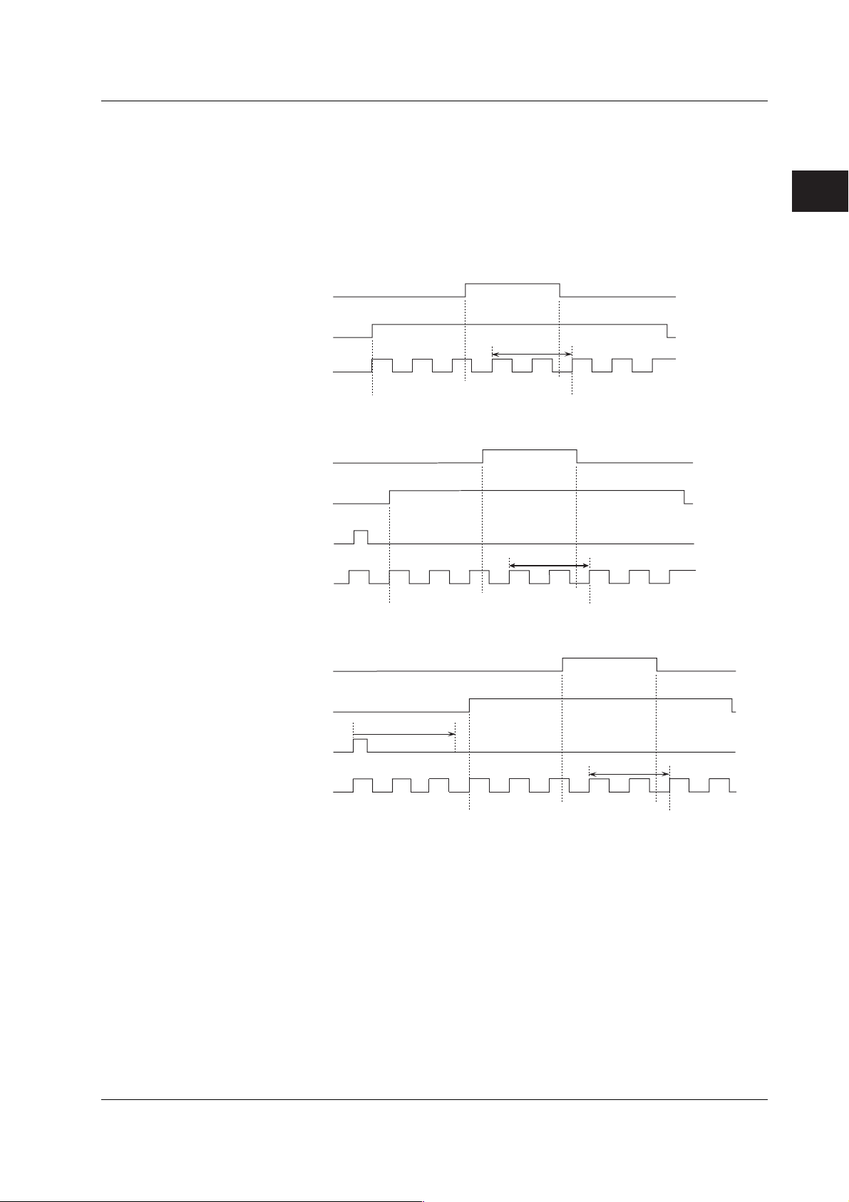
Inhibit <<For procedures, see section 4.8>>
You can inhibit measurements by applying an external signal to the inhibit signal input
terminal. This is possible even while the gate is open or during measurement after
arming activation. You can also select which polarity of the signal, positive or negative, is
used to inhibit measurements. The relation between the inhibit signal, gating, and
arming for pulse width jitter measurement is indicated below.
Relation between the Inhibit Signal and Gating
Inhibit
2.4 Measurement Conditions
2
Explanation of Functions
Inhibits measurement
Gate
Data signal
Gate open
Not measured
S1 S2 S3 S4 S5
Starts measurement
Resumes measurement
Relation between the Inhibit Signal, Gating, and External Arming
Inhibits measurement
Inhibit
Gate
External arming
Data signal
Gate open
Not measured
S1 S2 S3 S4 S5
Starts measurement
Resumes measurement
Relation between the Inhibit Signal, Gating, External Arming, and Arming Delay
Inhibits measurement
Inhibit
Gate open
Gate
Arming delay
External arming
Not measured
Data signal
S1 S2 S3 S4 S5
Starts
measurement
Resumes
measurement
IM 704610-01E
2-11
Page 29
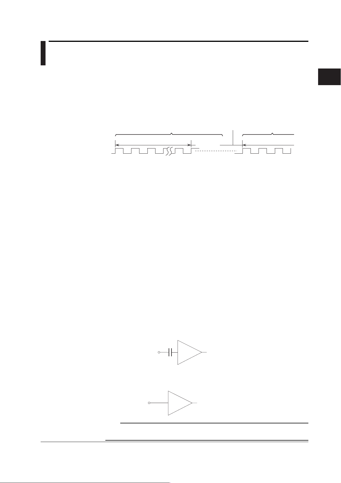
2.4 Measurement Conditions
PLL Hold <<For procedures, see section 4.9>>
The PLL hold function maintains the frequency of the clock signal regenerated in the PLL
circuit when Inhibit is active. If RF signals whose clock signals cannot be regenerated in
the PLL circuit are input to the measurement input terminal when Inhibit is active, once
Inhibit is cleared, if a normal RF signal whose clock signal can be regenerated in the PLL
circuit is then introduced, the clock signal will be generated normally.
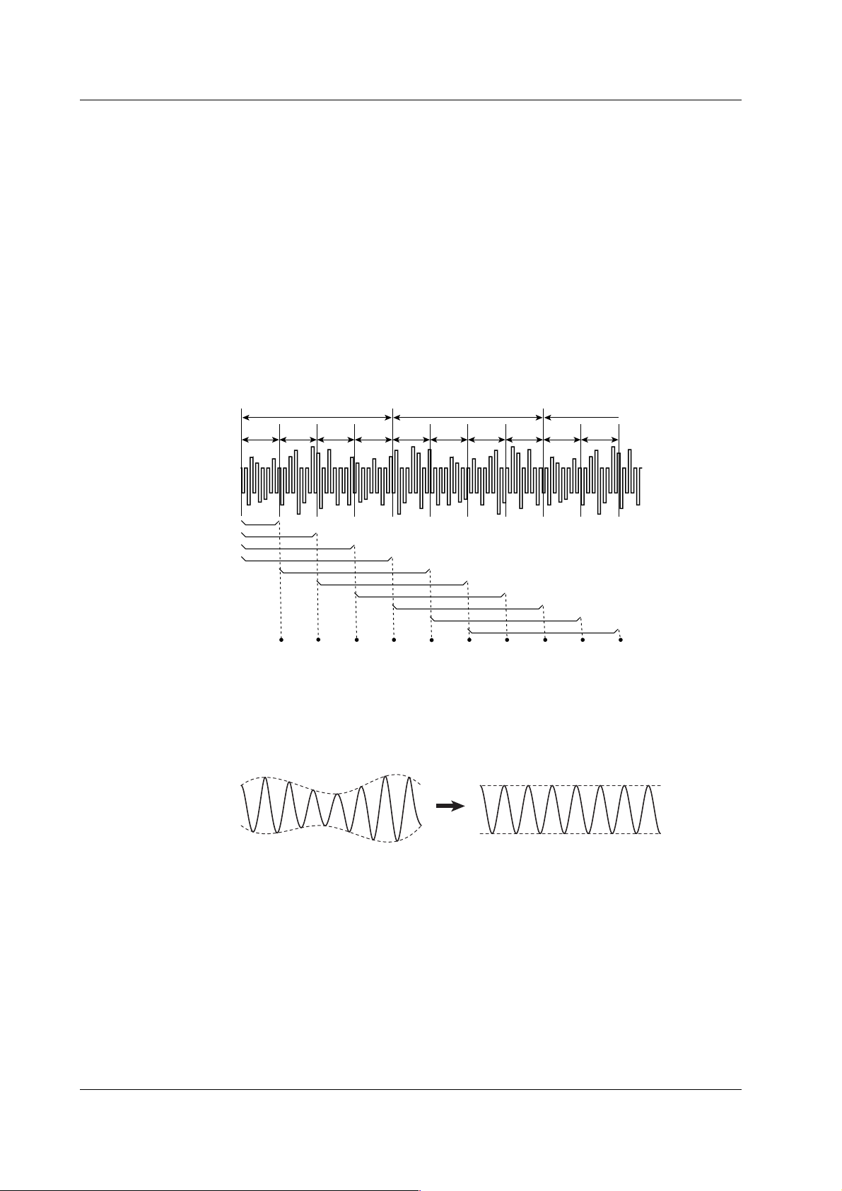
D-to-C High Speed Calculation <For the setup procedure, see section 4.9>
With normal D-to-C jitter measurement, when this function is enabled the measured Dto-C jitter is updated every 2 ms rather than being updated according to a specified gate
time. For example, if the gate time is set to 8 ms, the measured values of the
measurement clock delimited every 2 ms as in the figure below is moving-summed over
an 8-ms time range, and the results are updated every 2 ms.
The D-to-C high speed calculation function is not available on products with suffix code BDS.
Gate time of 8 ms Gate time of 8 ms Gate time of 8 ms
2 ms 2 ms 2 ms 2 ms 2 ms 2 ms 2 ms 2 ms 2 ms 2 ms
Outputs the moving-summed result every 2 ms.
The summing time is the same as the gate time.
AGC (Automatic Gain Control Amplifier) <<For procedures, see section 4.9>>
If undulations occur in the signal amplitude envelope, the signal can be applied to an
AGC circuit to normalize the fluctuations in the amplitude thereby improving the accuracy
of jitter measurements.
DC Clamp <<For procedures, see section 4.9>>
If RF signals with temporarily changing DC components are applied to the measurement
input terminal when Inhibit is active, the DC clamp function can be used to quickly
attenuate the changed portion of the DC components. The low-band cutoff frequency in
the equalizer circuit is changed from 10 kHz to 3 MHz, the changed portion of the DC
component is immediately attenuated, and regeneration of the clock signal by the PLL
circuit is maintained.
2-12 IM 704610-01E
Page 30

2.5 Display
Meter Display <<For procedures, see section 5.1>>
The TA220 indicates the jitter and jitter ratio on the analog meter.
Jitter Ratio Indication
The jitter ratio of the selected measurement function is indicated on the analog meter.
You can select a scale for the meter of 10% or 20%. The indication range is 0% to 11%
for the 10% scale and 0% to 22% for the 20% scale.
Jitter Indication
The jitter of the selected measurement function is indicated on the analog meter. The
scale is marked in units of time (seconds) on the bottom of the meter. You can switch
the range of the scale from 0.5 ns to 5.0 µs. The range is shown on Display 2.
Display of Numerical Values and Characters
The TA220 displays numerical values and alphabetical characters such as the jitter, jitter
ratio, average value, specified value, error code, and firmware version on Display 1 or
Display 2.
Numerical Display of Measured Results <<For procedures, see section 5.2>>
Measured results (the jitter ratio, jitter, and average value) are displayed numerically on
Display 1. Display 1 is a red 7-segment LED. Display 1 is used for settings, error codes,
and the firmware version.
2
Explanation of Functions
Character and Numerical Display of Setting Parameters and Values
Setting parameters are shown using alphabetical characters on Display 2. Display 2 is a
green dot matrix LED. For certain setting parameters, you can display the numerical
measured result on Display 1 while simultaneously displaying a setting parameter and
setting value on Display 2.
Turning OFF Numerical/Character Display <<For procedures, see section 5.2>>
If you are distracted by the changing jitter ratio, jitter, or average values, or blinking
setting values, you can turn both Display 1 and Display 2 OFF.
Determination Display of Jitter Ratio <<For procedures, see section 5.3>>
You can set the determination level for the jitter ratio and display determination results as
GO or NO-GO. The GO indicator illuminates in green when the jitter ratio is less than or
equal to the determination level, and the NO-GO indicator illuminates in red when the
jitter ratio exceeds the determination level. If a clock signal can not be regenerated by
the PLL circuit during D-to-C measurement, both GO and NO-GO indicators illuminate in
green and red respectively.
IM 704610-01E
2-13
Page 31

2.6 Signal Output
DC Output of the Jitter Ratio <<For procedures, see section 7.1>>
DC Output of the Jitter Ratio
The jitter ratio of the selected measurement function can be linearly converted to DC
voltage (0 to 5 V) and output from the jitter ratio DC output terminal on the rear panel.
You can also change the jitter ratio that corresponds to 0 V and 5 V.
Jitter Ratio Determination Output
You can specify the determination level in terms of a jitter ratio and output 5 VDC from
the jitter ratio DC output terminal when the data signal is less than or equal to the
determination level, and 0 VDC when it is greater than the determination level.
DC Output Filter
This filter takes the moving average of the measured jitter ratio. When the DC output
fluctuates due to instability in the measured jitter, this function suppresses the degree of
fluctuation. You can set the number of measured values (average coefficient) to be
averaged in the range from 1 to 10. The moving-averaged jitter ratio is shown on the
numerical display and analog meter, and sent to DC output.
When the average coefficient is set to 5
Measured
jitter ratio
Jitter ratio
after moving
average
D
B
C
A
G
F
E
Time
c
b
a
Time
Jitter Ratio Correction Coefficients
The specified jitter ratio can undergo 1st order correction per the specified correction
coefficients. Two correction coefficients can be specified, α (slope) and β (offset value).
The jitter is the value obtained by multiplying the corrected jitter ratio by time T (see
section 2.3). The corrected jitter and jitter ratio are shown on the numerical display and
analog meter, and sent to DC output.
Jitter Ratio Correction Equation
J
= αJm + β
c
Jc: corrected jitter ratio, Jm: uncorrected jitter ratio
2-14 IM 704610-01E
Page 32

2.6 Signal Output
Measurement of the RF Signal Voltage Level and DC Output of the Voltage Level
<<For procedures, see 7.2 section >>
Voltage Level Measurement
RF signals input to the amplitude measurement circuit pass through a filter than removes
noise and overshoot. Next, the A/D converter in the amplitude measurement circuit
measures the maximum and minimum values of the input signal, and the difference
between the two is taken as the RF signal’s voltage level.
Maximum value
Minimum value
2
Explanation of Functions
Input signal
Voltage Level Display
When RF signal voltage measurement is ON, you can switch the display to view the
measured numerical voltage level values on the same display.
DC Output of Voltage Levels
The voltage level of the RF signal can be linearly converted to DC voltage (0 to 5 V) and
output from the voltage level DC output terminal on the rear panel. You can also change
the RF signal voltage level that corresponds to the 0 and 5 V levels.
Voltage Level Determination Output
The upper and lower limits of the determination range can be set according to the RF
signal voltage levels so that 5 VDC is output when the signal falls between the upper and
lower limits, and 0 VDC is output when the upper limit is exceeded or the lower limit is
not reached.
DC Output Filter for Voltage Levels
A moving average can be taken of the RF signal voltage levels. When the DC output
fluctuates due to instability in the RF signal voltage levels, this function suppresses the
degree of fluctuation. You can set the number of measured values (average coefficient)
to be averaged in the range from 1 to 10. The operation is the same as that of the jitter
ratio DC output filter on the previous page.
Filtered waveform
Monitor Output of RF Signals <<For procedures, see section 7.3>>
You can output the RF signals applied to the measurement input terminal as-is from the
RF signal monitor output terminal on the rear panel.
Monitor Output of Equalized RF Signals <<For procedures, see section 7.3>>
If the equalizer is activated, the equalized RF signal is output. When AGC is ON, the RF
signal passes through the AGC circuit before being output. When AGC is OFF and the
equalizer is not activated, the signal bypasses the AGC and equalizer circuits.
Data Signal Output <<For procedures, see section 7.3>>
You can output the data signal obtained by slicing and binarizing the RF signal from the
data signal output terminal on the rear panel.
Clock Signal Output <<For procedures, see section 7.3>>
You can output the clock signal regenerated by the PLL circuit from the clock signal
output terminal on the rear panel.
IM 704610-01E
2-15
Page 33

2.7 Other Functions
Storing and Recalling Setup Information <<For procedures, see chapter 6>>
Up to seven sets of setup information can be stored in the internal non-volatile memory.
You can also recall the stored setup information and change the settings.
Communication Using Commands (GP-IB or Ethernet) <<For procedures, see
chapters 8 and 9, and the explanation of commands in chapter 10>>
The TA220 comes standard with GP-IB and Ethernet interfaces. You can output the
jitter or jitter ratio of the selected measurement function to a PC or control the TA220
from an external controller.
Backing Up of Setup Information <<For procedures, see section 11.1>>
The setup information is stored using a lithium battery. When the power switch is turned
ON, the TA220 starts measurement using the settings that existed immediately before
the power switch was turned OFF. If the setup information can no longer be stored due
to a dead lithium battery, the TA220 is reset to the factory default settings.
Initializing Setup Information <<For procedures, see section 11.2>>
The following two methods are available for initializing setup information on the instrument.
• Initialization to factory default settings
• Initialization of all setup information except the following.
Network related set up information
Setup information stored to the internal memory
Digital display (green) brightness setting
Digital Display (Green) Brightness Setting <<For procedures, see section 11.3>>
You can change the brightness of Display 2.
Key Lock <<For procedures, see section 11.4>>
You can disable the front panel key operation.
Adjusting the Zero Position of the Needle <<For procedures, see section 12.3>>
You can adjust the zero position of the needle.
Self Test <<For procedures, see section 12.4>>
If you are in doubt as to whether the instrument has malfunctioned, you can run a self
test before contacting a YOKOGAWA dealer. You can check things such as the keys,
rotary knob, indicator, meter, and boards.
Calibration <<For procedures, see section 12.5>>
Using the internal calibration signal, the offset voltage of the input amplifier and the
conversion coefficient of the time-voltage converter can be calibrated.
Version Display <<For procedures, see section 12.7>>
The firmware version (ROM version) of the TA220 can be displayed.
Detection of a Cooling Fan Malfunction
The condition of the cooling fan is monitored at all times. If the fan stops, error code 906
is shown on the display. If this occurs, immediately turn OFF the power. If you continue
to use the instrument, a warning is given approximately every ten seconds by displaying
the error code until the cooling fan recovers.
2-16 IM 704610-01E
Page 34

Chapter 3 Preparations for Measurement and Common Operations
3.1 Handling Precautions
Safety Precautions
Symbols Used on This Instrument
When using the instrument for the first time, make sure to read the “Safety Precautions”
given on pages iv and v.
Do Not Remove the Cover from the Instrument
Do not remove the instrument case. Some parts of the instrument use high voltages,
which are extremely dangerous. For internal inspection or adjustment, contact your
nearest YOKOGAWA dealer.
Cut the Power in Case of Irregularity
If there are any symptoms of trouble such as strange smells or smoke coming from the
instrument, turn the power OFF immediately, and remove the power cord from the outlet.
If such an irregularity occurs, contact your YOKOGAWA dealer.
Turn OFF the Instrument If the Cooling Fan Stops
If error code 906 appears on the display, the cooling fan is stopped. Immediately turn
OFF the power switch. From the rear panel, check for and remove any foreign object that
may be obstructing the cooling fan. If error message 906 appears when you turn ON the
power switch again, it is probably a malfunction. Contact your YOKOGAWA dealer.
Handle the Power Cord Correctly
Nothing should be placed on top of the power cord. The power cord should also be kept
away from any heat sources. When unplugging the power cord from the outlet, never pull
by the cord itself. Always hold and pull by the plug. If the power cord is damaged, check
the part number indicated on page ii and purchase a replacement.
3
Preparations for Measurement and Common Operations
IM 704610-01E
3-1
Page 35

3.1 Handling Precautions
General Handling Precautions
Do Not Place Objects on Top of the Instrument
Never place any objects containing water on top of the instrument. Doing so can lead to
malfunction.
Do Not Apply Physical Shock or Vibration to the Instrument
Do not apply physical shock or vibration to the instrument. Doing so can lead to
malfunction. Take extra caution because the built-in meter is sensitive to vibration and
shock. In addition, applying shock to the input terminal or the connected cable can cause
electrical noise to enter the instrument.
Keep Electrically Charged Objects Away from the Instrument
Do not bring charged objects near the input connector. Doing so could cause damage to
the instrument’s internal circuitry.
Unplug During Periods of Extended Non-Use
When not using the instrument for a long period of time, turn OFF the power switch and
remove the power cord from the outlet.
Moving the Instrument
Remove the power cord and all connected cables before moving the instrument. The
instrument weighs approximately 5 kg. Always carry the instrument carefully by the
handle (as shown below) when moving it.
Clean the Instrument Properly
When wiping off dirt from the case or operation panel, turn OFF the power switch and
remove the power cord from the outlet. Then, gently wipe with a soft dry clean cloth. Do
not use chemicals such as benzene or thinner, since these may cause discoloring and
deformation. Do not bring charged objects near the signal terminals.
3-2 IM 704610-01E
Page 36

3.2 Installing the Instrument
Installation Position
WARNING
To avoid the possibility of fire, never use the instrument with the rear panel
facing down. There are vent holes for the cooling fan on the rear panel. Placing
the instrument with the rear panel down can cause a fire when the instrument
malfunctions. If you must use the instrument with the rear panel down, place a
metal plate or a flame-resistive barrier (grade UL94 V-1 or higher) beneath the
instrument.
• Place the instrument on a flat, even surface as shown in the figure below.
• If you are installing the instrument on a slippery surface, attach the rubber feet (two
pieces, included in the package) to the hind feet.
Place the instrument on a flat,
even surface.
Note
• The specification of the meter presumes that the TA220 is installed horizontally and that
the meter is in the vertical position. The specifications of the meter cannot be satisfied
when the instrument is installed with the rear panel down.
• It is possible to install the TA220 with the stand in the upright position. Please note that the
instrument specifications are based on horizontal placement. When using the stand, pull
the stand forward until it locks (perpendicular to the bottom surface of the instrument). If
you are not using the stand, return it to the original position while pressing the leg section
of the stand inward.
3
Preparations for Measurement and Common Operations
IM 704610-01E
3-3
Page 37

3.2 Installing the Instrument
Installation Location and Environment
The instrument must be installed where the following conditions are met.
Orientation and Stability
Install the instrument in a stable, horizontal place. Accurate measurements may be
hindered if the instrument is used in an unstable place or tilted position.
Ventilation
Inlet holes are located on the top and bottom of the instrument. In addition, there are
vent holes for the cooling fan on the rear panel. To prevent internal overheating, allow for
enough space around the instrument (see the figure below) and do not block the vent
holes.
S
E
C
R
A
N
G
E
10 cm
or more
5 cm or more5 cm or more
S
E
C
R
A
N
G
E
10 cm
or more
Ambient Temperature and Humidity
Use the instrument in the following environment.
• Ambient temperature: 5 to 40°C
However, in order to obtain highly accurate measurements, operate the instrument in
the 23 ±5°C temperature range.
• Ambient humidity: 20% to 80% RH
No condensation should be present. However, in order to obtain highly accurate
measurements, operate the instrument in the 50 ±10% RH range.
Note
Condensation may occur if the instrument is moved to another place where the ambient
temperature is higher, or if the temperature changes rapidly. In this case, let the instrument
adjust to the new environment for at least an hour before using it.
Do Not Install the Instrument in Any of the Following Places
• In direct sunlight or near heat sources
• Where an excessive amount of soot, steam, dust, or corrosive gases are present
• Near strong magnetic field sources
• Near high voltage equipment or power lines
• Where the level of mechanical vibration is high
• On an unstable surface
3-4 IM 704610-01E
Page 38

Storage Locations
Rack Mounting
3.2 Installing the Instrument
When storing the TA220, avoid the following locations:
•A place with a relative humidity of 80% or more
• In direct sunlight
• Where the temperature rises above 60°C
• Near high sources of heat or humidity
• Where the level of vibration is high
• Where corrosive or explosive gas is present
• Where an excessive amount of soot, dust, salt, and iron are present
• Near locations where water, oil, or chemicals can splatter.
It is recommended that you store the instrument in an environment of 5 to 40°C, 20 to
80% RH whenever possible.
When rack mounting the TA220, use the rack mount kit that is sold separately. For the
procedure on attaching the TA220 to a rack, see the User’s Manual included in the rack
mount kit.
Name Model Description
Rack mount kit 751533-E3 For EIA single mount
Rack mount kit 751534-E3 For EIA dual mount
Rack mount kit 751533-J3 For JIS single mount
Rack mount kit 751534-J3 For JIS dual mount
3
Preparations for Measurement and Common Operations
IM 704610-01E
3-5
Page 39

3.3 Connecting the Power Supply
Before Connecting the Power Supply
Follow the warnings below to avoid electric shock or damage to the instrument.
WARNING
• Before connecting the power cord, ensure that the source voltage matches the
rated supply voltage of the instrument and that it is within the maximum rated
voltage of the provided power cord.
• Check that the power switch of the instrument is turned OFF before connecting
the power cord.
• To prevent the possibility of electric shock or fire, be sure to use the power cord
for the instrument that was supplied by YOKOGAWA.
• Make sure to connect protective grounding to prevent electric shock. Connect
the power cord of the adapter to a three-prong power outlet that has a protective
grounding terminal.
• Do not use an extension cord that does not have a protective grounding wire.
The protective features of the instrument will be rendered ineffective.
• Use an AC outlet that complies with the power cord provided and securely
connect the protective grounding. Do not use the instrument if no such
compatible power outlet and proper protective grounding are available.
Connecting the Power Cord
1. Check that the power switch is turned OFF.
2. Connect the power cord plug to the power connector on the rear panel.
3. Plug the other end of the power cord into a power outlet that satisfies the
conditions below. Use a 3-prong power outlet equipped with protective
grounding.
Item Description
Rated supply voltage* 100 to 120 VAC, 200 to 240 VAC
Permitted supply voltage range 90 to 132 VAC, 180 to 264 VAC
Rated power supply frequency 50/60 Hz
Allowable power supply frequency variation 48 to 63 Hz
Maximum power consumption 150 VA
* The TA220 can use a 100-V or a 200-V power supply. Check that the voltage supplied to the
TA220 is less than or equal to the maximum rated voltage of the provided power cord (see
page ii) before using it.
3-prong outlet
Power cord
(accessory)
3-6 IM 704610-01E
Page 40

3.4 Turning the Power Switch ON and OFF
To Be Checked before Turning the Power ON
• Is the instrument properly installed?: Section 3.2, “Installing the Instrument”
• Is the power cord properly connected?: Section 3.3, “Connecting the Power Supply”
Location of the Power Switch and ON/OFF Operation
The power switch is located at the lower left corner of the front panel. The power switch
is a push button. Press once to turn it “ON” and press again to turn it “OFF.”
SEC RANGE
Power Up Operation
When the power switch is turned ON, a test program is launched automatically and the
model name and results of each test are displayed on Display 2 (model name -> EQ
board -> MEMORY -> ETHER, and so on). If the test program finishes successfully, the
instrument enters measurement mode. The setup conditions are restored to the ones
that existed immediately before the power switch was turned OFF after the previous
session.
Note
If the TA220 does not operate as described above when the power switch is turned ON, turn
OFF the power switch and check the following points:
• That the power cord is securely connected.
• That the supply voltage from the power outlet is correct -> See section 3.3.
• That the power fuse has not blown -> See section 12.8.
• That, if necessary, the setup information on the instrument is initialized. Two initialization
methods can be used. -> See section 11.2.
If the instrument still fails to power up when the power switch is turned ON after checking
these points, the instrument is most likely malfunctioning. Contact your nearest YOKOGAWA
dealer for repairs.
3
Preparations for Measurement and Common Operations
OFF ON
To Make Accurate Measurements
To ensure accurate measurements, check the installation conditions indicated in section
3.2, then allow the instrument to warm up for at least thirty minutes after the power
switch is turned ON.
Shutdown Operation
The setup information that exists immediately before the power switch is turned OFF is
stored. This holds true also when the power cord becomes unplugged. Please note that
measured results will not be saved.
Note
The lithium battery that is used to store the setup information has a limited life span. When
the voltage level of the lithium battery drops below a given level, error code 909 appears on
the display when the power switch is turned ON. If the error code appears frequently, the
lithium battery must be replaced quickly. The user cannot replace the battery. Contact your
nearest YOKOGAWA dealer. For the life span of the battery, see section 12.9.
IM 704610-01E
3-7
Page 41

3.5 Connecting Cables and a Probe
Location of the Measurement Input Terminal
The signal input terminal is located at the lower right section of the front panel. Connect
a cable or a probe with a BNC connector. You can select an input impedance for the
instrument’s measurement input terminal of 1 MΩ or 50 Ω (see section 4.2). Therefore
you should choose a cable or probe that matches the impedance setting you entered.
RF
5V RMS
Signal Input Terminal Specifications
Item Description
Connector type BNC
Number of channels 1 (RF input)
Input impedance Select 1 MΩ // 20 pF (typical value*), or 50 Ω.
Maximum input voltage 5 Vrms
Ground Connect to the case ground
* The typical value is a representative or standard value. It is not strictly guaranteed.
CAUTION
Do not apply a voltage that exceeds the maximum input voltage to the input
terminal. Doing so can cause damage to the input section.
Note
When connecting the probe for the first time, perform phase correction of the probe according
to the description given in section 3.6. Failure to do so will cause unstable gain across
different frequencies, thereby preventing correct measurement. Phase correction of the probe
must be performed if either the probe or the TA220 is altered.
3-8 IM 704610-01E
Page 42

3.6 Correcting the Probe Phase
Items Required
The following items are required.
Calibration Signal
Frequency 1 kHz
Voltage (waveform amplitude) 1 V
Waveform type Square wave
Output impedance 1 MΩ
Recommended signal Probe compensation signal of the Digital Oscilloscope
Waveform Monitor
Frequency characteristics DC to 100 MHz (–3 dB point)
Input coupling DC
Input Impedance 50 Ω
Recommended device DL1740 Digital Oscilloscope (Yokogawa Corp.)
The connection procedure and operation when the recommended signal is
connected to the recommended instruments are described below.
Device Connections
p-p
DL1740 (YOKOGAWA)
3
Preparations for Measurement and Common Operations
CAUTION
• Do not apply a voltage that exceeds the maximum input voltage to the input
terminal. This may cause damage to the input section.
• Do not short or apply an external voltage to the probe compensation signal
output terminal of the DL1740, or the RF signal monitor output terminal of the
TA220. This may cause damage to the internal circuitry.
Check that the TA220 and DL1740 are turned OFF and connect them as shown in the
figure.
1. Connect a BNC cable from the RF signal monitor output terminal on the rear
panel of the TA220 to the measurement input terminal of the DL1740.
2. Connect the BNC end of the probe that is to be phase corrected to the
measurement input terminal on the front panel of the TA220.
3. Connect the other end of the probe to the probe compensation signal output
terminal of the DL1740 and the ground wire to the functional ground terminal.
RF signal monitor output terminal
TA220
BNC cable
DL1740
Measurement
input terminal
IM 704610-01E
Measurement
input terminal
Phase adjustment hole
Probe correction signal
output terminal
Functional ground terminal
3-9
Page 43

3.6 Correcting the Probe Phase
Procedure
1. Turn ON the TA220 and DL1740.
2. Set the input impedance of the DL1740 to 50 Ω. For the procedure, see the
3. Turn OFF the equalizer of the TA220 (see section 4.3).
4. Set the waveform acquisition conditions of the DL1740 so that approximately
5. Insert a flat-head screwdriver to the phase adjustment hole of the probe and turn
Explanation
The Necessity of Phase Correction of the Probe
If the input capacity of the probe is not within the adequate range, the gain across
different frequencies will not be uniform. Consequently, a correct waveform cannot be
input to the measurement circuit of the TA220. The input capacity of each probe is not
necessarily all the same. Therefore, the probe has a variable capacitor (trimmer) that
allows the input capacity to be adjusted. This adjustment is called phase correction.
When using the probe for the first time, make sure to perform phase correction. The
appropriate input capacitance varies depending on the input connector of the instrument.
Therefore, phase correction must also be performed when the connected instrument is
changed.
DL1740 User’s Manual.
two periods of the waveform can be viewed in their entirety.
the variable capacitor to make the waveform displayed on the waveform monitor
a correct rectangular wave (see explanation).
Calibration Signal
Waveform type Square wave
Frequency 1 kHz
Voltage 1 Vp-p
Differences in the waveform due to the phase correction of the probe
Correct waveform Over compensated
(the gain in the high
frequency region is up)
Under compensated
(the gain in the high
frequency region is low)
3-10 IM 704610-01E
Page 44

3.7 Entering Numerical Values
SHIFT
Procedure
Display 2
KEY
LOCK
SEC RANGE
%/
1. Confirm that Display 1 or 2 is displaying numerical values, and that only one of
the digits of the displayed values is blinking.
2. Press an arrow (< or >) key to select the digit you wish to change. The
numerical value or underbar at the selected digit blinks.
3. Turn the rotary knob to set the value within the range of each item. As the
value of the selected digit is increased, the next higher digit is also increased
accordingly. Likewise, as the value of the selected digit is decreased, the next
lower digit is also decreased accordingly.
Display 1
ms s
ns
%
S
DISP OFF
MEASURE
V
JUDGE
GO
NO-GO
10%
20%
S
SEC RANGE
SCALE
L.MARK
BD x1
MEDIA
SHIFT
JDG LEVEL
POLARITY
R.MARK
E2T
PW
D to C
GATE TIME
FUNCTION
REMOTE
LOCAL
LEVEL
TRIG
MAN
AUTO
DELAY BLOCK
ARMING INHIBIT
UTILITY
STORE
RECALL
ENTER
COUPLE EQ BOOST
EQUALIZER
IMPEDANCE
Ω
50
1M
Ω
CONV
3
Preparations for Measurement and Common Operations
Explanation
You can set the numerical value within the range of each item. You can confirm that the
TA220 is ready to accept numerical values when a single digit of the numerical value on
the display is blinking.
Note
You can reset the specified numerical value to the initial value (factory default setting). For
details, see section 11.2.
IM 704610-01E
3-11
Page 45

Chapter 4 Measurement Condition Settings
SHIFT
4.1 Selecting the Measurement Function and Polarity
<<For a functional description, see section 2.3>>
Procedure
KEY
LOCK
Display 2
SEC RANGE
%/
Selecting Data-to-Clock Phase Difference Jitter or Data-to-Clock Phase Difference
Jitter Excluding 2T
1. Press FUNCTION, then select D-to-C or E2T. The D-to-C or E2T indicator
illuminates.
• If you select D-to-C, the normal data-to-clock phase difference jitter will be measured.
• If you select E2T, the data-to-clock phase difference jitter excluding 2T will be
Display 1
ms s
ns
S
%
DISP OFF
MEASURE
V
SEC RANGE
SCALE
JUDGE
GO
NO-GO
10%
20%
S
L.MARK
BD x1
MEDIA
SHIFT
JDG LEVEL
POLARITY
R.MARK
E2T
PW
D to C
GATE TIME
FUNCTION
REMOTE
LOCAL
LEVEL
TRIG
MAN
AUTO
DELAY BLOCK
ARMING INHIBIT
UTILITY
STORE
RECALL
ENTER
COUPLE EQ BOOST
EQUALIZER
IMPEDANCE
Ω
50
Ω
1M
CONV
The phrase, “rotary knob & <>”
is used in the following
explanation to instruct the user
to enter numerical setting values
using the knob and arrow keys.
For details on this procedure,
see section 3.7.
measured. E2T cannot be selected on products with suffix code -BDS.
4
Measurement Condition Settings
Selecting the Polarity
2. Press POLARITY and select , , or both and . The indicator of the
selected item illuminates.
Selecting the Pulse Width Jitter
1. Press FUNCTION and select PW. The PW indicator illuminates.
• Selecting the Polarity
2. Press POLARITY and select
, , or both and . The indicator of the
selected item illuminates.
• Setting the Upper and Lower Limit of the Pulse Width to be Measured
3. Press SHIFT+< (L.MARK). L.Marker appears in Display 2, and the pulse width
lower limit appears in Display 1.
4. Use rotary knob & < > to set the lower limit of the pulse width to be measured.
5. Press SHIFT+< (R.MARK). R.Marker appears in Display 2, and the pulse width
upper limit appears in Display 1.
6. Use rotary knob & < > to set the upper limit of the pulse width to be measured.
IM 704610-01E
4-1
Page 46

4.1 Selecting the Measurement Function and Polarity
Explanation
You can select the measurement function (measurement parameter). For each function,
you can select the polarity of the signals to measure.
Data-to-Clock Phase Difference (D-to-C) Jitter or Data-to-Clock Phase Difference
(E2T) Jitter Excluding 2T
You can set the item to be measured as either the phase difference jitter between the
measurement input signal (RF signal) and clock signal (D-to-C), or the phase difference
jitter* between the measurement input signal excluding 2T and clock signal (E2T). The
clock signal used is the one regenerated from the RF signal inside the instrument.
* E2T cannot be selected on products with suffix code -BDS.
Polarity
You can select which polarity of RF data signals to measure.
•
: The rising slope becomes the phase difference jitter measurement starting
point.
• : The falling slope becomes the phase difference jitter measurement starting
point.
•
and : The rising and falling slopes alternately become the starting point for
phase difference jitter measurement.
Pulse Width (PW) Jitter
You can select to measure the pulse width jitter in the measurement input signal (RF
signal).
• Polarity
You can select which polarity of signals to measure.
•
: Measures the positive side (from the rising slope to the next falling slope) of
the pulse width.
• : Measures the negative side (from the falling slope to the next rising slope) of
the pulse width.
• Upper and Lower Limit of the Pulse Width to be Measured
The limit values can be set in the following range when the measurement function is
set to pulse width jitter.
Setting range for pulse width lower limit: 0.00 to 998.99 ns (in steps of 0.01 ns)
Setting range for pulse width upper limit: 1.00 to 999.99 ns (in steps of 0.01 ns)
The minimum difference (in time) between the upper and lower limit is 1 ns. If the
lower limit is set equal to or higher than the upper limit (or vice versa), the upper limit
is automatically raised to 1 ns above the lower limit (or vice versa).
Note
• Setup information (measurement conditions) can be saved for each measurement
function. However, the key lock ON/OFF setting (see section 11.4), communication
settings (see chapters 8 and 9), and other global settings are always the same regardless
of the function.
• The clock signal used is the one regenerated from the RF signal inside the instrument.
The frequency range of the regenerated clock signal is 66 MHz±3%.
• If the clock cannot be regenerated by the PLL circuit (PLL unlock), the meter needle goes
beyond the scale line that indicates the maximum value of each scale, and the characters
“unLoC” appear on Display 1. The jitter ratio output and determination output (see section
7.1) are 5 V and 0 V respectively.
4-2 IM 704610-01E
Page 47

4.2 Selecting the Input Impedance and Input
SHIFT
Coupling
<<For a functional description, see section 2.4>>
Procedure
KEY
LOCK
Display 2
SEC RANGE
%/
Selecting the Input Impedance
Press IMPEDANCE, and select 50 Ω or 1 MΩ. The indicator of the selected
item illuminates.
Selecting the Input Coupling
1. Press SHIFT+IMPEDANCE (COUPLE). Couple appears in Display 2, and dC
or AC appears in Display 1.
2. Turn the rotary knob to select dC or AC.
Display 1
ms s
ns
%
S
DISP OFF
MEASURE
V
SEC RANGE
SCALE
JUDGE
GO
NO-GO
10%
20%
S
L.MARK
BD x1
MEDIA
SHIFT
JDG LEVEL
POLARITY
R.MARK
E2T
PW
D to C
GATE TIME
FUNCTION
REMOTE
LOCAL
LEVEL
TRIG
MAN
AUTO
DELAY BLOCK
ARMING INHIBIT
UTILITY
STORE
RECALL
ENTER
COUPLE EQ BOOST
EQUALIZER
IMPEDANCE
Ω
50
Ω
1M
CONV
The phrase, “rotary knob & <>”
is used in the following
explanation to instruct the user
to enter numerical setting values
using the knob and arrow keys.
For details on this procedure,
see section 3.7.
4
Measurement Condition Settings
Explanation
Input Impedance
You can select an input impedance for the measurement input terminal of 50 Ω or 1 MΩ.
Input Coupling
You can select an input coupling for the measurement input terminal of DC or AC.
Note
The frequency characteristics differ depending on the input impedance and input coupling
setting. For information on the frequency characteristics, see section 13.1.
IM 704610-01E
4-3
Page 48

4.3 Equalizer Settings
SHIFT
Procedure
KEY
LOCK
Display 2
SEC RANGE
%/S
Turning the Conventional Equalizer ON and Setting the Boost Amount
(For information on the limit equalizer option, see the option function user’s manual (IM
704610-51E).
• Procedure A
1. Press the EQUALIZER and select CONV. The CONV indicator illuminates.
2. Press SHIFT+EQUALIZER (EQ BOOST). ConBoost (or EQ Boost for products
with suffix code -BDS) appears in Display 2, and the setting value appears in
Display 1.
3. Use rotary knob & < > to set the boost amount.
ns
Display 1
ms s
%
V
DISP OFF
MEASURE
JUDGE
GO
NO-GO
10%
20%
S
SEC RANGE
SCALE
L.MARK
BD x1
MEDIA
SHIFT
JDG LEVEL
POLARITY
<<For a functional description, see section 2.4>>
R.MARK
The phrase, “rotary knob & <>”
is used in the following
E2T
PW
D to C
GATE TIME
FUNCTION
REMOTE
LOCAL
LEVEL
TRIG
AUTO
DELAY BLOCK
ARMING INHIBIT
STORE
RECALL
COUPLE EQ BOOST
IMPEDANCE
50
MAN
Ω
1M
Ω
explanation to instruct the user
to enter numerical setting values
using the knob and arrow keys.
For details on this procedure,
see section 3.7.
UTILITY
ENTER
EQUALIZER
CONV
Explanation
• Procedure B
To enter the boost amount using the procedure below, you must turn display of
Disp EQ ON when selecting numerical value display (see section 5.2).
You can set the boost amount while viewing the measured jitter ratio on Display 1.
1. Press MEASURE to display the EQ in Display 2.
2. Press EQUALIZER and select CONV. The CONV indicator illuminates. At the
same time, the boost amount is shown on Display 2.
3. Use rotary knob & < > to set the boost amount.
Turning the Equalizer OFF
Press EQUALIZER. The illuminated indicator turns off.
When the equalizer is turned ON (CONV), you can equalize the signal amplitude in the
high frequency range. You can make more accurate measurements by equalizing the
RF signal input to the measurement input terminal.
Boost Amount (Amplification) of the Conventional Equalizer
The boost amount can be set in the following range when the equalizer is set to CONV.
Setting range: 3.0 to 9.0 dB (in steps of 0.1 dB)
Note
• The frequency characteristics of the internal equalizer circuit of the TA220 conform to Part
1 Ver. 1.0 of the Blu-ray Disc standard (1 x speed).
• For information on the limit equalizer option, see the option function user’s manual (IM
704610-51E). The limit equalizer cannot be selected as an option for products with suffix
code -BDS.
4-4 IM 704610-01E
Page 49

4.4 Setting the Trigger Mode and Slice Level
SHIFT
<<For a functional description, see section 2.4>>
Procedure
KEY
LOCK
Display 2
SEC RANGE
%/
Selecting the Trigger Mode
1. Press TRIG and select AUTO, MAN, or AUTO and MAN. The indicator of the
selected item illuminates. If you selected MAN or AUTO and MAN, proceed to
step 2.
Setting the Slice Level
2. Press SHIFT+TRIG (LEVEL). TrigLv. appears in Display 2, and the setting
value appears in Display 1.
3. Use rotary knob & < > to set the slice level.
Display 1
ms s
ns
S
%
DISP OFF
MEASURE
V
SEC RANGE
SCALE
JUDGE
GO
NO-GO
10%
20%
S
L.MARK
BD x1
MEDIA
SHIFT
JDG LEVEL
POLARITY
R.MARK
E2T
PW
D to C
GATE TIME
FUNCTION
REMOTE
LOCAL
LEVEL
TRIG
MAN
AUTO
DELAY BLOCK
ARMING INHIBIT
UTILITY
STORE
RECALL
ENTER
COUPLE EQ BOOST
EQUALIZER
IMPEDANCE
Ω
50
1M
Ω
CONV
The phrase, “rotary knob & <>”
is used in the following
explanation to instruct the user
to enter numerical setting values
using the knob and arrow keys.
For details on this procedure,
see section 3.7.
4
Measurement Condition Settings
Explanation
When measuring the pulse width or phase difference of a single pulse, you can select
the level of the data signal at which to make the measurement (activate the trigger).
Slice level refers to the signal level used to binarize the RF signal, and this slice level is
used to activate the trigger.
Trigger Mode and Slice Level
• AUTO (auto mode)
The RF signal is binarized using the slice level that is detected by the auto slice
circuit. For information about the auto slice function, see section 2.4.
• MAN (manual mode)
The slice level can be set in the range below when the trigger mode is set to Manual.
The RF signal is binarized using the specified slice level.
• When the measurement function is set to PW (pulse width), AGC is OFF (see
section 4.9), and the equalizer is OFF:
Setting range: –2.000 to 2.000 V (in steps of 1 mV)
• Other than the above:
Setting range: –1000 to 1000 (in steps of 1)
IM 704610-01E
4-5
Page 50

4.4 Setting the Trigger Mode and Slice Level
• AUTO and MAN (Auto + Manual Mode)
The RF signal is binarized using the slice level obtained by superimposing a given
offset level to the slice level that is detected by the auto slice function. The offset level
is a separate level from the slice level of manual mode in the previous section, and
when the trigger mode is set to auto + manual, the following range applies.
Setting range: –1000 to 1000 (in steps of 1)
Note
• When the measurement function is PW, AGC is OFF, and the equalizer is OFF, if the slice
level set in manual mode exceeds 1 V (or is less than –1 V), it will change to 1000 (or –
1000) when AGC or the equalizer are turned ON.
• When the measurement function is PW, AGC is OFF, and the equalizer is OFF, you
cannot change to a trigger mode other than manual mode. Conversely, even if you set the
instrument to a different mode, if the measurement function is then set to PW, and AGC
and the equalizer are turned OFF, the trigger mode automatically changes to manual
mode.
• The trigger mode is forcibly set to AUTO when the limit equalizer is selected (see the
option function user’s manual, IM704610-51E). The trigger mode remains the same even
if the equalizer is returned to OFF or CONV.
4-6 IM 704610-01E
Page 51

4.5 Setting the Gate Time
SHIFT
Procedure
Explanation
KEY
LOCK
Display 2
SEC RANGE
%/
1. Press SHIFT+FUNCTION (GATE TIME). GateTime appears in Display 2, and
the setting value appears in Display 1.
2. Use rotary knob & < > to set the gate time.
You can set the time (gate time) during which the measured values of pulse width and
phase difference are stored in the acquisition memory.
Display 1
ms s
ns
S
%
DISP OFF
MEASURE
V
JUDGE
GO
NO-GO
10%
20%
S
SEC RANGE
SCALE
L.MARK
BD x1
MEDIA
SHIFT
JDG LEVEL
POLARITY
<<For a functional description, see section 2.4>>
R.MARK
The phrase, “rotary knob & <>”
is used in the following
E2T
PW
D to C
GATE TIME
FUNCTION
REMOTE
LOCAL
LEVEL
TRIG
MAN
AUTO
DELAY BLOCK
ARMING INHIBIT
STORE
RECALL
COUPLE EQ BOOST
IMPEDANCE
Ω
50
1M
Ω
explanation to instruct the user
to enter numerical setting values
using the knob and arrow keys.
For details on this procedure,
see section 3.7.
UTILITY
ENTER
EQUALIZER
CONV
4
Measurement Condition Settings
Gate Time
The duration can be set within the following range.
Setting range
When D-to-C high speed calculation (see section 4.9) is OFF:
1 to 1000 ms (in 1 ms steps)
When D-to-C high speed calculation is ON:
2 to 1000 ms (in 2 ms steps)
Note
Loading the Measured Values When D-to-C High Speed Calculation is OFF
• When the gate time is set between 100 ms and 1000 ms, the measured values are acquired
in units of 100 ms. The measured values are acquired so that the sum of the gate times in
units of 100 ms add up to the specified gate time, and those values are used to determine the
jitter (statistical value). The calculated value is displayed or output as a DC level signal (see
section 7.1). Meter indication, numerical display, and DC output are updated as shown below.
When measurement is performed only once using the SSTart communication command, if
external arming (see section 4.6) is selected, the acquisition is performed all at once without
being divided up by the specified gate time in 100 ms units.
Example in which the gate time is set to 250 ms
100 ms 100 ms 100 ms 100 ms 100 ms 100 ms
50 ms
RF
signal
Meter indication, DC output
100 ms 100 ms 100 ms 100 ms 100 ms 100 ms
50 ms
50 ms
50 ms
50 ms
50 ms
IM 704610-01E
RF
signal
Numerical display function
4-7
Page 52

4.5 Setting the Gate Time
• The setting for the gate time and number of blocks during block sampling is restricted such
that maximum number of samples that can be acquired by the instrument is not exceeded.
For details, see the Note in section 4.7.
Loading the Measured Values When D-to-C High Speed Calculation is ON
• When D-to-C high speed calculation is ON, the measured values of the measurement clock
delimited every 2 ms are moving-summed over the gate time range, and the results are
displayed or DC-output (see section 7.1).
• Meter indication, numeric display, and DC output are updated as shown below.
• The SSTart and STOP communication commands cannot be executed when D-to-C high
speed calculation is ON.
Example of Display/Output Updating When the Gate Time is 8 ms
• Meter indication and DC output
Gate time of 8 ms Gate time of 8 ms Gate time of 8 ms
2 ms 2 ms 2 ms 2 ms 2 ms 2 ms 2 ms 2 ms 2 ms 2 ms
RF signal
Updates the display/output of the moving-summed result every 2 ms.
The summing time is the same as the gate time.
• Numeric display
Gate time of
8 ms
2 ms 2 ms 2 ms 2 ms 2 ms 2 ms 2 ms 2 ms 2 ms 2 ms 2 ms 2 ms 2 ms 2 ms
RF signal RF signal RF signal
• The setting for the gate time and number of blocks during block sampling is restricted such
that the maximum number of samples that can be acquired by the instrument is not
exceeded. For details, see the Note in section 4.7.
Gate time of
8 ms
Updates the display of the moving-summed result
approximately every 150 ms.
The summing time is the same as the gate time.
Gate time of
8 ms
Approx. 150 ms Approx. 150 ms
Gate time of
8 ms
Gate time of
8 ms
4-8 IM 704610-01E
Page 53

4.6 Setting the Arming
SHIFT
Procedure
KEY
LOCK
Display 2
SEC RANGE
%/
Selecting Auto Arming (Internal Arming)
Press ARMING to turn OFF both the and indicators.
Selecting External Arming and Setting the Arming Delay
• Procedure A
1. Press ARMING and select
illuminates.
2. Press SHIFT+ARMING (DELAY). ArmDelay appears in Display 2, and the
setting value appears in Display 1.
3. Use rotary knob & < > to set the delay time.
Display 1
ms s
ns
S
%
V
DISP OFF
MEASURE
JUDGE
GO
NO-GO
10%
20%
S
SEC RANGE
SCALE
<<For a functional description, see section 2.4>>
L.MARK
R.MARK
The phrase, “rotary knob & <>”
is used in the following
explanation to instruct the user
to enter numerical setting values
using the knob and arrow keys.
For details on this procedure,
see section 3.7.
UTILITY
ENTER
EQUALIZER
CONV
BD x1
MEDIA
SHIFT
JDG LEVEL
POLARITY
E2T
PW
D to C
GATE TIME
FUNCTION
REMOTE
LOCAL
LEVEL
TRIG
MAN
AUTO
DELAY BLOCK
ARMING INHIBIT
STORE
RECALL
COUPLE EQ BOOST
IMPEDANCE
Ω
50
1M
Ω
or . The indicator of the selected item
4
Measurement Condition Settings
• Procedure B
To enter the delay time using the procedure below, you must turn display of
DispDly ON when selecting numerical value display (see section 5.2).
You can set the delay time while viewing the measured jitter ratio on Display 1.
1. Press MEASURE to display Dly in Display 2.
2. Press ARMING and select
or . The indicator of the selected item
illuminates. At the same time, the delay time is shown on Display 2.
3. Use rotary knob & < > to set the delay time.
IM 704610-01E
4-9
Page 54

4.6 Setting the Arming
Explanation
Arming refers to the cue used to start the measurement. As opposed to a trigger, which
refers to the cue used to measure the pulse width or phase difference of each pulse,
arming refers to the starting point of the measurement of a set of pulse widths or phase
differences used to derive the jitter.
Auto Arming (Internal Arming)
If you turn OFF both the
and indicators, auto arming is activated. The internal
signal of the TA220 is the arming source. Arming is the cue used to start the first
measurement (the first trigger).
External Arming
Arming is activated when an external signal (arming source) is applied to the external
arming input terminal.
• Slope
•
: Arming is activated on the rising slope of the external arming signal.
• : Arming is activated on the falling slope of the external arming signal.
• Arming Delay
When using external arming, set the delay time of arming in the range shown below.
Setting range: 0.0 to 100.0 ms (in steps of 0.1 ms)
• External Arming Signal
Input the external arming signal to the terminal labeled “EXT ARM IN” on the rear
panel.
Item Description
Connector type BNC
Input Impedance 10 kΩ (typical value*)
Input coupling DC
Input level TTL level
Allowable input voltage range –5 to 10 V (DC+ACpeak)
Minimum input pulse width 30 ns
* The typical value is a representative or standard value. It is not strictly guaranteed.
External arming input circuit
+5 V
EXT ARM
IN
(External arming
(TTL)
signal input
terminal)
74LS14 or
equivalent
470 Ω
10 kΩ
CAUTION
Do not apply a voltage that exceeds the allowable input voltage range to the
external arming signal input terminal. This may cause damage to the TA220.
4-10 IM 704610-01E
Page 55

4.7 Block Sampling Settings
SHIFT
Procedure
KEY
LOCK
Display 2
SEC RANGE
%/
Arming must be set to external arming before carrying out the procedures in this
section. For the procedure to set arming, see section 4.6.
1. Press SHIFT+INHIBIT (BLOCK). Block appears in Display 2, and the setting
value appears in Display 1.
2. Use rotary knob & < > to set the number of blocks. If the number of blocks is
set to 2 or more, the BLOCK indicator illuminates.
Display 1
ms s
ns
S
%
DISP OFF
MEASURE
V
SEC RANGE
SCALE
JUDGE
GO
NO-GO
10%
20%
S
L.MARK
BD x1
MEDIA
SHIFT
JDG LEVEL
POLARITY
<<For a functional description, see section 2.4>>
R.MARK
The phrase, “rotary knob & <>”
is used in the following
E2T
PW
D to C
GATE TIME
FUNCTION
REMOTE
LOCAL
LEVEL
TRIG
MAN
AUTO
DELAY BLOCK
ARMING INHIBIT
STORE
RECALL
COUPLE EQ BOOST
IMPEDANCE
Ω
50
1M
Ω
explanation to instruct the user
to enter numerical setting values
using the knob and arrow keys.
For details on this procedure,
see section 3.7.
UTILITY
ENTER
EQUALIZER
CONV
4
Measurement Condition Settings
Explanation
IM 704610-01E
With block sampling, all data collected after performing one block of measurement a
specified number of repetitions is processed and displayed together. When using
external arming, you can set the number of block in the following range.
Setting range: 1 to 99 (in steps of 1 block)
Note
• During normal measurement, the number of blocks is set to 1. For block sampling
measurements other than normal measurement, select a number of blocks of 2 or more.
• The setting for the gate time and number of blocks is restricted such that maximum
number of samples that can be acquired by the instrument is not exceeded.
Conditional expressions
• When D-to-C high speed calculation (see section 4.9) is OFF:
Gate time × no. of blocks ≤ 5 seconds
• When D-to-C high speed calculation is ON: Gate time × no. of blocks ≤ 1 seconds
Example
Gate time Measurable no. of blocks
When D-to-C high speed When D-to-C high speed
calculation is OFF calculation is ON
1 ms 99 99
10 ms 99 99
50 ms 99 20
100 ms 50 10
500 ms 10 2
1000 ms 5 1
• Once the gate time and number of blocks reaches the limit according to the condition
equation above, if the gate time is increased, the setting for the number of blocks is
automatically adjusted. For example, when D-to-C high speed calculation is OFF, and
when the gate time starts out at 50 ms and the number of blocks is 99, if the gate time
is increased to 500 ms, the number of blocks automatically changes to 10. However, if
the gate time is then returned to 50 ms, the number of blocks stays at 10.
• If the gate time is decreased and the measurable number of blocks increases, the
setting for the number of blocks is not automatically increased. To manually increase
the number of blocks, perform the procedure described in this section.
4-11
Page 56

4.8 Setting Inhibit
SHIFT
Procedure
Display 2
KEY
LOCK
SEC RANGE
Turning Inhibit ON and Selecting the Polarity
Turning Inhibit OFF
ms s
ns
%/S
Press INHIBIT and select or . The indicator of the selected item
illuminates and inhibit is turned ON.
Press INHIBIT to turn OFF both the
OFF.
Display 1
%
V
DISP OFF
MEASURE
JUDGE
GO
NO-GO
10%
20%
S
SEC RANGE
SCALE
L.MARK
BD x1
MEDIA
SHIFT
JDG LEVEL
POLARITY
<<For a functional description, see section 2.4>>
R.MARK
The phrase, “rotary knob & <>”
is used in the following
E2T
PW
D to C
GATE TIME
FUNCTION
REMOTE
LOCAL
LEVEL
TRIG
AUTO
DELAY BLOCK
ARMING INHIBIT
STORE
RECALL
COUPLE EQ BOOST
IMPEDANCE
50
MAN
Ω
1M
Ω
explanation to instruct the user
to enter numerical setting values
using the knob and arrow keys.
For details on this procedure,
see section 3.7.
UTILITY
ENTER
EQUALIZER
CONV
and indicators. Inhibit is turned
Explanation
You can inhibit measurements by applying an external signal (inhibit signal) to the inhibit
signal input terminal. This is possible even while the gate is open or during
measurement after arming activation.
Polarity
•
: Inhibits measurements while a positive signal is being input.
• : Inhibits measurements while a negative signal is being input.
4-12 IM 704610-01E
Page 57

4.8 Setting Inhibit
Inhibit Signal
Input the inhibit signal to the connector labeled INHIBIT IN on the rear panel.
Item Description
Connector type BNC
Input Impedance 10 kΩ (typical value*)
Input coupling DC
Input level TTL Level
Allowable input voltage range –5 to 10 V (DC+ACpeak)
Minimum input pulse width 30 ns
* The typical value is a representative or standard value. It is not strictly guaranteed.
Inhibit input circuit
+5 V
INHIBIT
IN
(TTL)
(Inhibit signal
input terminal)
74LS14 or
equivalent
470 Ω
10 kΩ
CAUTION
Do not apply a voltage that exceeds the allowable input voltage range to the
inhibit signal input terminal. This may cause damage to the TA220.
4
Measurement Condition Settings
IM 704610-01E
4-13
Page 58

4.9 Other Functions
SHIFT
Procedure
KEY
LOCK
Display 2
SEC RANGE
%/S
1. Press SHIFT+ENTER (UTILITY). The Utility menu is shown on Display 2.
2. Turn the rotary knob to display Meas in Display 2.
3. Press >. PLLhold, D-Ccalc, AGC, or DCclamp is displayed.
• When the limit equalizer is selected (see the option function user’s manual, IM704610-
• D-Ccalc is not displayed on products with suffix code -BDS.
Display 1
ms s
ns
51E), the PLLhold and DCclamp items are not displayed.
<<For a functional description, see section 2.4>>
L.MARK
R.MARK
%
DISP OFF
MEASURE
V
JUDGE
GO
NO-GO
10%
20%
S
SEC RANGE
SCALE
BD x1
MEDIA
SHIFT
JDG LEVEL
POLARITY
E2T
PW
D to C
GATE TIME
FUNCTION
REMOTE
LOCAL
LEVEL
TRIG
AUTO
DELAY BLOCK
ARMING INHIBIT
STORE
RECALL
COUPLE EQ BOOST
IMPEDANCE
50
MAN
Ω
1M
Ω
The phrase, “rotary knob & <>”
is used in the following
explanation to instruct the user
to enter numerical setting values
using the knob and arrow keys.
For details on this procedure,
see section 3.7.
UTILITY
ENTER
EQUALIZER
CONV
Turning PLL Hold ON and OFF
4. Turn the rotary knob to select PLLhold.
5. Press > (or ENTER). Display 1 blinks.
6. Turn the rotary knob to select on or oFF.
7. Press ENTER.
Turning D-to-C High Speed Calculation ON and OFF
(D-Ccalc cannot be turned ON or OFF on products with suffix code -BDS.)
4. Turn the rotary knob to select D-Ccalc.
5. Press > (or ENTER). Display1 blinks.
6. Turn the rotary knob to select H-on (ON) or H-oFF (OFF).
7. Press ENTER.
Turning AGC ON and OFF
4. Turn the rotary knob to select AGC.
5. Press > (or ENTER). Display 1 blinks.
6. Turn the rotary knob to select on or oFF.
7. Press ENTER.
Turning DC Clamp ON and OFF
4. Turn the rotary knob to select DCclamp.
5. Press > (or ENTER). Display 1 blinks.
6. Turn the rotary knob to select on or oFF.
7. Press ENTER.
4-14 IM 704610-01E
Page 59

Explanation
4.9 Other Functions
You can choose to turn the PLL hold function, D-to-C high speed calculation, AGC
circuit, or DC clamp function ON or OFF.
PLL Hold
The PLL hold function maintains the frequency of the clock signal regenerated in the PLL
circuit when Inhibit is active. If RF signals whose clock signals cannot be regenerated in
the PLL circuit are input to the measurement input terminal when Inhibit is active, once
Inhibit is cleared, if a normal RF signal whose clock signal can be regenerated in the PLL
circuit is then introduced, the clock signal will be generated normally. With PLL hold
turned ON, when Inhibit is turned ON and an inhibit signal is input, the PLL hold function
activates at the same time.
D-to-C High Speed Calculation
You can update the measured D-to-C jitter values every 2 ms. The measured values of
the measurement clock delimited every 2 ms is moving-summed over the gate time
range, and the results are updated every 2 ms. The D-to-C high speed calculation
function is not available on products with suffix code -BDS.
AGC
If undulations occur in the signal amplitude envelope, the signal can be applied to the
AGC circuit to normalize the fluctuations in the amplitude.
4
Measurement Condition Settings
DC Clamp
If RF signals with temporarily changing DC components are applied to the measurement
input terminal when Inhibit is active, the DC clamp function can be used to quickly
attenuate the changed portion of the DC components. The changed portion of the DC
component is immediately attenuated, and regeneration of the clock signal by the PLL
circuit is maintained. With DC clamp turned ON, when Inhibit is turned ON and an inhibit
signal is input, the DC clamp function activates at the same time.
Note
When the limit equalizer is selected (see the option function user’s manual, IM704610-51E),
the PLLhold and DCclamp functions are not available. The limit equalizer cannot be selected
as an option for products with suffix code -BDS.
IM 704610-01E
4-15
Page 60

Chapter 5 Displaying Measured Results
SHIFT
5.1 Meter Display
Procedure
Displaying the Time Range
If you press the SCALE key and select s, the units of jitter displayed on the meter are set to units
of time (ns or µs). In this case, the specified time range (SEC RANGE) is displayed here.
Display 2
KEY
LOCK
SEC RANGE
Displaying the Jitter Ratio and Selecting the Scale
ns
%/S
Press SCALE to select 10% or 20%. The needle moves according to the
selected scale. The jitter ratio can be read on the upper scale of the meter (%).
Display 1
ms s
<<For a functional description, see section 2.5>>
L.MARK
R.MARK
%
DISP OFF
MEASURE
V
JUDGE
GO
NO-GO
10%
20%
S
SEC RANGE
SCALE
BD x1
MEDIA
SHIFT
JDG LEVEL
POLARITY
E2T
PW
D to C
GATE TIME
FUNCTION
REMOTE
LOCAL
LEVEL
TRIG
MAN
AUTO
DELAY BLOCK
ARMING INHIBIT
STORE
RECALL
COUPLE EQ BOOST
IMPEDANCE
Ω
50
1M
Ω
The phrase, “rotary knob & <>”
is used in the following
explanation to instruct the user
to enter numerical setting values
using the knob and arrow keys.
For details on this procedure,
see section 3.7.
UTILITY
ENTER
EQUALIZER
CONV
5
Displaying Measured Results
Explanation
Displaying the Jitter and Selecting the Time Range
1. Press SCALE to select s.
2. Press SHIFT+SCALE (SEC RANGE). The currently set time range is displayed
in the SEC RANGE area of Display 2.
3. Turn the rotary knob to select the time range. The selected time range is
applied to the lower scale (s) on the meter, and the needle moves according to
the new range. The jitter can be read on the lower scale of the meter (s).
The TA220 continuously takes measurements when the power is turned ON. The meter
needle indicates the jitter ratio or jitter of the measurement function that was selected in
section 4.1.
Jitter Ratio Scale
You can select the 10% or 20% scale for the jitter ratio on the upper scale of the meter.
• 10%
The scale line is written every 0.2%. The needle is capable of indicating a jitter ratio of
up to 11%.
• 20%
The scale line is written every 0.5%. The needle is capable of indicating a jitter ratio of
up to 22%.
Jitter Scale
The lower scale on the meter (s) is used as the jitter scale.
IM 704610-01E
Time Range
When the scale units for the meter are set to s, you can select a time range from the
following.
0.5 n, 1.0 n, 5.0 n, 10 n, 50 n, 0.1 µ, 0.5 µ, 1.0 µ, 5.0 µ
5-1
Page 61

5.1 Meter Display
Note
• The shortest period of jitter than can be measured by the instrument is 50 ms (or 2 ms
when D-to-C high speed calculation is ON). The meter needle may not respond to all
changes in the measured value.
• If the jitter or jitter ratio exceeds the maximum value of each scale, the meter needle goes
beyond the scale line that indicates the maximum value of each scale.
• If the trigger is not activated on the input signal and measurements cannot be made, the
meter needle goes off the scale beyond the scale line that indicates the maximum value of
each scale.
• If the clock cannot be regenerated by the PLL circuit during D-To-C measurement (unLoC
is displayed on Display 1), the meter needle goes beyond the scale line that indicates the
maximum value of each scale. The jitter ratio output and determination output (see
section 7.1) are 5 V and 0 V respectively.
5-2 IM 704610-01E
Page 62

5.2 Turning Numerical Value Display and/or
SHIFT
Character Display ON and OFF
<<For a functional description, see section 2.5>>
Procedure
KEY
LOCK
Display 2
SEC RANGE
%/
Switching the Numerical Value Display
Press MEASURE to change the numerical value displayed in Display 1. Display
2 shows the parameter whose value is displayed in Display 1.
Lv is displayed when measurement of the RF signal voltage level is turned ON (see 7.2
section).
Display 1
ms s
ns
S
%
DISP OFF
MEASURE
V
SEC RANGE
SCALE
JUDGE
GO
NO-GO
10%
20%
S
L.MARK
BD x1
MEDIA
SHIFT
JDG LEVEL
POLARITY
R.MARK
E2T
PW
D to C
GATE TIME
FUNCTION
REMOTE
LOCAL
LEVEL
TRIG
MAN
AUTO
DELAY BLOCK
ARMING INHIBIT
UTILITY
STORE
RECALL
ENTER
COUPLE EQ BOOST
EQUALIZER
IMPEDANCE
Ω
50
Ω
1M
CONV
The phrase, “rotary knob & <>”
is used in the following
explanation to instruct the user
to enter numerical setting values
using the knob and arrow keys.
For details on this procedure,
see section 3.7.
5
Displaying Measured Results
Selecting Numerical Value Display
You can select an item to be displayed when changing the display according to the
procedure above (“Switching the Numerical Value Display”).
1. Press SHIFT+ENTER (UTILITY). The Utility menu is shown on Display 2.
2. Turn the rotary knob to display Display in Display 2.
3. Press >. Disp σ/T, Disp σ, DispAVE, DispT, DispSnU, DispSnL, DispEQ, or
DispDly is displayed.
4. Turn the rotary knob to select Disp σ/T, Disp σ, DispAVE, DispT, DispSnU,
DispSnL, DispEQ, or DispDly.
5. Press > (or ENTER). Display 1 blinks.
6. Turn the rotary knob to select on or oFF.
Turning OFF Display of Numerical Values and Characters
Press SHIFT+MEASURE (DISP OFF). The DISP OFF indicator illuminates, and
numerical values and alphabetical characters are no longer displayed on
Display 1 and Display 2.
Turning ON Display of Numerical Values and Characters
The DISP OFF indicator illuminates. Numerical values and alphabetical
characters are still not displayed, but if you press SHIFT+MEASURE (DISP
OFF), the DISP OFF indicator goes out, and numerical values are displayed.
IM 704610-01E
5-3
Page 63

5.2 Turning Numerical Value Display and/or Character Display ON and OFF
Explanation
The TA220 continuously makes measurements when the power is turned ON. The meter
needle indicates the jitter ratio or jitter of the measurement function that was selected in
section 4.1, and the numerical value is displayed in Display 1.
Switching the Numerical Value Display
You can switch the parameter whose numerical value is displayed in Display 1. Display
2 shows the parameter whose value is displayed in Display 1. The parameters you can
select from are those whose display property is set to ON in “Numerical Value Display
Parameters” below (σ/T, σ, AVE, T, SuU, SnL, EQ, and Dly).
“Lv (voltage level)” can also be displayed when measurement of the RF signal voltage
level is turned ON (see 7.2 section).
Numerical Value Display Parameters
You can select an item to be displayed from among the following when changing the
display according to the procedure above (“Switching the Numerical Value Display”).
You can turn the display property of each parameter ON or OFF. However, if display is
turned ON for only one parameter, it cannot be turned OFF.
Displayed Characters Display Contents
Dispσ/T Jitter ratio (see section 2.3)
Disp σ Jitter (see section 2.3)
DispAVE Jitter average (see section 2.3)
Disp T When the measurement function is set to pulse width
Difference between the upper and lower limit of the pulse width
set in section 4.1
When the measurement function is set to D-to-C
Period of the clock signal
DispSnU Of the ten digits expressing the number of samples, the value of the
DispSnL Of the ten digits expressing the number of samples, the value of the
Disp EQ Equalizer boost amount (Display 2) and jitter ratio (Display 1)
DispDly Arming delay time (Display 2) and jitter ratio (Display 1)
* The number of data sampled in order to measure the jitter ratio and jitter.
upper five digits
lower five digits
Turning Display of Numerical Values and Characters ON and OFF
If you are distracted by the changing jitter ratio, jitter, or average values, or blinking
setting values, you can turn the display of numerical values and alphabetical characters,
as well as the units indicator on Display 1 and Display 2 OFF all at once.
Note
• Even when the numerical display is turned OFF, the display shows the setup values when
setting the TA220. For the setup procedures of each type, see the corresponding sections
in chapter 4. Error code and version information is still displayed even if numerical value
display is turned OFF.
• If the numerical value to be displayed cannot be obtained, Display 1 shows “- - - - -” (bar).
• If the clock cannot be regenerated by the PLL circuit during D-To-C measurement (PLL
unlock), unLoC is displayed on Display 1. The jitter ratio output and determination output
(see section 7.1) are 5 V and 0 V respectively.
• If the average coefficient for the DC output filter (see section 7.1) or the jitter ratio
correction coefficient (see section 7.1) is something other than the default value, the letter
F is displayed in inverse video on Display 2 to the left of the characters indicating which
parameter is being displayed (except when equalizer boost amount EQ and arming delay
time Dly are displayed).
5-4 IM 704610-01E
Page 64

5.3 Displaying the Jitter Ratio Determination
SHIFT
<<For a functional description, see section 2.5>>
Procedure
KEY
LOCK
Display 2
SEC RANGE
%/
Setting the Jitter Ratio Determination Level
1. Press SHIFT+POLARITY (JDG LEVEL). DC JdgLv appears in Display 2, and
the setting value appears in Display 1.
2. Use rotary knob & < > to set the determination level.
Displaying Determination Results
The determination result is displayed in the JUDGE area on the front panel.
When the jitter ratio is less than or equal to the determination level set in step 2,
the green GO indicator illuminates. When the jitter ratio exceeds the
determination level set in step 2, the red NO-GO indicator illuminates. If a clock
signal can not be regenerated by the PLL circuit during D-to-C measurement,
both GO and NO-GO indicators illuminate in green and red respectively.
Display 1
ms s
ns
S
%
DISP OFF
MEASURE
V
SEC RANGE
SCALE
JUDGE
GO
NO-GO
10%
20%
S
L.MARK
BD x1
MEDIA
SHIFT
JDG LEVEL
POLARITY
R.MARK
E2T
PW
D to C
GATE TIME
FUNCTION
REMOTE
LOCAL
LEVEL
TRIG
MAN
AUTO
DELAY BLOCK
ARMING INHIBIT
UTILITY
STORE
RECALL
ENTER
COUPLE EQ BOOST
EQUALIZER
IMPEDANCE
Ω
50
1M
Ω
CONV
The phrase, “rotary knob & <>”
is used in the following
explanation to instruct the user
to enter numerical setting values
using the knob and arrow keys.
For details on this procedure,
see section 3.7.
5
Displaying Measured Results
Explanation
You can set the determination level for the jitter ratio and display determination results in
the JUDGE area of the front panel. The GO indicator illuminates in green when the jitter
ratio is below the determination level, and the NO-GO indicator illuminates in red when
the jitter ratio exceeds the determination level. The determination level specified here
also applies to the determination level of the jitter ratio determination output (section 7.1).
You can set the determination level in the range shown below.
Setting range: 0.00 to 25.00% (in steps of 0.01%)
IM 704610-01E
5-5
Page 65

Chapter 6 Storing and Recalling Setup Information
SHIFT
6.1 Storing Setup Information
Procedure
KEY
LOCK
Display 2
SEC RANGE
%/
Selecting the Memory Number
1. Press SHIFT+RECALL (STORE). Store appears in Display 2, and the memory
number of the store destination appears in Display 1.
2. Turn the rotary knob to select the memory number.
Display 1
ms s
ns
%
S
DISP OFF
MEASURE
V
JUDGE
GO
NO-GO
10%
20%
S
SEC RANGE
SCALE
L.MARK
BD x1
MEDIA
SHIFT
JDG LEVEL
POLARITY
R.MARK
E2T
PW
D to C
GATE TIME
FUNCTION
REMOTE
LOCAL
LEVEL
TRIG
MAN
AUTO
DELAY BLOCK
ARMING INHIBIT
UTILITY
STORE
RECALL
ENTER
COUPLE EQ BOOST
EQUALIZER
IMPEDANCE
Ω
50
1M
Ω
CONV
The phrase, “rotary knob & <>”
is used in the following
explanation to instruct the user
to enter numerical setting values
using the knob and arrow keys.
For details on this procedure,
see section 3.7.
6
Storing and Recalling Setup Information
Explanation
Executing the Store
3. Press ENTER. The word donE is displayed for approximately one second, and
the setup information is stored. When the storing operation is finished, the
display once again shows measured results.
Information That Is Stored
All settings other than communication related settings are stored to the internal memory.
Number of Sets That Can Be Stored
The number of sets that can be stored (memory numbers) is seven, from 0 to 6.
Note
If you initialize all setup information of the TA220 to factory default settings (see section 11.2),
the stored setup information is also initialized. The setup information of all seven sets is reset
to the factory default condition.
IM 704610-01E
6-1
Page 66

6.2 Recalling Setup Information
SHIFT
Procedure
KEY
LOCK
Display 2
SEC RANGE
%/S
Selecting the Memory Number
1. Press RECALL. Recall appears in Display 2, and the memory number of the
recall source appears in Display 1.
2. Turn the rotary knob to select the memory number.
Executing the Recall
3. Press ENTER. The word donE is displayed for approximately one second, and
the setup information is recalled. Then, the measurement is started using the
recalled setup information.
ns
Display 1
ms s
L.MARK
R.MARK
%
DISP OFF
MEASURE
V
JUDGE
GO
NO-GO
10%
20%
S
SEC RANGE
SCALE
BD x1
MEDIA
SHIFT
JDG LEVEL
POLARITY
E2T
PW
D to C
GATE TIME
FUNCTION
REMOTE
LOCAL
LEVEL
TRIG
AUTO
MAN
DELAY BLOCK
ARMING INHIBIT
UTILITY
STORE
RECALL
ENTER
COUPLE EQ BOOST
EQUALIZER
IMPEDANCE
Ω
50
1M
Ω
CONV
The phrase, “rotary knob & <>”
is used in the following
explanation to instruct the user
to enter numerical setting values
using the knob and arrow keys.
For details on this procedure,
see section 3.7.
Explanation
Setup Information That Is Recalled
The setup information that is stored at the specified preset number is recalled, and the
current settings are replaced with this information. If no setup information is stored in the
internal memory of the specified memory number, the factory default settings are
recalled.
Number of Sets That Can Be Recalled
The number of sets that can be recalled (memory numbers) is seven from 0 to 6.
6-2 IM 704610-01E
Page 67

Chapter 7 Signal Output
SHIFT
7.1 DC Output of Jitter Ratio
Procedure
KEY
LOCK
Display 2
SEC RANGE
%/
You must connect a BNC cable from the jitter ratio DC output terminal (JITTER DC
OUT) on the rear panel of the instrument to a monitoring device before outputting
DC signals following the procedures in this section.
Display 1
ms s
ns
S
%
DISP OFF
MEASURE
V
JUDGE
GO
NO-GO
10%
20%
S
SEC RANGE
SCALE
L.MARK
BD x1
MEDIA
SHIFT
JDG LEVEL
POLARITY
<<For a functional description, see section 2.6>>
R.MARK
The phrase, “rotary knob & <>”
is used in the following
E2T
PW
D to C
GATE TIME
FUNCTION
REMOTE
LOCAL
LEVEL
TRIG
MAN
AUTO
DELAY BLOCK
ARMING INHIBIT
STORE
RECALL
COUPLE EQ BOOST
IMPEDANCE
Ω
50
1M
Ω
explanation to instruct the user
to enter numerical setting values
using the knob and arrow keys.
For details on this procedure,
see section 3.7.
UTILITY
ENTER
EQUALIZER
CONV
1. Press SHIFT+ENTER (UTILITY). The Utility menu is shown on Display 2.
2. Turn the rotary knob to display DC out in Display 2.
3. Press >. DC mode, DCJitHi, DCJitLo, DC ave, Coeff•α, or Coeff•β is displayed.
Selecting the DC Output Mode
4. Turn the rotary knob to select DC mode.
5. Press > (or ENTER). Display 1 blinks.
6. Turn the rotary knob to select Jitt or JudGE.
7. Press ENTER.
If you select Jitt (jitter ratio DC output), a DC voltage corresponding to the jitter
ratio is output from the jitter ratio DC output terminal. If you select JudGE
(determination output), a DC voltage of 5 VDC is output from the jitter ratio DC
output terminal when the jitter ratio is equal to or below the determination level
and 0 VDC when the jitter ratio is above the determination level.
Setting the Jitter Ratio DC Output Range
• Setting the Upper Limit of the Jitter Ratio DC Output Range
4. Turn the rotary knob to select DCJitHi.
5. Press > (or ENTER). Display 1 blinks.
6. Use rotary knob & < > to set the upper limit.
7. Press ENTER.
• Setting the Lower Limit of the Jitter Ratio DC Output Range
4. Turn the rotary knob to select DCJitLo.
5. Press > (or ENTER). Display 1 blinks.
6. Use rotary knob & < > to set the lower limit.
7. Press ENTER.
7
Signal Output
IM 704610-01E
7-1
Page 68

7.1 DC Output of Jitter Ratio
Setting the Jitter Ratio Determination Level
For the procedure for setting the jitter ratio determination level, see section 5.3.
Setting the Average coefficient of the DC Output Filter
4. Turn the rotary knob to select DC ave.
5. Press > (or ENTER). Display 1 blinks.
6. Use rotary knob & < > to set the average coefficient.
7. Press ENTER.
Setting the Jitter Ratio Correction Coefficient
• Setting the α Coefficient
4. Turn the rotary knob to select Coeff•α.
5. Press > (or ENTER). Display 1 blinks.
6. Use rotary knob & < > to set the correction coefficient α.
7. Press ENTER.
• Setting the β Coefficient
4. Turn the rotary knob to select Coeff•β.
5. Press > (or ENTER). Display 1 blinks.
6. Use rotary knob & < > to set the correction coefficient β.
7. Press ENTER.
If you press MEASURE during entry of settings or upon completion thereof, the settings
entered up to that time are applied to the DC output settings, and measurement is
restarted.
7-2 IM 704610-01E
Page 69

Explanation
7.1 DC Output of Jitter Ratio
CAUTION
Do not apply external voltage to the output terminal. This may cause damage to
the TA220.
DC Output Circuit
Item Description
Connector type BNC
Output impedance 600 Ω (typical value*)
Output level 0 to 5 VDC, given that the monitor equipment receives the signal at high
* The typical value is a representative or standard value. It is not strictly guaranteed.
JITTER
DC OUT
(Jitter ratio DC
output terminal)
(0 to +5 V)
impedance (approximately 1 MΩ ).
DC output circuit for jitter ratio
+5 V
600 Ω
–5 V
Setting Menu for DC Output of the Jitter Ratio
The following setting parameters are available for DC output of the jitter ratio. Use the
rotary knob to select the parameter you wish to set. For the procedure for setting the
jitter ratio determination level, see section 5.3.
• DC mode: DC output mode
• DCJitHi: Upper limit of the jitter ratio DC output range
• DCJitLo: Lower limit of the jitter ratio DC output range
• DC ave: Average coefficient for the DC output filter
• Coeff•α: Jitter ratio correction coefficient α
• Coeff•β: Jitter ratio correction coefficient β
7
Signal Output
IM 704610-01E
7-3
Page 70

7.1 DC Output of Jitter Ratio
DC Output Mode
You can select whether jitter ratio DC output or determination output is output from the
jitter ratio DC output terminal (JITTER DC OUT) on the rear panel.
• Jitt (Jitter Ratio DC Output)
The jitter ratio of the selected measurement function can be converted to DC voltage
(0 to 5 V) and output from the jitter DC output terminal on the rear panel. You can
specify the jitter ratio that will output 5 V (upper limit) and the jitter ratio that will output
0 V (lower limit), and output DC voltage that is proportional to the jitter ratio. However,
if more than 5 V is calculated, 5 V is output. For the setting range of the upper and
lower limit, see “Upper and Lower Limit of the Jitter Ratio DC Output Range” below.
When the upper limit is set to 25% and the lower limit to 5%
5.0
Output
voltage
(VDC)
0.0
5
Jitter ratio (%)
25
For information on the update interval of the jitter ratio DC output, see the Note in
section 4.5.
• JudGE (Determination Output)
You can judge the measured jitter ratio against a specified value (determination level).
If the jitter ratio is less than or equal to the determination level, a DC voltage of 5 VDC
is output from the jitter DC output terminal, and 0 VDC is output if the jitter ratio
exceeds the determination level. For setting the determination level, see section 5.3.
When the determination level is set to 5%
Determination
level
5%
5.0
Output
voltage
(VDC)
0.0
Changes in the jitter ratio
Time
Upper and Lower Limit of the Jitter Ratio DC Output Range
You can set the upper and lower limit of the jitter ratio DC output range in the following
range. The upper and lower limits correspond to 5 VDC and 0 VDC, respectively.
Setting range: 0.00 to 100.00% (in steps of 0.01%)
The minimum difference (jitter ratio) between the upper and lower limit is 1 ns. If the
lower limit is set equal to or higher than the upper limit (or vice versa), the upper limit is
automatically raised to 0.01% above the lower limit (or vice versa).
7-4 IM 704610-01E
Page 71

7.1 DC Output of Jitter Ratio
Average Coefficient of the DC Output Filter
You can take the moving average of the jitter ratio that has been measured. When the
DC output fluctuates due to instability in the measured jitter ratio, this function
suppresses the degree of fluctuation. The jitter ratio that is moving-averaged using the
DC output filter is applied to both the jitter ratio output and the DC output. The jitter ratio
that is moving-averaged is displayed on the numerical display and analog meter, and
sent to DC output. You can set the average coefficient (number of measured values to
be averaged) to be used when performing a moving average in the following range.
Setting range: 1 to 10 (in steps of 1)
Jitter Ratio Correction Coefficient
The specified jitter ratio can undergo 1st order correction per the specified correction
coefficient. Two correction coefficients can be specified, α (slope) and β (offset value).
The jitter is the value obtained by multiplying the corrected jitter ratio by time T (see
section 2.3). The corrected jitter and jitter ratio are displayed on the numerical display
and analog meter, and sent to DC output. For the correction equation, see section 2.6.
Setting Range
• Correction coefficient α: 0.0001 to 9.9999 (in steps of 0.0001)
• Correction coefficient β: –9.999 to 9.999% (in steps of 0.001%)
Note
• The DC output is 5 V when the trigger is not activated from the measurement input signal
(RF signal) and measurements cannot be made.
• If the clock cannot be regenerated by the PLL circuit during D-to-C jitter measurement
(PLL unlock), jitter ratio output and determination output are set to 5 V and 0 V
respectively.
• If the average coefficient for the DC output filter or the jitter ratio correction coefficient is
something other than the default value, the letter F is displayed in inverse video on Display
2 to the left of the characters indicating which parameter is being displayed (except when
equalizer boost amount EQ and arming delay time Dly are displayed).
• When D-to-C high speed calculation is ON (see section 4.9), the jitter ratio that was
moving-averaged with the DC output filter is not applied to either the jitter ratio DC output
or the judgment output.
7
Signal Output
IM 704610-01E
7-5
Page 72

7.2 Measurement of the RF Signal Voltage Level
SHIFT
and DC Output of the Voltage Level
<<For a functional description, see section 2.6>>
Procedure
KEY
LOCK
Display 2
SEC RANGE
%/S
You must connect a BNC cable from the voltage level DC output terminal (LEVEL
DC OUT) on the rear panel of the instrument to a monitoring device before
outputting DC signals following the procedures in this section.
1. Press SHIFT+ENTER (UTILITY). The Utility menu is shown on Display 2.
2. Turn the rotary knob to display Level in Display 2.
3. Press >. Lv meas, Lv mode, LevelHi, LevelLo, LvJdgHi, LvJdgLo, or Lv ave is
displayed.
ns
Display 1
ms s
L.MARK
R.MARK
%
DISP OFF
MEASURE
V
JUDGE
GO
NO-GO
10%
20%
S
SEC RANGE
SCALE
BD x1
MEDIA
SHIFT
JDG LEVEL
POLARITY
E2T
PW
D to C
GATE TIME
FUNCTION
REMOTE
LOCAL
LEVEL
TRIG
AUTO
DELAY BLOCK
ARMING INHIBIT
STORE
RECALL
COUPLE EQ BOOST
IMPEDANCE
50
MAN
Ω
1M
Ω
The phrase, “rotary knob & <>”
is used in the following
explanation to instruct the user
to enter numerical setting values
using the knob and arrow keys.
For details on this procedure,
see section 3.7.
UTILITY
ENTER
EQUALIZER
CONV
Turning Voltage Level Measurement ON and OFF
4. Turn the rotary knob to select Lv meas.
5. Press > (or ENTER). Display 1 blinks.
6. Turn the rotary knob to select on or oFF.
7. Press ENTER.
Selecting the Voltage Level DC Output Mode
4. Turn the rotary knob to select Lv mode.
5. Press > (or ENTER). Display 1 blinks.
6. Turn the rotary knob to select LEVEL or JudGE.
7. Press ENTER.
If you select LEVEL (voltage level), a DC voltage corresponding to the voltage
level is output from the voltage level DC output terminal. If you select JudGE
(determination output), 5 VDC is output from the DC voltage output terminal
when the voltage level is between the upper and lower limit, and 0 VDC is
output when the voltage level exceeds upper limit or is less than or equal to the
lower limit.
7-6 IM 704610-01E
Page 73

7.2 Measurement of the RF Signal Voltage Level and DC Output of the Voltage Level
Setting the Voltage Level DC Output Range
• Setting the Upper Limit of the Voltage Level DC Output Range
4. Turn the rotary knob to select LevelHi.
5. Press > (or ENTER). Display 1 blinks.
6. Use rotary knob & < > to set the upper limit.
7. Press ENTER.
• Setting the Lower Limit of the Voltage Level DC Output Range
4. Turn the rotary knob to select LevelLo.
5. Press > (or ENTER). Display 1 blinks.
6. Use rotary knob & < > to set the lower limit.
7. Press ENTER.
Setting the Voltage Level Determination Range
• Setting the Upper Limit of the Voltage Level Determination Range
4. Turn the rotary knob to select LvJdgHi.
5. Press > (or ENTER). Display 1 blinks.
6. Use rotary knob & < > to set the upper limit.
7. Press ENTER.
• Setting the Lower Limit of the Voltage Level Determination Range
4. Turn the rotary knob to select LvJdgLo.
5. Press > (or ENTER). Display 1 blinks.
6. Use rotary knob & < > to set the lower limit.
7. Press ENTER.
7
Signal Output
Setting the Average Coefficient of the DC Output Filter
4. Turn the rotary knob to select Lv ave.
5. Press > (or ENTER). Display 1 blinks.
6. Use rotary knob & < > to set the average coefficient.
7. Press ENTER.
If you press MEASURE during entry of settings or upon completion thereof, the settings
entered up to that time are applied to the DC output settings, and measurement is
restarted.
IM 704610-01E
7-7
Page 74

7.2 Measurement of the RF Signal Voltage Level and DC Output of the Voltage Level
Explanation
CAUTION
Do not apply external voltage to the output terminal. This may cause damage to
the TA220.
DC Output Circuit
Item Description
Connector type BNC
Output impedance 600 Ω (typical value*)
Output level 0 to 5 VDC, given that the monitor equipment receives the signal at
* The typical value is a representative or standard value. It is not strictly guaranteed.
LEVEL
DC OUT
(voltage level DC
output terminal)
(0 to +5 V)
high impedance (approximately 1 MΩ ).
Voltage level DC output circuit
+5 V
600 Ω
–5 V
Setting Menu for Voltage Level DC Output
The following setting parameters are available for DC output of the RF signal voltage
level. Use the rotary knob to select the parameter you wish to set.
• Lv meas: Turns voltage level measurement ON and OFF
• Lv mode: Selects the voltage level DC output mode
• LevelHi: Sets the upper limit of the voltage level DC output range
• LevelLo: Sets the lower limit of the voltage level DC output range
• LvJdgHi: Sets the upper limit of the voltage level determination range
• LvJdgLo: Sets the lower limit of the voltage level determination range
• Lv ave: The average coefficient for DC output of the voltage level
Turning Voltage Level Measurement ON and OFF
You can select whether or not (ON or OFF) to measure the voltage level of the RF
signal. When turned ON, the numerical display of measured results parameter “LV
(voltage level)”is added (see section 5.2).
7-8 IM 704610-01E
Page 75

7.2 Measurement of the RF Signal Voltage Level and DC Output of the Voltage Level
Selecting the Voltage Level DC Output Mode
You can select whether voltage level DC output or determination output is output from
the voltage level DC output terminal (LEVEL DC OUT) on the rear panel.
• LEVEL (Voltage Level DC Output)
The voltage level of the RF signal can be converted to DC voltage (0 to 5 V) and
output from the voltage level DC output terminal on the rear panel. You can specify
the voltage levels that will output 5 V (upper limit) or 0 V (lower limit), and output a DC
voltage that is proportional to the voltage level. However, if more than 5 V is
calculated, 5 V is output. For the setting range of the upper and lower limit, see
“Upper and Lower Limit of the Voltage Ratio DC Output Range” below.
When the upper limit is set to 5 V and the lower limit to 1 V
5.0
Output
voltage
(VDC)
0.0
1
Volt ag e level
5
Note
• For information on the update interval of the voltage level DC output, see the Note in
section 4.5.
• The voltage level DC output is not available when D-to-C high speed calculation is ON
(see section 4.9). The voltage level is always set to 0 V.
7
Signal Output
• JudGE (Determination Output)
The voltage level of the measured RF signal is determined according to a previously
specified determination range. 5 VDC is output from the DC voltage output terminal
when the voltage level is between the upper and lower limit of the determination
range, and 0 VDC is output when the voltage level exceeds the upper limit or is less
than or equal to the lower limit. For the setting range of the upper and lower limit, see
“Upper and Lower Limit of the Voltage Ratio Determination Range” below.
Example with the determination range set 2 to 3 V.
Determination range
Output voltage
3V
2V
Changes in the voltage level
5.0
(VDC)
0.0
Time
Upper and Lower Limit of the Voltage Level DC Output Range
You can set the upper and lower limit of the voltage level DC output range in the
following range. The upper and lower limits correspond to 5 VDC and 0 VDC,
respectively.
Setting range: 0.00 to 5.000 V (in steps of 0.001 V)
If the lower limit is set equal to or higher than the upper limit (or vice versa), the upper
and lower limits are set to the same value.
IM 704610-01E
7-9
Page 76

7.2 Measurement of the RF Signal Voltage Level and DC Output of the Voltage Level
Upper and Lower Limit of the Voltage Level Determination Range
You can set the upper and lower limit of the voltage level determination range as follows.
Setting range: 0.00 to 5.000 V (in steps of 0.001 V)
If the lower limit is set equal to or higher than the upper limit (or vice versa), the upper
and lower limits are set to the same value.
Average Coefficient for DC Output of the Voltage Level
A moving average can be taken of the measured RF signal voltage levels. When the DC
output fluctuates due to instability in the measured voltage level, this function suppresses
the degree of fluctuation. The voltage level that is moving-averaged using the DC output
filter is applied to both the voltage level output and the DC output. The jitter ratio that is
moving-averaged is displayed on the numerical display and analog meter, and sent to
DC output. You can set the average coefficient (number of measured values to be
averaged) to be used when performing a moving average in the following range.
Setting range: 1 to 10 (in steps of 1)
7-10 IM 704610-01E
Page 77

7.3 Outputting Other Signals
CAUTION
Do not apply external voltage to the output terminal. This may cause damage to
the TA220.
Connect a BNC cable from the output terminal on the rear panel of the instrument
to a monitoring device.
Monitor Output of RF Signals
You can output the RF signals applied to the measurement input terminal as-is from the
RF signal monitor output terminal (MONITOR OUT) on the rear panel.
Item Description
Connector type BNC
Output impedance 50 Ω (typical value*)
Output level Approximately one-half of the RF signal (within ±5 V) if the monitor
device receives the signal at an impedance of 50 Ω.
* The typical value is a representative or standard value. It is not strictly guaranteed.
RF signal monitor output circuit
MONITOR
OUT
(RF signal monitor
output terminal)
(50 Ω)
Monitor Output of Equalized RF Signals
When the equalizer is activated, you can output the equalized RF signals from the
equalized RF signal monitor output terminal (EQUALIZED OUT) on the rear panel. When
AGC is ON, the RF signal passes through the AGC circuit before being output. When
AGC is OFF and the equalizer is not activated, the signal bypasses the AGC and
equalizer circuits, and is then output.
Item Description
Connector type BNC
Output impedance 50 Ω (typical value*)
Output level When the monitor equipment receives the signal at an input
* The typical value is a representative or standard value. It is not strictly guaranteed.
+5 V
50 Ω
–5 V
impedance of 50 Ω, the output level is as follows:
• Approximately 1/2 the RF signal (within ±5 V) when the equalizer
is OFF and AGC is OFF.
• Approximately 0.4 Vp-p to 0.7 Vp-p (within ±1 V) when the
equalizer is OFF and AGC is ON.
7
Signal Output
IM 704610-01E
7-11
Page 78

7.3 Outputting Other Signals
Equalized RF signal monitor output circuit
EQUALIZED
OUT
(Equalized RF
signal monitor
output terminal)
(50 Ω)
Outputting Data Signals (Binarized Signals)
You can output the data signal obtained through the binarization of the RF signal from
the data signal output terminal (SLICED RF OUT) on the rear panel at TTL levels.
Item Description
Connector type BNC
Output impedance 50 Ω (typical value*)
Output level Approximately ±0.4 V if the monitor device receives the signal at an
* The typical value is a representative or standard value. It is not strictly guaranteed.
+5 V
50 Ω
–5 V
impedance of 50 Ω.
Data signal output circuit
+5 V
SLICED RF
OUT
( 0.4V)
Outputting the Clock Signal
You can output the clock signal regenerated by the PLL circuit from the clock signal
output terminal (CLOCK OUT) on the rear panel at TTL levels.
Item Description
Connector type BNC
Output impedance 50 Ω (typical value*)
Output level Approximately ±0.4 V if the monitor device receives the signal at an
* The typical value is a representative or standard value. It is not strictly guaranteed.
CLOCK
OUT
(clock signal
output terminal)
( 0.4 V)
(data signal
50 Ω
output terminal)
–5 V
impedance of 50 Ω.
Clock signal output circuit
+5 V
50 Ω
–5 V
7-12 IM 704610-01E
Page 79

Chapter 8 GP-IB Communications
8.1 About the IEEE.488.2-1992 Standard
The GP-IB interface for this instrument complies with
the IEEE 488.2-1992 standard. This standard requires
that the following twenty-three items be included with
documentation. Those items are described below.
(1)The subsets of the IEEE 488.1 interface
functions that are supported
See “GP-IB Interface Specifications” on page 8-3.
(2)The operation of the device when it is assigned
an address outside the 0 to 30 range
The address of this instrument cannot be set to an
address outside the 0 to 30 range.
(3)Reaction of the device when the user changes
the address
The address is recognized at the moment the
address is changed using the Utility menu (see
section 8.4). The newly set address is valid until it
is changed again.
(4)Device settings at power-up. Commands which
can be used at power ON
Basically, the previous settings are used (settings
that existed when the power was turned OFF). All
commands can be used at power-up.
(5)Message exchange options
(a)Input buffer size
1024 bytes
(b)Queries that return multiple response
messages
See section 10.2 for examples with each
command.
(c)Queries that create response data when the
command syntax is being analyzed
All queries create response data when the
command syntax is analyzed.
(d)Queries that create response data during
reception
There are no queries in which the response data
are created upon receiving a send request from
the controller.
(e)Commands that have parameters that restrict
one another
See section 10.2 for examples with each
command.
(6)Items that include function elements consisting
of commands and elements with compound
headers
See sections 10.1 and 10.2.
(7)Buffer sizes that affect block data transmission
The buffer size of block data is 64 KB.
(8)A list of program data elements that can be used
in equations and their nesting limitations
Equations cannot be used.
(9)Syntax of the responses to queries
See section 10.2 for examples with each command.
(10)Communication between devices that do not
follow the response syntax
Not supported.
(11)Size of the response data block
0 to 524284 bytes.
(12)A list of supported common commands
See section 10.2.20, “Common Command Group.”
(13)Device condition after a successful calibration
The settings return to the conditions that existed
before the calibration, measurements are
terminated, and previous measured data are
invalidated.
(14)Maximum length of blocks used in the *DDT
trigger macro definition
Not supported.
(15)Maximum length of the macro label in the
macro definition, maximum length of program
data used in the macro definition, and
processing when recursion is used in the macro
definition.
Macro function not supported.
(16)Reply to the *IDN? query
See section 10.2.20, “Common Command Group.”
(17)The size of the storage area for protected user
data for *PUD and *PUD? commands
*PUD and *PUD? are not supported.
8
GP-IB Commmunications
IM 704610-01E
8-1
Page 80

8.1 About the IEEE.488.2-1992 Standard
(18)The length of the *RDT and *RDT? resource
names
*RDT and *RDT? are not supported.
(19)The change in the status due to *RST, *LRN?,
*RCL, and *SAV
*RST
See section 10.2.20, “Common Command Group.”
*LRN?, *RCL, *SAV
These common commands are not supported.
(20)The extent of the self test using the *TST?
command
The self test consists of the same tests that are
performed at power-up.
(21)The structure of the extended return status
See section 10.3.
(22)Whether each command is processed in an
overlap fashion or sequentially
See section 10.1.6, “Synchronizing with the
Controller,” and section 10.2.
(23)The description of the execution of each
command
See the functional and procedural explanations in
chapters 1 through 7, and 11 through 12.
8-2
IM 704610-01E
Page 81

8.2 GP-IB Interface Functions and Specifications
GP-IB Interface Functions
Listener Function
• This function allows you to perform the same
settings that can be carried out using the panel keys
(except for turning the power ON/OFF and entering
communication settings).
• The instrument can receive commands output from
a controller, such as settings and measured data.
• Commands concerning status reports can also be
received.
Talker Function
Outputs setup information, measured data, and other
information.
Note
Talk-only, listen-only, and controller functions are not available
on this instrument.
Switching between Remote and Local
When switching from local to remote mode
Receiving a REN (Remote Enable) message from the
controller when the instrument is in local mode causes
the instrument to switch to remote mode.
• The REMOTE indicator (see section 1.2)
illuminates.
• All keys other than LOCAL are locked.
• The settings that existed in local mode are
maintained even when the instrument switches to
remote mode.
When switching from remote to local mode
Pressing LOCAL when the instrument is in remote
mode causes the instrument to switch to local mode.
However, this act is invalid if the instrument has been
set to Local Lockout mode (see section 8.5) by the
controller.
• The REMOTE indicator turns OFF.
• Key operations are enabled.
• The settings that existed in remote mode are
maintained even when the instrument switches to
local mode.
GP-IB Interface Specifications
• Electrical and Mechanical Specifications
Conforms to IEEE St’d 488-1978
• Functional Specifications
See chart below
• Encoding
ISO (ASCII)
• Mode
Addressable mode
• Address Setting
A setting between 0 and 30 can be entered for the
GP-IB address setting in the Utility menu (see
section 8.4).
• Clear Remote Mode
You can press LOCAL to clear remote mode.
However, key operation is disabled when under
Local Lockout by the controller.
Function Subset Name Description
Source handshake SH1 All functions for sending
handshake
Acceptor handshake AH1 All functions for receiving
handshake
Talker T6 Basic talker function,
serial polling, untalk on
MLA (My Listen Address),
and no talkonly function
Listener L4 Basic listener function,
MTA (my talk address)
listener resetting, no listen
only function
Service request SR1 All functions for service
request
Remote local RL1 All functions for remote/
local
Parallel poll PP0 No parallel poll functions
Device clear DC1 All functions for device
clear
Device trigger DT1 Full device trigger
capability
Controller C0 No controller functions
Electrical characteristics E1 Open collector
8
GP-IB Commmunications
IM 704610-01E
8-3
Page 82

8.3 Connecting the GP-IB Cable
GP-IB Cable
The GP-IB connector of the instrument is a 24-pin
connector conforming to the IEEE 488-1978 Standard.
Use a GP-IB cable that meets the IEEE 488-1978
standard.
Connections
Connect the cable as shown below.
GP-IB connetor
GP-IB cable
Points to Note When Connecting a Probe
• Firmly tighten the screws on the GP-IB cable’s
connector.
• Multiple devices can be connected to a single GP-IB
system. However, no more than fifteen devices
(including the controller) can be connected to a
single system.
• When multiple devices are connected, they cannot
share the same address.
• Use a cable of two meters or less in length between
devices.
• The total length of all cables used should not
exceed twenty meters.
• When communicating, have at least two-thirds of
the devices turned ON.
• When connecting multiple devices, use a star or
linear configuration as shown in the figure below.
Do not wire them in a loop or parallel configuration.
8-4
IM 704610-01E
Page 83

8.4 Selecting GP-IB Communications and Setting
SHIFT
the GP-IB Address
Procedure
KEY
LOCK
Display 2
SEC RANGE
%/
1. Press SHIFT+ENTER (UTILITY). The Utility menu is shown on Display 2.
2. Turn the rotary knob to display Netwrk in Display 2.
3. Press >. Device, GPIBadd, DHCP, IP add1, IP add2, IP add3, IP add4,
NetMsk1, NetMsk2, NetMsk3, NetMsk4, Gatewy1, Gatewy2, Gatewy3,
Gatewy4, MACadd1, MACadd2, MACadd3, or Timeout is displayed.
Display 1
ms s
ns
S
%
DISP OFF
MEASURE
V
SEC RANGE
SCALE
JUDGE
GO
NO-GO
10%
20%
S
L.MARK
BD x1
MEDIA
SHIFT
JDG LEVEL
POLARITY
R.MARK
E2T
PW
D to C
GATE TIME
FUNCTION
REMOTE
LOCAL
LEVEL
TRIG
MAN
AUTO
DELAY BLOCK
ARMING INHIBIT
UTILITY
STORE
RECALL
ENTER
COUPLE EQ BOOST
EQUALIZER
IMPEDANCE
Ω
50
Ω
1M
CONV
The phrase, “rotary knob & <>”
is used in the following
explanation to instruct the user
to enter numerical setting values
using the knob and arrow keys.
For details on this procedure,
see section 3.7.
Explanation
Selecting GP-IB Communications
4. Turn the rotary knob to select Device.
5. Press > (or ENTER). Display 1 blinks.
6. Turn the rotary knob to select GPib.
7. Press ENTER.
Setting the GP-IB Address
4. Turn the rotary knob to select GPIBadd.
5. Press > (or ENTER). Display 1 blinks.
6. Use rotary knob & < > to set the GP-IB address.
7. Press ENTER.
GP-IB Communication
The instrument can be controlled using communication commands sent from a PC or
other controller device via the GP-IB interface.
GP-IB Address
When connecting via GP-IB, each device has its own unique system-internal GP-IB
address. This address is used to differentiate the devices. When connecting the TA220
to a PC or other device, you must specify a GP-IB address for the TA220. The available
setting range is 0 to 30.
8
GP-IB Communications
IM 704610-01E
8-5
Page 84

8.5 Responses to Interface Messages
Interface Messages
Interface messages are also called interface
commands or bus commands, and are commands
which are output from the controller. The following
categories of messages exist.
Uniline Messages
A message is sent using a single command line. The
following three types are available.
IFC (Interface Clear), REN (Remote Enable), and IDY
(Identify)
Multiline Messages
A message is sent using eight data lines. The
following categories exist.
• Address Commands
These commands are valid for the instruments set
to listener or talker. The following five types are
available.
• Commands available to instruments set to
listener
GTL (Go To Local), SDC (Selected Device
Clear), PPC (Parallel Poll Configure), and GET
(Group Execute Trigger)
• Commands available to instruments set to talker
TCT (Take Control)
• Universal Commands
These commands are valid on all instruments
regardless of the listener/talker designations. The
following five types are available.
LLO (Local Lockout), DCL (Device Clear), PPU
(Parallel Poll Unconfigure), SPE (Serial Poll
Enable), and SPD (Serial Poll Disable)
Other Interface Messages
Two commands are available, Listener and Talker.
Differences between SDC and DCL
Of the multi-line messages, SDC requires talker or
listener designation and DCL requires no such
designation. Therefore, SDC works only with specific
devices, but DCL works with all devices on the bus.
Responses to Interface Messages
Response to Uniline Messages
• IFC
Clears talker and listener. Stops any data that may
be being output.
• REN
Switches between remote and local status.
• IDY
Not supported.
Responses to Multiline Messages (Address
Commands)
• GTL
Switches to local status.
• SDC
• Clears the program message (command) being
received and the output queue (see section
10.3.5).
• The COMMunicate:WAIT command is
immediately terminated.
• GET
Same operation as the “*TRG” command.
• PPC, TCT
Not supported.
Responses to Multiline Messages (Universal
Commands)
• LLO
Disables LOCAL on the front panel to prohibit
switching to local mode.
• DCL
Performs the same action as SDC.
• SPE
Sets the talker function of all devices on the bus to
serial poll mode. The controller polls each
instrument in order.
• SPD
Clears serial poll mode for the talker function of all
devices on the bus.
• PPU
Not supported.
8-6
IM 704610-01E
Page 85

Chapter 9 Ethernet Communications
9.1 Ethernet Interface Functions and Specifications
Ethernet Interface Functions
Receive Function
• You can enter the same settings that are available
using the front panel keys.
• You can receive measured or computed data, panel
setup information, and error code output requests.
Transmission Function
• You can output measured or computed data.
• You can output panel setup information and status
bytes.
• You can output any error codes that are generated.
Switching between Remote and Local
When Switching from Local to Remote Mode
When in local mode, if the :COMMunicate:REMote ON
command is received from the PC, the instrument
enters remote mode.
• The REMOTE indicator (see section 1.2)
illuminates.
• When not in LOCAL mode, keys are disabled.
• The settings that existed in local mode are
maintained even when the instrument switches to
remote mode.
Ethernet Interface Specifications
Connector type: RJ-45
No. of ports 1
Electrical and mechanical: Conforms to IEEE 802.3
Transmission system: 100BASE-TX/10BASE-T
Max. transmission rate: 100 Mbps
Protocol TCP/IP
Port no.: 10001/tcp
Supported services: DHCP
User Authentication
When using Ethernet communications, entry of user
name and password is required when connecting to
the network. When accessing the instrument, enter a
user name of anonymous and no password.
When Switching from Remote to Local Mode
Pressing LOCAL when the instrument is in remote
mode causes the instrument to switch to local mode.
However, this is disabled if the
:COMMunicate:LOCKout ON command is received
from the PC (local lockout mode is ON). If the
:COMMunicate:REMote OFF command is received
from the PC, the instrument enters local mode
regardless of the lockout mode.
• REMOTE indicator goes out.
• Key operations are enabled.
• The settings that existed in remote mode are
maintained even when the instrument switches to
local mode.
Note
Ethernet communications cannot be carried out simultaneously
with other modes of communication (such as GP-IB).
9
Ethernet Communications
IM 704610-01E
9-1
Page 86

9.2 Connecting to the Network
Connect a UTP (unshielded twisted-pair) cable or STP (shielded twisted-pair) cable from
a hub or other adapter to the 100BASE-TX port on the rear panel of the instrument.
ETHERNET 100BASE-TX port
RJ-45 modular jack
Cable
Be sure to use one the following cables for connection.
• UTP (Unshielded Twisted-Pair) cable (category 5 or better)
• STP (Shielded Twisted-Pair) cable (category 5 or better)
When Connecting to a PC on the Network
100BASE-TX compatible adapter (hub or router)
TA220
LINK Indicator
Illuminates when the link between the
port on the TA220 and the connected
device is established and communication
is mutually possible.
ACT Indicator
Illuminates when packet transmission is
normal.
PC
UTP cable or STP cable
(straight cable)
When Making a 1-to-1 Connection with a PC
100BASE-TX compatible adapter (hub or router)
TA220
UTP cable or STP cable
(straight cable)
Note
• When using a UTP cable or STP cable (straight cable), be sure to use a category 5 or
better cable.
• Avoid connecting the PC directly to the TA220 without going through the hub or router.
Operations are not guaranteed for communications using a direct connection.
Network adapter card
PC
Network adapter card
9-2
IM 704610-01E
Page 87

9.3 Entering the TCP/IP and Timeout Settings, and
SHIFT
Confirming the MAC Address
Procedure
KEY
LOCK
Display 2
SEC RANGE
%/
1. Press SHIFT+ENTER (UTILITY). The Utility menu is shown on Display 2.
2. Turn the rotary knob to display Netwrk in Display 2.
3. Press >. Device, GPIBadd, DHCP, IP add1, IP add2, IP add3, IP add4,
NetMsk1, NetMsk2, NetMsk3, NetMsk4, Gatewy1, Gatewy2, Gatewy3,
Gatewy4, MACadd1, MACadd2, MACadd3, or Timeout is displayed.
Display 1
ms s
ns
S
%
DISP OFF
MEASURE
V
SEC RANGE
SCALE
JUDGE
GO
NO-GO
10%
20%
S
L.MARK
BD x1
MEDIA
SHIFT
JDG LEVEL
POLARITY
R.MARK
E2T
PW
D to C
GATE TIME
FUNCTION
REMOTE
LOCAL
LEVEL
TRIG
MAN
AUTO
DELAY BLOCK
ARMING INHIBIT
UTILITY
STORE
RECALL
ENTER
COUPLE EQ BOOST
EQUALIZER
IMPEDANCE
Ω
50
Ω
1M
CONV
The phrase, “rotary knob & <>”
is used in the following
explanation to instruct the user
to enter numerical setting values
using the knob and arrow keys.
For details on this procedure,
see section 3.7.
Selecting Ethernet Communications
4. Turn the rotary knob to select Device.
5. Press > (or ENTER). Display 1 blinks.
6. Turn the rotary knob to select EtHEr.
7. Press ENTER.
Turning DHCP ON and OFF
4. Turn the rotary knob to select DCHP.
5. Press > (or ENTER). Display 1 blinks.
6. Turn the rotary knob to select on or oFF.
7. Press ENTER.
Setting the IP Address
Turn DHCP OFF according to the procedure above before setting the IP address.
4. Turn the rotary knob to select IP add1, IP add2, IP add3, or IP add4.
The address is expressed using four octets (each from 0 to 255), separated by a period as
in 192.168.111.24. Of these four octets, set the left-most to IP add1, the second one from
the left to IP add2, the third one from the left to IP add3, and the last one on the right to IP
add4.
5. Press > (or ENTER). Display 1 blinks.
6. Use rotary knob & < > to set the address.
7. Press ENTER.
8. Repeat steps 4 through 7 to enter all the addresses from IP add1 to IP add4.
9
Ethernet Communications
IM 704610-01E
9-3
Page 88

9.3 Entering the TCP/IP and Timeout Settings, and Confirming the MAC Address
Setting the Subnet Mask
Turn DHCP OFF according to the procedure above before setting the IP address.
4. Turn the rotary knob to select NetMsk1, NetMsk2, NetMsk3, or NetMsk4.
The subnet mask is expressed in the same manner as the IP address, using four octets
(each from 0 to 255), separated by a period as in 255.255.254.0. Of these four octets, set
the left-most to NetMsk1, the second one from the left to NetMsk2, the third one from the
left to NetMsk3, and the last one on the right to NetMsk4.
5. Press > (or ENTER). Display 1 blinks.
6. Use rotary knob & < > to set the mask value.
7. Press ENTER.
8. Repeat steps 4 through 7 to enter all the mask values from NetMsk1 to
NetMsk4.
Setting the Default Gateway
Turn DHCP OFF according to the procedure above before setting the IP address.
4. Turn the rotary knob to select Gatewy1, Gatewy2, Gatewy3, or Gatewy4.
The default is expressed in the same manner as the IP address, using four octets (each
from 0 to 255), separated by a period as in 0.0.0.0. Of these four octets, set the left-most
to Gatewy1, the second one from the left to Gatewy2, the third one from the left to
Gatewy3, and the last one on the right to Gatewy4.
5. Press > (or ENTER). Display 1 blinks.
6. Use rotary knob & < > to set the gateway.
7. Press ENTER.
8. Repeat steps 4 through 7 to enter all the gateway addresses from Gatewy1 to
Gatewy4.
Confirming the MAC Address
4. Turn the rotary knob to select MACadd1, MACadd2, MACadd3, or MACadd4.
The MAC address is an instrument-specific address. In accordance with the number of
display digits on Display 1, the MAC address is displayed in four-digit sections starting
from the top four digits. MACadd1 is the first four digits, MACadd2 is the second four
digits displayed, and MACadd3 is the last four digits displayed.
5. You can confirm the MAC address by repeating step 4 to view the digits
corresponding to MACadd1 through MACadd3.
Setting the Timeout Time
4. Turn the rotary knob to select Timeout.
5. Press > (or ENTER). Display 1 blinks.
6. Use rotary knob & < > to set the timeout time.
7. Press ENTER.
9-4
IM 704610-01E
Page 89

Explanation
9.3 Entering the TCP/IP and Timeout Settings, and Confirming the MAC Address
Each TCP/IP setting must be entered to use the network functions on the instrument.
Ethernet Communications
The instrument can be controlled using communication commands sent from a PC via
the Ethernet interface.
DHCP (Dynamic Host Configuration Protocol)
DCHP is a protocol that allocates setup information that is needed temporarily to PCs
connecting to the network. When DHCP is turned ON, the following settings are
automatically assigned.
IP address
Subnet mask
Default gateway
• To use DHCP, the network must have a DHCP server. Consult your network
administrator to see if DHCP can be used.
• When turning DHCP from OFF to ON, up to ten seconds may be required to obtain
the IP address.
• When DHCP is turned ON, different settings may be assigned each time the power is
turned ON. When accessing the instrument from a PC, be sure to check the IP
address and other settings of the instrument each time you turn it ON.
IP Address (Internet Protocol Address)
You can assign an IP address to the TA220. The setting cannot be assigned unless
DHCP is turned OFF.
• The IP address is an ID that is assigned to each device on an IP network such as the
internet or an intranet.
• The address is a 32-bit value expressed using four octets (each 0 to 255), each
separated by a period as in 192.168.111.24.
• Obtain an IP address from your network administrator.
• The setting is automatically configured in environments using DHCP.
Subnet Mask
You can set the mask value used when determining the subnet network address from
the IP address. The setting cannot be assigned unless DHCP is turned OFF.
• Huge TCP/IP networks such as the Internet are often divided up into smaller networks
called sub networks. The subnet mask is a 32 bit value that specifies the number of
bits of the IP address used to identify the network address. The portion other than the
network address is the host address that identifies individual computers on the network.
• Consult your network administrator for the subnet mask value. You may not need to
set the value.
• The setting is automatically configured in environments using DHCP.
Default Gateway
You can set the IP address of the gateway (default gateway) used to communicate with
other networks. The setting cannot be assigned unless DHCP is turned OFF.
• The default gateway has control functions that handle protocol exchanges when
communicating with multiple networks, so that data transmission is carried out
smoothly.
• Consult your network administrator for the default gateway value. You may not need
to set the value.
• The setting is automatically configured in environments using DHCP.
9
Ethernet Communications
IM 704610-01E
9-5
Page 90

9.3 Entering the TCP/IP and Timeout Settings, and Confirming the MAC Address
MAC Address
A MAC address is a unique address that is pre-assigned to the TA220. You can check
this MAC address.
Setting the Timeout Time
If access to the instrument is unavailable for the time specified here, the network
connection to the instrument is automatically closed. The default setting of 0 means that
no timeout time is specified.
Setting range: 1 to 60 s (in steps of 1 s)
Note
• If you changed settings related to the network, the instrument must be power cycled.
• If the instrument is turned ON with the DHCP function enabled without an Ethernet cable
connected, communications functions may not operate properly. In this case, turn DHCP
OFF and power cycle the TA220.
• Network parameters such as the IP address must be specified also on the PC side. For
details on these parameters, consult your PC’s user’s manual (or help file) or with your
network administrator.
• If - - - - - is displayed for the MAC address in Display 1, contact the dealer from which you
purchased the instrument.
9-6
IM 704610-01E
Page 91

Chapter 10 Communication Command
10.1 Program Format
10.1.1 Syntactic Symbols
The following table contains symbols that are used for
syntax, mainly in section 10.2. These symbols are
called BNF (Backus-Naur Form) symbols. For details
on the data, see pages 10-5 to 10-7.
Symbol Meaning Example
< > Defined value STATus:FILTer<x> <x>=1 to 16
Input example STATUS:FILTER2
{ } One element MEASure:FUNCtion
within the braces {DTOC|PWIDth}
is selected Input example
MEASURE:FUNCTION DTOC
| Exclusive OR MEASure:FUNCtion
{DTOC|PWIDth}
Input example
MEASURE:FUNCTION DTOC
[ ] Can be omitted INPut:PLL[:MODE]
... Can be repeated
10.1.2 Messages
Messages
Transmission and reception between controller and
this instrument is carried out using messages. A
message sent from the controller to the instrument is
called a program message, and a message received
by the controller from the instrument is called a
response message. If a program message contains a
message unit that requests a response (a query), the
instrument returns a response message upon receiving
the program message. Only one response message
can be sent per program message.
Program Messages
Data that are sent from the controller to the instrument
are called program messages. The following is the
format for program messages.
;
<Program message unit>
<Program Message Unit>
A program message consists of one or more program
message units; each unit corresponds to one
command. A program message unit corresponds to a
single command. The instrument carries out the
commands in the order in which they are received.
Program message units are delimited by a semicolon
(;).
For details regarding the format of the program
message, see the next section.
Example:
:MEASURE:FUNCTION DTOC;SPEED 1.0<PMT>
<PMT>
10
Communication Command
IM 704610-01E
Unit Unit
10-1
Page 92

10.1 Program Format
<PMT>
PMT stands for program message terminator. The
following three types are available.
• NL (newline)
Same as LF (Line Feed). ASCII code “0 AH”
• ^END
The END message (EOI signal) as defined in
IEEE488.1. (The data byte that is sent with the END
message will be the last data of the program
message.)
• NL^END
END message added to NL (NL is not included in
the program message)
Program Message Unit Format
The following is the format for program message units.
,
<Program header> <Program data>Space
<Program Header>
The program header expresses the type of command.
For details, see page 10-3.
<Program Data>
Program data contains any conditions or other
information that may be required to execute a
command. A space (ASCII code “20H”) separates the
program data from the header. If multiple data are
used, each data is separated by a comma (,).
For details, see page 10-5.
Example:
:SAMPLE:GATE:MODE TIME<PMT>
Header
Data
Response Messages
Data that are sent from the instrument to the controller
are called response messages. The following is the
format for response messages.
;
<Response message unit>
<RMT>
<Response Message Units>
A response message consists of a chain of one or
more response message units. A response message
unit corresponds to a single response. Response
message units are delimited by a semicolon (;). For
details regarding the format of the response message
unit, see the next section.
Example:
:SAMPLE:INHIBIT:STATE 1;POLARITY POSITIVE<RMT>
Unit Unit
<RMT>
RMT stands for the response message terminator,
which is NL^END.
Response Message Unit Format
The response message unit format is shown below.
,
<Response Header> <Response Data>Space
<Response Header>
Response headers can be added to the front of
response data. Header and data are separated by a
single space. For details, see page 10-5.
<Response Data>
The response data consists of the contents of the
response. If multiple data are used, each data is
separated by a comma (,).
Example:
500.0E-03<RMT> :SAMPLE:GATE:MODE TIME<RMT>
10-2
Data
Header
Data
If multiple queries are present within a program
message, the order of responses follows the order of
the queries. Most queries are answered with a single
response message unit, but sometimes multiple units
are returned. The first query is answered by the first
response unit, but the nth response does not
necessarily correspond to the nth unit. When you want
to necessarily generate a response, separate the
program messages.
IM 704610-01E
Page 93

10.1 Program Format
Notes Regarding Sending and Receiving
Messages
• When a program message is sent that does not
contain a query, the next program message can be
sent any time.
• When a program message is sent that contains a
query, a response message must be received
before the next program message can be sent. If a
response message is not received, or only received
in part, an error occurs when the next program
message is sent. Unreceived response messages
are thrown out.
• If the controller attempts to receive a response
message that does not exist, an error occurs. If the
controller tries to receive a response message
before completing the sending of a program
message, an error occurs.
• When sending a program message with multiple
units in the message, if any of the units are
incomplete, the instrument attempts to execute the
program message units it thinks are complete, but
will not necessarily do so successfully. Also, if a
query is included in the units, a response will not
necessarily be returned.
Deadlock Status
This instrument can store messages of at least 1024
bytes (received or sent) in a buffer (the number of
bytes increases or decreases depending on the
operational status). When both the transmit and
receive buffers become full at the same time, the
instrument can no longer continue to operate. This is
called deadlock status. In this situation, operation can
be restored by discarding the response message. If
you keep program messages including to 1024 bytes
or less, deadlock should not occur. Also, deadlock will
not occur if queries are not included in the program
message.
10.1.3 Commands
Commands
There are three types of commands (program headers)
that can be sent from the controller to the instrument.
The format of each kind of header is different.
Common Command Headers
Commands defined in the IEEE 488.2-1987 standard
are called common commands. The following is the
format of common commands. Headers must begin
with an asterisk (*).
∗ <Mnemonic> ?
An example of a common command: *CLS
Compound Header
Instrument-specific commands which are not common
commands are classified by function, and are layered
hierarchically. The following is the format for
compound headers. Sub layers must begin with a
colon (:).
:
<Mnemonic> ?:
An example of a compound header:
MEASURE:FUNCTION
Simple Header
These are functionally independent commands without
sub layers. The following is the format for the simple
header.
<Mnemonic> ?:
An example of a simple header: START
10
Communication Command
IM 704610-01E
Note
The mnemonic is an alphanumeric string.
10-3
Page 94

10.1 Program Format
Writing Consecutive Commands
Groups
A group of commands having common compound
headers with hierarchically layered structure is called a
group. Smaller groups can be nested inside of larger
ones.
Example: Example Group of commands related to
sampling
SAMPLE?
SAMPLE:ARMING
SAMPLE:ARMING:DELAY:TIME
SAMPLE:ARMING:SLOPE
SAMPLE:ARMING:SOURCE
SAMPLE:GATE?
SAMPLE:GATE:TIME
SAMPLE:INHIBIT?
SAMPLE:INHIBIT:POLARITY
SAMPLE:INHIBIT:STATE
Writing Consecutive Commands of the Same
Group
The instrument remembers which layer the command
being executed is on, and performs analysis based on
the assumption that the next command sent belongs to
the same layer. Therefore the common headers for
commands of the same group can be omitted.
Example: INPUT:DATA:TRIG:MODE MAN;
LEVEL 1.000V<PMT>
Separating Commands with
When commands are separated with a terminator, it
means two program messages are sent. Therefore
even with consecutive commands of the same group,
the common header cannot be omitted.
Example: MEASURE:FUNCTION DTOC<PMT>
MEASURE:SPEED 1.0<PMT>
Top Level Query
A query with a question mark (?) added to the top level
command of a group appearing for the first time is
called a top level query. When executing a top level
query, all settings that can be set in that group can be
received all at once. With groups with three layers or
more, there are ones in which all lower layers are
output.
Example: SAMPLE?<PMT> -> :SAMPLE:ARMING:
SOURCE AUTO;:TIME 100.0E-03;:
SAMPLE:INHIBIT:STATE 0
The response to a top level query can be sent as-is as
a program message to the instrument. When sending,
the settings returned by the top level query can be
edited if necessary and reused in the new program
message. However, top level queries do not receive
currently unused settings in the response. Please note
that all information for that group will not necessarily be
output as a response.
Writing Consecutive Commands from Different
Groups
To write commands from different groups, add a colon
(:) to the front of the new group header.
Example: MEASURE:FUNCTION DTOC;:
DISPLAY:SCALE R10<PMT>
When Concatenating Simple Headers
If a simple header follows another command, a colon
(:) is placed in front of the simple header.
Example: MEASURE:FUNCTION DTOC;:
START<PMT>
Writing Consecutive Common Commands
Layers do not apply to commands defined as common
by IEEE 488.2-1992. Colons (:) are not needed
before a common command.
Example: MEASURE:FUNCTION DTOC;*CLS<PMT>
Rules for Interpreting Headers
The instrument interprets received headers according
to the following rules.
• Mnemonics are case insensitive.
Example “MEASure” can also be written as
“measure” or “Measure.”
• Lowercase letters can be omitted.
Example “MEASure” can also be written as
“MEASU ” or “MEAS .”
• The question mark (?) at the end of a header
identifies it as a query. The question mark cannot
be omitted.
Example “MEASure?” -> Abbreviated format:
[MEAS? ]
• If the x (number) on the end of the mnemonic is
omitted, it is interpreted as x=1.
Example If “FILTer” is written as “FILT,” it
means “FILTer1.”
• The section enclosed by braces ([ ]) can be omitted.
Example INPut:PLL[:MODE] 1
INPut:PLL 1 also allowed
However, for a top level query, the final part cannot be
omitted.
10-4
IM 704610-01E
Page 95

10.1 Program Format
10.1.4 Response
When the controller sends a message unit that has a
question mark (?) in its program header (query), the
instrument returns a response message to the query.
There are two possible formats for the response.
• Header + Data Response
For responses that can be used as-is as a program
message, the command header is added and the
response is returned.
Example: SAMPLE:GATE:TIME?<PMT> ->
:SAMPLE:GATE:MODE TIME<RMT>
• Data Only Response
For those that cannot be used as-is as a program
message (query only commands), a header is not
added, and only data is returned. However, there
are query only commands for which headers are
added to the responses.
Example: STATUS:ERROR?<PMT> ->
0,"NO ERROR"<RMT>
Returning a Response without a Header
You can force a response not to include a header,
even if it is the Header + Data type of response. To do
so, use the “COMMunicate:HEADer” command.
About Abbreviated Formats
Normally, the lowercase portions of response headers
are omitted. However, you can specify that commands
not be abbreviated. Use the
“COMMunicate:VERBose” command for this task. The
sections enclosed by braces ([ ]) are also omitted in
the abbreviated form.
10.1.5 Data
Data
Data refers to the conditions and numbers that are
preceded by a space, and before that, the header.
The following categories of data exist.
Data Meaning
<Decimal> A numerical value expressed as a decimal.
(Example: recalling setup information
-> RECALL 2)
<Voltage><Time> Numbers with physical dimensions.
<Phase> (Example: Gate Time
<Percent> -> SAMPle:GATE:TIME 1MS)
<Register> Register value expressed in base 2, 8, 10, or 16
(Ex.: extended event register value
-> :STATUS:EESE #HFE)
<Character Data> Defined character string (mnemonic) Select
options in braces ({ }).
(Example: selecting the Gate mode
:SAMPle:GATE:MODE {EVENt|TIME})
<Boolean> Shows ON or OFF. Set to ON, OFF, or a
numerical value.
(Ex.: turning the equalizer display ON
-> :INPUT:EQ:MODE ON)
<Decimal>
<Decimal> is a number expressed in base 10 as
shown below. This is also the NR format defined by
ANSI X3.42-1975.
Symbol Meaning Example
<NR1> Integer 125 -1 +1000
<N2> Fixed point number 125.0 -90 +001.
<NR3> Floating point number 125.0E+0 -9E.1 +.1E4
<NRf> Any of the forms <NR1> to <NR3> is allowed.
• When the instrument receives a decimal from the
controller, it receives it regardless of which format
between <NR1> and <NR3> it is in. This is notated
as <NRf>.
• The determination as to which format (<NR1>
through <NR3>) is used for response messages
returned to the controller from the instrument is
made based on the query. The format varies
depending on the size of the values used.
• With <NR3> format, the “+” after the “E” is omitted.
The “–“ cannot be omitted.
• To describe values outside of the setting range, the
nearest value that can be set is used.
• If a value has more significant digits than the
available resolution, the value is rounded.
10
Communication Command
IM 704610-01E
10-5
Page 96

10.1 Program Format
<Voltage>, <Ti me>, <Phase>, <Percent>
<Voltage>, <Ti me>, <Phase>, and <Percent> indicate
decimal values that have physical dimensions. You
can add <Multiplier> and <Unit> to the above <NRf>.
One of the following formats can be used.
Format Example
<NRf><Multiplier><Unit> 5MV
<NRf><Unit> 5E-3V
<NRf><Multiplier> 5M
<NRf> 5E-3
<Multiplier>
The following are the multipliers that can be used.
Symbol Reading Multiplier
EX Exa 10
PE Peta 10
T Tera 10
G Giga 10
MA Mega 10
K Kilo 10
M Milli 10
U Micro 10
N Nano 10
P Pico 10
F Femto 10
A Ato 10
18
15
12
9
6
3
–3
–6
–9
–12
–15
–18
<Unit>
The following are the units that can be used.
Symbol Reading Meaning
V Volt Voltage
S Second Time
PCT Percent Percentage
<Register>
<Register> is an integer, but can be expressed as a
<Decimal>, or in <Hexadecimal>, <Octal>, or <Binary>
form. <Register> is used when each bit of a
numerical value has meaning. One of the following
formats can be used.
Format Example
<NRf> 1
#H #H0F
<Hexadecimal value made up of the digits 0 to 9 and A to F>
#Q<Octal value made up of the digits 0 to 7> #q777
#B<Binary value made up of the digits 0 and 1> #B001100
• The <Register> is case insensitive.
• The response message returned is always in
<NR1> format.
<Character Data>
<Character data> is data with specified characters
(mnemonic). It is mainly used to express alternatives,
and indicates that one item within the braces ({ }) can
be selected. The way that the data is interpreted is the
same as the description on page 10-4, “Rules for
Interpreting Headers.”
Format Example
{POSitive|NEGative|BOTH} POSitive
• In the same manner as with headers, you can use
COMMunicate:VERBose with response messages
for full spelling, or choose the abbreviated format.
• The COMMunicate:HEADer setting does not affect
<Character data>.
• The <Multiplier> and <Unit> are case insensitive.
• The symbol for micro (µ) is written as “U.”
• To distinguish “mega” from “mili,” MA is used.
• If both <Multiplier> and <Unit> are omitted, the
default unit is used.
• Response messages are always in the <NR3> form.
Response messages are returned using the default
unit without the <Multiplier> or <Unit>.
10-6
<Boolean>
<Boolean> is for data that indicates an ON or OFF
state. One of the following formats can be used.
Format Example
{ON|OFF|<NRf>} ON OFF 1 0
• When expressing it in <NRf> format, it is OFF if the
rounded integer is 0, and ON if the integer is nonzero.
•A response message is always returned with a “1” if
the value is ON and “0” if the value is OFF.
IM 704610-01E
Page 97

10.1 Program Format
<Character String Data>
Unlike the predefined character strings of <Character
data>, <Character string data> is an arbitrary character
string. The character string is enclosed in single
quotation marks (') or double quotation marks (").
Format Example
<Character string data> 'ABC' "IEEE488.2-1987"
• If a character string containing a quotation mark (")
is included within two other quotation marks, it is
represented by (""). This rule also applies to a
single quotation mark (').
•A response message is always enclosed in double
quotation marks (").
• Because <Character string data> is an arbitrary
character string, if the last single quotation mark (')
or double quotation mark (") is missing, the
instrument may assume that the remaining program
message units are part of the <Character string
data> and may not detect the error.
10.1.6 Synchronization with the Controller
This instrument does not support overlap commands,
which allows the execution of the next command to
start before the execution of the previous command is
completed. If multiple sequential commands of the type
of commands supported by this instrument are sent
consecutively, the execution of the next command is
delayed until the execution of the previous command is
completed.
Synchronization Using Sequential
Commands
Even for sequential commands, synchronization is
sometimes required for non communication-related
reasons such as a trigger occurrence. For example, if
the next program message is sent when querying the
measured data of a single measurement,
“CALCulation:JITTer?” is executed regardless of
whether the data acquisition has finished and may
result in a command execution error.
:SSTart;:CALCulation:JITTer?<PMT>
In this case, the following method must be used to
synchronize with the end of the acquisition:
Using the STATus:CONDition? query
The “STATus:CONDition?” command queries the
status register (page 10-37). Bit 0 of the status
register is read to determine whether or not the
measured data is valid. If bit 0 of the condition register
is “1,” the measured data are valid. If it is “0,”
measurement or computation is in progress and the
measured data are invalid.
Example: :SSTart
STATus:CONDition?<PMT>
If bit 0 is 0, repeat this command until it
becomes 1.)
CALCulation:JITTer?<PMT>
10
Communication Command
IM 704610-01E
10-7
Page 98

10.1 Program Format
Using the Extended Event Register
The changes in the condition register can be reflected
in the extended event register (page 10-37).
Example: STATus:FILTer1 RISE;:STATus:
EESE 1;EESR?;*SRE 8;SSTart<PMT>
(Wait for a service request)
CALCulation:JITTer?<PMT>
The “STATus:FILTer1 RISE” command sets the
transition filter so that bit 0 (FILTer1) of the extended
event register is set to “1” when bit 0 of the condition
register changes from “0” to “1.”
The “STATus:EESE 1” command is used to reflect
only bit 0 of the extended event register to the status
byte.
The “STATus:ESSR?” command clears the extended
event register after querying its contents.
The “*SRE” command is used to generate a service
request solely on the cause of the extended event
register.
The “CALCulation:JITTer?” command will not be
executed until a service request is generated.
Using the COMMunicate:WAIT command
The “COMMunicate:WAIT” command is used to wait
for a specific event to occur.
Example: STATus:FILTer1 RISE;:STATus:
EESR?;SSTart<PMT>
(reads the response to STATus:ESSR?)
COMMunicate:WAIT 1;:
CALCulation:JITTer?<PMT>
The descriptions of “STATus:FILTer1 RISE” and
“STATus:EESR?” are the same as those given in the
previous section regarding the extended event register.
The “COMMunicate:WAIT 1” command indicates that
the program will wait for bit 0 of the extended event
register to be set to “1.”
The “CALCulation:JITTer?” command will not be
executed until bit 0 of the extended event register is
set to “1.”
Note
On the TA220, the statistical data can be read during
measurement without having to synchronize with the controller.
The value queried in this case is the previous statistical value.
Example: CALCulation:JITTer?
10-8
IM 704610-01E
Page 99

10.2 Commands
10.2.1 Command List
Command Function Page
CALCulation Group
:CALCulation:AVERage? Queries the average value. 10-12
:CALCulation:CONStt? Queries time width T. 10-12
:CALCulation:DEViation? Queries the deviation. 10-12
:CALCulation:DEVT? Queries the deviation/T value. 10-12
:CALCulation:FLUTter? Queries the σ/AVE (flutter) value. 10-12
:CALCulation:JITTer? Queries the σ/T (jitter ratio). 10-12
:CALCulation:LEVel? Queries the level. 10-12
:CALCulation:MAXimum? Queries the maximum value. 10-13
:CALCulation:MINimum? Queries the minimum value. 10-13
:CALCulation:PTOPeak? Queries the P-P value. 10-13
:CALCulation:SDEViation? Queries the jitter (σ). 10-13
:CALCulation:SNUMber? Queries the number of samples of the statistical calculation. 10-13
COMMunicate Group
:COMMunicate? Queries all settings related to communication. 10-14
:COMMunicate:HEADer Sets whether or not to add a header to the response data, or queries the setting. 10-14
:COMMUNICATE:LOCKout Sets/queries the local lockout setting. 10-14
:COMMunicate:REMote Switches between remote and local mode. 10-14
:COMMunicate:VERBose Sets abbreviated or verbose format for response data, or queries the setting. 10-14
:COMMUNICATE:WAIT Wait for specified extended event to occur. 10-14
:COMMunicate:WAIT? Creates response data upon occurrence of the specified extended event. 10-14
DCOut Group
:DCOut? Queries all settings related to DC output. 10-15
:DCOut:CYCLe Sets the DC output average coefficient or queries the current setting. 10-15
:DCOut:COEFficient Sets the DC output correction coefficient or queries the current setting. 10-15
:DCOut:JITTer:PERCent Sets the upper and lower limits of the DC output of the jitter ratio or queries
the current setting. 10-15
:DCOut:JUDGe:PERCent Sets the jitter ratio determination level or queries the current setting. 10-15
:DCOut:JUDGe:RESult? Queries the determination result. 10-16
:DCOut:MODE Sets the DC output mode or queries the current setting. 10-16
DISPlay Group
:DISPlay? Queries all settings related to display. 10-18
:DISPlay:MEASure Sets the statistical value display parameters or queries the current setting. 10-18
:DISPlay:PARameter:AVERage Sets AVE display or queries the current setting. 10-18
:DISPlay:PARameter:CONStt Sets T display or queries the current setting. 10-18
:DISPlay:PARameter:DELay Sets Dly display or queries the current setting. 10-18
:DISPlay:PARameter:EQ Sets EQ display or queries the current setting. 10-18
:DISPlay:PARameter:JITTer Sets σ/T display or queries the current setting. 10-18
:DISPlay:PARameter:LSNum Sets the SnL display or queries the current setting. 10-18
:DISPlay:PARameter:SDEViation Sets the σ display or queries the current setting. 10-18
:DISPlay:PARameter:USNum Sets the SnU display or queries the current setting. 10-18
:DISPlay:SCALe Sets the scale of the analog meter or queries the current setting. 10-18
:DISPlat:SECond Sets the time scale of the analog meter or queries the current setting. 10-19
:DISPlay:STATe Turns ON/OFF the numerical display or queries the current setting. 10-19
HHIStogram Group
:HHIStogram? Queries all settings related to marker. 10-19
:HHIStogram:MARKer? Queries all settings related to marker. 10-19
:HHIStogram:MARKer:LEFT Sets the left marker or queries the current setting. 10-19
:HHIStogram:MARKer:RIGHt Sets the right marker or queries the current setting. 10-19
10
Communication Command
IM 704610-01E
10-9
Page 100

10.2 Commands
Command Function Page
INPut Group
:INPut? Queries all settings related to signal input. 10-21
:INPut:DATA? Queries all settings related to signal input (excluding the equalizer). 10-21
:INPut:DATA:COUPling Sets the input coupling or queries the current setting. 10-21
:INPut:DATA:IMPedance Sets the input impedance or queries the current setting. 10-21
:INPut:DATA:POLarity Sets the polarity of the data signal or queries the current setting. 10-21
:INPut:DATA:TRIGger? Queries all settings related to the trigger. 10-21
:INPut:DATA:TRIGger:LEVel Sets the trigger level (slice level) or queries the current setting. 10-21
:INPut:DATA:TRIGger:MODE Sets the trigger mode or queries the current setting. 10-21
:INPut:EQ? Queries all settings related to the equalizer. 10-21
:INPut:EQ:STATus Sets the equalizer status or queries the current setting. 10-21
:INPut:EQ:BOOSt Sets the boost amount of the equalizer or queries the current setting. 10-22
:INPut:EQ:AGC Turns the equalizer’s AGC function ON and OFF or queries the current setting. 10-22
:INPut:EQ:DCCLamp Turns the equalizer’s DC clamp function ON and OFF or queries the current
setting. 10-22
:INPut:EQ:PLLHold Turns the equalizer’s PLL hold function ON and OFF or queries the current
setting. 10-22
:INPut:HISPeed:STATe Sets the D-to-C high speed calculation function or queries the current setting. 10-22
:INPut:PLL:STATus? Queries PLL lock status. 10-22
LVOut Group
:LVOut? Queries all settings related to level measurement. 10-23
:LVOut:STATe Turns level measurement ON or OFF or queries the current setting. 10-23
:LVOut:MODE Sets the level measurement output mode or queries the current setting. 10-23
:LVOut:CYCLe Sets the level measurement output filter average coefficient or queries the
current setting. 10-23
:LVOut:LEVel:RANGe Sets the upper and lower limit of the level measurement output range or
queries the current setting. 10-23
:LVOut:JUDGe:LEVel Sets the upper and lower limit of the level measurement output determination
level or queries the current setting. 10-24
:LVOut:JUDGe:RESult? Queries the level measurement output determination results. 10-24
MEASure Group
:MEASure? Queries all settings related to measurement conditions. 10-24
:MEASure:FUNCtion Sets the measurement function or queries the current setting. 10-24
:MEASure:SPEed? Queries the measurement speed. 10-24
MEMory Group
:MEMory? Queries all settings related the external transmission of the measured data. 10-25
:MEMory:BYTeorder Sets the transmission order of binary data or queries the current setting. 10-25
:MEMory:CLEar Clears measured data. 10-25
:MEMory:DATaselect Sets the data to be transmitted or queries the current setting. 10-25
:MEMory:END Sets the position of the data to be transmitted or queries the current setting. 10-25
:MEMory:FORMat Sets format of the data to send or queries the current setting. 10-25
:MEMory:SEND? Executes the transmission of the measured data specified by
MEMory:DATaselect. 10-26
:MEMory:STARt Sets the transmission start position of the data to be transmitted or queries
the current setting. 10-26
RECall Group
:RECall Recalling setting information 10-26
SAMPle Group
:SAMPle? Queries all settings related to sampling. 10-27
:SAMPle:ARMing? Queries all settings related to arming. 10-27
:SAMPle:ARMing:DELay? Queries all settings related to the arming delay. 10-28
:SAMPle:ARMing:DELay:TIME Sets the arming delay time or queries the current setting. 10-28
:SAMPle:ARMing:SLOPe Sets the arming slope or queries the current setting. 10-28
10-10
IM 704610-01E
 Loading...