

Page 1
YSS912
AC3D2
Dolby Digital (AC-3) / Pro Logic / DTS decoder + Sub DSP
INTRODUCTION
The YSS912 is one chip LSI consisting two built-in DSP’s ; Dolby Digital (AC-3) / Pro Logic / DTS decoder
(Main DSP) and a sound processing DSP (Sub DSP). Sub DSP is capable of realizing various sound fields, such as
virtual surround, by down-loading the program and coefficient. Sub DSP is compatible with YSS902, the Sub DSP
programs developed for YSS902 are also applicable to YSS912.
FEATURERS
Pin compatible with YSS902 (AC3D).
Dolby Digital (AC-3) / Pro Logic and DTS decode.
24 bit DSP. (Group-A Dolby Digital decoder)
No external memory is required (Memory for center and surround channel delay is included) when DTS
decoding as well as AC-3 / Pro Logic.
Possible to decode multi-language encoded data. (possible to decode based on data-stream-number)
AC-3 karaoke mode.
Original compression mode as well as four compression modes recommended by Dolby. (when AC-3 decoding)
Included de-emphasis filter.
Pro Logic decoding for Dolby digital 2 channels decoded signal as well as ordinary PCM.
High performance 25 MIPS programmable DSP suitable for a variety of sound field processing such as original
surround , filtering, virtual surround etc.
Up to 1.36 second delay time is capable when used with an external 1Mbit SRAM. (at fs= 48 kHz)
Reads Dolby Digital (AC-3)/DTS decode information through the microprocessor interface.
Provide total sixteen I/O ports.
Possible to connect most of SPDIF receivers, A/D and D/A converters, by setting I/O data interface format.
Has a built-in PLL oscillation circuit to generates its own operating clock.
Internal operating clock is 30 MHz.
Supply Voltage: 3.3v for core logic. 5v for I/Os.
Power saving mode.
Si-gate CMOS process.
100 QFP.(YSS912-F)
Note: "AC-3" and "Pro Logic" are registered trademarks of Dolby Laboratories Licensing Corporation.
"DTS" is a registered trademark of DTS, Inc.
Use of this LSI must be licensed by both Dolby Laboratories Licensing Corporation and DTS, Inc.
YAMAHA CORPORATION
YSS912CATALOG
CATALOG No.:LSI-4SS912A2
1998. 10
Page 2
PIN CONFIGURATION
VDD1
RAMCEN
RAMA16
RAMA15
SDIB0
SDIB1
SDIB2
XI
XO
VSS
AVDD
SDIB3
TEST
TEST
OVFB
DTSDATA
AC3DATA
SDOB3
CPO
AVSS
VDD2
SDOA2
SDOA1
SDOA0
RAMA14
RAMA13
RAMA12
RAMA11
RAMA10
VSS
1
2
3
4
5
6
7
8
9
10
11
12
13
14
15
16
17
18
19
20
21
22
23
24
25
26
27
28
29
30
VSS
100
31
323334
IPORT0
99
IPORT1
98
IPORT2
97
IPORT3
96
35
363738
IPORT4
95
IPORT5
94
IPORT6
93
39
IPORT7
92
VDD2
91
41
40
VSS
RAMOEN
89
90
42
RAMWEN
RAMA1
RAMA0
86
87
88
454647
43
44
SDIA1
SDIA0
85
84
SDWCK0
SDBCK0
82
83
484950
VDD2
81
80
79
78
77
76
75
74
73
72
71
70
69
68
67
66
65
64
63
62
61
60
59
58
57
56
55
54
53
52
51
YSS912
VSS
RAMD7
RAMD6
RAMD5
RAMD4
RAMD3
RAMD2
RAMD1
RAMD0
VDD1
RAMA2
SCK
SI
SO
/CS
/CSB
RAMA3
TEST
/IC
RAMA4
VSS
RAMA5
RAMA6
/SDBCK0
SURENC
KARAOKE
MUTE
CRC
NONPCM
VDD2
VDD1
OPORT0
OPORT1
OPORT2
OPORT3
OPORT4
OPORT5
OPORT6
OPORT7
VSS
VDD2
RAMA9
RAMA8
RAMA7
SDOB1
SDOB2
SDOB0
VSS
SDBCK1
SDWCK1
< 100QFP TOP VIEW >
2
Page 3
YSS912
p
p
p
y
)
y
p
)
p
(
)
(
)
p
p
(
)
p
)
p
)
p
)
p
)
p
)
p
p
p
p
p
p
p
p
p
)
p
p
p
p
p
p
)
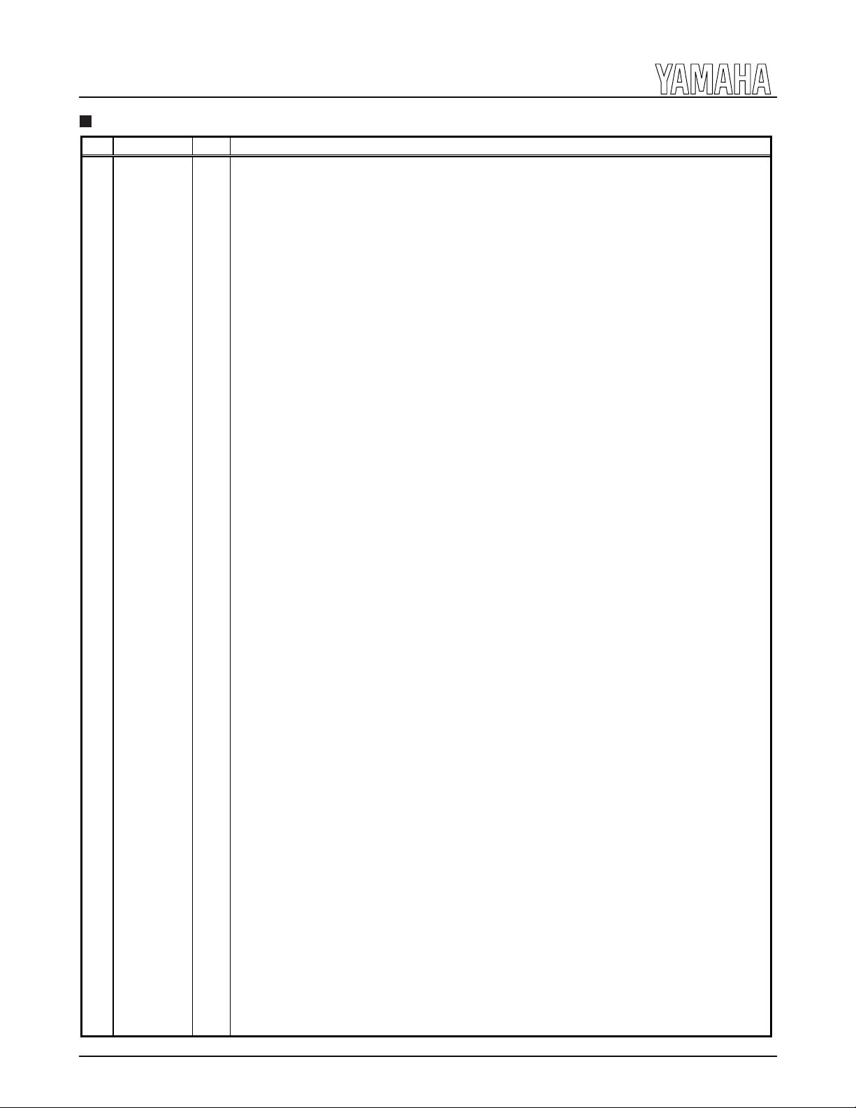
PIN FUNCTION
No. Name I/O FUNCTION
1 VDD1 - +5V power supply (for I/Os)
2 RAMCEN O External SRAM interface /CE
3 RAMA16 O External SRAM interface address 16
4 RAMA15 O External SRAM interface address 15
5SDIB0I+PCM in
6SDIB1I+PCM in
7SDIB2I+PCM in
8XI ICr
9XOOCr
10 VSS - Ground
11 AVDD - +3.3 V
12 SDIB3 I+ PCM in
13 TEST Test terminal
14 TEST Test terminal
15 OVFB O Detection of overflow at Sub DSP
16 DTSDATA O Detection of DTS data
17 AC3DATA O Detection of AC-3 data
18 SDOB3 O PCM out
19 CPO A Out
20 AVSS - Ground
21 VDD2 - +3.3 V
22 SDOA2 O PCM out
23 SDOA1 O PCM out
24 SDOA0 O PCM out
25 RAMA14 O External SRAM interface address 14
26 RAMA13 O External SRAM interface address 13
27 RAMA12 O External SRAM interface address 12
28 RAMA11 O External SRAM interface address 11
29 RAMA10 O External SRAM interface address 10
30 VSS - Ground
31 VDD1 - +5V
32 OPORT0 O Out
33 OPORT1 O Out
34 OPORT2 O Out
35 OPORT3 O Out
36 OPORT4 O Out
37 OPORT5 O Out
38 OPORT6 O Out
39 OPORT7 O Out
40 VSS - Ground
41 VDD2 - +3.3 V
42 RAMA9 O External SRAM interface address 9
43 RAMA8 O External SRAM interface address 8
44 RAMA7 O External SRAM interface address 7
45 SDOB2 O PCM out
46 SDOB1 O PCM out
47 SDOB0 O PCM out
48 SDBCK1 I+ Bit clock in
49 SDWCK1 I+ Word clock in
50 VSS - Ground
51 VDD2 - +3.3 V
52 NONPCM O Detection of non-PCM data
53 CRC O Detection of AC-3 CRC error
54 MUTE O Detection of auto mute
55 KARAOKE O Detection of AC-3 karaoke data
ut 0 to Sub DSP
ut 1 to Sub DSP
ut 2 to Sub DSP
stal oscillator connection (12.288 MHz
stal oscillator connection
ower supply (for PLL circuit
ut 3 to Sub DSP
to be open in normal use
to be open in normal use
ut from Sub DSP
ut terminal for PLL, to be connected to ground through the external analog filter circuit
for PLL circuit
ower supply (for core logic
ut from Main DSP (C, LFE
ut from Main DSP (LS, RS
ut from Main DSP (L, R
ower supply (for I/Os
ut port for general purpose
ut port for general purpose
ut port for general purpose
ut port for general purpose
ut port for general purpose
ut port for general purpose
ut port for general purpose
ut port for general purpose
ower supply (for core logic
ut from Sub DSP
ut from Sub DSP
ut from Sub DSP
ut for SDOA, SDIB, SDOB
ut for SDOA, SDIB, SDOB
ower supply (for core logic
3
Page 4
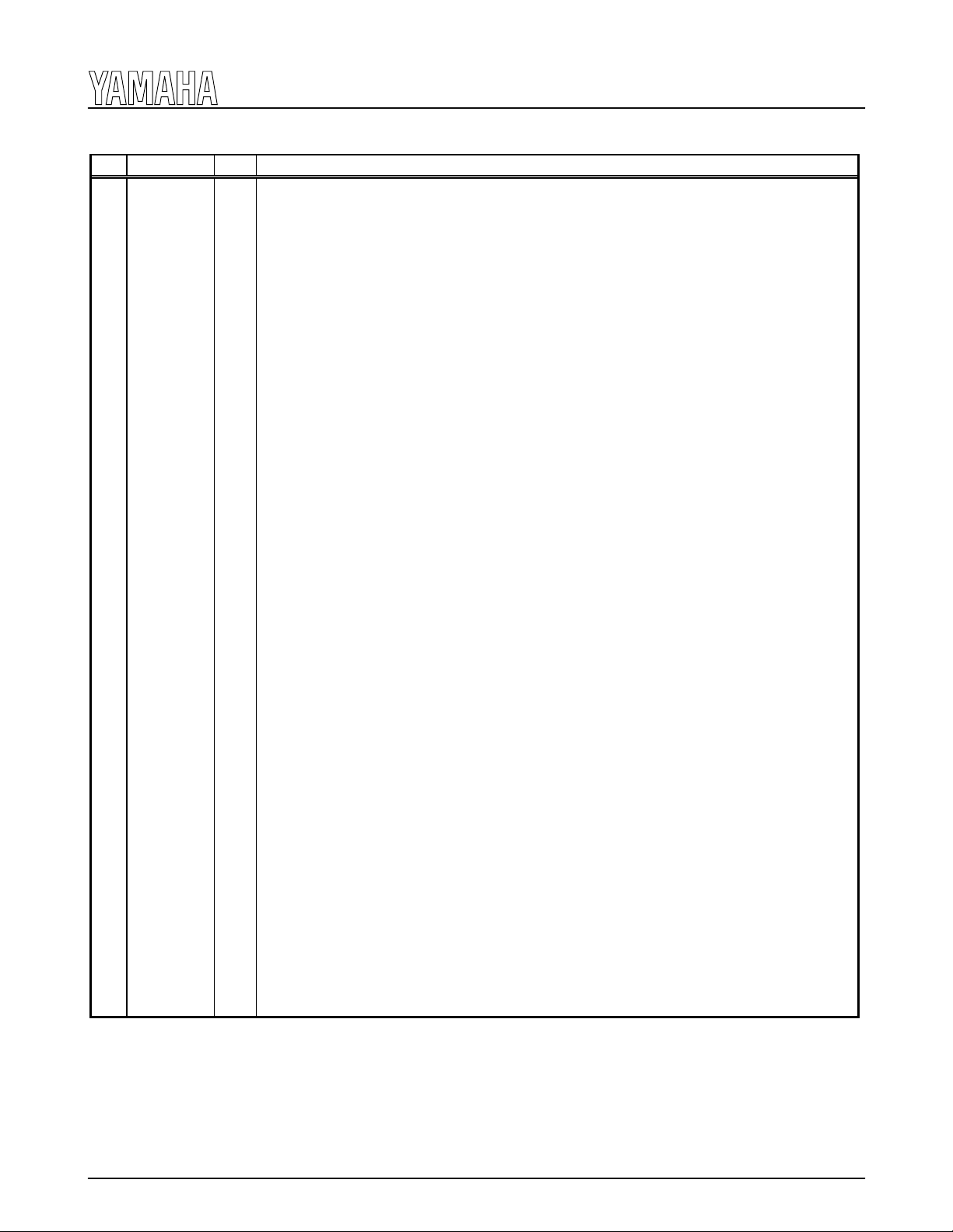
y
No. Name I/O FUNCTION
56 SURENC O Detection of AC-3 2/0 mode Dolb
57 /SDBCK0 O Inverted SDBCK0 clock output (refer to Block diagram)
58 RAMA6 O External SRAM interface address 6
59 RAMA5 O External SRAM interface address 5
60 VSS - Ground
61 RAMA4 O External SRAM interface address 4
62 /IC Is Initial clear
63 TEST Test terminal (to be open in normal use)
64 RAMA3 O External SRAM interface address 3
65 /CSB Is+ Sub DSP Chip select
66 /CS Is Microprocessor interface Chip select input
67 SO Ot Microprocessor interface Serial data output
68 SI Is Microprocessor interface / Sub DSP Serial data input
69 SCK Is Microprocessor interface / Sub DSP clock input
70 RAMA2 O External SRAM interface address 2
71 VDD1 - +5V power supply (for I/Os)
72 RAMD0 I+/ O External SRAM interface data (STREAM0 output when External SRAM is not in use)
73 RAMD1 I+/ O External SRAM interface data (STREAM1 output when External SRAM is not in use)
74 RAMD2 I+/ O External SRAM interface data (STREAM2 output when External SRAM is not in use)
75 RAMD3 I+/ O External SRAM interface data (STREAM3 output when External SRAM is not in use)
76 RAMD4 I+/ O External SRAM interface data (STREAM4 output when External SRAM is not in use)
77 RAMD5 I+/ O External SRAM interface data (STREAM5 output when External SRAM is not in use)
78 RAMD6 I+/ O External SRAM interface data (STREAM6 output when External SRAM is not in use)
79 RAMD7 I+/ O External SRAM interface data (STREAM7 output when External SRAM is not in use)
80 VSS - Ground
81 VDD2 - +3.3 V power supply (for core logic)
82 SDWCK0 I Word clock input for SDIA, SDOA, SDIB, SDOB
83 SDBCK0 I Bit clock input for SDIA, SDOA, SDIB, SDOB
84 SDIA0 I AC-3 bitstream (or PCM) data input for Main DSP
85 SDIA1 I AC-3 bitstream (or PCM) data input for Main DSP
86 RAMA1 O External SRAM interface address 1
87 RAMA0 O External SRAM interface address 0
88 RAMWEN O External SRAM interface /WE
89 RAMOEN O External SRAM interface /OE
90 VSS - Ground
91 VDD2 - +3.3 V power supply (for core logic)
92 IPORT7 I+ Input port for general purpose
93 IPORT6 I+ Input port for general purpose
94 IPORT5 I+ Input port for general purpose
95 IPORT4 I+ Input port for general purpose
96 IPORT3 I+ Input port for general purpose
97 IPORT2 I+ Input port for general purpose
98 IPORT1 I+ Input port for general purpose
99 IPORT0 I+ Input port for general purpose
100 VSS - Ground
surround encoded input
YSS912
NOTE) Is: Schmidt trigger input terminal
I+: Input terminal with a pull-up resistor
O: Digital output terminal
Ot: Tri-state digital output terminal
A: Analog terminal
4
Page 5
YSS912
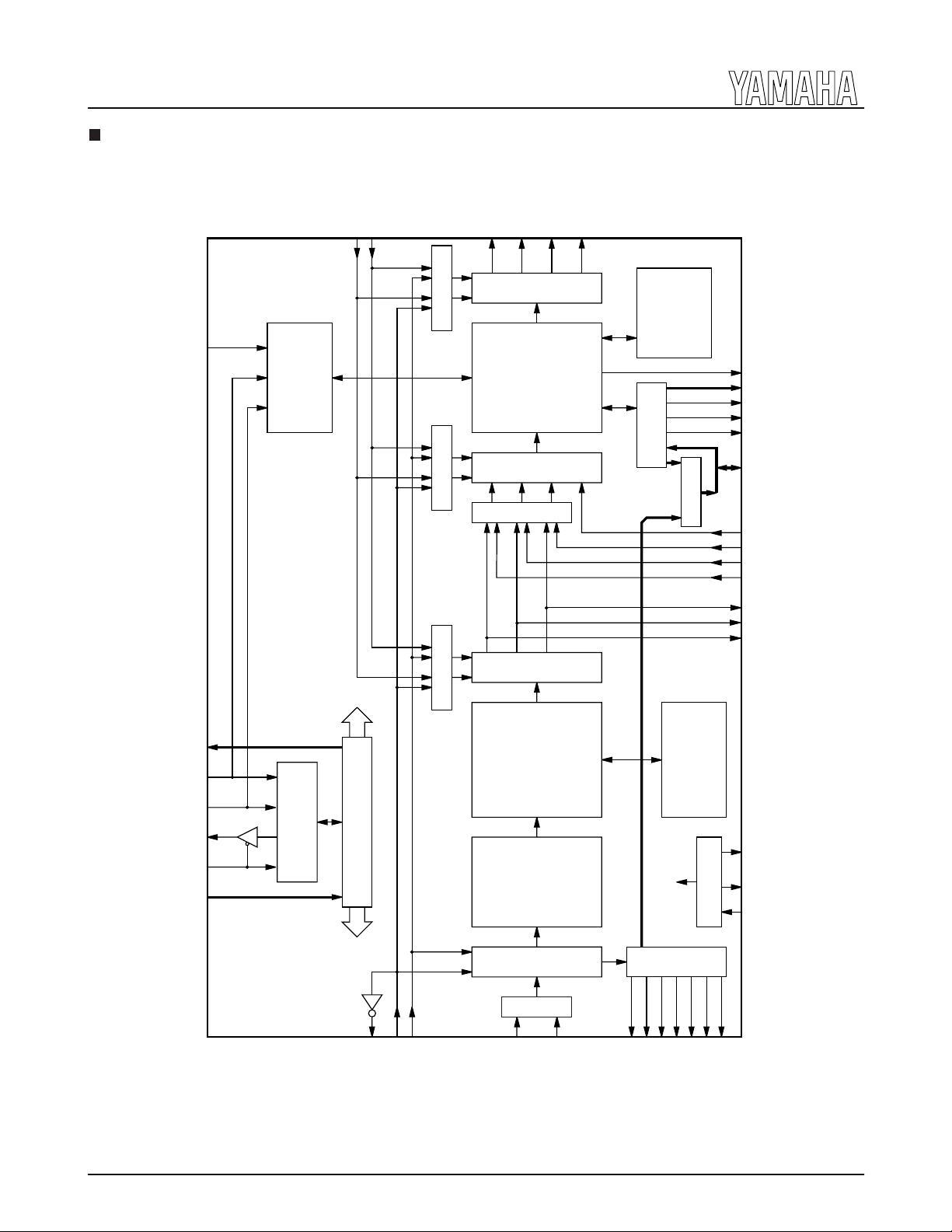
BLOCK DIAGRAM
/CSB
SCK
SI
Coefficient/
Program RAM
SDWCK1
SDBCK1
SDOB0
SDOB Interface
SDOBCKSEL
Sub DSP
SDIB Interface
SDIBSEL
LS, RS
L, R
SDOA Interface
SDOB1
24 * 16
C, LFE
SDOB2
SDOB3
Data RAM
interface
External RAM
ERAMUSE
OVFB
RAMA0 - 16
RAMOEN
RAMWEN
RAMCEN
RAMD0 - 7
SDIB3
SDIB2
SDIB1
SDIB0
SDOA2
SDOA1
SDOA0
OPORT0 - 7
SCK
SO
/CS
IPORT0 - 7
SDOACKSEL SDIBCKSEL
Control signals
24 * 24
Main DSP
AC-3/Pro Logic/DTS
SI
Interface
Microprocessor
Control Registers
decoder
Input Buffer
7
-
Delay RAM
(30MHz)
PLL
Operating clock
CPO
XO
XI
STREAM0
SDIA Interface
CRC
Control signals
SDIASEL
SDBCK0
/SDBCK0
SDWCK0
SDIA0
SDIA1
MUTE
SURENC
KARAOKE
CRC
AC3DATA
DTSDATA
NONPCM
5
Page 6

YSS912
FUNCTION DESCRIPTION
The YSS912 consist of Main DSP section where AC-3/Pro Logic/DTS decoding is executed and Sub DSP section
where various sound field effects are added. Please refer to “BLOCK DIAGRAM” section.
Sub DSP is a 8 ch input / 8 ch output programmable DSP exclusively for the sound field processing. It can apply
such effects as virtual surround, echo and equalizing. In addition, with an SRAM up to 1Mbit connected, it can
produce reverberation for one second or longer. By using this function, it is possible to simulate various sound
fields such as a hall or a church.
* If adopting some technology owned by another company is desired for use in Sub DSP section, note that a separate
contract may be required between the owner of that technology and the user with respect to adoption of the
technology.
1. Clocks XI, XO, CPO
The crystal oscillation circuit is formed by using XI and XO terminals.
Connect a crystal of 12.288 MHz between XI and XO terminals.
Connect an external analog filter between CPO terminal and Ground.
2. Data Interface SDIA0, SDIA1, SDOA0-2, SDIB0-3, SDOB0-3, SDWCK0, SDBCK0,
SDWCK1, SDBCK1, /SDBCK0
Main DSP section
AC-3/PCM/DTS data should be fed from SDIA0 or SDIA1 terminal. These signals are processed by AC-3/Pro
Logic/DTS decoding procedure in Main DSP section and then transmitted to Sub DSP section as well as
outputted through SDOA0-2 terminals.
Sub DSP section
In Sub DSP section, various types of processing can be applied to the PCM data decoded in Main DSP section or
inputted through SDIB0 - 3 terminals. Then, processed signals are outputted from each of SDOB0-3 terminals.
Following parameters can be selected by changing the control register setting.
.
Selection of Main DSP input signal (SDIA0, SDIA1)
.
Selection of Sub DSP input signal (Main DSP output, SDIB0-3 input)
.
Polarity of bit clock and word clock
.
Format and bit count of input/output data
For more information on the format of the input/output data, please refer to “Serial Data Interface” section.
3. Microprocessor Interface /CS, /CSB, SCK, SI, SO
The control registers can be read/written via the serial microprocessor interface by using /CS, SCK, SI, and SO
terminals.
Please refer to the following format diagram for the details of read/write timing.
6
Page 7

YSS912
Format diagram for read/write timing
When /CS=1, the SO output becomes high-impedance.
* Be sure to set /CSB to “1” when making an access to the control register.
The sound field processing program used for Sub DSP is down-loaded by using the /CSB, SCK, and SI terminals.
Please refer to Application manual for the details of Sub DSP.
4. External Interface RAMA0-16, RAMD0-7, RAMCEN, RAMOEN, RAMWEN
An external SRAM can be connected to Sub DSP.
5. General purpose I/O ports OPORT0-7, IPORT0-7
OPORT0-7 terminals are output ports for general purpose. Data w ritten on the register (address 0x04) are outputted
from these terminals.
IPORT0-7 terminals are input ports for general purpose. Data inputted to these terminals can be read from the
register (address 0x05).
6. Initial clear /IC
This LSI requires initial clear when turning on the power.
7. LSI test terminals TEST
Leave the test terminals open in normal use.
7
Page 8

s
y
YSS912
CONTROL REGISTER
The decoding system is controlled by reading and writing the control registers through microprocessor interface
(/CS, SCK, SI and SO).
Note : All bits are set to “0” by initial clear (/IC=0) except bit 4 of PLL/DSN register (0x00).
addres
0x00
0x01
0x02
0x03
0x04
0x05
0x09
0x0A
0x0B
0x0C
0x0D
0x0E
0x0F
0x10
0x11
0x12
0x13
0x14
0x15
0x16
0x17
PLL/DSN Register PLLUSE (not used) DSNIGN DSN2 - 0
Mute Register LMUTEN CMUTEN RMUTEN RSMUTEN LSMUTEN
SDIA Register SDIASEL PDOWN SDIAFMT1 - 0 SDIABIT1 - 0 SDIAWP SDIABP
SDOA Register
OPORT Register OPORT7 - 0
IPORT Register IPORT7 - 0 (Read only)
Noise Level Register NOISELEV7 - 0
Center Delay Register
S
Noise Register NOISE PN/WN IMPULSE
FS Register
L Volume Register LVOL7 - 0
C Volume Register CVOL7 - 0
R Volume Register RVOL7 - 0
LS Volume Register LSVOL7 - 0
RS Volume Register RSVOL7 - 0
LFE Volume Register LFEVOL7 - 0
Compression Register EMPON AIBON VOLON DITHOFF P11OFF DIALOFF COMPMOD1 - 0
HDYNRNG Register HDYNRNG7 - 0
LDYNRNG Register LDYNRNG7 - 0
Mode Register PCM PLDECON PLSRMOD DUALMOD1 - 0 OUTMOD2 - 0
Name bit 7 bit 6 bit 5 bit 4 bit 3 bit 2 bit 1 bit 0
LFEMUTEN DSPMUTEN
SDOACKSEL
urround Delay Register
SDOAFMT1 - 0 SDOABIT1 - 0 SDOAWP SDOABP
CDELAY2 - 0
SRDELAY3 - 0
AMOFF
FS1 - 0
COEF0-H Register COEF0-15 - 8
0x30
COEF0-L Register COEF0-7 - 0
0x31
COEF1-H Register COEF1-15 - 8
0x32
COEF1-L Register COEF1-7 - 0
0x33
SDIB Register SDIBCKSEL SDIBSEL SDIBFMT1 - 0 SDIBBIT1 - 0 SDIBWP SDIBBP
0x34
SDOB Register
0x35
ERAM Register ERAMUSE MPCNT5 - 0
0x36
Note : Do not write "1" into the cross-hatched bits because the
SDOBCKSEL
SDBUSE SDOBFMT1 - 0 SDOBBIT1 - 0 S DOBWP SDOBBP
are used for testing the LSI.
8
Page 9

YSS912
s
The following registers of address 0x18 to 0x2F are read-only (write disabled).
The contents of the registers of address 0x18 to 0x2A vary depending on input signal, AC-3 bitstream, DTS bitstream
or PCM, as described below.
1) When input signal is AC-3 bitstream
addres
0x18
0x19
0x1A
0x1B
0x1C
0x1D
0x1E
0x1F
0x20
0x21
0x22
0x23
0x24
0x25
0x26
0x27
0x28
0x29
0x2A
Bitstream Register 0
Bitstream Register 1
Bitstream Register 2
Bitstream Register 3
Bitstream Register 4
Bitstream Register 5
Bitstream Register 6
Bitstream Register 7
Bitstream Register 8
Bitstream Register 9
Bitstream Register 10
Bitstream Register 11
Bitstream Register 12
Bitstream Register 13
Bitstream Register 14
Bitstream Register 15
Bitstream Register 16
Bitstream Register 17
Bitstream Register 18
Name bit 7 bit 6 bit 5 bit 4 bit 3 bit 2 bit 1 bit 0
fscod frmsizecod
bsid bsmod
acmod cmixlev surmixlev lfeon
dsurmod copyrightb origbs 0 0 0 0
0 0 0 dialnorm
0 0 0 dialnorm2
audprodie mixlevel roomtyp
audprodi2e mixlevel2 roomtyp2
timecod1e 0 timecod1
timecod1
timecod2e 0 timecod2
timecod2
langcode langcod2e compre compr2e 0 0 0 0
langcod
langcod2
compr
compr2
dynrng
dynrng2
2) When input signal is DTS bitstream
address
0x18
0x19
0x1A
0x1B
Bitstream Register 0
Bitstream Register 1 undefined
Bitstream Register 2 AMODE undefined lfeon
Bitstream Register 3
Name bit 7 bit 6 bit 5 bit 4 bit 3 bit 2 bit 1 bit 0
fscod
undefined RATE
undefined
The contents of registers of address 0x1C to 0x2A are undefined.
3) When input signal is PCM
The contents of registers of address 0x18 to 0x2A are undefined.
The registers of address 0x2B, 0x2C are not used.
From the registers of address 0x2D to 0x2F, the following data can be read.
address
0x2D
0x2E
0x2F
Pc Register undefined
Data Stream Register
Status Register
Name bit 7 bit 6 bit 5 bit 4 bit 3 bit 2 bit 1 bit 0
Pc4 - 0
STREAM7 STREAM6 STREAM5 STREAM4 STREAM3 STREAM2 STREAM1 STREAM0
DTSDATA AC3DATA 2/0MODE SURENC
KARAOKE
MUTE CRC NONPCM
Address 0x06 to 0x08 and 0x37 to 0x7F are assigned for TEST. Never access to these registers.
Please refer to Application manual for details of Control register.
PCMR
9
Page 10

SERIAL DATA INTERFACE
Data timing of the serial data interface is as follows.
YSS912
Please refer to Application manual for details of SDIA, SDOA, SDIB, and SDOB registers.
10
Page 11

YSS912
ELECTRICAL CHARACTERISTICS
1. Absolute Maximum Ratings
Parameter Symbol Min. Max. Unit
Power Supply Voltage V
Input Voltage V
Storage Temperature T
DD1
V
, AV
DD2
I
stg
2. Recommended Operating Conditions
Parameter Symbol Min. Typ. Max. Unit
Power Supply Voltage V
Operating Temperature T
V
DD2
DD1
, AV
op
3. DC Characteristics (Condition: Under Recommended Operating Conditions)
Parameter Symbol Condition Min. Typ. Max. Unit
Input Voltage H Level (1) V
Input Voltage H Level (2) V
Input Voltage L Level (1) V
Input Voltage L Level (2) V
Output Voltage H Level V
Output Voltage L Level V
Input Leakage Current I
Pull-up Resistor R
Power Consumption P
IH1
IH2
IL1
IL2
OH
OLIOL
LI
U
D
*1 Applicable to XI and /IC input terminals.
*2 Applicable to input terminals except XI and /IC terminals.
Vss-0.5 Vss+7.0 V
Vss-0.5 VSS+4.6 V
DD
Vss-0.5 V
-50 125
+0.5 V
DD1
C
4.75 5.0 5.25 V
DD
3. 0 3.3 3.6 V
02570
*1 0.7V
*2 2.2 V
*1 0.2V
*2 0.8 V
IOH = -80 mA
V
DD1
= 1.6 mA 0.4 V
Terminal without a pull-up
-10 10
resistor
25 100
C
DD1
DD1
-1.0 V
400 550 mW
V
V
A
m
k
W
4. XI and /IC
XI clock frequency X
XI clock duty X
/IC pulse width
Parameter Symbol Conditions Min Typ Max Unit
12.288 MHz
duty
t
icw
in
40 50 60 %
Power voltage to be stabilized 500 ns
11
Page 12

EXTERNAL DIMENSIONS
80
YSS912
C-PK100FP-1
24.80 0.40
20.00 0.30
0.15 0.05
(LEAD THICKNESS)
51
81
100
P-0.65TYP
2.95 MAX.
50
14.00 0.30
18.80 0.40
31
1
0.30
30
0.10
(2.40)
0-15
12
0 MIN.
(STAND OFF)
The figure in the parenthesis ( )
should be used as a reference.
Plastic body dimensions do not
include burr of resin.
UNIT: mm
1.20
0.20
Page 13

YSS912
13
Page 14

r
YSS912
IMPORTANT NOTICE
1. Yamaha reserves the right to make changes to its Products and to this document
without notice. Th e information contained in this docume nt has been carefull y checked
and is believed to be reliable. However, Yamaha assumes no responsibilities fo
inaccuracies and makes no commitment to update or to keep current the information
contained in this document.
2. These Yamaha Products are designed only for commercial and normal industrial
applications, and are not suitable for other uses, such as medical life support equipment,
nuclear facilities, critical care eq uipment or any other application the failure of wh ich could
lead to death, personal injury or environmental or property damage. Use of the Products
in any such application is at the customer's sole risk and expense.
3. YAMAHA ASSUMES NO LIABILITY FOR INCIDENTAL, CONSEQUENTIAL OR
SPECIAL DAMAGES OR INJURY T HAT MAY RESULT FROM MISAPPLICATION OR
IMPROPER USE OR OPERATION O F THE PRO DUCTS.
4. YAMAHA MAKES NO WARRANTY OR RE PRESEN TAT ION THAT THE PRODU CT S
ARE SUBJECT TO INTELLECTU AL PROPERTY LICENSE FROM YA MAHA OR
ANYTHIRD PARTY, AND YAMAHA MAKES NO WARRANTY OR REPRESENTATION
OF NON-INFRINGEMENT WITH RESPECT TO THE PRODUCTS. YAMAHA
SPECIFICALLY EXCLUDES ANY LIABILITY TO THE CUSTOMER OR ANY THIRD
PARTY ARISING FROM OR R E LATE D TO TH E PR ODU CT S' IN FRIN GEMEN T OF A NY
THIRD PARTY'S INTELLECTUAL PROPERTY RIGHTS, INCLUDING THE PATENT,
COPYRIGHT, TRADEMARK OR TRADE SECRET RIG HTS OF ANY THIRD PARTY.
5. EXAMPLES OF USE DESCRIBED HEREIN ARE MERELY TO INDICATE THE
CHARACTERISTICS AND PERFORMANCE OF YAMAHA PRODUCTS. YAMAHA
ASSUMES NO RESPONSIBILITY F OR A NY INTE LL ECTUA L PR OPER TY CLAIMS OR
OTHER PROBLEMS THAT MAY RESULT FROM APPLICATIONS BASED ON THE
EXAMPLES DESCRIBED HEREIN. YAMAHA MAKES NO WARRANTY W ITH
RESPECT TO THE PRODUCTS, EXPRESS OR IMPLIED, INCLUDING, BUT NOT
LIMITED TO THE WARRANTIES OF MERCHANTABILITY, FITNESS FOR A
PARTICULAR USE AND TITLE.
Note) The specifications of this product are subject to improvement change without prior notice.
AGENCY
Address inquiries to:
Semi-conductor Sales & Marketing Department
YAMAHA CORPORATION
Head Office
Tokyo Office
Osaka Office
U.S.A Office
203, Matsunokijima, Toyooka-mura,
Iwata-gun, Shizuoka-ken,438-0192
Tel. +81-539-62-4918
2-17-11, Takanawa, Minato-ku, Tokyo, 108-8568
Tel. +81-3-5488-5431
Nanba Tsujimoto Nissei Bldg. 4F
1-13-17, Nanba-naka, Naniwa-ku
Osaka City, Osaka, 556-0011
Tel. +81-6-633-3690
YAMAHA Systems Technology.
100 Century Center Court, San Jose, CA 95112
Tel. +1-408-467-2300
Fax. +81-539-62-5054
Fax. +81-3-5488-5088
Fax. +81-6-633-3691
Fax. +1-408-437-8791
COPYING PROHIBITED © 1987
YAMAHA CORPORATION
Printed in Japan
 Loading...