YSS902
AC3D
Dolby Digital (AC-3) / Pro Logic decoder + Sub DSP
YSS902 CATALOG
CATALOG No.:LSI-4SS902A4
1999. 7
INTRODUCTION
The YSS902 is one chip LSI consisting of two built-in DSP’s ; Dolby Digital (AC-3) / Pro L ogic (Main DSP) and a
sound processing DSP (Sub DSP). Sub DSP is capable of realizing various sound fields, such as virtual surround, by
down-loading the program and coefficient.
FEATURERS
Dolby Digital 5.1 channel full decode.
24 bit DSP. (Group-A Dolby Digital decoder)
No external memory is required. (Memories for center and surround channel delay are included)
Possible to decode multi-language encoded data. (possible to decode based on data-stream-number)
AC-3 karaoke mode.
Original compression modes as well as four compression modes recommended by Dolby.
Dolby Digital decoding latency is fixed to two audio blocks (512 samples).
Included de-emphasis filter.
Pro Logic decoding for Dolby Digital 2 channels decoded signal as well as ordinary PCM.
High performance 25 MIPS programmable DSP suitable for a variety of sound field processing such as original
surround, filtering, virtual surround etc.
Up to 1.36 second delay time is capable when used with an external 1Mbit SRAM. (at fs= 48 kHz)
Reads Dolby Digital decode information through the microprocessor interface.
Provide total sixteen I/O ports.
Possible to connect most of SPDIF receivers, A/D and D/A converters, by setting I/O data interface format.
Has a built-in PLL oscillation circuit to generates its own operating clock.
Internal operating clock is 25MHz.
Supply Voltage: 3.3v for core logic. 5v for I/Os.
Power saving mode.
Si-gate CMOS process.
100 QFP.(YSS902-F)
Note: "AC-3" and "Pro Logic" are registered trademarks of Dolby Laboratories Licensing Corporation.
Use of this LSI must be licensed by Dolby Laboratories Licensing Corporation.

YSS902
2
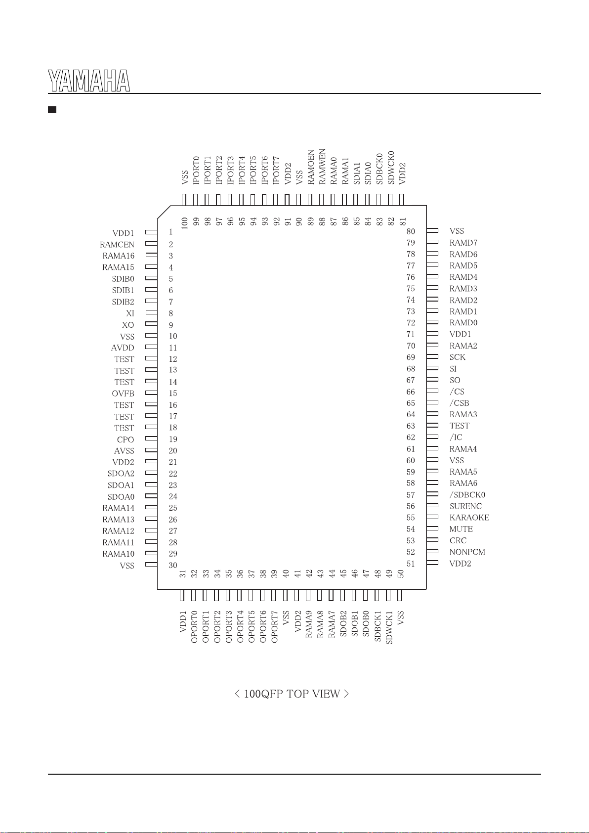
PIN CONFIGURATION

YSS902
3
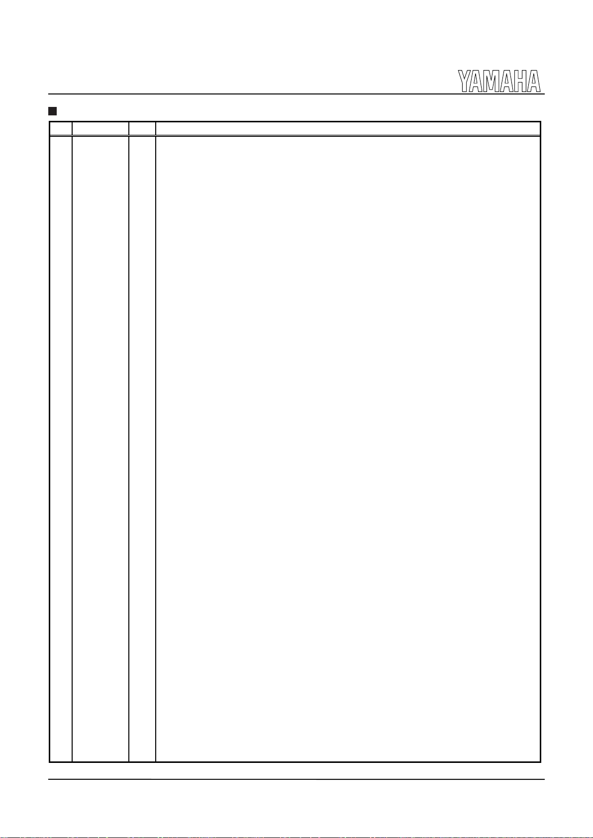
PIN FUNCTION
No. Name I/O FUNCTION
1 VDD1 - +5V power supply (for I/Os)
2 RAMCEN O External SRAM interface /CE
3 RAMA16 O External SRAM interface address 16
4 RAMA15 O External SRAM interface address 15
5SDIB0I+PCM input 0 to Sub DSP
6SDIB1I+PCM input 1 to Sub DSP
7SDIB2I+PCM input 2 to Sub DSP
8XI ICr
y
stal oscillator connection (6.125MHz - 50.0MHz
)
9XOOCr
y
stal oscillator connection
10 VSS - Ground
11 AVDD - +3.3 V power supply (for PLL circuit
)
12 TEST Test terminal (to be open in normal use
)
13 TEST Test terminal (to be open in normal use
)
14 TEST Test terminal (to be open in normal use
)
15 OVFB O Detection of overflow at Sub DSP
16 TEST Test terminal (to be open in normal use
)
17 TEST Test terminal (to be open in normal use
)
18 TEST Test terminal (to be open in normal use
)
19 CPO A Output terminal for PLL, to be connected to ground through the external analog filter circuit
20 AVSS - Ground (for PLL circuit
)
21 VDD2 - +3.3 V power supply (for core logic
)
22 SDOA2 O PCM output from Main DSP (C, LFE
)
23 SDOA1 O PCM output from Main DSP (LS, RS
)
24 SDOA0 O PCM output from Main DSP (L, R
)
25 RAMA14 O External SRAM interface address 14
26 RAMA13 O External SRAM interface address 13
27 RAMA12 O External SRAM interface address 12
28 RAMA11 O External SRAM interface address 11
29 RAMA10 O External SRAM interface address 10
30 VSS - Ground
31 VDD1 - +5V power supply (for I/Os
)
32 OPORT0 O Output port for general purpose
33 OPORT1 O Output port for general purpose
34 OPORT2 O Output port for general purpose
35 OPORT3 O Output port for general purpose
36 OPORT4 O Output port for general purpose
37 OPORT5 O Output port for general purpose
38 OPORT6 O Output port for general purpose
39 OPORT7 O Output port for general purpose
40 VSS - Ground
41 VDD2 - +3.3 V power supply (for core logic
)
42 RAMA9 O External SRAM interface address 9
43 RAMA8 O External SRAM interface address 8
44 RAMA7 O External SRAM interface address 7
45 SDOB2 O PCM output from Sub DSP
46 SDOB1 O PCM output from Sub DSP
47 SDOB0 O PCM output from Sub DSP
48 SDBCK1 I+ Bit clock input for SDOA, SDIB, SDOB
49 SDWCK1 I+ Word clock input for SDOA, SDIB, SDOB
50 VSS - Ground
51 VDD2 - +3.3 V power supply (for core logic
)
52 NONPCM O Detection of non-PCM data
53 CRC O Detection of CRC error
54 MUTE O Detection of auto mute
55 KARAOKE O Detection of AC-3 karaoke data

YSS902
4
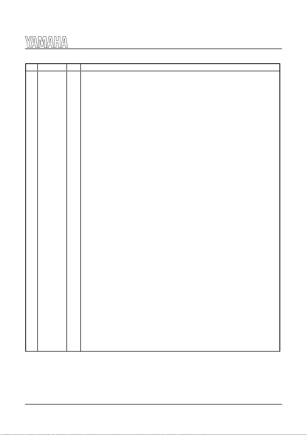
No. Name I/O FUNCTION
56 SURENC O Detection of AC-3 2/0 mode Dolby surround encoded input
57 /SDBCK0 O Inverted SDBCK0 clock output (refer to Block diagram)
58 RAMA6 O External SRAM interface address 6
59 RAMA5 O External SRAM interface address 5
60 VSS - Ground
61 RAMA4 O External SRAM interface address 4
62 /IC Is Initial clear
63 TEST Test terminal (to be open in normal use)
64 RAMA3 O External SRAM interface address 3
65 /CSB Is+ Sub DSP Chip select
66 /CS Is Microprocessor interface Chip select input
67 SO Ot Microprocessor interface Serial data output
68 SI Is Microprocessor interface / Sub DSP Serial data input
69 SCK Is Microprocessor interface / Sub DSP clock input
70 RAMA2 O External SRAM interface address 2
71 VDD1 - +5V power supply (for I/Os)
72 RAMD0 I+/ O External SRAM interface data (STREAM0 output when External SRAM is not in use)
73 RAMD1 I+/ O External SRAM interface data (STREAM1 output when External SRAM is not in use)
74 RAMD2 I+/ O External SRAM interface data (STREAM2 output when External SRAM is not in use)
75 RAMD3 I+/ O External SRAM interface data (STREAM3 output when External SRAM is not in use)
76 RAMD4 I+/ O External SRAM interface data (STREAM4 output when External SRAM is not in use)
77 RAMD5 I+/ O External SRAM interface data (STREAM5 output when External SRAM is not in use)
78 RAMD6 I+/ O External SRAM interface data (STREAM6 output when External SRAM is not in use)
79 RAMD7 I+/ O External SRAM interface data (STREAM7 output when External SRAM is not in use)
80 VSS - Ground
81 VDD2 - +3.3 V power supply (for core logic)
82 SDWCK0 I Word clock input for SDIA, SDOA, SDIB, SDOB
83 SDBCK0 I Bit clock input for SDIA, SDOA, SDIB, SDOB
84 SDIA0 I AC-3 bitstream (or PCM) data input for Main DSP
85 SDIA1 I AC-3 bitstream (or PCM) data input for Main DSP
86 RAMA1 O External SRAM interface address 1
87 RAMA0 O External SRAM interface address 0
88 RAMWEN O External SRAM interface /WE
89 RAMOEN O External SRAM interface /OE
90 VSS - Ground
91 VDD2 - +3.3 V power supply (for core logic)
92 IPORT7 I+ Input port for general purpose
93 IPORT6 I+ Input port for general purpose
94 IPORT5 I+ Input port for general purpose
95 IPORT4 I+ Input port for general purpose
96 IPORT3 I+ Input port for general purpose
97 IPORT2 I+ Input port for general purpose
98 IPORT1 I+ Input port for general purpose
99 IPORT0 I+ Input port for general purpose
100 VSS - Ground
NOTE) Is: Schmidt trigger input terminal
I+: Input terminal with a pull-up resistor
O: Digital output terminal
Ot: Tri-state digital output terminal
A: Analog terminal
 Loading...