

YAMAHA YSS901 Datasheet
YSS901
SD
Preliminary
Stereo dipole
Outline
g
YSS901 is a device that uses the stereo dipole system (SD) with which the transaural system can be constructed.
When a stereophonic signal that has been processed with the SD system of this device is inputted to two
speakers located adjacently at the center of the field (or to two speakers contained in one cabinet), the virtual
sound positioning function of this system produces the stereophonic sound similar to the one that can be
obtained by using an ordinary stereophonic sound replay system through the central two speakers.
YSS901 has built-in one bit Delta-Sigma type A/D and D/A converters for each of the two channels at its input
and output respectively. Thanks to these built-in converters, this device can process analog stereophonic sound
signal through the converters in addition to digital stereophonic sound signal.
This device performs an advanced convolution through DSP using the FIR filter.
Features
g
Two channel virtual sound positioning by using the stereo dipole system.
n
Processes analog or digital signals at each of the two channels.
n
Four types of digital data format are available, including 48 fs Serial-DAC16, 18 and 20 bits, and 64 fs.
n
Six types of parameter coefficients are built in the device. Additional parameter coefficients can be
n
downloaded externally.
The parameter control is made through the DC switches or synchronous three-wire serial system.
n
Uses a clock of 2.822 MHz from the crystal. External clock can also be used.
n
Has a built-in PLL circuit for generating clock for operation.
n
Internal operating frequency of 512 fs.
n
Allows fading in or out the output of the results of the convolution when switching the coefficient.
n
Power supply voltage: 5 V
n
Si-gate CMOS process.
n
64 QFP
n
YAMAHA CORPORATION
YSS901CATALOG
CATALOG No.: LSI-4SS901A0
1999. 1
Pin configuration
g
N.C
N.CN.C
32
AVDD
31
VREF
30
AIL
29
AILRET
AILOUT
27
28
AIR
26
AIRRET
AIROUT
24
25
AVSS
23
DVSS
22
TST2
21
N.CN.C
20
YSS901
N.C
N.C
N.C
N.C
LOUT
ROUT
PLLC
EXTAL
XTAL
DVSS
TSTCK
TST1
TSTNI
TSTNO
N.C
N.C
N.C N.C
N.C
343536373839404142
43 33
4445464748495051
52
53
54
55
56
YSS901
57
58
59
60
61
62
63
12 13 14 15 16 17 18 19
1234567891011
64
N.C
N.C
N.C
DVDD
DSEL0
DSEL1
DSEL2AVSS
DIN
DOUT
CSN
BCLK
SYNCN
CTLSEL
DVDD
N.C
N.C
N.C
DVDD
CSEL2
TSTSEL
CSEL1
CSEL0
BSFT1
RESETN
BSFT0
<64QFP TOP VIEW>
2
SCK
SI
DVSS

YSS901
Pin Description
g
No. Pin name I/O
5 DVDD
CTLSEL I Selection of control method
6
7 SYNCN I Digital input/output synchronization signal
8 BCLK
9
CSN
10 DOUT
11
12 DSEL2
13 DSEL1
14 DSEL0
15 DVDD
21 TST2
22 DVSS
23 AVSS
24
25
26
27
28
29
30 VREF
31 AVDD
37 LOUT AO Left channel analog signal outp ut
38 ROUT AO Right channel analog signal output
39 PLLC
40 AVSS
41 EXTAL
42 XTAL
43 DVSS
44 TSTCK
45 TST1
46 TSTNI
47 TSTNO O Test (To be open.)
53 DVDD
54
55 CSEL2
56 CSEL1
57 CSEL0
58 RESETN I Reset signal input
59 BSFT1
60 BSFT0
61
62
63 DVSS
DIN
AIRRET AO Right channel analog signal input return
AIROUT AO Right channel analog signal input out
AIR
AILRET AO Left channel analog signal input return
AILOUT AO Left channel analog signal input out
AIL
TSTSEL - Test (Connect with DVSS.)
SCK
SI
Digital signal power supply : +5 V
-
Digital input/output bit clock
I
Serial control interface chip select signal
I
Digital signal output
O
Digital signal input
I
Analog/digital input selection
I
Digital input/output format selection
I
Digital input/output format selection
I
Digital signal power supply : +5 V
-
Test (To be open.)
-
- Digital signal ground
Analog signal ground
-
Right channel analog signal input
AI
Left channel analog signal input
AI
Analog signal VREF
AI
Analog signal power supply : +5 V
-
PLL auxiliary input
AI
Analog signal ground
-
Crystal clock input
I
Crystal clock output
O
Digital signal ground
-
Test (Connect with DVSS.)
-
Test (To be open.)
-
Test (Connect with DVSS.)
I
Digital signal power supply: +5 V
-
Coefficient selection (Enabled when CTLSEL = 0)
I
Coefficient selection (Enabled when CTLSEL = 0)
I
Coefficient selection (Enabled when CTLSEL = 0)
I
Bit shift selection (Enabled when CTLSEL = 0)
I
Bit shift selection (Enabled when CTLSEL = 0)
I
Serial control interface clock input
I
Serial control interface data input
I
Digital signal ground
-
Function
Notes:
1. Pins of No. 1 to 4, 16 to 20, 32 to 36, 48 to 52 and 64 are to be open.
2. I: input pin
O: output pin
AI: analog signal input pin
AO: analog output pin.
3
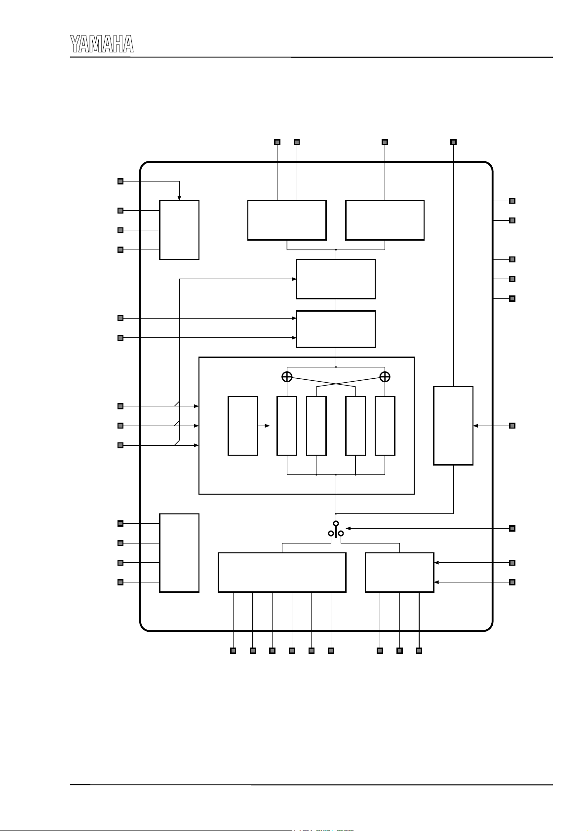
Block Diagram
g
CTLSEL
LOUT
ROUT
DOUT
YSS901
NGO
SI
SCK
CSN
BSFT1
BSFT0
CSEL2
CSEL1
CSEL0
Serial
Control
COEF
stereo dipole
Lch
Lch
DA
COEF 1
COEF 2
Lch
Fader
Bit
Shift
COEF 2
Rch
Digital
Out
Rch
COEF 1
Rch
Noise Gate
(Input Level Check)
DVDD
DVSS
AVDD
AVSS
VREF
NGATE
PLLC
EXTAL
XTAL
RESETN
4
Timing
AIL
AILRET
AILOUT
AD
AIR
AIROUT
AIRRET
Digital
SYNCN
In
BCLK
DSEL2
DSEL1
DSEL0
DIN
YSS901
Outline of Functions
g
1. Clock signals
For the clock signal, use the crystal connected to XTAL EXTAL pin with which the clock signal is obtained by the
self-oscillation at the cr ystal osc illatio n cir cuit, o r e xternal signa l supp lied thr o ugh EXT AL p in. The frequency of the
clock obtained by the self-oscillation is 2.822 MHz (or 44.1 kHz * 64). The internal operation is carried out with 512
fs clock that is made by the PLL.
Insert an analog filter in between PLLC and GND pins.
XTAL, EXTAL
2. Data input/output signals
and
PLLC
Analog/digital input selection pin:
This pin is used to select a type of the input signal. DSEL2 = 0 selects the digital signal input, or DSEL2 = 1 selects
the analog signal input.
DSEL2
2-1) Digital signal
Digital signal input/output pins:
Digital signals should be inputte d through DIN, BCLK and SYNCN pins.
DIN signal (PCM data) must be in synchronous with BCLK (bit clock) and SYNCN (word clock) signals.
Digital signal is outputted from DOUT pin.
Input/output format designation pins:
These pins are used to designate a data format for DAC. The settings of DSEL1 and DSEL0 and their output formats
are as follows.
DSEL1 DSEL0
00
01
10
11
DAC output format
48 fs 16 bits Data LSB justified
48 fs 18 bits Data LSB justified (Bits 1 and 0 are “0”.)
48 fs 20 bits Data LSB justified (Bits 3 through 0 are “0”.)
64 fs 16 bits Data MSB justified (Delay by one bit)
DIN, BCLK, SYNCN
DSEL1
and
and
DSEL0
DOUT
For the details of the format, refer to “Serial Data Interface” explained later in this document.
2-2) Analog signal
Analog input/output pins:
Analog signals should b e inputted through AIL and AI R pins. The signals that have been processed by the stereo
dipole (SD) are outputted from LOUT and ROUT pins respectively. Add an analog filter circuit, an example of
which is shown later in this document.
Center voltage pin
This pin outputs a reference voltage for analog signal processing. Connect an appropriate capacitor between VREF
and GND pins.
AIL, AILOUT, AILRET, LOUT, AIR, AIROUT, AIRRET
VREF
and
3. Controlling functions
3-1) Control method selection pin:
CTLSEL
This pin is used for selection of a control method as described below.
CTLSEL = 0 : Selection of CSEL2, CSEL1 or CSEL0 by means of DC switch (H/L) is enabled.
CTLSEL = 1 : Selection of CSN, SI or SCK through the microcomputer is enabled.
ROUT
5
 Loading...