

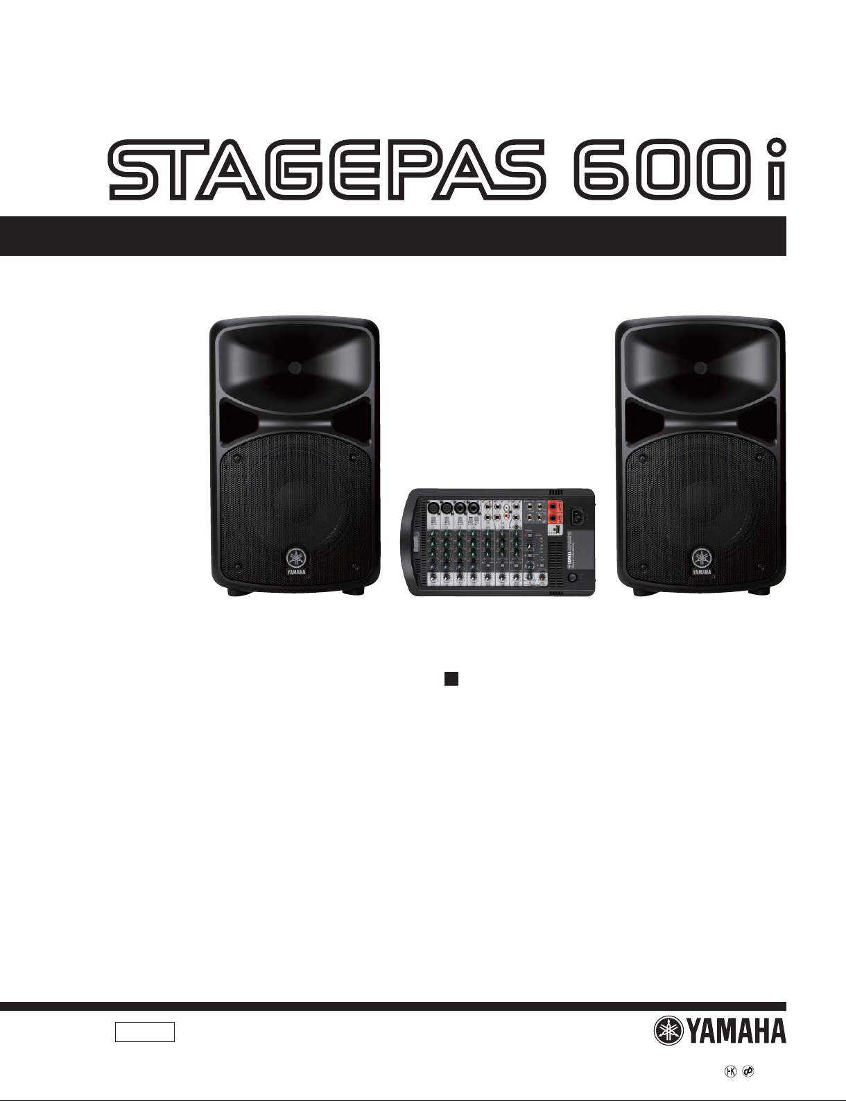
PORTABLE PA SYSTEM
SERVICE MANUAL
SPEAKER
MIXER
SPEAKER
CONTENTS(目次)
SPECIFICATIONS(総合仕様) .................................. 3/4
PANE L L AYOUT(パネルレイアウト) ............................5
CIRCUIT BOARD LAYOUT(ユニットレイアウト) ......... 6
DIMENSIONS(寸法図) ...............................................7
DISASSEMBLY PROCEDURE(分解手順) .................. 8
LSI PIN DESCRIPTION(LSI 端子機能表) ................. 2 2
CIRCUIT BOARDS(シート基板図) ............................ 25
TEST PROGRAM(テストプログラム) ......................... 34
INSPECTIONS(検査) ................................................ 52
UPDATING(アップデート) .......................................... 61
START-UP SEQUENCE(起動シーケンス) ............63/65
ENDING SEQUENCE(終了シーケンス) ................ 67/69
HOW TO USE EXT JIG CIRCUIT BOARD
(EXTJIG シートの使用法) ......................................... 71
PAR TS LIST
BLOCK DIAGRAM(ブロックダイアグラム)
LEVEL DIAGRAM(レベルダイアグラム)
CIRCUIT DIAGRAM(回路図)
012071
PA
2012122 2-
オープンプライス
HAMAMATSU, JAPAN
Copyright (c) Yamaha Corporation. All rights reserved. PDF ’13.02
STAGEPAS 600i
IMPORTANT NOTICE
This manual has been provided for the use of authorized Yamaha Retailers and their service personnel. It has been assumed that basic
service procedures inherent to the industry, and more specifically Yamaha Products, are already known and understood by the users,
and have therefore not been restated.
WARNING : Failure to follow appropriate service and safety procedures when servicing this product may result in personal injury,
IMPORTANT : This presentation or sale of this manual to any individual or firm does not constitute authorization certification, rec-
The data provided is belived to be accurate and applicable to the unit(s) indicated on the cover. The research engineering, and service
departments of Yamaha are continually striving to improve Yamaha products. Modifications are, therefore, inevitable and changes in
specification are subject to change without notice or obligation to retrofit. Should any discrepancy appear to exist, please contact the
distributor’s Service Division.
WARNING : Static discharges can destroy expensive components. Discharge any static electricit y your body may have accumulated by
destruction of expensive components and failure of the product to perform as specified. For these reasons, we advise
all Yamaha product owners that all service required should be performed by an authorized Yamaha Retailer or the appointed service representative.
ognition of any applicable technical capabilities, or establish a principal-agent relationship of any form.
grounding yourself to the ground bus in the unit (heavy gauge black wires connect to this bus.)
IMPORTANT : Turn the unit OFF during disassembly and parts replacement. Recheck all work before you apply power to the unit.
WARNING: This product contains chemicals known to the State of California to cause cancer, or bir th defects or other reproductive harm.
DO NOT PLACE SOLDER, ELECTRICAL/ELECTRONIC OR PL ASTIC COMPONENTS IN YOUR MOUTH FOR ANY REASON WHAT SO
EVER!
Avoid prolonged, unprotected contact bet ween solder and your skin! When soldering, do not inhale solder fumes or expose eyes to solder/
flux vapor!
If you come in contact with solder or components located inside the enclosure of this product, wash your hands before handling food.
IMPORTANT NOTICE FOR THE UNITED KINGDOM
Connecting the Plug and Cord
WARNING: THIS APPARATUS MUST BE EARTHED IMPORTANT.
The wires in this mains lead are coloured in accordance with the following code:
GREEN-AND-YELLOW : EARTH
BLUE : NEUTRAL
BROWN : LIVE
As the colours of the wires in the mains lead of this apparatus may not correspond with the coloured markings identif ying the terminals in
your plug proceed as follows:
The wire which is coloured GREEN-and-YELLOW must be connected to the terminal in the plug which is marked by the letter E or by the
safety ear th symbol
The wire which is coloured BLUE must be connected to the terminal which is marked with the letter N or coloured BLACK.
The wire which is coloured BROWN must be connected to the terminal which is marked with the letter L or coloured RED.
• This applies only to products distributed by Yamaha Music U.K. Ltd. (3 wires)
or colored GREEN or GREEN -and-YELLOW.
WARNING
Components having special characteristics are marked and must be replaced with parts having specification equal to those
originally installed.
印の部品は、安全を維持するために重要な部品です。交換する場合は、安全のために必ず指定の部品をご使用ください。
TM
TM
, iPhone
• iPod
iPhone, iPod, iPod classic, iPod nano, and iPod touch are trademarks of Apple Inc.,
registered in the U.S. and other countries.
“Made for iPod” and “Made for iPhone” mean that an electronic accessory has been
designed to connect specifically to iPod or iPhone respectively, and has been certified
by the developer to meet Apple performance standards. Apple is not responsible for
the operation of this device or its compliance with safety and regulatory standards.
Please note that the use of this accessory with iPod or iPhone may affect wireless
performance.
2
•この製品は、JISC61000-3-2に適合しています。
TM
•iPod
,iPhone
iPhone、iPod、iPodclassic、iPodnano、iPodtouchは、米
国およびその他の国々で登録されているAppleInc.の商標です。
「Made for iPod/iPhone」とは、iPodおよびiPhoneモデル専用
に接続するよう設計され、アップルが定める性能基準を満たしてい
るとデベロッパによって認定された電子アクセサリであることを
示しています。アップルは、これらの機器操作または、安全規制基
準に関する一切の責任を負いません。一部のアクセサリは、iPod
およびiPhoneのワイヤレスパフォーマンスに影響する場合があり
ます。
TM
STAGEPAS 600i
SPECIFICATIONS
General Specifications
Maximum Output Power (SPEAKERS L/R)
340 W + 340 W/4 Ω @Dynamic at 1 kHz
280 W+280 W/4Ω @10 % THD at 1 kHz
230 W+230 W/4Ω @1 % THD at 1 kHz
≧
Frequency Response
-3 dB, +1 dB @ 40 Hz-20 kHz, 1 W Output/4Ω
(without EQ and SP EQ) (SPEAKERS L/R)
-3 dB, +1 dB @ 40 Hz-20 kHz, +4 dBu 10 kΩ Load
(MONITOR OUT)
Total Harmonic Distortion
0.5 % @20 Hz-20 kHz, +11 dBu 10 kΩ (MONITOR OUT)
≦
Hum & Noise (Rs= 150 Ω, MIC/LINE switch=MIC)
-113 dBu Equivalent input noise (CH1-4)
≦
-58 dBu Residual output noise (SPEAKERS L/R)
≦
Crosstalk (1 kHz)
-70 dB between input channels
≦
Phantom Voltage
+30 V (CH1, 2)
Weight
25.4 kg (56 lbs) (Speaker 10.8 kg x 2 + Mixer 3.8 kg)
Package Contents
STAGEPAS 600i (includes two MODEL 600S Speakers and a
Powered Mixer), Cover Panel, Power Cord (2m), two Speaker
Cables (6m), 12 Non-Skid Pads, Owner’s Manual
Power Consumption
35 W (Idle), 100 W (1/8 Power)
Input Characteristics
Input Terminals MIC/LINE
CH IN 1-2 XLR
XLR
CH IN 3-4
Phone
CH IN 5/6 Phone - 10 kΩ 150 Ω Lines -24 dBu -3 dBu +22 dBu Phone*
CH IN 7/8
CH IN 9/10
Phone - 10 kΩ 150 Ω Lines -24 dBu -3 dBu +22 dBu Phone*
Pin - 10 kΩ 150 Ω Lines -24 dBu -3 dBu +22 dBu RCA Pin
Phone - 10 kΩ 150 Ω Lines -24 dBu -3 dBu +22 dBu Phone*
Mini - 10 kΩ 150 Ω Lines -24 dBu -3 dBu +22 dBu Stereo Mini
MIC
LINE -30 dBu -9 dBu +16 dBu
MIC
LINE -30 dBu -9 dBu +16 dBu
MIC
LINE -24 dBu -3 dBu +22 dBu
Input
Impedance
3 kΩ 150 Ω Mics
3 kΩ 150 Ω Mics
10 kΩ
(Hi-Z 1 MΩ)
Source
Impedance
150 Ω Lines
(Hi-Z 10 kΩ)
Power Requirement
100 V - 240 V 50 Hz/60 Hz
Input Channel Equalization
±15 dB
HIGH: 8 kHz shelving
MID: 2.5 kHz peaking
LOW: 100 Hz shelving
Supported iPod/iPhone models (as of August 2012)
iPod touch (1st, 2nd, 3rd, and 4th generation), iPod classic,
iPod nano (2nd, 3rd, 4th, 5th, and 6th generation), iPhone
4S, iPhone 4, iPhone 3GS, iPhone 3G, iPhone For updated
information, check the Yamaha Pro Audio website
(http://www.yamahaproaudio.com/).
Speakers (MODEL 600S)
Enclosure
2 way bass-reflex type
Speaker Unit
LF: 10” (25 cm) Cone
HF: 1.4” (3.56 cm) Compression Driver
Crossover Frequency
2.8 kHz
Frequency Range
55 Hz-20 kHz (-10 dB)
Maximum Output Level
129 dB SPL (Measured peak IEC noise@1 m)
Coverage Angle
90° (Horizontal)/60 ° (Vertical)
Input Level
Sensitivity Nominal
-56 dBu -35 dBu -10 dBu
-56 dBu -35 dBu -10 dBu
-50 dBu -29 dBu -4 dBu
Max. before
Clipping
Connector Type
XLR-3-31
XLR Combo
Output Characteristics
Output Terminals
SPEAKERS OUT [L,R] <0.1 Ω 4 Ω Speakers 62.5 W 230 W 280 W 340 W Phone*
MONITOR OUT [L,R] 600 Ω 10 kΩ Lines +4 dBu +20 dBu - - Phone*
SUBWOOFER OUT 150 Ω 10 kΩ Lines -3 dBu +17 dBu - - Phone*
0dBu=0.775Vrms,0dBV=1Vrms
Phone*:Unbalanced
Output
Impedance
Load
Impedance
Nominal
Output Level
Max. before
Clipping
Typ at
THD+N 10%
Dynamic
Connector Type
3
STAGEPAS 600i
総合仕様
一般仕様
最大出力(SPEAKERSL/R)
340W+340W/4Ω@ダイナミックat1kHz
280W+280W/4Ω@10%THDat1kHz
≧230W+230W/4Ω@1%THDat1kHz
周波数特性
-3dB,+1dB@40Hz〜20kHz,1W出力/4Ω
(EQandSPEQを除く)(SPEAKERSL/R)
-3dB,+1dB@40Hz〜20kHz,+4dBu10kΩLoad
(MONITOROUT)
全高調波歪率
≦0.5%@20Hz〜20kHz,+11dBu10kΩ(MONITOROUT)
ハム&ノイズ(Rs=150Ω,MIC/LINEスイッチ=MIC)
≦-113dBu入力換算ノイズ(CH1〜4)
≦-58dBu残留ノイズ(SPEAKERSL/R)
クロストーク(1kHz)
≦-70dB入出力間
ファンタム電源
+30V(CH1/2)
質量
25.4kg(スピーカー10.8kgx2+ミキサー3.8kg)
同梱品
本体(スピーカー(MODEL 600S)2台、パワードミキサー1台)、
カバーパネル1枚、電源コード(2m)1本、
スピーカーケーブル(6m)2本、滑り止めパッド12枚、
取扱説明書
電源電圧
100V-240V、50Hz/60Hz
入力仕様
入力端子 MIC/LINE
CHIN1-2 XLR
XLR
CHIN3-4
Phone
CHIN5/6 Phone - 10kΩ 150ΩLines -24dBu -3dBu +22dBu フォーン*
CHIN7/8
CHIN9/10
Phone - 10kΩ 150ΩLines -24dBu -3dBu +22dBu フォーン*
Pin - 10kΩ 150ΩLines -24dBu -3dBu +22dBu RCAピン
Phone - 10kΩ 150ΩLines -24dBu -3dBu +22dBu フォーン*
Mini - 10kΩ 150ΩLines -24dBu -3dBu +22dBu ステレオミニ
MIC
LINE -30dBu -9dBu +16dBu
MIC
LINE -30dBu -9dBu +16dBu
MIC
LINE -24dBu -3dBu +22dBu
入力
インピーダンス適合インピーダンス
3kΩ 150ΩMics
3kΩ 150ΩMics
10kΩ
(Hi-Z1MΩ)
150ΩLines
(Hi-Z10kΩ)
消費電力
35W(Idle)、100W(1/8出力)
入力チャンネルイコライザー特性
最大可変幅(±15dB)
HIGH8kHzシェルビングタイプ
MID2.5kHzピーキングタイプ
LOW100Hzシェルビングタイプ
対応iPod/iPhone(2012年8月現在)
iPodclassic、iPod touch(第1〜第4世代)、iPodnano(第2
〜第6世代)、iPhone4S、iPhone4、iPhone 3GS、iPhone
3G、iPhone最新の対応モデルについては下記URLをご参照く
ださい。
http://proaudio.yamaha.co.jp/
スピーカー(MODEL600S)
エンクロージャー
2wayバスレフ型
スピーカーユニット
LF:10"(25cm)コーン
HF:1.4"(3.56cm)コンプレッションドライバー
クロスオーバー周波数
2.8kHz
再生周波数帯域
55Hz〜20kHz(-10dB)
最大出力音圧レベル
129dBSPL(実測値ピークIECノイズ@1m)
指向角
水平90°垂直60°
入力レベル
感度 ノミナル
-56dBu -35dBu -10dBu
-56dBu -35dBu -10dBu
-50dBu -29dBu -4dBu
最大
ノンクリップ
XLR-3-31タイプ
端子仕様
XLRコンボ
出力仕様
出力レベル
出力端子
SPEAKERSOUT[L,R] <0.1Ω 4ΩSpeakers 62.5W 230W 280W 340W フォーン*
MONITOROUT[L,R] 600Ω 10kΩLines +4dBu +20dBu - - フォーン*
SUBWOOFEROUT 150Ω 10kΩLines -3dBu +17dBu - - フォーン*
0dBu=0.775Vrms、0dBV=1Vrms
フォーン*:アンバランス型
出力
インピーダンス適合インピーダンス
ノミナル
最大
ノンクリップ
Typ
atTHD+N
10%
ダイナミック
4
端子仕様
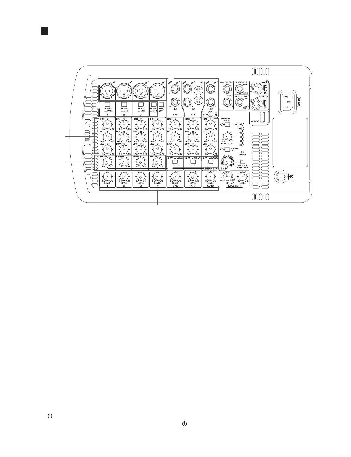
PANEL LAYOUT(パネルレイアウト)
STAGEPAS 600i
• Mixer panel
(ミキサーパネル)
/
4
)
0
1
6
2
*
-
q Mic/Line input jacks (channels 1-4)
w [MIC/LINE] switches (channels 1-4)
e [Hi-Z] switch (channel 4)
r [Line] (stereo) input jacks (channels 5/6, 7/8, 9/10)
t [MONITOR OUT] jacks
y [SUBWOOFER OUT] jack
u [REVERB FOOT] SW jack
i [SPEAKERS L/R] jacks
o [USB] connector
!0 [PHANTOM (CH1/2)] switch /LED
!1 [MONITOR OUT] control
!2 [Equalizer] controls (HIGH, MID, LOW)
!3 [REVERB] switch/LED
!4 [REVERB] TYPE/TIME control
!5 [REVERB] controls (channels 1-4)
!6 [ST/MONO] switches (channels 5/6, 7/8, 9/10)
!7 [LEVEL] meter
!8 POWER LED
!9 [FEEDBACK SUPPRESSOR] switch/LED
@0 [LEVEL] controls
@1 [MASTER EQ (equalizer)] control
@2 [MASTER LEVEL] control
@3 Vents
@4 [AC IN] jack
@5
(power) switch
qマイク / ライン入力端子(チャンネル1〜4)
w[MIC/LINE] スイッチ(チャンネル1〜4)
e[Hi-Z] スイッチ(チャンネル 4)
r
[ライン](ステレオ)入力端子(チャンネル5/6、7/8、9/10)
t[MONITOROUT] 端子
y[SUBWOOFEROUT] 端子
u[REVERBFOOTSW] 端子
i[SPEAKERSL/R] 端子
o[USB] 端子
!0[PHANTOM(CH1/2)] スイッチ /LED
!1[MONITOROUT] ツマミ
!2[イコライザー]ツマミ(HIGH、MID、LOW)
!3[REVERB] スイッチ /LED
!4[REVERBTYPE/TIME] ツマミ
!5[REVERB] ツマミ(チャンネル1〜4)
!6[ST/MONO] スイッチ(チャンネル 5/6、7/8、9/10)
!7[LEVEL] メーター
!8POWERLED
!9[FEEDBACKSUPPRESSOR
(フィードバックサプレッサー)] スイッチ /LED
@0[LEVEL] ツマミ
@1[MASTEREQ(イコライザー)] ツマミ
@2[MASTERLEVEL] ツマミ
@3通風孔
@4[ACIN] 端子
@5
(電源)スイッチ
5
STAGEPAS 600i
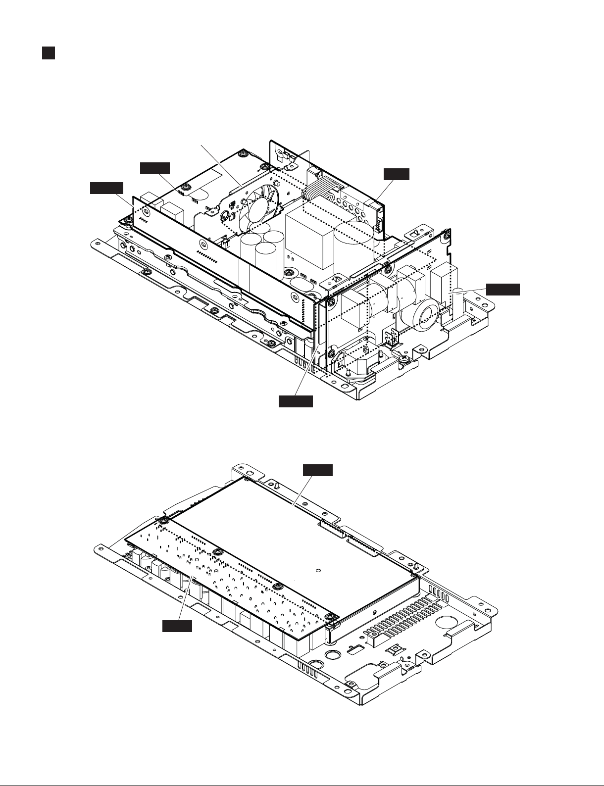
CIRCUIT BOARD LAYOUT(ユニットレイアウト)
● MIXER 600 ASSEMBLY(ミキサー 6 0 0 組 立 )
DC FAN
(DC ファン)
SUB63
AMPS
DSP
SUB61
SUB62
MIX62
MIX61
6
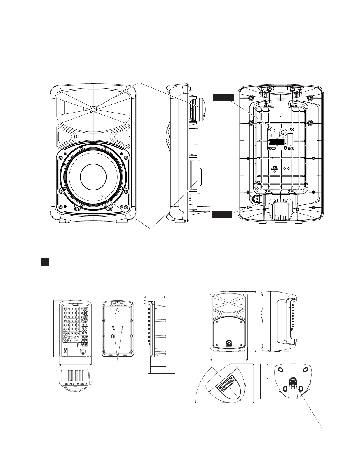
● SP 6 OVERALL ASSEMBLY(SP6総組立)
<Front view(正面)> <Right side view(右側面)> <Rear view(背面)>
LOUD SPEAKER (TWEETER)
(スピーカ(ツイーター))
NET61
STAGEPAS 600i
LOUD SPEAKER (WOOFER)
(スピーカ(ウーファー))
DIMENSIONS(寸法図)
● MIXER 600 ASSEMBLY(ミキサー 6 0 0 組 立 )
Unit: mm
348
197
Screw holes for the
Mic Stand Adapter
BMS-10A
(optional)
(マイクスタンド
アダプター
BMS-10A
(別売)用ネジ穴)
135
96
109
NET62
● SP 6 OVERALL ASSEMBLY(SP6総組立)
Unit: mm
545
335
2
50°
Pole diameter 34.8 - 35.2
* Use of the stand should refer to stand
manufacturer’s instructions.
(スタンド用穴
144
319
354
径34.8-35.2)
7
STAGEPAS 600i
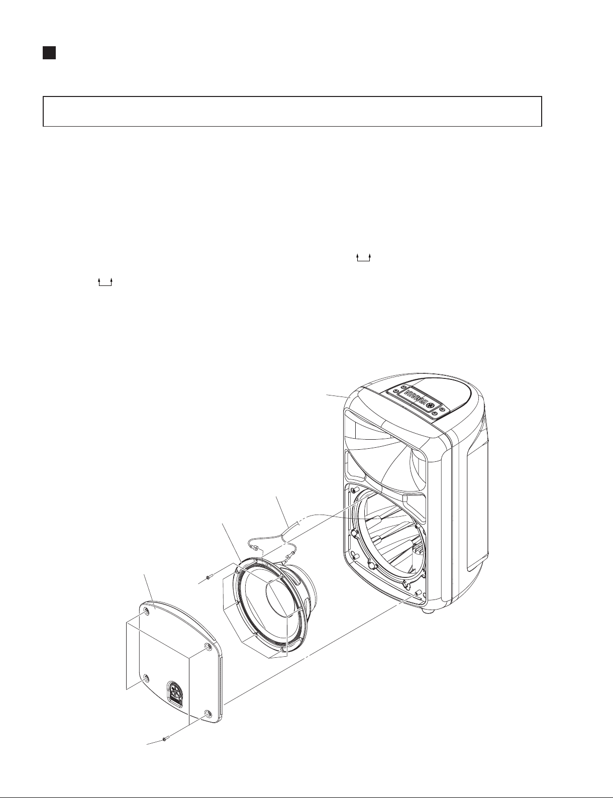
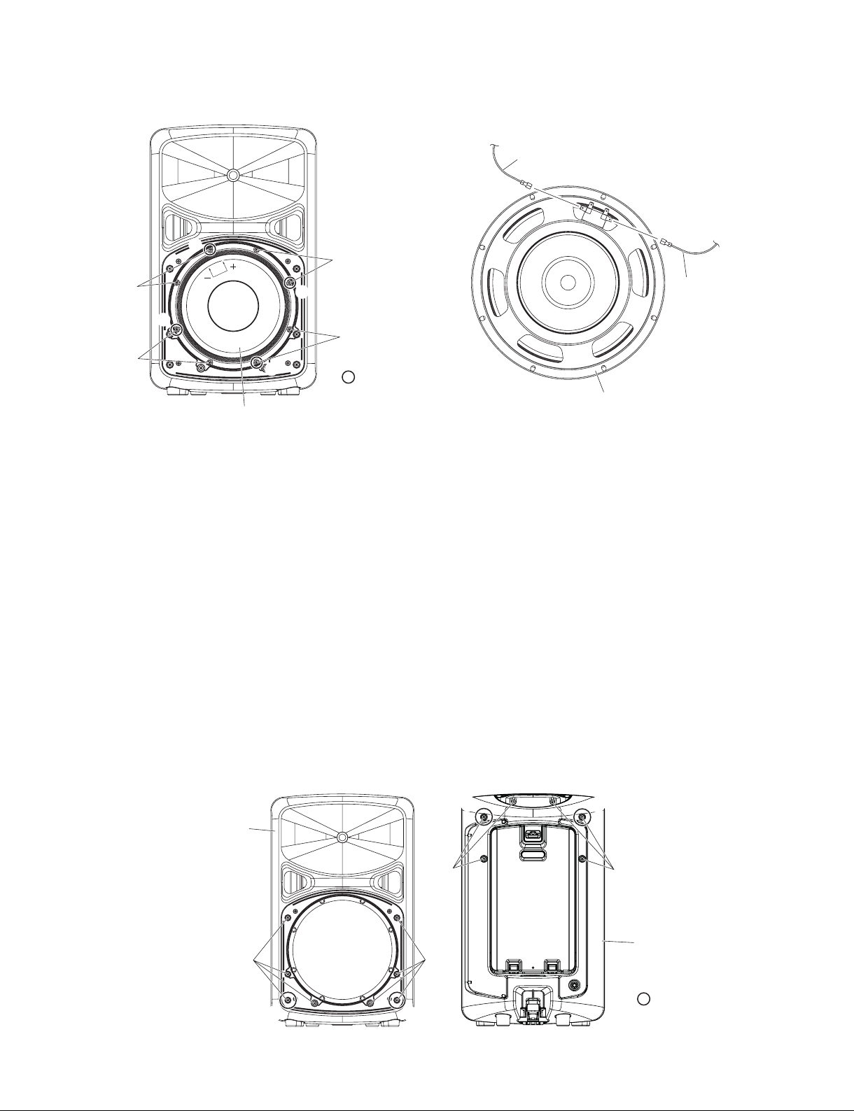
DISASSEMBLY PROCEDURE(分解手順)
A. Disassembly of STAGEPAS 600i
* When you remove binding ties and such, always
install as before removal.
A-1. Grille 6 Assembly (Time required: About 1 minute)
A-1-1 Remove the four (4) screws marked [360]. The grille 6
assembly can then be removed. (Fig. A-1)
A-2.
Loud Speaker (Woofer) (Time required: About 2 minutes)
A-2-1 Remove the grille 6 assembly. (See procedure A-1.)
A-2-2 Remove the eight (8) screws marked [340]. The loud
speaker (woofer) can then be removed.
(Fig. A-1, Fig. A-2)
* When installing the speaker (woofer), first match
the position of the terminal to the direction shown
by the
priority screws in order as shown in Fig. A-2.
A-2-3 Remove the NWINOUT6 connector assembly (red/
black) attached to the speaker (woofer) terminal.
(Fig. A-1, Fig. A-3)
* The speaker (woofer) is heavy. Be careful not to
drop it.
* When you remove the NWINOUT6 connector
assembly, be careful not to tear the cushion.
mark and then tighten the four (4)
BAFFLE 6 ASSEMBLY
(バッフル6組立)
A.STAGEPAS600i の分解
※ インシュロックタイなどを外したときは必ず外す前と
同じように取付けてください。
A-1. グリル 6 組立(所要時間:約1分)
A-1-1 [360] のネジ 4 本を外して、グリル 6 組立を外しま
す(図 A-1)
A-2. スピーカ(ウーファー)
A-2-1 グリル 6 組立を外します。(A-1 項参照)
A-2-2 [340] のネジ 8 本を外して、スピーカ(ウーファー)
を外します(図 A-1、図 A-2)
※ スピーカ(ウーファー)を取り付けるときは、端子の位
置を
示す順番で先に締めてください。(図 A-2)
印の方向に合わせてから、優先ネジ 4 本を図に
A-2-3 スピーカ(ウーファー)端子に取り付けられてい
る NWINOUT 束線 6(赤/黒)を外します。
(図 A-1、図 A-3)
※ スピーカ(ウーファー)は重量がありますので、落下さ
せない様に注意してください。
※ NWINOUT 束線 6 を外す際は、クッションを破らない
ように注意してください。
(所要時間:約2分)
NWINOUT6 CONNECTOR ASSEMBLY
LOUD SPEAKER(スピーカ)
(WOOFER)
GRILLE 6 ASSEMBLY
(グリル6組立)
[340]
[360]
(RED/BLACK)
(NWINOUT束線6(赤/黒))
Fig. A-1
(図A-1)
8
STAGEPAS 600i
• Front view(前面)
/
[340]
[340]
0
)
[340]
[340]
LOUD SPEAKER(スピーカ)
(WOOFER)
Fig. A-2
4
(図A-2)
: PRIORITY SCREW
(優 先ネジ)
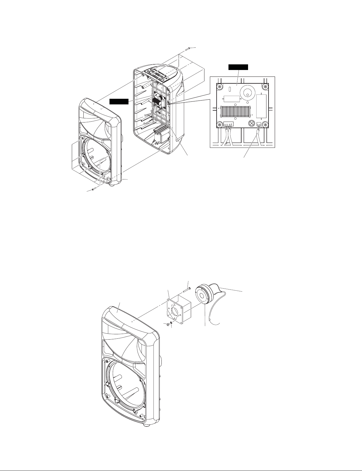
A-3. Baffle 6 Assembly (Time required: About 5 minutes)
A-3-1 Remove the grille 6 assembly. (See procedure A-1.)
Remove the loud speaker (woofer). (See procedure A-2.)
A-3-2
* Remove the loud speaker (woofer) to avoid
damaging the connector assembly.
A-3-3 Remove the eight (8) screws marked [320] and six (6)
screws marked [370]. The baffl e 6 assembly can then
be removed. (Fig. A-4, Fig. A-5)
*
When installing the baffle 6 assembly, first tighten the
two (2) priority screws each, as shown in Fig. A-4.
(Fig. A-4)
A-3-4 Disconnect the connectors of the HFSPOUT connector
assembly (yellow/blue) from the NET61 circuit board.
(Fig. A-5)
* Be careful not to open the baffle 6 assembly too far
and not to damage the HFSPOUT connector assembly
(yellow/blue).
• Rear view(背面)
NWINOUT6 CONNECTOR
ASSEMBLY (RED +)
(NWINOUT束線6(赤+))
NWINOUT6 CONNECTOR
ASSEMBLY (BLACK -)
(NWINOUT束線6(黒−))
LOUD SPEAKER(スピーカ)
(WOOFER)
Fig. A-3
(図A-3)
A-3. バッフル 6 組立(所要時間:約 5 分)
A-3-1 グリル 6 組立を外します。(A-1 項参照)
A-3-2 スピーカ(ウーファー)を外します。(A-2 項参照)
※ 束線を傷めないようにするために、スピーカ(ウー
ファー)を外します。
A-3-3 [320] のネジ 8 本と [370] のネジ 6 本を外して、バッ
フル 6 組立を外します。(図 A-4、図 A-5)
※ バッフル 6 組立を取り付けるときは、図に示す優先ネジ
各 2 本を先に締めてください。(図 A-4)
A-3-4 NET61 シートからHFSPOUT 束 線(黄/青)、
のコネクターを外します。(図 A-5)
※ バッフル 6 組立を開きすぎて、HFSPOUT 束線(黄/青)
を傷めないように注意してください。
BAFFLE 6 ASSEMBLY
(バッフル6組立)
[320]
• Front view(前面)
/
[370]
[320]
/
Fig. A-4
• Rear view(背面)
&
(図A-4)
&
[370]
CABINET 6 ASSEMBLY
(キャビネット6組立)
: PRIORITY SCREW
(優 先ネジ)
9
STAGEPAS 600i
[320]
NET62
BAFFLE 6 ASSEMBLY
(バッフル6組立)
Fig. A-5
(図A-5)
[370]
NET62
HFSPOUT CONNECTOR
ASSEMBLY (YELLOW/BLUE)
(HFSPOUT束線(黄/青))
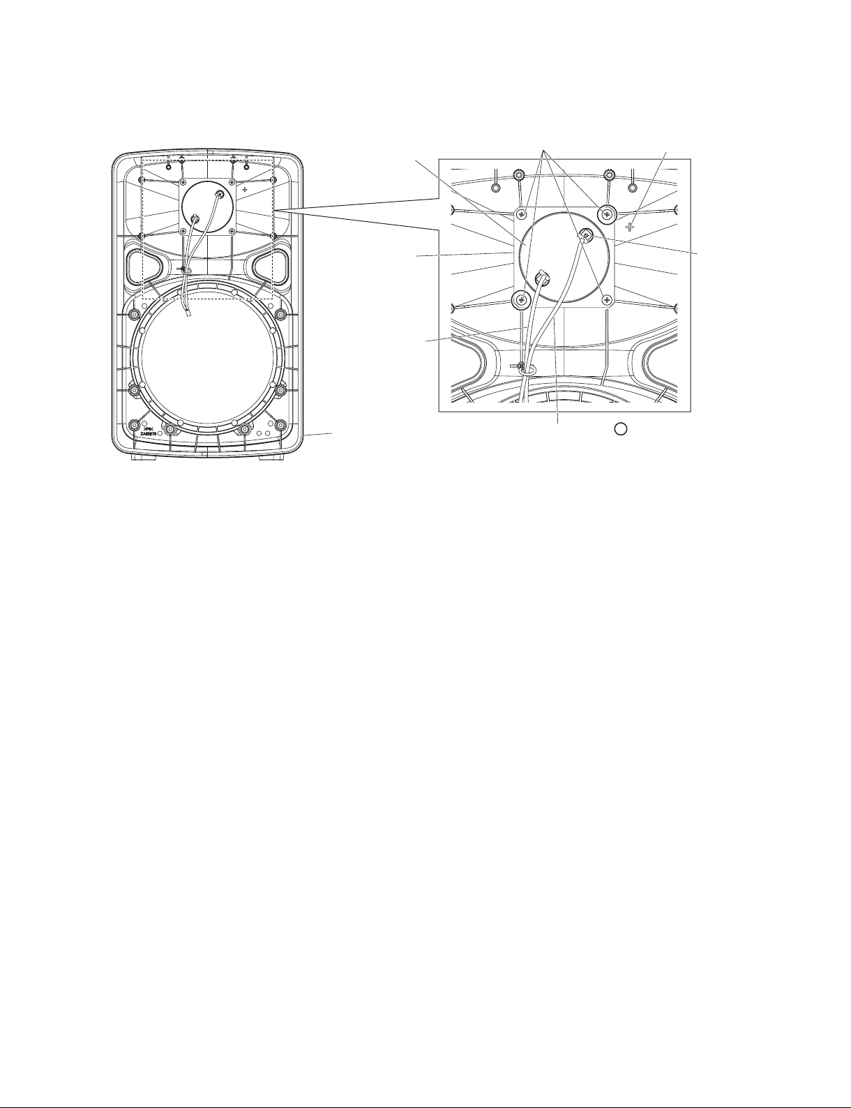
A-4.
Speaker (Tweeter) (Time required: About 7 minutes)
A-4-1 Remove the grille 6 assembly. (See procedure A-1.)
A-4-2 Remove the loud speaker (woofer). (See procedure A-2.)
A-4-3 Remove the baffl e 6 assembly. (See procedure A-3.)
A-4-4 Remove the HFSPOUT connector assembly (yellow/
blue) attached to the speaker (tweeter) terminal.
(Fig. A-6, Fig. A-7)
TW PLATE
BAFFLE 4 ASSEMBLY
(バッフル4組立)
(TWプレート)
[40]
A-4. スピーカ(ツイーター)(所要時間:約 7 分)
A-4-1 グリル 6 組立を外します。(A-1 項参照)
A-4-2 スピーカ(ウーファー)を外します。(A-2 項参照)
A-4-3 バッフル 6 組立を外します。(A-3項参照)
A-4-4 スピーカ(ツイーター)端子に取り付けられてい
る HFSPOUT 束線(黄/青)を外します。
(図 A-6、図 A-7)
[60]
HFSPOUT CONNECTOR
ASSEMBLY (YELLOW/BLUE)
(HFSPOUT束線(黄/青))
LOUD SPEAKER(スピーカ)
[50]
(TWEETER)
10
Fig. A-6
(図A-6)
STAGEPAS 600i
• Rear view(背面)
LOUD SPEAKER(スピーカ)
(TWEETER)
TW PLATE
(TWプレート)
HFSPOUT CONNECTOR
ASSEMBLY (BLUE)
(HFSPOUT束線(青))
BAFFLE 6 ASSEMBLY
(バッフル6組立)
Fig. A-7
(図A-7)
[60]
/
HFSPOUT CONNECTOR
ASSEMBLY (YELLOW)
(HFSPOUT束線(黄))
“+”MARKING
(+マーク )
/
RED MARKING
(赤色マーク)
: PRIORITY SCREW
(優 先ネジ)
A-4-5 Remove the four (4) screws marked [60]. The TW plate
can then be removed together with the speaker (tweeter).
(Fig. A-6, Fig. A-7)
* When installing the TW plate, first match the red
marking on the speaker (tweeter) to the "+" marking
on the baffle 6 assembly and then tighten the two (2)
priority screws. (Fig. A-7)
A-4-6 Remove the four (4) screws marked [40] and four (4)
washers o. tooth marked [50]. The speaker (tweeter) can
then be removed from the TW plate. (Fig. A-6)
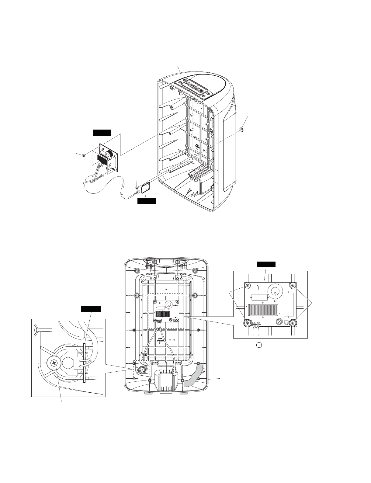
A-5. NET61 Circuit Board (Time required: About 7 minutes)
A-5-1 Remove the grille 6 assembly. (See procedure A-1.)
A-5-2 Remove the loud speaker (woofer). (See procedure A-2.)
A-5-3 Remove the baffl e 6 assembly. (See procedure A-3.)
A-5-4 Remove the four (4) screws marked [130]. The NET61
circuit board can then be removed. (Fig. A-8, Fig. A-9)
* When installing the NET61 circuit board, first tighten
the two (2) priority screws as shown in Fig. A-9.
A-6.
NET62 Circuit Board (Time required: About 7 minutes)
A-6-1 Remove the grille 6 assembly. (See procedure A-1.)
A-6-2 Remove the loud speaker (woofer). (See procedure A-2.)
A-6-3 Remove the baffl e 6 assembly. (See procedure A-3.)
A-6-4 Remove the screw marked [160] and plastic nut. The
NET62 circuit board can then be removed.
(Fig. A-8, Fig. A-9)
A-4-5 [60] のネジ 4 本を外して、スピーカ(ツイーター)
と共に TW プレートを外します。
(図 A-6、図 A-7)
※ TW プレートを取り付けるときは、スピーカ(ツイー
ター)の赤色マークをバッフル 6 組立の"+"マークの
方向に合わせてから、優先ネジ 2 本を先に締めてくださ
い。(図 A-7)
A-4-6 [40] のネジ 4 本と [50] の歯付座金外歯 4 個を外し
て、TW プレートからスピーカ(ツイーター)を
外します。(図 A-6)
A-5. NET61 シート
(所要時間:約 7 分)
A-5-1 グリル 6 組立を外します。(A-1 項参照)
A-5-2 スピーカ(ウーファー)を外します。(A-2 項参照)
A-5-3 バッフル 6 組立を外します。(A-3項参照)
A-5-4 [130]のネジ 4本を外して、NET61 シートを外し
ます。(図 A-8、図 A-9)
※ NET61 シートを取り付けるときは、図に示す優先ネジ
2 本を先に締めてください。(図 A-9)
A-6. NET62 シート(所要時間:約 7 分)
A-6-1 グリル 6 組立を外します。(A-1 項参照)
A-6-2 スピーカ(ウーファー)を外します。(A-2 項参照)
A-6-3 バッフル 6 組立を外します。(A-3項参照)
A-6-4 [160] のネジ 1 本とプラスチックナットを外して、
NET62 シートを外します。(図 A-8、図 A-9)
11
STAGEPAS 600i
CABINET 6 ASSEMBLY
(キャビネット6組立)
Plastic nut
(プラスチックナット)
NET61
[130]
[160]
NET62
NET62
Fig. A-8
(図A-8)
[130]
/
NET61
[130]
4
: PRIORITY SCREW
(優 先ネジ)
12
[160]
Fig. A-9
CABINET 6 ASSEMBLY
(キャビネット6組立)
(図A-9)
STAGEPAS 600i
A-7.
Mixer 600 Assembly, ACCS Lid 6 Assembly
(Time required: About 1 minute)
Mixer 600 Assembly
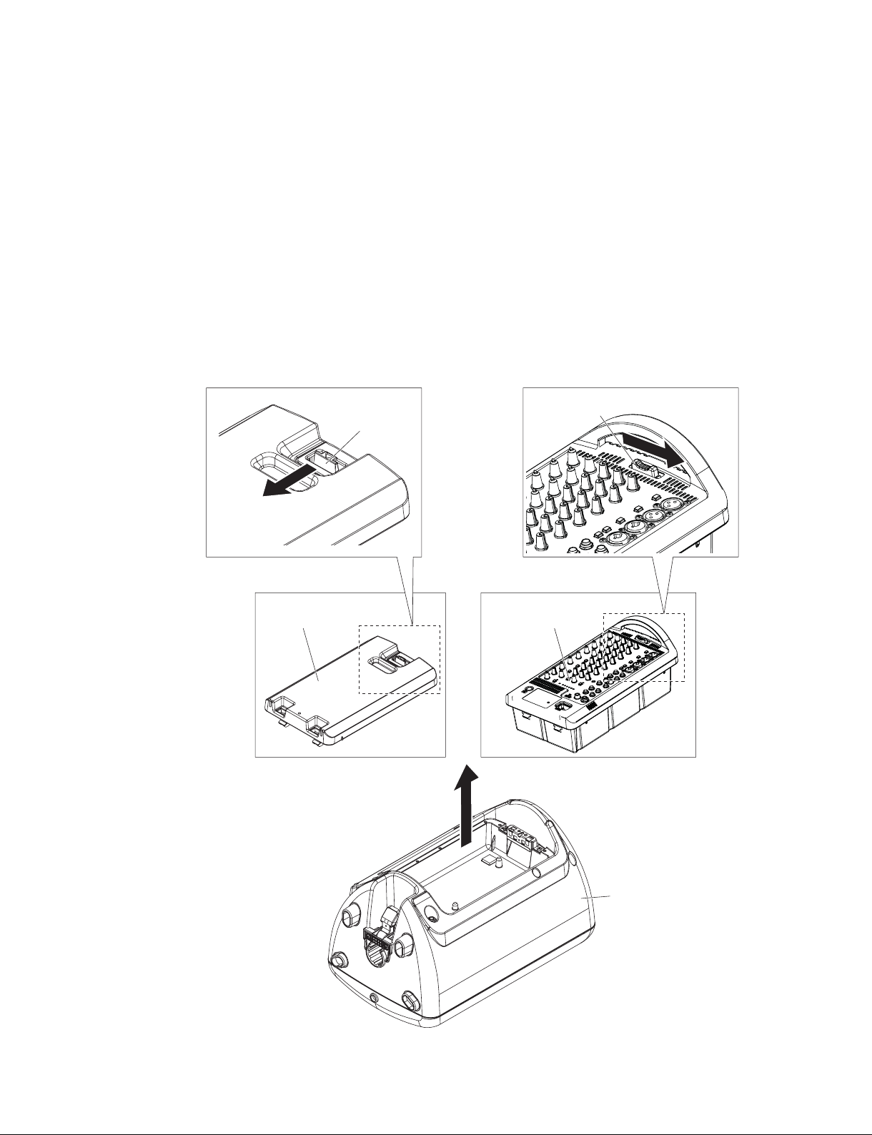
A-7-1
A-7-1-1
Slide the slide knob in the direction of the arrow in the
fi gure, while pulling the mixer 600 assembly forward
to remove it. (Fig.A-10)
ACCS Lid 6 Assembly
A-7-2
A-7-2-1
Press the knob in the direction of the arrow in the
fi gure, while pulling the ACCS lid 6 assembly forward
to remove it. (Fig. A-10)
For about disassembly of mixer 600 assembly, refer to
14 p a ge.
KNOB
(ノブ)
A-7. ミキサー 600 組立、ACCS 蓋 6 組立の外し方
(所要時間:約 1 分)
A-7-1 ミキサー 600 組立
A-7-1-1
ノブスライドを図の矢印の方向へずらしながら手
前に引いてミキサー 600 組立を外します。
(図 A-10)
A-7-2
ACCS蓋6組立
A-7-2-1
図のノブを矢印の方向へ押しながら手前に引いて
ACCS 蓋 6 組立を外します。(図 A-10)
ミキサー 600 組立の分解手順は、14 ページを参
照してください。
SLIDE KNOB
(ノブスライド)
ACCS LID 6 ASSEMBLY
(ACCS蓋6組立)
MIXER 600 ASSEMBLY
(ミキサー600組立)
or
CABINET 6 ASSEMBLY
(キャビネット6組立)
Fig. A-10
(図A-10)
13
STAGEPAS 600i
B. Disassembly of mixer 600 assembly
* Before disassembly, remove the mixer 600 assembly or
ACCS lid 6 assembly in advance. (See procedure A-7.)
* When you remove binding ties and such, always install
as before removal.
* To inspect and check the electrical components of the
mixer 600 assembly, see “How to use the EXT JIG circuit
board” (page 71) for the disassembling procedure
to disassemble the mixer 600 assembly and connect
CN505 of the DSP circuit board and CN511 of the AMPS
circuit board by the EXT JIG circuit board.
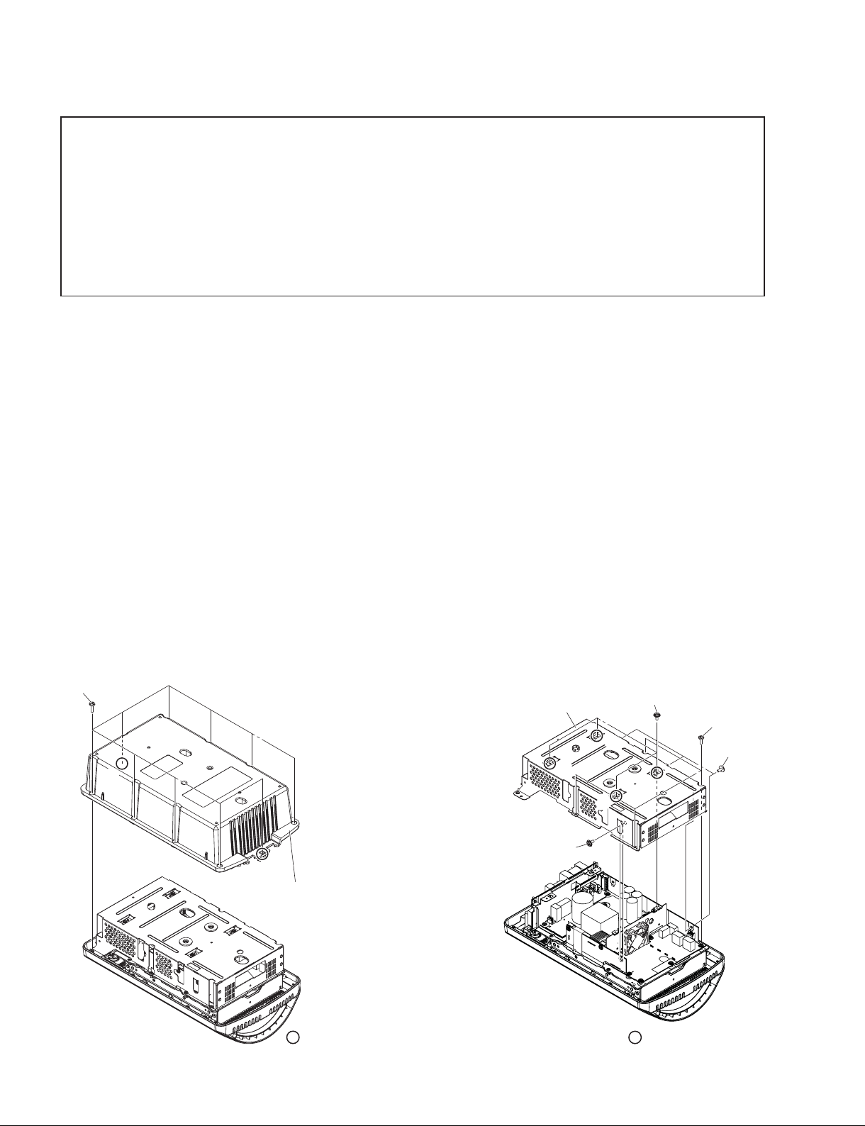
B-1. Bottom Cover 6 Assembly
(Time required: About 2 minutes)
B-1-1 Remove the ten (10) screws marked [530]. The bottom
cover 6 assembly can then be removed. (Fig. B-1)
* When installing the bottom cover 6 assembly, first
tighten the two (2) priority screws in order as shown
in Fig. B-1.
B-2. Shield Mix 6 Assembly
(Time required: About 4 minutes)
B-2-1 Remove the bottom cover 6 assembly.
(See procedure B-1.)
B-2-2 Remove the four (4) screws marked [440] and eight (8)
screws marked [450]. The shield mix 6 assembly can
then be removed. (Fig. B-2)
* When installing the shield mix 6 assembly, first
tighten the screws marked [450] and then tighten
the screws marked [440]. (Fig. B-2)
* For the screws marked [440], first tighten the four (4)
priority screws in order as shown in Fig. B-2.
(Fig. B-2)
[530]
4
B.ミキサー 600 組立の分解
※ 分解の前に、あらかじめミキサー 600 組立または
ACCS 蓋 6 組立を外しておきます。(A-7 項参照)
※ インシュロックタイなどを外したときは必ず外す前と
同じように取付けてください。
※ ミキサー 600 組立の電気部品のチェックは、EXTJIG
シートの使用法(71 ページ)を参考に、分解手順に従っ
て、ミキサー 600組立を分解して EXT JIG シートで
DSP シートの CN505 と AMPS シートの CN511 を接
続して点検・チェックしてください。
B-1. 下カバー 6 組立(所要時間:約2分)
B-1-1 [530] のネジ 10 本を外して、下カバー 6 組立を外
します(図 B-1)
※ 下カバー 6 組立を取り付けるときには、優先ネジ 2 本を
図に示す順で先に締めてください。(図 B-1)
B-2. シールド MIX6 組立(所要時間:約4分)
B-2-1 下カバー 6 組立を外します。(B-1 項参照)
B-2-2 [440] のネジ 4 本と [450] のネジ 8 本を外して、シー
ルド MIX6 組立を外します(図 B-2)
※ シールド MIX6 組立を取り付けるときには、先に [450]
のネジを締めてから [440] のネジを締めてください。
[440] のネジは、優先ネジ 4 本を図に示す順で先に締め
てください。(図 B-2)
0
[450]
[440]
[450]
SHIELD MIX 6 ASSEMBLY
(シールドMIX6組立)
)
4
/
14
/
BOTTOM COVER 6 ASSEMBLY
(下カバー6組立)
: PRIORITY SCREW
(優 先ネジ)
Fig. B-1
(図B-1)
[450]
Fig. B-2
: PRIORITY SCREW
(優 先ネジ)
(図B-2)

STAGEPAS 600i
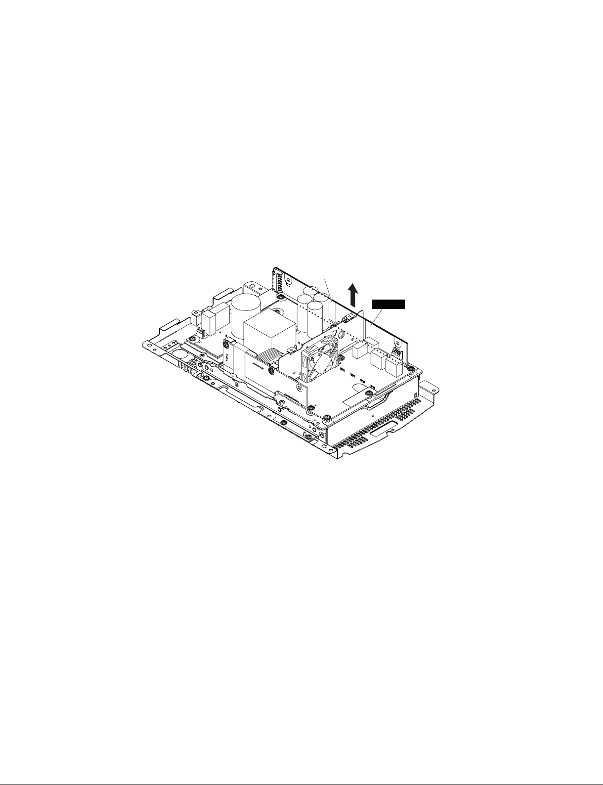
B-3. DSP Circuit Board
(Time required: About 5 minutes)
B-3-1 Remove the bottom cover 6 assembly.
(See procedure B-1.)
B-3-2 Remove the shield mix 6 assembly.
(See procedure B-2.)
B-3-3 Remove the two (2) screws marked [410].
Remove the DSP circuit board by pulling it in the
direction of the arrow in Fig. B-3.(Fig. B-3)
* When removing the DSP circuit board, be sure to
remove CN505 of the DSP circuit board and CN511
of the AMPS circuit board.
As shown in Fig. B-3, use either a flat-blade
screwdriver or steel rule to open between the circuit
boards. (Fig. B-3)
* When removing the DSP circuit board, be sure that
the capacitors C435 and C439 do not contact the
PNL shield 6 assembly. If the DSP circuit board
is removed without care, the DSP circuit board
contacts the PNL shield 6 assembly, resulting in
possible malfunction.
B-3-4 Remove the two (2) nylon rivets marked [412]. The
insulation sheet DSP can then be removed. (Fig. B-3)
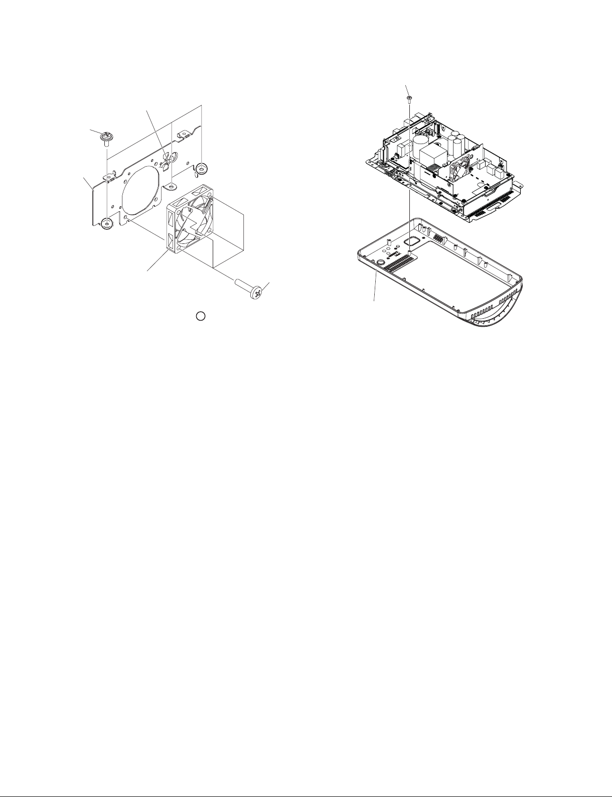
B-4. DC Fan
(Time required: About 7 minutes)
B-4-1 Remove the bottom cover 6 assembly.
(See procedure B-1.)
B-4-2 Remove the shield mix 6 assembly.
(See procedure B-2.)
B-4-3 Remove the three (3) screws marked [380]. The angle
fan 6 can then be removed together with the DC fan.
(Fig. B-3, Fig. B-4)
* When installing the angle fan 6, first tighten the two
(2) priority screws in order as shown in Fig. B-4.
B-4-4 Remove the four (4) screws marked [360]. The DC fan
can then be removed. (Fig. B-4)
* Be sure to remove binding tie A. Install as before
binding tie A was removed. (Fig. B- 4)
B-3. DSP シート(所要時間:約5分)
B-3-1 下カバー 6 組立を外します。(B-1 項参照)
B-3-2 シールド MIX6 組立を外します。(B-2 項参照)
B-3-3 [410] のネジ 2 本を外して、DSP シートを図 B-3
の矢印の方向へ引き抜いて外します。(図 B-3)
※ DSP シートを外すときは、先に DSP シートの CN505
と AMPS シートの CN511 を外します。
マイナスドライバーか金尺で、図 B-3 のように基板間を
こじあけるようにして浮かせます。(図 B-3)
※ DSP シートを外すときは、コンデンサ C435 と C439
が PNL シールド 6 組立に当たらないように注意してく
ださい。無造作に引き抜くと、PNL シールド 6 組立に
DSP シートがあたって、破損する恐れがあります。
B-3-4 [412] のプラスチックリベット 2 個を外して、絶縁
シート DSP を外します。(図 B-3)
B-4. DC ファン
(所要時間:約7分)
B-4-1 下カバー 6 を外します。(B-1 項参照)
B-4-2 シールド MIX6 組立を外します。(B-2 項参照)
B-4-3 [380] の ネ ジ 3 本を外して、DC ファンと共に
FAN 金具 6 を外します。(図 B-3、図 B-4)
※ FAN 金具 6 を取り付けるときには、優先ネジ 2 本を図
に示す順で先に締めてください。(図 B-4)
B-4-4 [360] のネジ 4 本を外して、DC ファンを外します。
(図 B-4)
※ インシュロックタイ A を必ず外してください。
取付けるときには、インシュロックタイ A を取り外す前
と同じように取り付けてください。(図 B-4)
INSULATION SHEET DSP
(絶縁シートDSP)
PNL SHIELD 6 ASSEMBLY
(PNLシールド6組立)
[412]
[380]
DC FAN
(DCファン)
AMPS
DSP
[410]
ANGLE FAN 6
(FAN金具6)
B-5. Top Cover 6
(Time required: About 4 minutes)
B-5-1 Remove the bottom cover 6 assembly.
(See procedure B-1.)
B-5-2 Remove the shield mix 6 assembly.
(See procedure B-2.)
B-5-3 Remove the screw marked [210]. The top cover 6 can
then be removed. (Fig. B-5)
Fig. B-3
AMPS
: CN505
DSP
DSP
: CN511
AMPS
Flat-blade screwdriver or Steel rule
(マイナスドライバーまたは金尺)
(図B-3)
B-5. トップカバー 6 塗装品
(所要時間:約4分)
B-5-1 下カバー 6 組立を外します。(B-1 項参照)
B-5-2 シールド MIX6 組立を外します。(B-2 項参照)
B-5-3 [210] のネジ 1 本を外して、トップカバー 6 塗装品
を外します。(図 B-5)
15
STAGEPAS 600i
[380]
ANGLE FAN 6
(FAN金具6)
[210]
BINDING TIE A
(インシュロックタイA)
/
4
DC FAN
(DCファン)
Fig. B-4
: PRIORITY SCREW
(優 先ネジ)
(図B-4)
[360]
B-6. SUB61 Circuit Board, SUB62 Circuit Board
(Time required: About 7 minutes)
B-6-1 Remove the bottom cover 6 assembly.
(See procedure B-1.)
B-6-2 Remove the shield mix 6 assembly.
B-6-3 Remove the top cover 6.
B-6-4
SUB61 Circuit Board
B-6-4-1
Remove the screw marked [110] and four (4) screws
(See procedure B-5.)
(See procedure B-2.)
marked [90]. The ACIN shield 6 can then be removed
together with the SUB61 circuit board. (Fig. B-6)
* When installing the ACIN shield 6, first tighten the
two (2) priority screws as shown in Fig. B- 6.
B-6-4-2
Remove the power knob, two (2) screws marked [50]
and four (4) screws marked [70]. The SUB61 circuit
board can then be removed. (Fig. B-6)
* Be sure to remove binding tie B and remove binding
tie C. Install as before binding tie B and binding tie
C was removed. (Fig. B-6)
* When installing the SUB61 circuit board, first tighten
the screws marked [50] and then the screws marked
[70].
First tighten their priority screws in order as shown
in Fig. B-6. (Fig. B-6)
B-6-4-3
Straightenthetwoclawsoftheinletangleand
removetheinletanglefromthe
board
.(Fig.B-6)
* The power knob and the inlet angle are not parts of
the SUB61 circuit board. When replacing the SUB61
circuit board, remove the power knob and the inlet
angle from the SUB61 circuit board and install them
to the new circuit board. (Fig. B- 6)
SUB61 circuit
TOP COVER 6
(トップカバー6塗装品)
Fig. B-5
(図B-5)
B-6. SUB61 シート、SUB62 シート(所要時間:約7分)
B-6-1 下カバー 6 組立を外します。(B-1 項参照)
B-6-2 シールド MIX6 組立を外します。(B-2 項参照)
B-6-3 トップカバー 6 塗装品を外します。(B-5 項参照)
B-6-4 SUB61 シート
B-6-4-1
[110] の ネ ジ 1 本 と [90] の ネ ジ 4 本を外して、
SUB61 シートと共に ACIN シールド 6 を外しま
す。(図 B-6)
※ ACIN シールド 6 を取り付けるときには、優先ネジ 2 本
を図に示す順で先に締めてください。(図 B-6)
B-6-4-2
パワーノブ 1 個と [50] のネジ 2 本と [70] のネジ 4
本を外して、SUB61 シートを外します。(図 B-6)
※ インシュロックタイ B とインシュロックタイ C を必ず
外してください。
取付けるときには、インシュロックタイ B とインシュ
ロックタイ C を取り外す前と同じように取り付けてく
ださい。(図 B-6)
※ SUB61 シートを取り付けるときには、先に [50] のネジ
を締めてから [70] のネジを締めてください。
このとき、それぞれの優先ネジを図に示す順で先に締め
てください。(図 B-6)
B-6-4-3
インレット金具のツメ 2 箇所をまっすぐに伸ばし
て、SUB61 シートからインレット金具を外します。
(図 B-6)
※ パワーノブとインレット金具は SUB61 シートの構成部
品ではありません。SUB61 シートを交換する際には、
SUB61 シートからパワーノブとインレット金具を取り
外して、新しいシートに取り付けてください。(図 B-6)
16
STAGEPAS 600i
INLET ANGLE
(インレット金具)
[110]
MIXER PANEL 6
ASSEMBLY
(MIXパネル6組立)
: PRIORITY SCREW
(優先ネジ)
[70]
/
[90]
SUB61
&
4
ACIN SHIELD 6
(ACINシールド6)
[50]
POWER KNOB
(パワーノブ)
(プラスチックナット)
[100]
CUSHION A
(クッションA)
SUB62
Plastic nut
*
Raise the inlet angle claws
SUB61
(INLET ANGLE(インレット金具))
A view
Crow(ツメ)
(A視図)
SUB61
ACIN SHIELD 6
(ACINシールド6)
to be straight in the directions
of the arrows.
(※インレット金具のツメを
矢印の方向にまっすぐに
なるように起こしてくだ
さい。)
BINDING TIE C(インシュロックタイC)
BINDING TIE B(インシュロックタイB)
A
AMPS
Fig.B-6
B-6-5 SUB62 Circuit Board
B-6-5-1
Remove the SUB61 circuit board.
(See procedure B-6-4.)
B-6-5-2 Remove the two (2) plastic nuts and screw marked [100].
The SUB62 circuit board can then be removed. (Fig. B-6)
* The cushion A are not parts of the SUB62 circuit
board. When replacing the SUB62 circuit board,
remove the cushion A from the SUB62 circuit board
and install them to the new circuit board. (Fig. B-6)
(図B-6)
B-6-5 SUB62 シート
B-6-5-1
SUB61 シートを外します。(B-6-4 項参照)
B-6-5-2
プラスチックナット 2 個と [100] のネジ 1 本を外
して、SUB62 シートを外します。(図 B-6)
※ クッション A は SUB62 シートの構成部品ではありませ
ん。SUB62 シートを交換する際には取り外して、新し
いシートに取り付けてください。(図 B-6)
17
STAGEPAS 600i
B-7.
SUB63 Circuit Board (Time required: About 7 minutes)
B-7-1 Remove the bottom cover 6 assembly.
(See procedure B-1.)
B-7-2 Remove the shield mix 6 assembly.
B-7-3 Remove the top cover 6.
(See procedure B-5.)
B-7-4 Remove the SUB61 circuit board and SUB62 circuit
(See procedure B-6.)
board.
B-7-5 Pull out the SUB63 circuit board in the direction of the
arrow in the fi gure. (Fig. B-7)
* The cushion B are not parts of the SUB63 circuit
board. When replacing the SUB63 circuit board,
remove the cushion B from the SUB63 circuit board
and install them to the new circuit board. (Fig. B-7)
(See procedure B-2.)
B-7. SUB63 シート(所要時間:約7分)
B-7-1 下カバー 6 組立を外します。(B-1 項参照)
B-7-2 シールド MIX6 組立を外します。(B-2 項参照)
B-7-3 トップカバー 6 塗装品を外します。(B-5 項参照)
B-7-4 SUB61 シートと SUB62 シートを外します。
(B-6 項参照)
B-7-5 SUB63 シートを図の矢印の方向へ引き抜きます。
(図 B-7)
※ クッション B は SUB63 シートの構成部品ではありませ
ん。SUB63 シートを交換する際には取り外して、新し
いシートに取り付けてください。(図 B-7)
CUSHION B
(クッションB)
SUB63
B-8.
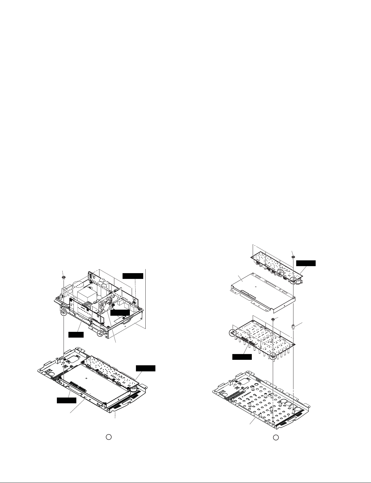
AMPS Circuit Board (Time required: About 10 minutes)
B-8-1 Remove the bottom cover 6 assembly.
(See procedure B-1.)
B-8-2 Remove the shield mix 6 assembly.
B-8-3 Remove the DSP circuit board.
(See procedure B-2.)
(See procedure B-3.)
B-8-4 Remove the DC fan and the angle fan 6.
(See procedure B-4.)
B-8-5 Remove the top cover 6.
(See procedure B-5.)
B-8-6 Remove the SUB61 circuit board and SUB62 circuit
board. (See procedure B-6.)
B-8-7 Remove the SUB63 circuit board. (See procedure B-7.)
B-8-8 Remove the twelve (12) screws marked [310] and nylon
rivet marked [300]. The AMPS circuit board can then
be removed. (Fig. B-8)
* When installing the AMPS circuit board, first tighten
the two (2) priority screws as shown in Fig. B-8.
18
Fig.B-7
(図B-7)
B-8. AMPS シート(所要時間:約10分)
B-8-1 下カバー 6 組立を外します。(B-1 項参照)
B-8-2 シールド MIX6 組立を外します。(B-2 項参照)
B-8-3 DSP シートを外します。(B-3 項参照)
B-8-4 DC ファンと FAN 金具 6 を外します。(B-4 項参照)
B-8-5 トップカバー 6 塗装品を外します。(B-5 項参照)
B-8-6 SUB61 シートと SUB62 シートを外します。
(B-6 項参照)
B-8-7 SUB63 シートを外します。(B-7 項参照)
B-8-8 [310] のネジ 12 本と [300] のプラスチックリベッ
ト 1 個を外して、AMPS シートを外します。
(図 B-8)
※ AMPS シートを取り付けるときには、優先ネジ 2 本を
図に示す順で先に締めてください。(図 B-8))
W
[310]
STAGEPAS 600i
4
AMPS
/
[300]
HEATSINK AMPS6 ASSEMBLY
(HSAMPS6組立)
PNL SHIELD 6 ASSEMBLY
(PNLシールド6組立)
MIXER PANEL 6 ASSEMBLY
(MIXパネル6組立)
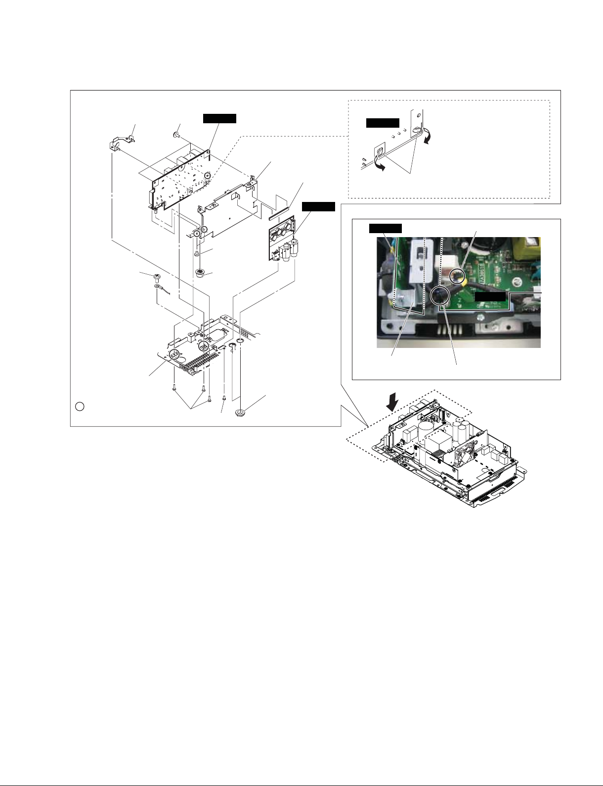
B-9. MIX61 Circuit Board, MIX62 Circuit Board
(Time required: About 15 minutes)
B-9-1
Remove the bottom cover 6 assembly.
(See procedure B-1.)
B-9-2
Remove the shield mix 6 assembly.
B-9-3
Remove the top cover 6.
B-9-4
Remove the SUB61 circuit board and SUB62 circuit
(See procedure B-5.)
(See procedure B-2.)
board. (See procedure B-6.)
B-9-5 Remove the six (6) screws marked [180]. The PNL
shield 6 assembly can then be removed together with the
AMPS circuit board, DSP circuit board, SUB63 circuit
board and DC fan. (Fig. B-9)
*
When installing the PNL shield 6 assembly, first tighten
the two (2) priority screws as shown in Fig. B-9.
Fig.B-8
INSULATION SHEET PS 6
(絶縁シートPS6)
: PRIORITY SCRE
(優 先ネジ)
(図B-8)
B-9. MIX61 シート、MIX62 シート(所要時間:約15分)
B-9-1 下カバー 6 組立を外します。(B-1 項参照)
B-9-2 シールド MIX6 組立を外します。(B-2 項参照)
B-9-3 トップカバー 6 塗装品を外します。(B-5 項参照)
B-9-4 SUB61 シートと SUB62 シートを外します。
(B-6 項参照)
B-9-5 [180] のネジ6 本を外して、AMPS シート、DSP シー
ト、SUB63 シート、DC ファンと共に PNL シー
B-9
ルド 6 組立を外します。(図
※ PNL シールド 6 組立を取り付けるときには、優先ネジ 2
本を図に示す順で先に締めてください。(図 B-9)
)
19
STAGEPAS 600i
W
B-9-6 MIX61 Circuit Board
B-9-6-1
Remove the four (4) screws marked [160], nine (9)
screws marked [540], ten (10) nuts marked [A] and ten
(10) washers marked [B]. The MIX61 circuit board can
then be removed. (Fig. B-10, Fig. B-11)
* The below parts are not components of the MIX61
circuit board. When replacing the MIX61 circuit board,
remove the below parts from the MIX61 circuit board
and install them to the new circuit board. (Fig. B-11)
[150] : BUTTON JOINT HPF 5 pcs
[550A] : PUSH BUTTON HPF 5 pcs
*
When installing the MIX61 circuit board, first tighten the
two (2) priority screws as shown in Fig. B-10.
B-9-7MIX62 Circuit Board
B-9-7-1
Remove the MIX61 circuit board.
(See procedure B-9-6.)
B-9-7-2
Remove the below parts from the panel side. (Fig. B-11)
[560]: VOLUMEKNOBSMALL
(WHITE/BLACK) 8pcs
[570]: VOLUMEKNOBSMALL
(GREEN/BLACK) 22pcs
[580]: VOLUMEKNOBSMALL
(BLUE/BLACK) 5pcs
[590]: VOLUMEKNOBSMALL
(RED/BLACK) 1pc
B-9-6 MIX61 シート
B-9-6-1
[160] の ネジ 4 本と [540] のネジ 9 本 と [A] のナッ
ト 10 個と [B] のワッシャ 10 個を外して、MIX61
シートを外します。(図 B-10、図 B-11)
※ 下記の部品は MIX61 シートの構成部品ではありません。
MIX61 シートを交換する際には、MIX61 シートから下
記の部品を取り外して、新しいシートに取り付けてくだ
さい。(図 B-11)
[150]: ボタン継ぎ手 HPF 5 個
[550A]: ボタン HPF 5 個
※ MIX61 シートを取り付けるときには、優先ネジ 2 本を
図に示す順で先に締めてください。(図 B-10)
B-9-7 MIX62 シート
B-9-7-1
MIX61 シートを外します。(B-9-6 項参照)
B-9-7-2
パネル面から、下記の部品を外してください。
(図 B-11)
[560]: ノブ VR小(白/黒)8個
[570]: ノブ VR小(緑/黒)22個
[580]: ノブ VR小(青/黒)5個
[590]: ノブ VR小(赤/黒)1個
[180]
4
DSP
MIX62
SHIELD MIX 6 ASSEMBLY
(シールドMIX6組立)
Fig.B-9
PNL SHIELD 6 ASSEMBLY
(PNLシールド6組立)
SUB63
AMPS
/
DC FAN
(DCファン)
MIX61
MIXER PANEL 6 ASSEMBLY
(MIXパネル6組立)
: PRIORITY SCREW
(優 先ネジ)
(図B-9)
SHIELD MIX 6 ASSEMBLY
(シールドMIX6組立)
&
MIX62
MIXER PANEL 6 ASSEMBLY
(MIXパネル6組立)
Fig.B-10
4
(図B-10)
[160]
MIX61
/
[130]
[140]
*
: PRIORITY SCRE
(優 先ネジ)
20
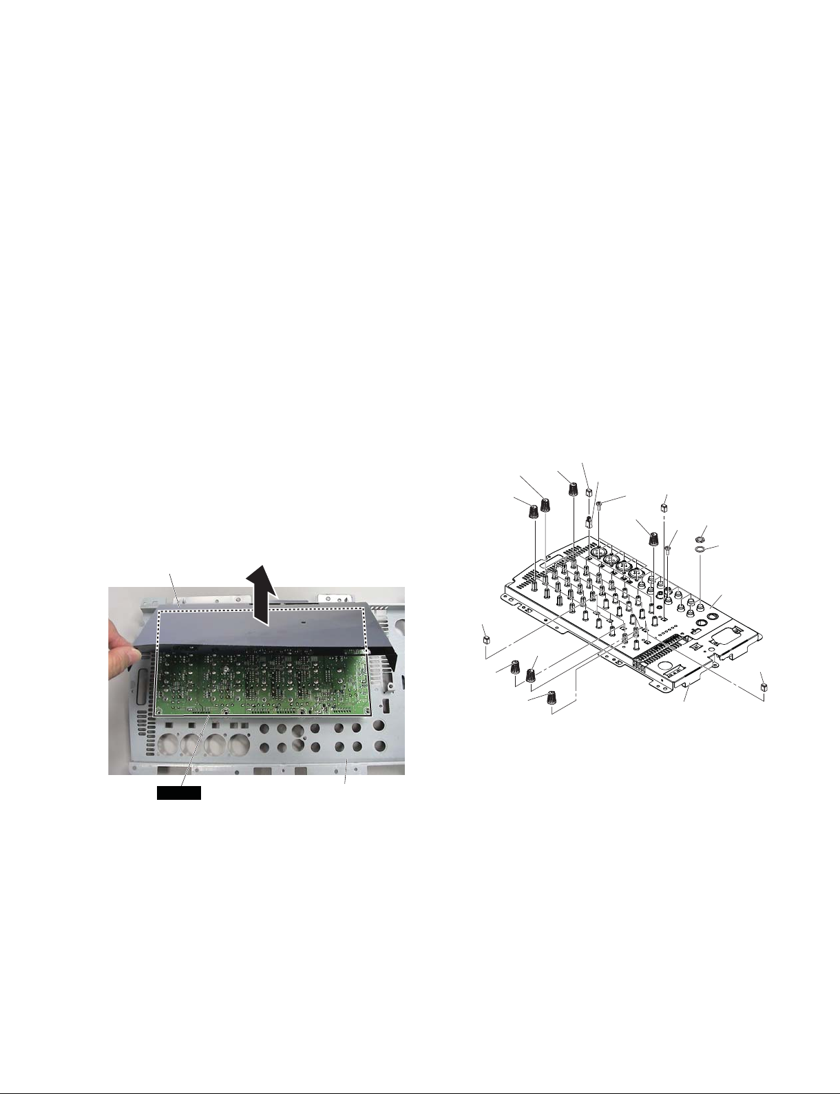
B-9-7-3
Lift the shield mix 6 assembly in the direction of the
arrow as shown in Photo B-1, and remove the fi ve (5)
screws marked [130] and four (4) hexagonal spacers
marked [140]. The MIX62 circuit board can then be
removed. (Fig. B-10, Photo B-1)
* The below parts are not components of the MIX62
circuit board. When replacing the MIX62 circuit board,
remove the below parts from the MIX62 circuit board
and install them to the new circuit board. (Fig. B-11)
[550B] : PUSH BUTTON HPF 6 pcs
[560] : VOLUME KNOB SMALL
(WHITE/BLACK) 8 pcs
[570] : VOLUME KNOB SMALL
(GREEN/BLACK) 22 pcs
[580] : VOLUME KNOB SMALL
(BLUE/BLACK) 5 pcs
[590] : VOLUME KNOB SMALL
(RED/BLACK) 1 pc
* When installing the MIX62 circuit board, tighten the
five (5) screws marked [130] and then the four (4)
hexagonal spacers marked [140].
First tighten the two (2) priority screws in order as
shown in Fig. B-10.
SHIELD MIX 6 ASSEMBLY
(シールドMIX6組立)
STAGEPAS 600i
B-9-7-3
シールド MIX6 組立を写真 B-1 のように矢印の方
向へめくり、[130] のネジ 5 本と [140] の 6 角スペー
サーを 4 本外して、MIX62 シートを外します。
(図 B-10、写真 B-1)
※ 下記の部品は、MIX62 シートの構成部品ではありません。
MIX62 シートを交換する際には、MIX62 シートから下
記の部品を取り外して、新しいシートに取り付けてくだ
さい。(図 B-11)
[550B]: ボタン HPF 6 個
[560]: ノブ VR小(白/黒)8個
[570]: ノブ VR小(緑/黒)22個
[580]: ノブ VR小(青/黒)5個
[590]: ノブ VR小(赤/黒)1個
※ MIX62 シートを取り付けるときには、[130] のネジ 5 本
を締めてから [140] の 6 角スペーサー 4 本を締めてくだ
さい。
このとき、優先ネジ 2 本を図に示す順で先に締めてくだ
さい。(図 B-10)
[550A]
[570]
[580]
[560]
[550B]
[150]
[540]
[560]
[550B]
[540]
[A]
[B]
Panel side
(パネル面)
MIX62
MIXER PANEL 6 ASSEMBLY
(MIXパネル6組立)
Photo B-1
(写真B-1)
[570]
[590]
[580]
MIXER PANEL 6 ASSEMBLY
(MIXパネル6組立)
Fig.B-11
(図B-11)
[550B]
21
STAGEPAS 600i
LSI PIN DESCRIPTION(LSI 端子機能表)
AK5386VT (YD303A00) ADC (Analog to Digital Converter) ................................................................22
LC87F1HC8AF5BT3WA-2H (YE724A00) USB MICROCONTROLLER .............................................23
LM3S808-IQN50-C2T (YD930A00) MAIN MICROCONTROLLER ......................................................23
MFI341S2162 (YE189A00) iPod/iPhone AUTHENTICATION .............................................................22
PCM1781DBQR (X7375A00) DAC (Digital to Analog Converter) ........................................................24
PCM1803ADBR (X7357B00) ADC (Analog to Digital Converter) ........................................................24
PCM1803DBR (X7357A00) ADC (Analog to Digital Converter) ...........................................................24
WM8524CGEDT/R (YC681B00) DAC (Digital to Analog Converter) ....................................................22
YLD330-EZE2 (YC111A00) LED DRIVER ............................................................................................ 24
YSS952-QZE2A (YE441A00) DSP (SPR-2) (Digital Signal Processor) ............................................... 24
AK5386VT (YD303A00) ADC (Analog to Digital Converter)
PIN
NO.
10
I/O FUNCTIONNAME
1
AINR
2
AINL
3
CKS1
4
VCOM
5
AGND
6
VA
7
VD
8
DGND
9
SDTO
LRCK
I
Rch Analog luput Pin
I
Lch Analog lnput Pin
I
Mode Select 1 Pin
Common Voltage Output Pin Bias voltage of ADC input.
O
A-nalog Ground Pin
Ajnalog Power Supply Pin, +5V
Digita1 Power Supply Pin, +3.3V
Digita1 Ground Pin
Audio Serial Data Clock Pin
O
“L” Output at Power-down mode.
Output Channel Clock Pin
I/O
“L” Output in Master Mode at Power-down mode.
PIN
NO.
11
12
13
14
15
16
MCLK
SCLK
PDN
DIF
CKS2
CKS0
MFI341S2162 (YE189A00) iPod/iPhone AUTHENTICATION
PIN
NO.
10
1
2
3
4
5
6
7
8
9
NC
P4/IRQ
NC
RES
CC
V
NC
NC
NC
NC
NC
I/O FUNCTIONNAME
I/O
-
I
-
-
-
-
-
-
Non connection or connect to ground.
Port / Interrupt request
L-channel analog common mode voltage (2.5 V)
Reset
Power supply voltage
Non connection or connect to ground.
PIN
NO.
11
12
13
14
15
16
17
18
19
20
SS
V
P2/IRQ
P1/IRQ
P3/IRQ
NC
NC
NC
NC
NC
NC
I/O FUNCTIONNAME
I/O
I/O
I/O
DSP: IC401
I/O FUNCTIONNAME
I
Master Clock lnput Pin
I/O
Audio Serial Data Clock Pin
“L” Output in Master Mode at Power-down mode.
I
Power Down & Reset Mode Pin
“H”: Power up, “L”: Power down & Reset
The AK5386 must be reset once upon power-up
Audio lnterface Format Pin
I
“H”: 24bit l2S Compatible, “L”: 24bit MSB justified
Mode Select 2 Pin
I
I
Mode Select 0 Pin
DSP: IC602
-
-
-
-
-
-
-
Ground
Port / Interrupt request
Non connection or connect to ground.
.
WM8524CGEDT/R (YC681B00) DAC (Digital to Analog Converter)
22
PIN
NO.
1
2
3
4
5
6
7
8
LINEVOUTL
CPVOUTN
CPCB
LINEGND
CPCA
LINEVDD
DACDAT
LRCLK
I/O FUNCTIONNAME
O
Left line output
O
Charge Pump negative rail decoupling pin
O
Charge Pump fly back capacitor pin
-
Charge Pump ground
O
Charge Pump fly back capacitor pin
-
Charge Pump supply
I
Digital audio interface data input
I
Digital audio interface left/right clock
PIN
NO.
9
10
11
12
13
14
15
16
BCLK
MCLK
MUTE
AIFMODE
AGND
VMID
AVDD
LINEVOUTR
DSP: IC406, IC603
I/O FUNCTIONNAME
I
Digital audio interface bit clock
I
Master clock
I
0 = Mute enabled, 1 = Mute disabled
I
0 = 24-bit Left Justified, 1 = 24-bit I2S, Z = 24-bit Right Justified
-
Analogue ground
O
Analogue midrail decoupling pin
-
Analogue supply
O
Right line output
STAGEPAS 600i
LC87F1HC8AF5BT3WA-2H (YE724A00) USB MICROCONTROLLER
PIN
NO.
1
2
3
4
5
6
7
8
9
10
11
12
13
14
15
16
17
18
19
20
21
22
23
24
25
26
27
28
29
30
P73
RES
XT1
XT2
V
SS1
CF1
CF2
VDD1
SO0
SI0
SCK0
SO1
SI1
SCK1
P16
P17
PWM1
PWM0/MCLKO
VDD2
VSS2
P00
P01
P02
P03
P04
SDAT
BCLK
LRCK
P20
P21
I/O FUNCTIONNAME
I/O
I/O
I/O
I/O
I/O
I/O
I/O
I/O
I/O
I/O
I/O
I/O
I/O
I/O
I/O
I/O
I/O
I/O
I/O
I/O
I/O
I/O
INT3 input (input with noise filter)/timer 0 event input/
timer 0H capture input/IR remote controller receiver input
Reset pin
I
General-purpose input port
I
General-purpose I/O
- Power supply
Ceramic/crystal resonator input
I
Ceramic/crystal resonator output
O
+ Power supply
SIO0 data output
SIO0 data input/bus input/output
SIO0 clock input/output
SIO1 data output
SIO1 data input/bus input/output
SIO1 clock input/output
Timer 1 PWML output
Timer 1 PWMH output/beeper output
Audio interface master clock output
Audio interface master clock output
+ Power supply
-
- Power supply
-
AD converter input ports
AD converter input ports
Onchip debugger pins
System clock output/audio interface SDAT input/output
Timer 6 toggle output/audio interface BCLK input/output
Timer 7 toggle output/audio interface LRCK input/output
INT4 input/HOLD reset input/timer 1 event input/
timer 0L capture input/timer 0H capture input
INT6 input/timer 0L capture 1 input
INT4 input/HOLD reset input/timer 1 event input/
timer 0L capture input/timer 0H capture input
PIN
NO.
31
32
33
34
35
36
37
38
39
40
41
42
43
44
45
46
47
48
P22
P23
P24
P25
P26
P27
UHD-
UHD+
VDD3
VSS3
UFILT
AFILT
P32
URX1
UTX1
P70
P71
P72
I/O FUNCTIONNAME
I/O
I/O
I/O
I/O
I/O
I/O
I/O
I/O
I/O
I/O
I/O
I/O
I/O
I/O
I/O
I/O
INT4 input/HOLD reset input/timer 1 event input/
timer 0L capture input/timer 0H capture input
SIO4 data input/output/parallel interface RD output
INT4 input/HOLD reset input/timer 1 event input/
timer 0L capture input/timer 0H capture input
SIO4 data input/output/parallel interface WR output
INT5 input/HOLD reset input/timer 1 event input/
timer 0L capture input/timer 0H capture input
SIO4 clock input/output/INT7 input/timer 0H capture 1 input
INT5 input/HOLD reset input/timer 1 event input/
timer 0L capture input/timer 0H capture input
SIO9 data input/output/parallel interface RD9 output
INT5 input/HOLD reset input/timer 1 event input/
timer 0L capture input/timer 0H capture input
SIO9 data input/output/parallel interface WR9 output
INT5 input/HOLD reset input/timer 1 event input/
timer 0L capture input/timer 0H capture input
SIO9 clock input/output
USB data I/O pin UHD-/general-purpose I/O port
USB data I/O pin UHD+/general-purpose I/O port
-
USB reference voltage
-
- Power supply
USB interface PLL filter pin
Audio interface PLL filter pin
UART1 receive
UART1 transmit
INT0 input/HOLD reset input/timer 0L
capture input/watchdog timer output
INT1 input/HOLD reset input/timer 0H capture input
INT2 input/HOLD reset input/timer 0 event input/
timer 0L capture input/high speed clock counter input
DSP: IC601
LM3S808-IQN50-C2T (YD930A00) MAIN MICROCONTROLLER
PIN
NO.
1
2
3
4
5
6
7
8
9
10
11
12
13
14
15
16
17
18
19
20
21
22
23
24
25
ADC0
ADC1
ADC2
ADC3
RST
LDO
VDD
GND
OSC0
OSC1
PC7/CCP4
PC6/CCP3
PC5/CCP1
PC4
VDD
GND
PA0/
U0Rx
PA1/
U0Tx
PA2/SSIClk
PA3/SSIFss
PA4/
SSIRx
PA5/
SSITx
VDD
GND
PD0
I/O FUNCTIONNAME
I/O
I/O
I/O
I/O
I/O
I/O
I/O
I/O
I/O
I/O
I/O
I
Analog Analog-to-digital converter input 0.
I
Analog Analog-to-digital converter input 1.
I
Analog Analog-to-digital converter input 2.
I
Analog Analog-to-digital converter input 3.
I
TTL System reset input.
-
Low drop-out regulator output voltage.
pin requires an external capacitor between
the pin and GND of 1 μF or greater.
-
Power Positive supply for I/O and some logic.
-
Power Ground reference for logic and I/O pins.
I
Analog Main oscillator crystal input or an
external clock reference input.
Main oscillator crystal output. Leave unconnected
O
when using a single-ended clock source.
GPIO port C bit 7./Capture/Compare/PWM 4.
GPIO port C bit 6./Capture/Compare/PWM 3.
GPIO port C bit 5./Capture/Compare/PWM 1.
GPIO port C bit 4.
Positive supply for I/O and some logic.
Ground reference for logic and I/O pins.
GPIO port A bit 0./
UART module 0 receive.
I
GPIO port A bit 1./
UART module 0 transmit.
O
GPIO port A bit 2./SSI clock.
GPIO port A bit 3./SSI frame.
GPIO port A bit 4./
SSI receive.
I
GPIO port A bit 5./
SSI transmit.
O
Positive supply for I/O and some logic.
Ground reference for logic and I/O pins.
GPIO port D bit 0.
This
PIN
NO.
26
27
28
29
PB0/CCP0
30
PB1/CCP2
31
32
33
PB2/I2CSCL
34
PB3/I2CSDA
35
36
37
TDO/SWO
38
39
SWDIO/TMS
40
SWCLK/TCK
41
42
43
PB5/CCP5
44
45
46
47
48
PD1
PD2/
U1Rx
PD3/
U1Tx
GND
VDD
PE0
PE1
PC3/
PC2/
TDI
PC1/
PC0/
PB7/
TRST
PB6/
C0+
PB4/
C0ADC7
ADC6
ADC5
ADC4
I/O FUNCTIONNAME
I/O
I/O
I
I/O
O
I/O
I/O
-
I/O
I/O
I/O
I/O
I/O
O
I/O
I
I/O
I/O
I
I/O
I
I/O
I
I/O
I/O
I
I
I
I
I
DSP: IC505
GPIO port D bit 1.
GPIO port D bit 2./
UART module 1 receive.
GPIO port D bit 3./
UART module 1 transmit.
GPIO port B bit 0./Capture/Compare/PWM 0.
GPIO port B bit 1./Capture/Compare/PWM 2.
Ground reference for logic and I/O pins.
Positive supply for I/O and some logic.
GPIO port B bit 2./I2C clock.
GPIO port B bit 3./I2C data.
GPIO port E bit 0.
GPIO port E bit 1.
GPIO port C bit 3./
JTAG TDO and SWO.
GPIO port C bit 2.
JTAG TDI.
GPIO port C bit 1./
JTAG TMS and SWDIO.
GPIO port C bit 0.
JTAG/SWD CLK.
GPIO port B bit 7.
JTAG TRST.
GPIO port B bit 6.
Analog comparator 0 positive input.
GPIO port B bit 5./Capture/Compare/PWM 5.
GPIO port B bit 4.
Analog comparator 0 negative input.
Analog-to-digital converter input 7.
Analog-to-digital converter input 6.
Analog-to-digital converter input 5.
Analog-to-digital converter input 4.
23
STAGEPAS 600i
PCM1781DBQR (X7375A00) DAC (Digital to Analog Converter)
PIN
NO.
I/O FUNCTIONNAME
1
FMT
2
DEMP0
3
DEMP1
4
MUTE
5
SCK
6
DATA
7
BCK
8
LRCK
I
Data format select
I
De-emphasis control
I
De-emphasis control
I
Soft mute control
I
System clock input
I
Audio data digital input
I
Audio data bit clock input
I
Audio data left and right clock input
PIN
NO.
10
11
12
13
14
15
16
9
TEST
NC
V
cc
AGND
VCOM
VOUTR
VOUTL
ZEROA
PCM1803DBR (X7357A00) ADC (Analog to Digital Converter)
PCM1803ADBR (X7357B00) ADC (Analog to Digital Converter)
PIN
NO.
10
1
2
3
4
5
6
7
8
9
VINL
VINR
VREF1
VREF2
V
CC
AGND
PDWN
BYPAS
TEST
LRCK
I/O FUNCTIONNAME
I/O
I
Analog input (L ch)
I
Analog input (R ch)
-
Reference-voltage-1 decoupling capacitor
-
Reference-voltage-2 decoupling capacitor
-
Analog power supply +5V
-
Analog ground
I
Power-down control, active-low
I
HPF bypass control
I
Test, must be connected to DGND
Audio data latch enable input/output
PIN
NO.
11
12
13
14
15
16
17
18
19
20
BCK
DOUT
DGND
DD
V
SCKI
OSR
FMT0
FMT1
MODE0
MODE1
I/O FUNCTIONNAME
I/O
O
-
I
I
I
I
I
I
YLD330-EZE2 (YC111A00) LED DRIVER
PIN
NO.
I/O FUNCTIONNAME
1
GND
2
SDI
3
CLK
4
LD
5
OUTN0
6
OUTN1
7
OUTN2
8
OUTN3
I/O
Ground
Serial Data Input
Serial Data Clock
I
Serial Data Load
I
Output Current Drivers
I
Output Current Drivers
O
Output Current Drivers
O
Output Current Drivers
O
PIN
NO.
10
11
12
13
14
15
16
9
OUTN4
OUTN5
OUTN6
OUTN7
OEN
SDO
REXT
VDD
I/O FUNCTIONNAME
-
Test pin for factory use. Must be LOW or open
-
No connection
-
Power supply, +5V
-
Ground
-
Common voltage decoupling
O
Analog output for R-channel
O
Analog output for L-channel
O
Zero flag output for L- and R-channels
Audio data bit clock input/output
Audio data digital output
Digital ground
Digital power supply +3.3V
System clock input
Oversampling ratio select input
Audio data format select input 0
Audio data format select input 1
Mode select input 0
Mode select input 1
I/O FUNCTIONNAME
O
Output Current Drivers
Output Current Drivers
O
Output Current Drivers
O
Output Current Drivers
O
Output Enable
I
Serial Data Output
O
External Resistor Connection
I
Positive Supply Voltage
-
DSP: IC407
DSP: IC402
MIX62: IC951
YSS952-QZE2A (YE441A00) DSP (SPR-2) (Digital Signal Processor)
24
PIN
NO.
10
11
12
13
14
15
16
1
2
3
4
5
6
7
8
9
GPIO5
GPIO4
GPIO3
DVSS
GPIO2
GPIO1
GPIO0
PLLVDD
IC_N
PLLVSS
PLLVSS
XIN
XOUT
IOVDD
SCL
SDA
I/O FUNCTIONNAME
I/O
General-purpose I/O pins
I/O
I/O
GND
I
General-purpose I/O pins
I
I
PLL power supply
Hardware reset pin
I
PLL GND
Clock input pin
I
Clock output pin
O
Control interface power supply
-
2
I
I
C control bus clock input pin
2
I/O
I
C control bus data I/O pin
PIN
NO.
17
18
19
20
21
22
23
24
25
26
27
28
29
30
31
32
OPEN
DVSS
IRQ_N
DVDD18
GPIO11
TESTb
DVSS
OPEN
DVSS
GPIO10
GPIO9
GPIO8
IOVDD
GPI07
DVDD18
GPI06
I/O FUNCTIONNAME
I/O
I/O
I/O
I/O
I/O
I/O
Leave this pin open
GND
-
O
Interrupt request output pin to the host controller
-
Core power supply
General-purpose I/O pins
I
Test pin
-
GND
-
Leave this pin open
-
GND
General-purpose I/O pins
-
Control interface power supply
General-purpose I/O pins
-
Core power supply
General-purpose I/O pins
DSP: IC403
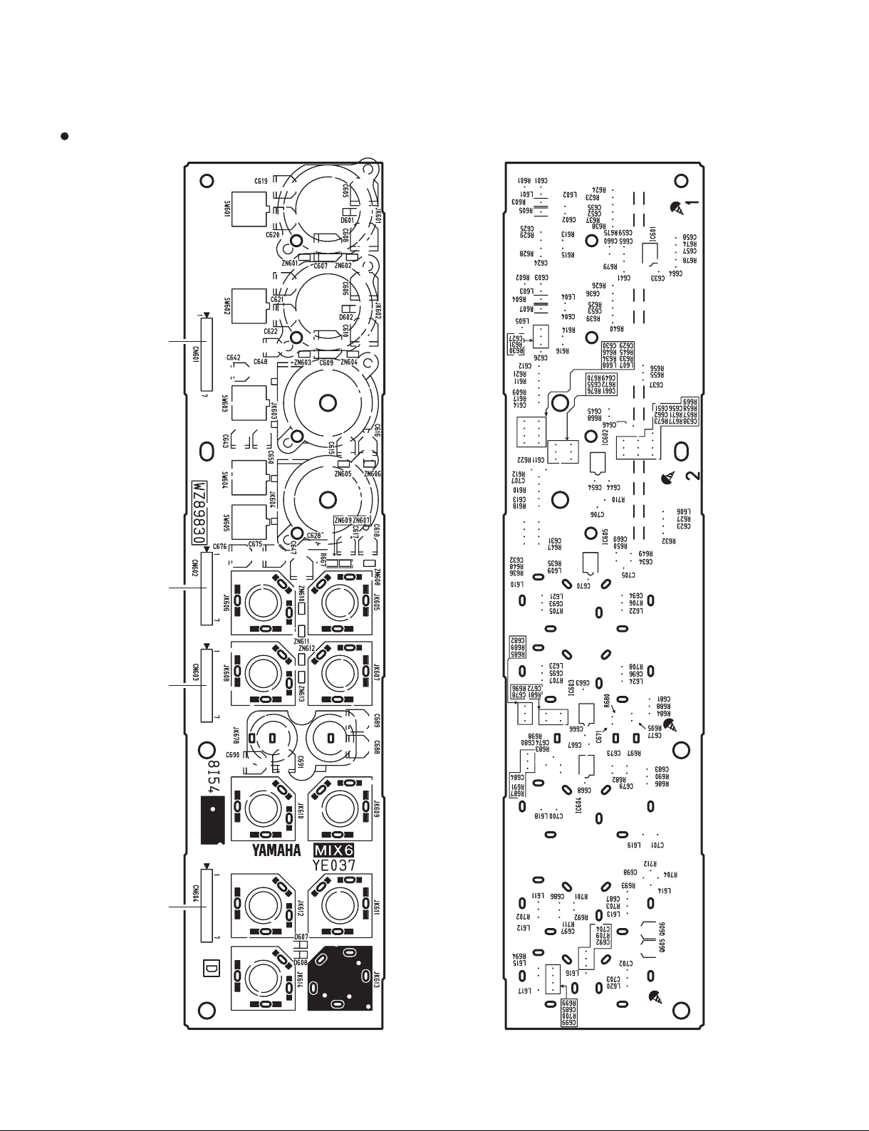
CIRCUIT BOARDS(シート基板図)
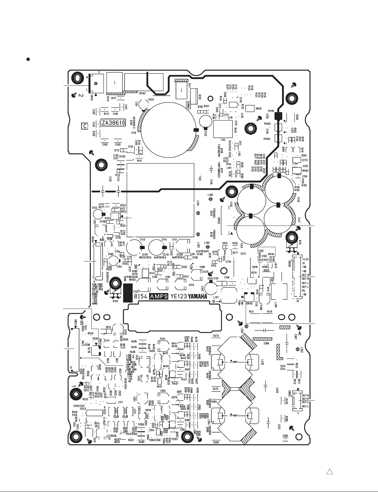
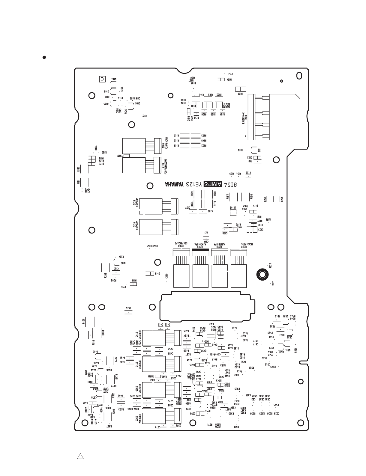
AMPS Circuit Board (YE123C0) .........................................................................26/27
DSP Circuit Board (YE102C0) .................................................................................31
MIX61 Circuit Board (YE037D0) ..............................................................................30
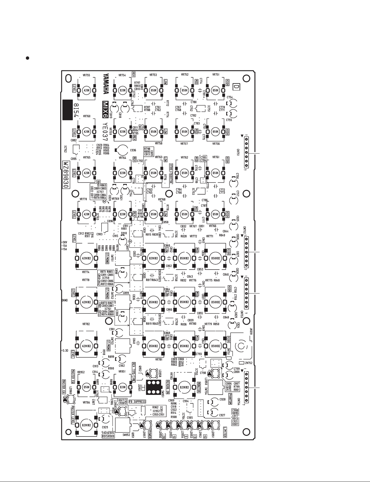
MIX62 Circuit Board (YE037D0) .........................................................................28/29
NET61 Circuit Board (YE176D0) .............................................................................25
NET62 Circuit Board (YE176D0) .............................................................................25
SUB61 Circuit Board (YE117E0) .............................................................................32
SUB62 Circuit Board (YE117E0) .............................................................................33
SUB63 Circuit Board (YE117E0) .............................................................................33
Note: See parts list for details of circuit board component parts.
注 : シートの部品詳細はパーツリストをご参照ください。
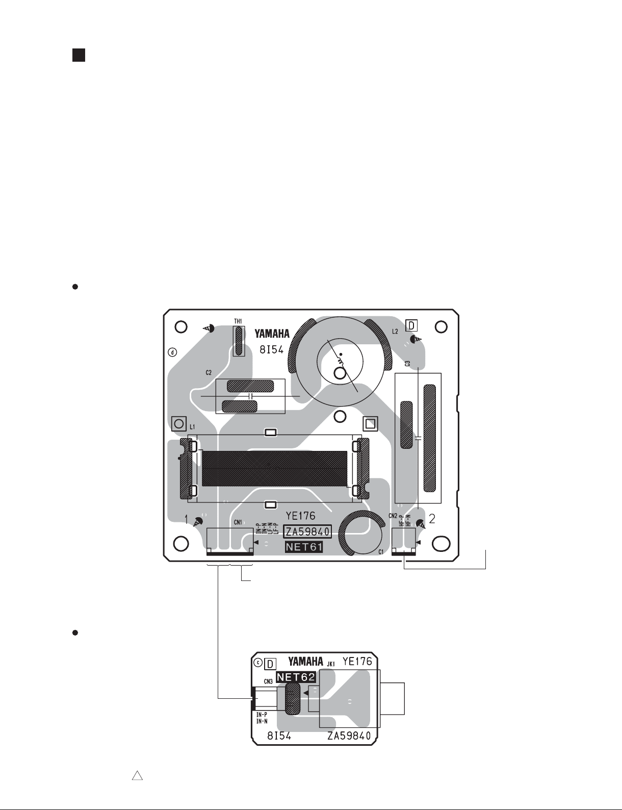
NET61 Circuit Board
STAGEPAS 600i
NET62 Circuit Board
2NA-ZA59840
2
(3-4Pin)
(1-2Pin)
to LOUD SPEAKER (WOOFER)
to LOUD SPEAKER
(TWEETER)
Component side
Component side
(部品側)
(部品側)
25
STAGEPAS 600i
AMPS Circuit Board
to SUB61-W251L
SUB61-W251N
Scale: 90/100
N.C.
to DSP-CN506
N.C.
to DSP-CN505
to SUB63 CN342
to FAN
to SUB63 CN341
26
Component side
2NA-ZA38610
(部品側)
1
STAGEPAS 600i
AMPS Circuit Board
Scale: 90/100
2NA-ZA38610
Pattern side
1
(パターン側)
27
STAGEPAS 600i
MIX62 Circuit Board
Scale: 90/100
to MIX61-CN601
to MIX61-CN602
to MIX61-CN603
to MIX61-CN604
28
Component side
2NA-WZ89830
(部品側)
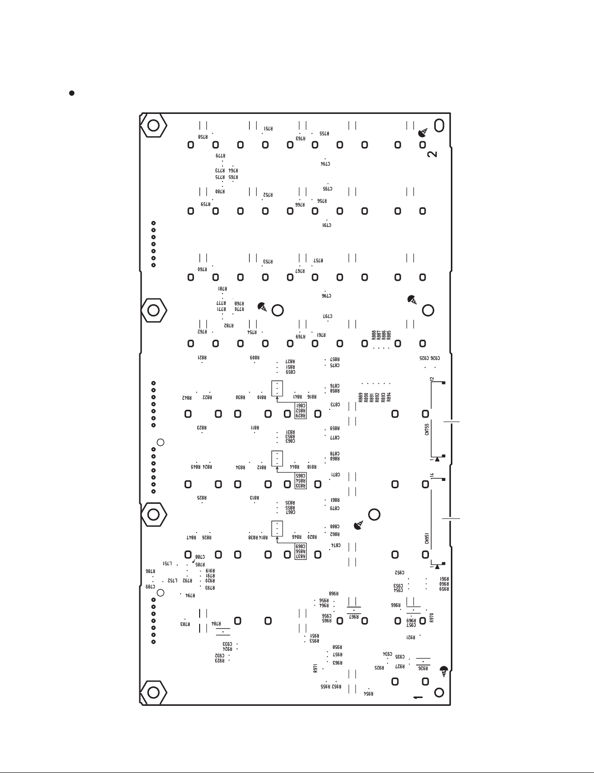
MIX62 Circuit Board
STAGEPAS 600i
to DSP-CN401
to DSP-CN502
2NA-WZ89830
Pattern side
(パターン側)
29
STAGEPAS 600i
MIX61 Circuit Board
to MIX62-CN751
to MIX62-CN752
to MIX62-CN753
to MIX62-CN754
30
Component side
(部品側)
Pattern side
(パターン側)
2NA-WZ89830

DSP Circuit Board
STAGEPAS 600i
N.C. N.C. N.C.
to AMPS-CN511
CN501 (No Mount):
*
Running change on Jan. 2013 production.
(2013年1月生産ランニングチェンジ )
to AMPS-CN104
*
to MIX62-CN755 to MIX62-CN951
Component side
to SUB62-CN301
(部品側)
2NA-ZA32470
Pattern side
1
(パターン側)
31

STAGEPAS 600i
SUB61 Circuit Board
to AMPS-CN101
Component side
(部品側)
32
Pattern side
(パターン側)
2NA-ZA38150
3

SUB62 Circuit Board
to DSP-CN601
STAGEPAS 600i
SUB63 Circuit Board
Component side
(部品側)
to AMPS-CN106
2NA-ZA38150
Pattern side
3
(パターン側)
to AMPS-CN351
Component side
(部品側)
Pattern side
(パターン側)
33

STAGEPAS 600i
TEST PROGRAM
(テストプログラム)
This test program is applied to the STAGEPAS 600i.
1. Preparation
1-1. Required items
• Personal Computer
DOS/V machine 1 unit
Windows XP SP3 with COM port
(CPU Pentium 500 MHz or above, RAM 256 MB or above)
Windows 7 with COM port
(CPU multi core 1.0 GHz or above,
RAM 1 GB(32 bit)/2 GB(64 bit) or above)
• Serial interface jig set for diagnosis : ZF928400
(USB2UART-CP2102) x 1
A2-SH cable x 1
• USB cable x 1
• iPhone/iPod
If the operation system is Windows XP, download the
USB-UART conversion jig driver from the YSISS
homepage.
*For Windows 7, it is recognized as the COM port.
1-2. Application for Service inspection
Download the latest version of application fi les for service
inspection from the YSISS homepage and copy them to C
drive of personal computer as shown below.
(URL >> http://plaza.yamaha.co.jp/ysiss/exindex.nsf)
•
C:¥Stagepas¥tools¥Diag¥DiagSTAGEPASII-SERVICE.exe
•
C:¥Stagepas¥tools¥Diag¥DiagSTAGEPASII-SERVICE.ini
These are used for displaying the instruction of test
execution and the result of execution.
このテストプログラムは STAGEPAS600i に適用されます。
1. 準備
1-1. 必要なもの
•
パソコン
DOS/V 機1台
WindowsXPSP3COM ポート有り
(CPUPentium500MHz 以上、RAM256MB 以上 )
Windows7COM ポート有り
(CPU マルチコア1.0GHz 以上、
RAM1GB 以上 (32bit)/2GB(64bit) 以上 )
• ダイアグ用シリアルインターフェース治具セッ
ト:ZF928400
(USB2UART-CP2102)×1
A2-SHケーブル×1
• USBケーブル×1
• iPhone/iPod ×1
OS が XP の場合 は、USB-UART 変換治具のドラ
イバーを YSISS ホームページからダウンロードし
てください。
※ Windows7 では COM ポートと認識されます。
1-2. サービス検査用アプリケーション
YSISS ホームページからサービス検査用アプリケー
ションファイル最新版をダウンロードし、パソコンの
C ドライブに下記のようにコピーします。
(URL >> http://plaza.yamaha.co.jp/ysiss/index.nsf)
C:¥Stagepas¥tools¥Diag¥DiagSTAGEPASII-SERVICE.exe
•
•
C:¥Stagepas¥tools¥Diag¥DiagSTAGEPASII-SERVICE.ini
これらはテスト実行指示と実行結果を表示するために
使用します。
1-3. Connection
Perform connection as shown in the fi gure below.
USB cable
(USBケーブル)
PC
MIXER ASSEMBLY
1-3. 接続
下図のように接続します。
Serial interface jig set for diagnosis
(ダイアグ用シリアルインターフェース 治 具セット)
(USB2UART-CP2102)
(4P)
(4P)
CN504
(4P)
DSP
A2-SH cable
(A2-SH ケーブル)
CN503
(4P)
: ZF928400
iPod/iPhone
34

STAGEPAS 600i
2. Service inspection
2-1. How to activate
(1) Turn on the mixer 600 assembly while pushing the
REVERB ON switch.
About 4 seconds later, the diagnostic mode is activat-
ed, and all the LEDs on the panel are turned on (except
LED “PHANTOM CH1/2”).
(2) Run application for Service inspection (Diag-
STAGEPASII-SERVICE.exe).
The following inspection screen is displayed.
Note:
If not all the LEDs on the panel are turned on, it may
be considered that a mode other than the diagnostic
mode is activated, the location of installation is mistaken, or there is a malfunction of peripheral circuitry.
Inspection screen (検査画面)
3. Start inspection.
検査を開始します。3.
2. サービス検査
2-1. 起動方法
(1)REVERB ON スイッチを押した状態でミキサー
Ass'y の電源を入れます。
約 4 秒後、ダイアグモードが起動し、パネル
のLEDが全点灯します。(LED"PHANTOM
CH1/2" は除きます。)
(2)サービス検査用アプリケーション(DiagSTAGE-
PASII-SERVICE.exe)を起動します。
注:
パネルの LED が全点灯しない場合、ダイアグ
モード以外のモードで起動したか、設置ミスま
たは周辺回路の故障が考えられます。
1. Select “STAGEPASII-SERVICE”.
3. Start inspection.
3.検査を開始します。
択。選を」STAGEPASII-SERVICE「.1
2. Tick all.
2.全てにチェックを入れます。
* The DC-PROTECTION inspection is removed for the
default in order to operate an inner terminal.
2. Tick also detailed inspection items.
2.詳細項目にもチェックをいれます。
※ DC-PROTECTION 検 査は、内部端子を操作す
るため、デフォルト対象からはずしてあります。
35

STAGEPAS 600i
3. Test Items
For details of inspection refer to “INSPECTIONS” on
page 52.
3-1. INFO inspection
Check VERSION number and MODEL ID by sight.
The result is displayed in property window as shown below.
* It’s possible that the column of value is in blank.
* Example is described in the column of Value.
* If firmware is broken, “firmware is broken” is
displayed in VERSION.
Field
VERSION V0.30 Character string of Version.
MODEL ID STAGEPAS600i Corresponding Model ID.
Troubleshooting
Check signal line between SW (DSP circuit board: SW701)
and CPU (DSP circuit board: IC701), and SW itself.
3-2. DSP inspection
Communication condition with DSP via I2C-BUS and
operational state of inside DSP are inspected automatically.
The result is displayed in output window as shown below.
Value
(Example)
Supplementary note
3. 検査項目
検査の詳細は「検査」(52 ページ)を参照してくだ
さい。
3-1. INFO 検査
VERSION 番号、MODELID を目視で確認します。
検査結果はプロパティウインドウへ下記のように表
示されます。
※Value の欄が空白の場合もありえます。
※Value の欄には、例を記入してあります。
※ファームウェアが破壊している場合、「VER-
SION」に「firmwareisbroken」と表示されます。
Field
VERSION V0.30 バージョン文字列
MODELID STAGEPAS600i 該当するモデル ID
トラブルシューティング
DSP シートと AMPS シートの接続、AMPS シート
上の DC 検出回路を確認してください。
3-2. DSP 検査
I2C-BUS経由の DSPとの通信状態、DSP 内部の
動作状態の良否を自動的に検査します。
検査結果はアウトプットウインドウへ下記のように
表示されます。
Value
(例)
補足
When Normal
I2C DSP COM PASS: DSP COMMUNICATION
I2C DSP CTRL PASS: DSP CONTROL
When out of order
I2C DSP COM FAIL: DSP COMMUNICATION
I2C DSP CTRL FAIL: DSP CONTROL
Troubleshooting
If “FAIL: DSP COMMUNICATION” is indicated, check
wire connection and the following parts: DSP (DSP circuit board: IC403) and CPU (DSP circuit board: IC505)
3-3. AD input port inspection
The voltage (temperature) from T-SENSE port and the
voltage from V-BUS port are inspected automatically.
● T-SENSE port
The result is displayed in output window as shown below.
When Normal
0.65V
~
1.37V
PASS: Temperature (x.xx V)
When Abnormal
0.64 V or below FAIL: Temperature *(x.xx V)
1.38 V or above FAIL: Temperature *(x.xx V)
*(x.xxV) represents electric pressure (temperature) measured.
正常時
I2C DSPCOM PASS:DSPCOMMUNICATION
I2C DSPCTRL PASS:DSPCONTROL
故障時
I2C DSPCOM FAIL:DSPCOMMUNICATION
I2C DSPCTRL FAIL:DSPCONTROL
トラブルシューティング
FAIL:DSPCOMMUNICATIONと表示されて
いる場合、結線及び下記の部品を確認してください。
DSP(DSP シート:IC403)と CPU(DSP シート:
IC505)
3-3. AD入力ポート検査
T-SENSEポートからの電圧(温度)、V-BUS ポー
トからの電圧を自動的に検査します。
● T-SENSEport
検査結果はアウトプットウインドウへ下記のように
表示されます。
正常時
0.65V 〜 1.37V
PASS:Temperature*(x.xxV)
異常時
0.64V以下 FAIL:Temperature*(x.xxV)
1.38V以上 FAIL:Temperature*(x.xxV)
*(x.xxV) は、測定した電圧 ( 温度 ) を表示します。
36

STAGEPAS 600i
● V-BUS port
The result is displayed in output window as shown below.
When Normal
2.50V
~
2.70V
PASS: V-SUB *(x.xx V)
When Abnormal
2.49 V or below FAIL: V-SUB *(x.xx V)
2.71 V or above FAIL: V-SUB *(x.xx V)
*(x.xxV) represents electric pressure measured.
3-4. LED inspection
LIMIT LED lights. J Conduct inspection whether it turns
off the light.
SIGNAL LED lights. J Conduct inspection whether it
turns off the light.
POWER LED lights. J Conduct inspection whether it
turns off the light.
REVERB-ON LED lights. → Conduct inspection whether
it turns off the light.
FBS LED lights. → Conduct inspection whether it turns off
the light.
BOOST LED lights. → Conduct inspection whether it
turns off the light.
Conduct inspection whether all LEDs light or not.
* FBS = FEEDBACK-SUPRESSOR
● V-BUSport
検査結果はアウトプットウインドウへ下記のように
表示されます。
正常時
2.50V 〜 2.70V
PASS: V-SUB *(x.xx V)
異常時
2.49V以下
2.71V以上
FAIL: V-SUB *(x.xx V)
FAIL: V-SUB *(x.xx V)
*(x.xxV) は、測定した電圧を表示します。
3-4. LED検査
LIMITLEDが点灯→消灯するか検査を行います。
SIGNALLEDが点灯→消灯するか検査を行います。
POWERLEDが点灯→消灯するか検査を行います。
REVERB-ONLED が点灯→消灯するか検査を行い
ます。
FBSLEDが点灯→消灯するか検査を行います。
BOOSTLEDが点灯→消灯するか検査を行います。
全 LEDが点灯するか検査を行います。
Click “OK” button and each LED test is started.
In consideration of a case that operator misses a sequence
of action that turns on J off the LED, it’s possible to
reconfi rm the successive test with “Retry” button.
「OK」ボタンをクリックして、各 LED テストを開
始します。
オペレータが LED の点灯→消灯を見逃すケースを
考慮し、「Retry」ボタンでの一連のテストの再確認
が可能です。
37

STAGEPAS 600i
Determine all LED tests comprehensively.
If result is PASS, click “Yes” button.
If result is FAIL, click “No” button.
The result is displayed in output window as shown below.
When Normal
LIMIT LED PASS: LIMIT LED
SIGNAL LED PASS: SIGNAL +6/+3/0/-6/-20 LED
POWER LED PASS: POWER LED
REVERB-ON LED PASS: REVERB-ON LED
FBS LED PASS: FBS LED
BOOST LED PASS: BOOST LED
LED ALL PASS: LED ALL
全 LED テストの総合判定を行います。
結果が PASS の場合、「Yes」ボタンをクリックし
ます。
結果が FAIL の場合、「No」ボタンをクリックします。
検査結果はアウトプットウインドウへ下記のように
表示されます。
正常時
LIMIT LED PASS: LIMIT LED
SIGNAL LED PASS: SIGNAL +6/+3/0/-6/-20 LED
POWER LED PASS: POWER LED
REVERB-ON LED PASS: REVERB-ON LED
FBS LED PASS: FBS LED
BOOST LED PASS: BOOST LED
LED ALL PASS: LED ALL
When out of order
LIMIT LED FAIL: LIMIT LED
SIGNAL LED FAIL: SIGNAL +6/+3/0/-6/-20 LED
POWER LED FAIL: POWER LED
REVERB-ON LED FAIL: REVERB-ON LED
FBS LED FAIL: FBS LED
BOOST LED FAIL: BOOST LED
LED ALL FAIL: LED ALL
3-5. JACK inspection
The connection inspection of SUBWOOFER OUT jack is
conducted.
The connection inspection of REVERB FOOT SW jack is
conducted.
[SUBWOOFER OUT]
Once the headphone jack is attached to the SUBWOOFEROUT terminal, click “OK” button.
故障時
LIMIT LED FAIL: LIMIT LED
SIGNAL LED FAIL: SIGNAL +6/+3/0/-6/-20 LED
POWER LED FAIL: POWER LED
REVERB-ON LED FAIL: REVERB-ON LED
FBS LED FAIL: FBS LED
BOOST LED FAIL: BOOST LED
LED ALL FAIL: LED ALL
3-5. JACK検査
SUBWOOFEROUT 端子の接続検査を行います。
REVERBFOOTSW 端子の接続検査を行います。
[SUBWOOFEROUT]
SUBWOOFER-OUT 端子にヘッドフォンジャック
を取り付けたら、「OK」ボタンをクリックします。
38

STAGEPAS 600i
Once the headphone jack is removed from the
SUBWOOFER-OUT terminal, click “OK” button.
Click “Retry” button if you start the test again.
SUBWOOFER-OUT 端子からヘッドフォンジャッ
クを取り外したら、「OK」ボタンをクリックします。
再テストを実施したいときは、「Retry」ボタンをク
リックします。
[REVERB FOOT SW]
Once the foot switch, which is connected to the REVERB
FOOT SW terminal, is turned on, click “OK” button.
Once the foot switch, which is connected to the REVERB
FOOT SW terminal, is turned off, click “OK” button.
[REVERBFOOTSW]
REVERBFOOT SW 端子に接続したフットスイッ
チを ON にしたら、「OK」ボタンをクリックします。
REVERBFOOT SW 端子に接続したフットスイッ
チを OFFにしたら、「OK」ボタンをクリックします。
39

STAGEPAS 600i
Click “Retry” button if you start the test again.
The result is displayed in output window as shown below.
When Normal
SUBWOOFER OUT
REVERB FOOT SW
PASS: SUBWOOFER-OUT ON
PASS: SUBWOOFER-OUT OFF
PASS: REVERB-FOOT-SW ON
PASS: REVERB-FOOT-SW OFF
When out of order
SUBWOOFER OUT
REVERB FOOT SW
FAIL: SUBWOOFER-OUT ON
FAIL: SUBWOOFER-OUT OFF
FAIL: REVERB-FOOT-SW ON
FAIL: REVERB-FOOT-SW OFF
再テストを実施したいときは、「Retry」ボタンをク
リックします。
検査結果はアウトプットウインドウへ下記のように
表示されます。
正常時
SUBWOOFER OUT
REVERB FOOT SW
PASS: SUBWOOFER-OUT ON
PASS: SUBWOOFER-OUT OFF
PASS: REVERB-FOOT-SW ON
PASS: REVERB-FOOT-SW OFF
故障時
SUBWOOFER OUT
REVERB FOOT SW
FAIL: SUBWOOFER-OUT ON
FAIL: SUBWOOFER-OUT OFF
FAIL: REVERB-FOOT-SW ON
FAIL: REVERB-FOOT-SW OFF
3-6. SWITCH/VOLUME inspection
Inspect on | off status of FBS switch.
Inspect on | off status of REVERB ON switch.
The reading inspection of the maximum and the minimum
of REVERB TYPE volume. (*1)
The reading inspection of the maximum and the minimum
of MASTER EQ volume. (*1)
The reading inspection of the maximum and the minimum
of MASTER LEVEL volume. (*1)
(*1) The maximum is a value when it turns to the end of
the right.
The minimum is a value when it turns to the end of
the left.
[SWITCH]
Set status of each switch according to the display and click
“OK” button.
3-6. SWITCH/VOLUME 検査
FBS スイッチの ON¦OFF状態を検査します。
REVERBON スイッチの ON¦OFF 状態を検査し
ます。
REVERBTYPE ボリュームの最大値・最小値の読
み取り検査を行います。(*1)
MASTEREQ ボリュームの最大値・最小値の読み
取り検査を行います。(*1)
MASTERLEVEL ボリュームの最大値・最小値の
読み取り検査を行います。(*1)
(*1) 最大値は、右方向の突き当たりまで回したとき
の値。
最小値は、左方向の突き当たりまで回したとき
の値。
[SWITCH]
画面表示に従って各スイッチの状態を設定し、「OK」
ボタンをクリックします。
40

STAGEPAS 600i
If result is FAIL, the following display for retry is displayed.
When “Retry” button is clicked, the test is performed
again.
When “Cancel” button is clicked, the test is not performed
again.
FAIL の場合、下記の再検査用画面が表示されます。
「Retry」ボタンをクリックすると再テストが実施さ
れます。
「Cancel」ボタンをクリックすると再テストは実施
されません。
[KNOB(VOLUME)]
The status of each knob is operated according to the display
and click “OK” button.
[KNOB(VOLUME)]
画面表示に従って各ツマミの状態を操作し、「OK」
ボタンをクリックします。
41

STAGEPAS 600i
If result is FAIL, the following display for retry is displayed.
When “Retry” button is clicked, the test is performed
again.
When “Cancel” button is clicked, the test is not performed
again.
FAIL の場合、下記の再検査用画面が表示されます。
「Retry」ボタンをクリックすると再テストが実施さ
れます。
「Cancel」ボタンをクリックすると再テストは実施
されません。
42

STAGEPAS 600i
The result is displayed in output window as shown below.
When Normal
FBS ON SW
REVERB ON SW
REVERB TYPE (VOL)
MASTER EQ (VOL)
MASTER LEVEL (VOL)
PASS: FEEDBACK-SUPPRESSOR ON
PASS: FEEDBACK-SUPPRESSOR OFF
PASS: REVERB-ON-SW ON
PASS: REVERB-ON-SW OFF
PASS: REVERB TYPE Maximum Point (xxx)
PASS: REVERB TYPE Minimum Point (xx)
PASS: MASTER EQ Maximum Point (xxx)
PASS: MASTER EQ Minimum Point (xx)
PASS: MASTER LEVEL Maximum Point (xxx)
PASS: MASTER LEVEL Minimum Point (xx)
When out of order
FBS ON SW
REVERB ON SW
REVERB TYPE (VOL)
MASTER EQ (VOL)
MASTER LEVEL (VOL)
FAIL: FEEDBACK-SUPPRESSOR ON
FAIL: FEEDBACK-SUPPRESSOR OFF
FAIL: REVERB-ON-SW ON
FAIL: REVERB-ON-SW OFF
FAIL: REVERB TYPE Maximum Point (xxx)
FAIL: REVERB TYPE Minimum Point (xx)
FAIL: MASTER EQ Maximum Point (xxx)
FAIL: MASTER EQ Minimum Point (xx)
FAIL: MASTER LEVEL Maximum Point (xxx)
FAIL: MASTER LEVEL Minimum Point (xx)
検査結果はアウトプットウインドウへ下記のように
表示されます。
正常時
FBS ON SW
REVERB ON SW
REVERB TYPE (VOL)
MASTER EQ (VOL)
MASTER LEVEL (VOL)
PASS: FEEDBACK-SUPPRESSOR ON
PASS: FEEDBACK-SUPPRESSOR OFF
PASS: REVERB-ON-SW ON
PASS: REVERB-ON-SW OFF
PASS: REVERB TYPE Maximum Point (xxx)
PASS: REVERB TYPE Minimum Point (xx)
PASS: MASTER EQ Maximum Point (xxx)
PASS: MASTER EQ Minimum Point (xx)
PASS: MASTER LEVEL Maximum Point (xxx)
PASS: MASTER LEVEL Minimum Point (xx)
故障時
FBS ON SW
REVERB ON SW
REVERB TYPE (VOL)
MASTER EQ (VOL)
MASTER LEVEL (VOL)
FAIL: FEEDBACK-SUPPRESSOR ON
FAIL: FEEDBACK-SUPPRESSOR OFF
FAIL: REVERB-ON-SW ON
FAIL: REVERB-ON-SW OFF
FAIL: REVERB TYPE Maximum Point (xxx)
FAIL: REVERB TYPE Minimum Point (xx)
FAIL: MASTER EQ Maximum Point (xxx)
FAIL: MASTER EQ Minimum Point (xx)
FAIL: MASTER LEVEL Maximum Point (xxx)
FAIL: MASTER LEVEL Minimum Point (xx)
3-7. FAN inspection
Inspect FAN condition when the speed of FAN is changed.
Inspect the speed of FAN to change and to become early.
Determine FAN tests comprehensively.
If result is PASS, click “Yes” button.
If result is FAIL, click “No” button.
The result is displayed in output window as shown below.
When Normal
FAN CHECK PASS: FAN CHECK
3-7. FAN検査
FAN の速度を変化させ FANの良否を検査します。
FAN のスピードが変化し早くなることを検査しま
す。
FAN テストの総合判定を行います。
結果が PASS の場合、「Yes」ボタンをクリックし
ます。
結果が FAIL の場合、「No」ボタンをクリックします。
検査結果はアウトプットウインドウへ下記のように
表示されます。
正常時
FAN CHECK PASS: FAN CHECK
When out of order
FAN CHECK FAIL: FAN CHECK
故障時
FAN CHECK FAIL: FAN CHECK
43

STAGEPAS 600i
Troubleshooting
If “FAIL: FAN CHECK” is indicated, check connection
of DSP circuit board and AMPS circuit board, and check
FAN, and power supply circuit of FAN on AMPS circuit
board.
3-8. iPhone/iPod inspection
The authentication and connection check of iPhone/iPod
is done.
The analog characteristics of USB-audio are measured.
(The DSP characteristic is a fl at)
The level check at the time of USB mute (SP OUT side)
is performed. (The DSP characteristic is a fl at)
iPhone/iPod is connected to the USB terminal with the
exclusive USB cable.
iPod must be connected and powered on prior to test execution.
AUTHENTICATION AND CONNECTION CHECK
The connection confi rm of attestation LSI (IC602) and a
USB microcomputer (IC601) is performed.
トラブルシューティング
FAIL:FANCHECKと表示されている場合、
DSP シートと AMPS シートの接続、FAN および
AMPS シート上の FAN の電源回路を確認してくだ
さい。
3-8. iPhone/iPod検査
認証 LSI と USB マイコンの接続確認を行います。
USB-audio のアナログ特性の測定を行います。(DSP
特性はフラット)
USB ミュート時(SPOUT 側)のレベル確認を行
います。(DSP は特性フラット)
テスト実施する前に、iPhone/iPod を専用 USB ケー
ブルで USB 端子に接続しておき、iPhone/iPod の
電源が ON になっていることを確認します。
AUTHENTICATIONANDCONNECTIONCHECK
認証 LSI(IC602) と USB マイコン (IC601) の接続確
認を行います。
USB-SIGNAL-PATH TEST
The measurement result in the reproduction test of a USB
signal path is inputted.
If result is PASS, click “Yes” button.
If result is FAIL, click “No” button.
USB-SIGNAL-PATHTEST
USB 音声経路の再生テストでの計測結果を入力す
る。
結果が PASS の場合、「Yes」ボタンをクリックし
ます。
結果が FAIL の場合、「No」ボタンをクリックします。
44

STAGEPAS 600i
USB-MUTE TEST
The measurement result in the USB-MUTE test of a USB
voice path is inputted.
If result is PASS, click “Yes” button.
If result is FAIL, click “No” button.
DA-MUTE-USB TEST
The measurement result in the DA-MUTE-USB test of a
USB voice path is inputted.
If result is PASS, click “Yes” button.
If result is FAIL, click “No” button.
USB-MUTETEST
USB 音声経路の USB-MUTE テストでの計測結果
を入力します。
結果が PASS の場合、「Yes」ボタンをクリックし
ます。
結果が FAIL の場合、「No」ボタンをクリックします。
DA-MUTE-USBTEST
USB 音声経路の DA-MUTE-USB テストでの計測
結果を入力します。
結果が PASS の場合、「Yes」ボタンをクリックし
ます。
結果が FAIL の場合、「No」ボタンをクリックします。
When determination of the result based on measurement
result by operator is input, the result is displayed in output
window as shown below.
When Normal
AUTHENTICATION PASS: IPOD AUTHENTICATION
USB-SIGNAL-PATH PASS: USB-SIGNAL-PATH LEVEL
USB-MUTE ON
USB-MUTE OFF
DA-MUTE-USB ON
DA-MUTE-USB OFF
PASS: USB-MUTE ON LEVEL
PASS: USB-MUTE OFF LEVEL
PASS: DA-MUTE-USB ON LEVEL
PASS: DA-MUTE-USB OFF LEVEL
When out of order
AUTHENTICATION FAIL: IPOD AUTHENTICATION
USB-SIGNAL-PATH FAIL: USB-SIGNAL-PATH LEVEL
USB-MUTE ON
USB-MUTE OFF
DA-MUTE-USB ON
DA-MUTE-USB OFF
FAIL: USB-MUTE ON LEVEL
FAIL: USB-MUTE OFF LEVEL
FAIL: DA-MUTE-USB ON LEVEL
FAIL: DA-MUTE-USB OFF LEVEL
オペレータの計測結果に応じた結果判定を入力する
と、検査結果はアウトプットウインドウへ下記のよ
うに表示されます。
正常時
AUTHENTICATION PASS: IPOD AUTHENTICATION
USB-SIGNAL-PATH PASS: USB-SIGNAL-PATH LEVEL
USB-MUTE ON
USB-MUTE OFF
DA-MUTE-USB ON
DA-MUTE-USB OFF
PASS: USB-MUTE ON LEVEL
PASS: USB-MUTE OFF LEVEL
PASS: DA-MUTE-USB ON LEVEL
PASS: DA-MUTE-USB OFF LEVEL
異常時
AUTHENTICATION FAIL: IPOD AUTHENTICATION
USB-SIGNAL-PATH FAIL: USB-SIGNAL-PATH LEVEL
USB-MUTE ON
USB-MUTE OFF
DA-MUTE-USB ON
DA-MUTE-USB OFF
FAIL: USB-MUTE ON LEVEL
FAIL: USB-MUTE OFF LEVEL
FAIL: DA-MUTE-USB ON LEVEL
FAIL: DA-MUTE-USB OFF LEVEL
45

STAGEPAS 600i
3-9. ANALOG inspection
The analog characteristics of MAIN path are inspected. (The
DSP characteristic is a fl at)
The analog characteristics of REV-MONITOR path are
inspected. (The DSP characteristic is made into a fl at and a
REV-ADC input is assigned to a Moni-DAC output)
The measurement result in the ANALOG test of a MAIN
path is inputted.
If result is PASS, click “Yes” button.
If result is FAIL, click “No” button.
The measurement result in the ANALOG test of a REVMONITOR path is inputted.
If result is PASS, click “Yes” button.
If result is FAIL, click “No” button.
3-9. ANALOG検査
MAIN経路のアナログ特性の検査を行います。(DSP
特性はフラット)
REV-MONITOR 経路のアナログ特性の検査を行い
ます。(DSP 特性をフラットにし、REV-ADC 入力
を Moni-DAC 出力にアサインします。)
MAIN 経路の ANALOG テストでの計測結果を入力
します。
結果が PASS の場合、「Yes」ボタンをクリックし
ます。結果が FAIL の場合、「No」ボタンをクリッ
クします。
REV-MONITOR 経路の ANALOG テストでの計測
結果を入力します。
結果が PASS の場合、「Yes」ボタンをクリックし
ます。結果が FAIL の場合、「No」ボタンをクリッ
クします。
46
When determination of the result based on measurement
result by operator is input, the result is displayed in output
window as shown below.
When Normal
Measurement value
PA SS
PASS: MAIN ANALOG LEVEL
or
PASS: REV-MONITOR ANALOG LEVEL
When out of order
Measurement value
FAIL
FAIL: MAIN ANALOG LEVEL
or
FAIL: REV-MONITOR ANALOG LEVEL
オペレータの計測結果に応じた結果判定を入力する
と、検査結果はアウトプットウインドウへ下記のよ
うに表示されます。
正常時
計測値 PASS
PASS:MAINANALOGLEVEL
or
PASS:REV-MONITORANALOGLEVEL
異常時
計測値 FAIL
FAIL:MAINANALOGLEVEL
or
FAIL:REV-MONITORANALOGLEVEL

STAGEPAS 600i
●Flow of signal of "MAIN SIGNAL PATH" mode
(The DSP has fl at frequency characteristics. The input/output
patches are the same as the normal mode.)
L
R
REV
ADC
ADC
iPod/iPhone
ADC
ADC
DSP
●本線経路アナログ特性の測定検査
(DSP 特性はフラット。インプット・アウトプットパッ
チは通常モードと同様です。)
DAC
DAC
DAC
DAC
DAC
DAC
DAC
DAC
LPF
LPF
SPEAKER L
SPEAKER R
L/MONO
MONITOR/REC OUT
R
●
Flow of signal of "REV-MONITOR SIGNAL PATH" mode
(The DSP has flat frequency characteristics. It assigns the
REV-ADC input to the Moni-DAC output.)
L
R
REV
iPod/iPhone
ADC
ADC
ADC
ADC
DSP
●REV-MONITOR 経路アナログ特性の測定検査
(DSP 特性はフラット、REV-ADC 入力を Moni-DAC
出力にアサインします。)
DAC
DAC
DAC
DAC
DAC
DAC
DAC
DAC
LPF
LPF
SPEAKER L
SPEAKER R
L/MONO
MONITOR/REC OUT
R
47

STAGEPAS 600i
3-10. A-MUTE inspection
Conduct level check when analog mute (SP OUT side).
Input measuring result on A-MUTE test.
If result is PASS, click “Yes” button.
If result is FAIL, click “No” button.
When determination of the result based on measurement
result by operator is input, the result is displayed in output
window as shown below.
When Normal
Measurement value PASS PASS: A-MUTE LEVEL
3-10. A-MUTE検査
アナログミュート時(SPOUT 側)のレベル確認を
行います。
A-MUTE テストでの計測結果を入力します。
結果が PASS の場合、「Yes」ボタンをクリックし
ます。結果が FAIL の場合、「No」ボタンをクリッ
クします。
オペレータの計測結果に応じた結果判定を入力する
と、検査結果はアウトプットウインドウへ下記のよ
うに表示されます。
正常時
計測値 PASS PASS:A-MUTE LEVEL
When Abnormal
Measurement value FAIL FAIL: A-MUTE LEVEL
Troubleshooting
In FAIL, check IC504 (3, 6pin) on a DSP circuit board,
the parts of the circumference of it, and wiring to an
AMPS circuit board.
3-11. DA-MUTE inspection
Conduct level check when DA mute (SP OUT side).
Simultaneously, Conduct level check when DA mute
(MONITOR OUT side).
Input measuring result on DA-MUTE test.
If result is PASS, click “Yes” button.
If result is FAIL, click “No” button.
異常時
計測値 FAIL FAIL:A-MUTE LEVEL
トラブルシューティング
FAIL の場合、DSP シート上の IC504(3,6pin) とそ
の周辺の部品および AMPS シートまでの配線を確
認してください。
3-11. DA-MUTE 検査
DA ミュート時(SP OUT 側)のレベル確認を行い
ます。
同時に、DA ミュート時(MONITOROUT 側)の
レベル確認を行います。
DA-MUTE テストでの計測結果を入力します。
結果が PASS の場合、「Yes」ボタンをクリックし
ます。結果が FAIL の場合、「No」ボタンをクリッ
クします。
48

STAGEPAS 600i
When determination of the result based on measurement
result by operator is input, the result is displayed in output
window as shown below.
When Normal
Measurement value PASS PASS: DA-MUTE LEVEL
When Abnormal
Measurement value FAIL FAIL: DA-MUTE LEVEL
Troubleshooting
If FAIL, IC504 (4, 5pin) on a DSP circuit board, the parts
of the circumference of it, and wiring are checked.
3-12. POFF-REQ inspection
Inspect the shutdown of the power supply when POFFREQ is activated.
Click “OK” button and start the POFF-REQ tests.
オペレータの計測結果に応じた結果判定を入力する
と、検査結果はアウトプットウインドウへ下記のよ
うに表示されます。
正常時
計測値 PASS PASS:DA-MUTE LEVEL
異常時
計測値 FAIL FAIL:DA-MUTE LEVEL
トラブルシューティング
FAIL の場合、DSP シート上の IC504(4,5pin) とそ
の周辺の部品および配線を確認してください。
3-12. POFF-REQ 検査
POFF-REQ をアクティブにし、電源のシャットダ
ウンを検査します。
「OK」ボタンをクリックして、POFF-REQ テスト
を開始します。
Determine POFF-REQ tests comprehensively.
If result is PASS, click “Yes” button.
If result is FAIL, click “No” button.
POFF-REQテストの総合判定を行います。
結果が PASS の場合、「Yes」ボタンをクリックし
ます。
結果が FAIL の場合、「No」ボタンをクリックします。
49

STAGEPAS 600i
The explanation of Application
Select an object to be
inspected.
検査対象を選択します。
アプリケーション説明
5
Inspection was failed.
検査FAIL。
Object to be inspected is displayed.
・ Check box with tick is regarded as object to be inspected.
・ Able to perform Unit inspection by selecting individually.
・ Detailed inspection item is displayed by selecting individually
and double-clicking.
検査対象が表示されます。
・□にチェック印をつけると検査対象となります 。
・個別に選択して、単体検査ができます。
・個別に選択して、ダブ ルクリックすると詳細な検査項目が
表示されます。
2
1
3
4
6
(1) Title bar (q)
Title of application is displayed.
(2) Title button (w)
Button for managing window is displayed.
The buttons are “minimization”, “maximization” and
“close” from the left.
(3) Menu bar (e)
Menu list is displayed.
(4) Tool bar (r)
Command buttons are displayed.
(5) Tree window (t)
Test items are shown by hierarchical display.
After being selected, item which is included in hierarchy
is displayed in “List window”.
(6) List window (y)
List of items which are included in hierarchy selected in
Tree window is displayed.
When test is started from [Test]-[Start] menu, it is per-
formed to item only which was ticked.
When “Detail” is selected to display, “Result” and “Pro-
cedure” are displayed.
Font color can be changed depending on test result.
Font color change is specifi ed at [View]-[Options] menu.
(1) タイトルバー(q)
アプリケーションのタイトルが表示されます。
(2) タイトルボタン(w)
ウインドウ操作を行うボタンが表示されます。
ボタンは左から「最小化」、「最大化」、「閉じる」。
(3) メニューバー(e)
メニュー一覧が表示されます。
(4) ツールバー(r)
コマンドボタンが表示されます。
(5) ツリーウインドウ(t)
テスト項目が階層表示されます。
選択を行うと階層に含まれる項目が「リストウイン
ドウ」に表示されます。
(6) リストウインドウ(y)
「ツリーウインドウ」で選択された階層内に含まれ
る項目一覧が表示されます。
[テスト]-[開始]メニューでテストを開始した場合、
チェックマークが付いている項目のみが実行されま
す。
表示に「詳細」を選択した場合は「結果」と「プロシー
ジャ」が表示されます。
テスト結果により文字色を変更することができま
す。
文字色の変更は[View]-[Options]メニューで設
定します。
50

7
Information such as version is
displayed.
バージョン等の情報が表示されます。
Details of inspection result are displayed.
検査結果の詳細を表示します。
[Execution and Termination of inspection] 【検査の実行&停止】
[F1] START : Start test. (テストのスタート)
[F2] PAUSE : Pause test. (テストの一時停止)
[F3] STOP : Stop test. (テストの停止)
[F4] CLEAR : Clear the result. (結果のクリア)
[F5] EXECUTE : Execute test. (テストの実行)
[F6] S.LOG : Store Log. (ログの保存)
[F7] S.OUTPUT : Store Output character string. (出力文字列の保存)
STAGEPAS 600i
8
9
10
(7) Property window (u)
List of character strings obtained by test is displayed.
(8) Output window (i)
Character strings, such as communication content with
the unit, are displayed.
Font type and the color are specifi ed at [View]-[Options]
menu.
(9) Function Key (o)
Commands assigned from F1 to F12 are displayed.
(10) Status bar (!0)
The explanation of select command and status of toggle
key are displayed.
(11) Communication error
If there is no communication response in each inspection,
“Port open error” is indicated in Output window.
The followings are considered as the cause.
• RS 232C crossing cable is not connected.
• Malfunction of Serial port and/or peripheral circuitry.
(7) プロパティウインドウ(u)
テストにより取得した文字列の一覧を表示します。
(8) アウトプットウインドウ(i)
本体との通信内容等の文字列が表示されます。
フォントの種類及び文字色の変更は [View]-[Options]
メニューで設定します。
(9) ファンクションキー(o)
F1 〜 F12 キーへ割り当てられたコマンドが表示さ
れます。
(10)ステータスバー(!0)
選択コマンドの説明及びトグルキーの状態を表示し
ます。
(11)通信エラー
各検査で通信応答が無い場合は、アウトプットウイ
ンドウへ「Portopenerror.」と表示します。
原因として、下記の事が考えられます。
・RS232C クロスケーブルが接続されていない。
・シリアル端子および周辺回路の故障。
51

STAGEPAS 600i
INSPECTIONS
(検査)
This test specifi cation is applied to the MIXER 600 assembly.
1. Measurement Conditions
1-1-1. Measuring Instrument and jigs
• Use a reliable measuring device capable of precisely
measuring the specification values indicated in this
document.
• Input impedance of the measuring instrument should
be more than 100 kΩ.
• Use the 22kHz low pass fi lter for the measurement of
the noise, total harmonic distortion, maximum output,
analog mute, iPHONE USB I/F and REVERB signal
path.
• Serial interface jig set for diagnosis : ZF928400
(USB2UART-CP2102) x 1
A2-SH cable x 1
• USB cable x 1
1-1-2. Measurement Filter
Use the following fi lter for the measurement of
SPEAKERS OUT (L/R).
• SPEAKERS OUT (L/R)
: Audio Precision AUX-0025
* For SPEAKERS OUT (L/R) measurement, it is best
to connect AUX-0025.
• Use a 22 kHz low-pass fi lter according to the
measurement item.
1-2. Connection
Perform connection as shown in the fi gure below.
この検査規格はミキサー 600Assy に適用されます。
1. 測定条件
1-1-1.測定器、治具
検査に使用する測定器は、本文中に記載の規格を
•
十分精度良く測定できる精度及び確度を持つもの
を使用してください。
•測定器の入力インピーダンスは 100 k Ω以上の
ものを使用してください。
• ノイズ、全高調波歪率、最大出力、アナログ
MUTE、iPHONEUSB I/F、REVERB 信号経
路の測定には 22kHz のローパスフィルタを使
用してください。
• ダイアグ用シリアルインターフェース治具セッ
ト:ZF928400
(USB2UART-CP2102)×1
A2-SHケーブル×1
• USB ケーブル×1
1-1-2.測定用フィルタ
SPEAKERSOUT (L/R) の測定には、次のフィル
ターを使用してください。
• SPEAKERSOUT(L/R)
:AudioPrecision 社 AUX-0025
SPEAKERSOUT(L/R) の測定には、AUX-0025
*
の接続が望ましい。
• 測定項目に応じて 22kHz のローパスフィルタ
を使用してください。
1-2. 接続
下図のように接続します。
52
(USBケーブル)
PC
MIXER ASSEMBLY
The pin assignment of CN504 is as follows.
1 DSP(+3.3D) ‒> jig(No use)
2 DSP(TXD) ‒> jig(RXD)
3 DSP(RXD) <‒ jig(TXD)
4 GND
SP OUT (PHONES) polarity.
Tip Sleeve
SP OUT (L)
SP OUT (R)
Signal GND
GND Signal
USB cable
Serial interface jig set for diagnosis
(ダイアグ用シリアルインターフェース 治 具 セット)
(USB2UART-CP2102)
A2-SH cable
(4P)
(A2-SH ケーブル)
DSP
(4P)
CN503
(4P)
CN504 のピンアサインは下記の通りです。
1DSP(+3.3D)‒> jig(Nouse)
2DSP(TXD)‒> jig(RXD)
3DSP(RXD) <‒ jig(TXD)
4GND
SPOUT(PHONES) の極性
SPOUT(L) 信号 接地
SPOUT(R) 接地 信号
CN504
(4P)
チップ スリーブ
: ZF928400

STAGEPAS 600i
1-3. Preparation
•
The load resistors for each output terminals are as follows.
SPEAKERS OUT (L/R):
4 Ω ±1 % (Rated 500 W or more)
Note: Load resistor must be connected only during
measurement.
MONITOR OUT (L/R), SUBWOOFER OUT: 10kΩ
• 0 dBu is referenced to 0.775 Vrms. 0 dBV is referenced
to 1 Vrms.
• Unless otherwise specifi ed, the controls should be set
as follows.
• CH INPUT 1-9/10
Level control: 0(MIN), 10(MAX) Only measurement CH
EQ gain control (HI, MID, LOW): Center(click position)
REVERB control (INPUT 1-4): 0(MIN)
MIC/LINE switch (INPUT 1-4): MIC
Hi-Z switch (INPUT 4): OFF(Pulled)
ST/MONO switch (CH 5/6-9/10): ST
• MASTER
MONITOR Level control: 0(MIN)
REVERB TYPE control: 0(MIN)
EQ control: Center(click position)
LEVEL control: 0(MIN)
PHANTOM switch: OFF(Pulled)
FEEFBACK SUPRESSOR switch:
REVERB ON switch:
OFF(REVERB LED turn off, Non-Lock type switch)
• Unless otherwise specifi ed, the input signal should be
1 kHz sine wave.
• The output impedance of signal generator should be
100 Ω - 150 Ω.
OFF(Pulled)
1-3. 準備
• 各出力端子に下記の負荷抵抗を接続します。
SPEAKERSOUT(L/R):
4Ω± 1%(定格 500W 以上)
注:負荷抵抗は、測定時のみ接続します。
MONITOROUT(L/R),SUBWOOFEROUT:10k Ω
• 0dBu=0.775Vrms、0dBV=1Vrms とします。
• 特に指定のない場合、コントロールツマミ類は以
下のように設定します。
・CHINPUT1-9/10
Levelコントロール :
0(最小),10(最大)OnlymeasurementCH
EQgainコントロール(
(clickposition)
REVERBコントロール(INPUT1-4):0(最小)
MIC/LINEスイッチ(INPUT1-4): MIC
Hi-Zスイッチ(INPUT4): OFF(Pulled)
ST/MONOスイッチ(CH5/6-9/10): ST
・MASTER
MONITORLevelコントロール : 0(最小)
REVERBTYPEコントロール : 0(最小)
EQコントロール : Center
(clickposition)
LEVELコントロール : 0(最小)
PHANTOMスイッチ : OFF(Pulled)
FEEFBACKSUPRESSORスイッチ :
REVERBONスイッチ :OFF(REVERBLEDturn
off,Non-Locktypeswitch)
• 特に指定のない場合、入力信号は 1kHz の正弦波
とします。
• 信号発生器の出力インピーダンスは 100Ω〜 150
Ωとします。
HI,MID,LOW
):Center
OFF( Pulled )
1-4. Activating diagnostic mode and application for
service inspection
The inspection must be performed with both the
diagnostic mode of the unit and the application for service
inspection of PC are activated.
Follow the steps below.
(1) Turn on the mixer 600 assembly while pushing the
REVERB ON switch.
About 4 seconds later, the diagnostic mode is
activated, and all the LEDs on the panel are turned on
(except LED “PHANTOM CH1/2”).
(2) Run application for service inspection
(DiagSTAGEPASII-SERVICE.exe).
1-4. ダイアグモードとサービス検査用アプリケーション
の起動
検査は、本体のダイアグモードと PC のサービス検
査用アプリケーション両方を起動した状態で行いま
す。
以下の操作をします。
(1)REVERB ON スイッチを押した状態でミキサー
Ass'y の電源を入れます。
約 4 秒後、ダイアグモードが起動し、パネル
のLEDが全点灯します。(LED"PHANTOM
CH1/2"は除きます。)
(2)サービス検査用アプリケーション
(DiagSTAGEPASII-SERVICE.exe)を起動し
ます。
53

STAGEPAS 600i
2. Inspection Items
2-1. Power consumption while idling
Perform measurement with no signal input.
Confi rm that the primal power consumption is 30.0 W±10 W.
2-2. Confirmation for the Firmware Version
Execute INFO inspection of diagnostic mode.
Confi rm the fi rmware version displayed on the PC.
2-3. Confirmation for the Model ID
Execute INFO inspection of diagnostic mode.
Confi rm the model ID displayed on the PC is as specifi ed
below.
Mixer Assembly Name MODEL ID
MIXER 600 ASSEMBLY ⇒ STAGEPAS600i
2-4. Confirmation for the temperature sensor
Execute AD input port inspection of diagnostic mode.
It judges automatically whether the level is in the correct
range.
Specifi ed range : 0.65 V to 1.37 V
2. 検査項目
2-1. アイドリング時の消費電力
測定は入力無信号の状態で行います。
一次消費電力が 30.0 W ± 10W であることを確認
します。
2-2. ファームウェアバージョンの確認
ダイアグモードの INFO検査を実行します。
PC に表示されるファームウェアバージョンを確認
します。
2-3. モデル IDの確認
ダイアグモードの INFO検査を実行します。
PC に表示されるモデル IDが下記の規定通りであ
ることを確認します。
ミキサー Assy の名称 MODELID
ミキサー 600Assy ⇒ STAGEPAS600i
2-4. 温度センサーの確認
ダイアグモードの AD入力ポート検査を実行します。
レベルが正しい範囲内であるか自動判定します。
許容範囲:0.65V〜1.37V
2-5. Confirmation for the V-BUS voltage
Execute AD input port inspection of diagnostic mode.
It judges automatically whether the level is in the correct
range.
Specifi ed range : 2.50 V to 2.70 V
2-6. Confirmation for the indicator
Execute LED inspection of diagnostic mode.
The LED lights on one by one from one side to the other.
Verify all LED lights on, then off. (visual inspection)
* The PHANTOM LED is not specifi ed.
2-7. Confirmation for the SWITCH/VOLUME
Execute SWITCH/VOLUME inspection of diagnostic
mode.
Confi rm that each switch operates properly.
Confi rm that each volume operates properly.
2-8. Confirmation for the JACK and FOOT-SW
2-8-1.
Confirmation for the detection of the SUB-WOOFER
JACK insertion.
Execute JACK inspection of diagnostic mode.
Confi rm that the SUBWOOFER OUT jack operates properly.
2-8-2. Confirmation for the FOOT-SW operation
Execute JACK inspection of diagnostic mode.
Confi rm that the REVERB FOOT SW jack operates properly.
2-5. V-BUS電圧の確認
ダイアグモードの AD 入力ポート検査を実行します。
レベルが正しい範囲内であるか自動判定します。
許容範囲:2.50V〜2.70V
2-6. インジケータの確認
ダイアグモードの LED検査を実行します。
LED が 1 個ずつ順次点灯、消灯し、最後に全点灯
し全消灯することを確認します。(目視検査)
※ PHANTOMLED は除きます。
2-7. スイッチ・ボリュームの確認
ダイアグモードの SWITCH/VOLUME 検査を実行
します。
各スイッチが正常に動作することを確認します。
各ボリュームが正常に動作することを確認します。
2-8. JACK と FOOT-SW の動作確認
2-8-1.SUB-WOOFERJACK挿入検出部の確認
ダイアグモードの JACK 検査を実行します。
SUBWOOFEROUT 端子が正常に動作することを
確認します。
2-8-2.フットスイッチ操作の確認
ダイアグモードの JACK 検査を実行します。
REVERBFOOT SW 端子が正常に動作することを
確認します。
54

STAGEPAS 600i
2-9. Confirmation for the FAN
Execute FAN inspection of diagnostic mode.
It is confi rmed that the fan rotates and the fan speed changes.
2-10.
Confirmation for the detector circuit of the DC
protection
Execute DC PROTECTION inspection of diagnostic
mode.
(1) AMPS circuit board CN512 1pin and 2pin are shorted.
“DC-PROTECTION:ON” is displayed on the DIAG
application.
(2) 1pin and 2pin are opened.
“DC-PROTECTION:OFF” is displayed on the DIAG
application.
2-11.
Confirmation for the circuit of the POFF-REQ
Execute POFF-REQ inspection of diagnostic mode.
Confi rm that the POWER LED has to be turned off.
Confi rm that the power supply shall shut down.
2-12.
Gain
Set the level control (CH1, MASTER) to the maximum
position, and the MIC/LINE switch to the MIC position.
The signal of -62 dBu is input to CH1 (XLR), and the
output voltage is measured.
Confi rm that the output level is within the specifi ed below.
SPEAKERS OUT(L/R) : +20.2±2.0 dBu
LEVEL difference L and R : within 2.5dB
2-9. ファンの確認
ダイアグモードの FAN 検査を実行します。
ファンが回転し、回転速度が変わることを確認しま
す。
2-10.DC プロテクション検出回路
ダイアグモードの DC PROTECTION 検査を実行し
ます。
(1) AMPS シートの CN512 の 1 番端子と 2 番端子
をショートさせます。
DIAG アプリケーション上に "ON" が表示されま
す。
(2) 1 番端子と 2 番端子をオープンにします。
DIAG アプリケーション上に "OFF" が表示され
ます。
2-11.
POFF-REQ 回路
ダイアグモードの POFF-REQ 検査を実行します。
POWERLED が消灯することを確認します。
電源がシャットダウンすることを確認します。
2-12.
利得
LEVEL コントロール(CH1、MASTER)を最大、
MIC/LINE スイッチを MIC に設定します。
CH1(XLR)に -62 dBu の信号を入力し、出力電圧
を測定します。
出力レベルが下記の規定範囲内にあることを確認し
ます。
SPEAKERSOUT(L/R) :+20.2 ± 2.0dBu
L/Rレベル差 :2.5dB以下
Measurement for the mixer section.
Measure the output level at the settings described on the
Table 1.
The measurement have to be done with the SPEAKERS
OUT(L/R) terminal load is disconnected.
ミキサー部の測定
表 1 の設定にした時の出力レベルを測定します。
SPEAKERSOUT(L/R) の負荷抵抗を接続せずに測
定します。
55

STAGEPAS 600i
Table 1(表 1) [dBu]
No.
Terminal(端子)
(1) CH1 (XLR)(Balanced) -56 MIC/LINE: MIC
(2) CH2 (XLR)(Balanced) -56 MIC/LINE:MIC MONITOR L MONITOR: Max +4.5±2
(3) CH3 (XLR)(Balanced) -56 MIC/LINE:MIC
(4) CH4 (XLR)(Balanced) -56 MIC/LINE:MIC
(5) CH5 (PHONE)(Unbalanced) -24 – MONITOR L +4±2
(6) CH6 (PHONE)(Unbalanced) -24 – MONITOR R +4±2
CH7 (PHONE)(Unbalanced) -24
(7)
CH7 (RCA PIN)(Unbalanced) *3 -24 – MONITOR L +4±2
CH8 (PHONE)(Unbalanced) -24 – MONITOR R +4±2
(8)
CH8 (RCA PIN)(Unbalanced) *3 -24 – MONITOR R +4±2
CH9 (PHONE)(Unbalanced) *4 -24 – MONITOR L +4±2
(9)
CH9 (MINI JK L)(Unbalanced) -24 – MONITOR L +4±2
CH10 (PHONE)(Unbalanced) *4 -24 – MONITOR R +4±2
(10)
CH10 (MINI JK R)(Unbalanced) -24 – MONITOR R +4±2
*1 Operate the input channel elements which the signal is applied.
(信号入力するチャンネルの操作子のみ操作してください。)
*2 When measuring the MONITOR L/MONO, disconnect the plug of the MONITOR R.
(MONITOR L(MONO)測定時は MONITOR R のプラグを抜いてください。)
*3 When measuring the RCA PIN input, disconnect the phone plug. (Phone input is preferred.)
(RCA PIN 入力測定時は、ホーンプラグを抜いてください。(ホーン入力優先))
*4 When measuring the PHONE input, disconnect the MINI PHONE plug. (MINI PHONE input is priority.)
(ホーン入力測定時は、ミニホーンプラグを抜いてください。(ミニホーンプラグ優先))
INPUT(入力) OUTPUT(出力)
Measurement condition(測定条件)
Level
(レベル)
Switch *1
(スイッチ*1)
– MONITOR L +4±2
– MONITOR L(MONO) *2 -2±2
ST/MONO: MONO MONITOR L(MONO) *2 +4±2
Terminal(端子)
(判断基準)
Level control
(LEVEL コントロール)
MONITOR L
MONITOR R
LEVEL difference q and w
SUBWOOFER MASTER LEVEL: Max +1±2
MONITOR L +4.5±2
MONITOR R +4.5±2
MONITOR L +4.5±2
MONITOR R +4.5±2
MONITOR: Max
OUTPUT LEVEL
(出力 LEVEL)
Criteria
+4.5±2 q
+4.5±2 w
within 2dB
2-13.
Frequency Response
(1) Set the level control (CH1, MASTER) to the
maximum position, and the MIC/LINE switch to the
MIC position.
The signal of -62 dBu is input to CH1 (XLR), and the
output voltage is measured.
Measurements are recorded.
SPEAKERS OUT (L/R) : (A1)
(2) Set the level control (CH1, MASTER) to the
maximum position, and the MIC/LINE switch to the
MIC position.
The sine wave of 40 Hz, -62 dBu is input to CH1
(XLR), and the output voltage is measured.
SPEAKERS OUT (L/R)
Confi rm that the range of -1±2 dB based on A1.
(3) Set the level control (CH1, MASTER) to the
maximum position, and the MIC/LINE switch to the
MIC position.
The sine wave of 20 kHz, -62 dBu is input to CH1
(XLR), and the output voltage is measured.
SPEAKERS OUT (L/R)
Confi rm that the range of -1±2 dB based on A1.
* Measure each output individually.
2-13.
周波数特性
(1) LEVEL コントロール(CH1、MASTER)を最大、
MIC/LINE スイッチを MIC に設定します。
CH1(XLR)に -62dBu の信号を入力し、出力
電圧を測定します。
測定値を記録します。
SPEAKERSOUT(L/R) :(A1)
(2) LEVEL コントロール(CH1、MASTER)を最大、
MIC/LINE スイッチを MIC に設定します。
CH1(XLR)に 40Hz,-62dBu の正弦波を入力し、
出力電圧を測定します。
SPEAKERSOUT(L/R)
A1 を基準に -1 ± 2dB の範囲内であること
を確認します。
(3) LEVEL コントロール(CH1、MASTER)を最大、
MIC/LINE スイッチを MIC に設定します。
CH1(XLR) に 20kHz,-62dBuの正弦波を入力し、
出力電圧を測定します。
SPEAKERSOUT(L/R)
A1 を基準に -1 ± 2dB の範囲内であること
を確認します。
※各出力を個別に測定してください。
56

2-14.
Output noise level
Measure at the signal path (1) - (10) on the Table 2.
Measure the noise level at the output terminals when the
specifi ed resistance is connected to the input terminals.
Table 2(表 2)
Measurement condition(測定条件) Criteria(判断基準)
No.
(1) CH1 XLR, 2 pin(Hot)-3 pin(Cold) 150 Ω MONITOR L
(2) CH2 XLR, 2 pin(Hot)-3 pin(Cold) 150 Ω MONITOR L
(3) CH3 XLR, 2 pin(Hot)-3 pin(Cold) 150 Ω MONITOR L
(4) CH4 XLR, 2 pin(Hot)-3 pin(Cold) 150 Ω MONITOR L
(5) CH5 PHONE, Signal-Ground 150 Ω MONITOR L
(6) CH6 PHONE, Signal-Ground 150 Ω MONITOR R
(7) CH7 PHONE, Signal-Ground 150 Ω MONITOR L
(8) CH8 PHONE, Signal-Ground 150 Ω MONITOR R
(9) CH9 PHONE, Signal-Ground 150 Ω MONITOR L
(10) CH10 PHONE, Signal-Ground 150 Ω MONITOR R
INPUT Terminal
(入力端子)
Connected resistance
(抵抗値)
STAGEPAS 600i
2-14.
出力ノイズレベル
表 2 の (1) 〜 (10) の信号経路を測定します。入力端
子を指定の抵抗値で接続した時の出力端子のノイズ
レベルを測定します。
OUTPUT Terminal
(出力端子)
That less than -50 dBu.(-50 dBu 以下のこと。)
That less than -50 dBu.(-50 dBu 以下のこと。)
That less than -50 dBu.(-50 dBu 以下のこと。)
That less than -50 dBu.(-50 dBu 以下のこと。)
That less than -67 dBu.(-67 dBu 以下のこと。)
That less than -67 dBu.(-67 dBu 以下のこと。)
That less than -67 dBu.(-67 dBu 以下のこと。)
That less than -67 dBu.(-67 dBu 以下のこと。)
That less than -65 dBu.(-65 dBu 以下のこと。)
That less than -65 dBu.(-65 dBu 以下のこと。)
Measure the noise Level
(ノイズレベルを測定)
2-15.
Residual noise level
Execute D-MUTE inspection of diagnostic mode.
Perform measurement with no signal input.
The noise level generated in the output terminal is
measured.
Confi rm that the output noise level is within the specifi ed
below.
SPEAKERS OUT (L/R) : -58 dBu or less
All channels of the input level control volume have to be
set minimum.
The measurements described on the Table 3 have to be
done.
Table 3(表 3)
Measurement condition(測定条件) Criteria(判断基準)
Level control
(LEVEL コントロール)
MONITOR Max MONITOR L/R
MASTER Max SUBWOOFER
MONITOR Min MONITOR L/R
MASTER Min SUBWOOFER
Max/Min
(最大 / 最小)
2-15.
残留ノイズレベル
ダイアグモードの D-MUTE 検査を実行します。
測定は入力無信号の状態で行います。
出力端子に発生するノイズレベルを測定します。
出力ノイズレベルが下記の規定範囲内にあることを
確認します。
SPEAKERSOUT(L/R):-58 dBu 以下
INPUTCH の LEVEL コントロールボリュームは
全て最小に設定します。
表 3 の測定を行います。
OUTPUT Terminal
(出力端子)
Measure the noise Level
(ノイズレベルを測定)
less than -69dBu(-69dBu以下のこと)
less than -73dBu(-73dBu以下のこと)
less than -96dBu(-96dBu以下のこと)
less than -96dBu(-96dBu以下のこと)
2-16.
DC offset
Execute DA-MUTE inspection of diagnostic mode.
Perform measurement with no signal input.
The DC voltage generated in the output terminal is
measured.
SPEAKERS OUT (L/R) : DC 0.0 ± 50 mV
2-16.
DC オフセット
ダイアグモードの DA-MUTE 検査を実行します。
測定は入力無信号の状態で行います。
出力端子に発生する DC電圧を測定します。
SPEAKERSOUT(L/R):DC0.0±50mV
57

STAGEPAS 600i
2-17.
Analog mute inspection
Execute A-MUTE inspection of diagnostic mode.
Set the level control (INPUT1) to the maximum position,
and the MIC/LINE switch to the MIC position.
The signal of 1 kHz, -10 dBu is input to INPUT terminal 1
(XLR).
A-MUTE is operated, and the output voltage is measured.
Confi rm that the output level is within the specifi ed below.
SPEAKERS OUT(L/R) : -20 dBu or less
MONITOR OUT(L/R) : -43 dBu or less
2-18.
Confirmation for the iPHONE USB I/F
The iPhone/iPod is connected to the USB terminal.
The input CH 9/10 VOL is set to be maximum position.
(1) Execute iPhone/iPod inspection of diagnostic mode.
The 1 kHz,-20 dBFS signal is input to the INPUT
terminal CH 9/10 from the iPhone/iPod.
Signal Level at the
MONITOR OUT(L/R)
THD+N Level at the
MONITOR OUT(L/R)
(2) The -∞ signal is input to the INPUT terminal CH 9/10
from the iPhone/iPod.
Noise Level at the
MONITOR OUT(L/R)
(3) Execute iPhone/iPod inspection of diagnostic mode.
The 1 kHz,-20 dBFS signal is input to the INPUT
terminal CH 9/10 from the iPhone/iPod.
Execute USB-MUTE ON inspection of diagnostic
mode.
The output voltage is measured.
Signal Level at the
MONITOR OUT(L/R)
(4) Execute iPhone/iPod inspection of diagnostic mode.
The 1 kHz,-20 dBFS signal is input to the INPUT
terminal CH 9/10 from the iPhone/iPod.
Execute DA-MUTE-USB ON inspection of diagnostic
mode.
The output voltage is measured.
Signal Level at the
MONITOR OUT(L/R)
: 0 dBu±2 dB
: 0.15 % or less
: -59 dBu or less
:
-42dBuorless
:
-59dBuorless
2-17.
アナログ MUTE 検査
ダイアグモードの A-MUTE 検査を実行します。
LEVEL コントロール(INPUT1)を 最 大、MIC/
LINE スイッチを MIC に設定します。
入力 端 子 1(XLR)に 1kHz、-62dBu の信 号 を 入
力します。
A-MUTE を ON した時の出力電圧を測定します。
出力レベルが下記の規定範囲内にあることを確認し
ます。
SPEAKERSOUT(L/R):-20dBu以下
MONITOROUT(L/R) :-43dBu以下
2-18.
iPHONEUSBI/F 検査
USB 端子に iPhone/iPod を接続します。
CH9/10 ボリュームを最大の位置に設定します。
(1) ダイアグモードの iPhone/iPod 検査を実行しま
す。
入力端子CH9/10 に、1kHz、 -20dBFS の信号
を iPhone/iPod より再生入力します。
MONITOROUT(L/R) の
信号レベル
MONITOROUT(L/R) の
THD+N レベル
(2) 入力端子CH9/10 に、- 無限大の信号を
iPhone/iPod より再生入力します。
MONITOROUT(L/R) の
ノイズレベル
(3) ダイアグモードの iPhone/iPod 検査を実行しま
す。
入力端子CH9/10 に、1kHz、 -20dBFS の信号
を iPhone/iPod より再生入力します。
ダイアグモードの USB-MUTEON 検査を実行
します。
出力電圧を測定します。
MONITOROUT(L/R) の
信号レベル
(4) ダイアグモードの iPhone/iPod 検査を実行しま
す。
入力端子CH9/10 に、1kHz、 -20dBFS の信号
を iPhone/iPod より再生入力します。
ダイアグモードの DA-MUTE-USBON 検査 を
実行します。
出力電圧を測定します。
MONITOROUT(L/R) の
信号レベル
:
0dBu ± 2dB
:
0.15%以下
:
-59dBu以下
:
-42dBu 以下
:
-59dBu 以下
58

2-19.
Confirmation for the REVERB signal path
Measure all measurement items at CH INPUT1 as below.
Execute ANALOG inspection of diagnostic mode.
The elements for operation should be set as follows.
MONITOR Level control: Max
CH Level control: Max
CH REVERB control: Max
CH MIC/LINE switch: LINE
(1) Input signal: -30 dBu
OUTPUT Terminal:
OUTPUT Level: +11±2 dBu
THD: Less than 0.1 %
(2) Input signal: Connected to terminal 2 and 3 of the
XLR is 150 Ω.
OUTPUT Terminal:
Noise Level: Less than -61 dBu
2-20.
Total Harmonic Distortion (AMP)
Input signals(1 kHz, -24 dBu) to CH5-L,CH8-R.
Set the MASTER LEVEL control to the maximum
position.
Adjust the CH5/6 LEVEL control so that SPEAKERS
OUT(L) voltage is within the range +15.0 ±0.1 dBu.
Adjust the CH7/8 LEVEL control so that SPEAKERS
OUT(R) voltage is within the range +15.0 ±0.1 dBu.
The following outputs are obtained, total harmonic
distortion is measured.
SPEAKERS OUT(L/R)
+15.0±0.1 dBu : THD+N=0.5 % or less.
* The operation shall be both channels drive.
MONITOR OUT (L/R)
MONITOR OUT (L/R)
STAGEPAS 600i
2-19.
REVERB信号経路の検査
CHINPUT1で以下の全項目の測定を行います。
ダイアグモードの ANALOG 検査を実行します。
ツマミ類は以下のように設定してください。
MONITORLEVEL コントロール :最大
CHLEVEL コントロール : 最大
CHREVERB コントロール : 最大
CHMIC/LINE スイッチ : LINE
(1)入力信号 : -30dBu
出力端子 :MONITOROUT(L/R)
出力レベル : +11 ± 2dBu
THD: 0.1%以下
(2)入力信号 : XLR の 2 ピンと 3 ピンを 150Ωで
接続してください。
出力端子 :MONITOROUT(L/R)
ノイズレベル :-61dBu 以下
2-20.
全高調波歪率(AMP 部)
入力端子 (CH5-L,CH8-R) に 1kHz,-24dBu の信号を
入力します。
MASTERLEVEL を最大に設定します。
SPEAKERSOUT(L)が +15.0 ± 0.1dBu になるよ
うにCH5/6 レベルコントロールを調整します。
次に SPEAKERSOUT(R) が +15.0 ± 0.1dBu にな
るようにCH7/8 レベルコントロールを調整します。
以下の出力を得た時、全高調波歪率を測定します。
SPEAKERSOUT(L/R)
+15.0 ± 0.1dBu :THD+N=0.5%以下
※両チャンネル駆動とします。
2-21.
Maximum Output (AMP)
Input signals(1 kHz, -24 dBu) to CH5-L,CH8-R.
Set the MASTER LEVEL control to the maximum
position.
Adjust the CH5/6 LEVEL control so that SPEAKERS
OUT(L) voltage is within the range +15.0 ±0.1 dBu.
Adjust the CH7/8 LEVEL control so that SPEAKERS
OUT(R) voltage is within the range +15.0 ±0.1 dBu.
Adjust the OSC level control.
The following outputs are obtained, total harmonic
distortion is measured.
SPEAKERS OUT(L/R)
+31.9 +0.2/-0.0 dBu : THD+N=1 % or less.
* Measure this inspection within 5 seconds.
* The operation shall be both channels drive.
2-21.
最大出力(AMP 部)
入力端子 (CH5-L,CH8-R) に 1kHz,-24dBu の信号を
入力します。
MASTERLEVEL を最大に設定します。
SPEAKERSOUT(L)が +15.0 ± 0.1dBu になるよ
うにCH5/6 レベルコントロールを調整します。
次に SPEAKERSOUT(R) が +15.0 ± 0.1dBu にな
るようにCH7/8 レベルコントロールを調整します。
発振器のレベルを調整します。
以下の出力を得た時、全高調波歪率を測定します。
SPEAKERSOUT(L/R)
+31.9+0.2/-0.0dBu :THD+N=1%以下
※この検査は 5 秒以内に測定してください。
※両チャンネル駆動とします。
59

STAGEPAS 600i
2-22.
Confirmation for the operation in AC 230 V
Input signals(1 kHz, -24 dBu) to CH5-L,CH8-R.
Set the MASTER LEVEL control to the maximum
position.
Adjust the CH5/6 LEVEL control so that SPEAKERS
OUT(L) voltage is within the range +15.0 ±0.1 dBu.
Adjust the CH7/8 LEVEL control so that SPEAKERS
OUT(R) voltage is within the range +15.0 ±0.1 dBu.
Adjust the OSC level control.
The following outputs are obtained, power consumption is
measured.
SPEAKERS OUT(L)
+23.2±0.1 dBu (31.25±0.8 W/4 Ω): 120 W±15 W
* The operation shall be both channels drive.
2-22.
AC230V の動作確認
入力端子 (CH5-L,CH8-R) に 1 kHz,-24 dBu の信号
を入力します。
MASTERLEVEL を最大に設定します。
SPEAKERSOUT(L)が +15.0 ± 0.1dBu になるよ
うにCH5/6 レベルコントロールを調整します。
次に SPEAKERSOUT(R) が +15.0 ± 0.1dBu にな
るようにCH7/8 レベルコントロールを調整します。
発振器のレベルを調整します。
以下の出力を得た時、消費電力を測定します。
SPEAKERSOUT(L)
+23.2 ± 0.1dBu(31.25 ± 0.8W/4Ω ):120W ± 15W
※両チャンネル駆動とします。
60

UPDATING
STAGEPAS 600i
(アップデート)
This firmware updating procedure is applied toSTAGEPAS
600i.
1. Required Tools
• Personal Computer
DOS/V machine 1 unit
Windows XP SP3 with COM port
(CPU Pentium 500 MHz or above, RAM 256 MB or above)
Windows 7 with COM port
(CPU multi core 1.0 GHz or above,
RAM 1 GB(32 bit)/2 GB(64 bit) or above)
* Check that “Microsoft .NET Framework 2.0 -- the
above –” is installed in a personal computer.
• Serial interface jig set for diagnosis : ZF928400
(USB2UART-CP2102) x 1
A2-SH cable x 1
• USB cable x 1
If the operation system is Windows XP, download the
USB-UART conversion jig driver from the YSISS
homepage.
* For Windows 7, it is recognized as the COM port.
このファームウェアアップデート手順は、STAGEPAS
600i に適用されます。
1. 必要なもの
• パソコン
DOS/V 機1台
WindowsXPSP3COM ポート有り
(CPUPentium500MHz以上、RAM256MB 以上 )
Windows7COM ポート有り
(CPU マルチコア1.0GHz 以上、
RAM1GB 以上 (32bit)/2GB(64bit) 以上 )
※パソコンに「Microsoft.NET Framework2.0
以上」がインストールされていることを確認
します。
• ダイアグ用シリアルインターフェース治具セッ
ト:ZF928400
(USB2UART-CP2102)×1
A2-SHケーブル×1
• USBケーブル×1
OS が XP の場合 は、USB-UART 変換治具のドラ
イバーを YSISS ホームページからダウンロードし
てください。
※ Windows7 では COM ポートと認識されます。
2. Preparation
Download the latest version of application software for
updating from the YSISS homepage and copy them to C
drive of personal computer as shown below.
(URL >> http://plaza.yamaha.co.jp/ysiss/exindex.nsf)
• Application software for updating
C:¥Stagepas¥tools¥Updater¥UpdaterSTAGEPASII.exe
3. Connection
Perform connection as shown in the fi gure below.
USB Cable
(USBケーブル)
PC
MIXER ASSEMBLY
2. 準備
YSISS ホームページからアップデート用アプリ
ケーションソフトウェアの最新版をダウンロード
し、パソコンの C ドライブに下記のようにコピーし
ます。
(URL >> http://plaza.yamaha.co.jp/ysiss/exindex.nsf)
• アップデート用アップリケーションソフトウェア
C: ¥Stagepas ¥tools ¥Updater ¥UpdaterSTAGEPASII.exe
3. 接続
下図のように接続します。
Serial interface jig set for diagnosis
(ダイアグ用シリアルインターフェース 治 具 セット)
(USB2UART-CP2102)
A2-SH cable
(A2-SH ケーブル)
(4P)
DSP
(4P)
: ZF928400
CN503
(4P)
CN504
(4P)
61

STAGEPAS 600i
4. Operation procedures
* Don’t turn off the power during update.
4-1. Short circuit between pin 3 (UPDATE) and pin 4 (GND)
of connector CN503 on the DSP circuit board, and turn on
the power switch. The fi rmware update mode is activated.
* All indicators on the panel do not light at this moment.
* If LED lights or blinks,it's considered that UPDATE
port on DSP circuit board is not being short-circuited to
GND.
4. 操作方法
※アップデート中は、電源を切らないでください。
4-1.
DSPシートのコネクター CN503の3ピン(UPDATE)
と 4 ピン(GND)をショートし、ミキサー Ass'y の
電源をオンすると、ファームウェアアップデート
モードが起動します。
※このときパネルの全てのインジケータは点灯し
ません。
※ LED が点灯または点滅される場合は、DSP シー
ト上の UPDATE 端子が GND にショートされて
いないことが考えられます。
4-2. Execute “UpdaterSTAGEPASII.exe”.
4-3. The “Serial Port” is chosen.
Since the port which can be used is displayed, a use port
is chosen.
4-4. The “Update File” is chosen.
A click of a right-hand side white box will display a fi le
selection screen.
4-5. The “Start” button is pushed.
4-6. The “OK” button is pushed and performed after checking,
since version information is displayed.
4-7. The display of a progress bar is updated, and if it becomes
100%, it will complete.
4-8. The “End” button is pushed and an application is ended.
62
4-2.「UpdaterSTAGEPASII.exe」を起動します。
4-3.「SerialPort」を選択します。
使用可能なポートが表示されるので、使用ポートを
選択します。
4-4.「UpdateFile」を選択します。
右側の白いボックスをクリックすると、ファイル選
択画面が表示されます。
4-5.「Start」ボタンを押します。
4-6. バージョン情報が表示されるので、確認してから、
「OK」ボタンを押して、実行します。
4-7. プログレスバーの表示が更新され、100%になった
ら完了します。
4-8.「End」ボタンを押して、アプリを終了します。

START-UP SEQUENCE
PowerOn (Reset)
Inter nal device initialization
Environment and infor mation
initialization
STAGEPAS 600i
UART-0
connected?
NO
PowerOn LED On
: DSP initialization (cancel RESET)
/DSP-RST
@ Cancel ADC RESET
/ADC-PDWN
BOOT DSP
MUTE DSP
.
Cancel DA-MUTE
DA-MUTE-MAIN, DA-MUTE-MONI
YES
REVERB-ON-SW
ON?
NO
To Diag mode
YES
To Debug mode
. Cancel USB RESET
/USB-RST
; Cancel DA-MUTE-USB
= AMP ENABLE
AMP-ENA
B Cancel MONI/USB MUTE
MONI-MUTE, /USB-MUTE
> Cancel A-MUTE
(ANALOG MUT E)
2 Cancel DSP MUTE
63

STAGEPAS 600i
PowerOnSequence
CPU
Within 50 ms
Within 10 ms
CPUReset()
Initialization
Confirm UART0 connection
Shift to each mode
PowerLED on
: Cancel DSP Reset
DSP
PowerLED on()
DSP Reset()
DSP Reset()
DSP Reset
H/W
@ Cancel ADC Reset
DSP Boot(), DSP initialization(), DSP Mute(Setting)
Within 5 sec
Within 0.5 – 1.8 s
. Cancel DA-MUTE(DA-MUTE-MAIN, DA-MUTE-MINI)
Within 0.5 – 1.5 s
; Cancel DA-MUTE-USB
Within 20 ms
Within 20 ms
Within 20 ms
Within 20 ms
= AMP Enable
B
Cancel MONI/USB MUTE
> Cancel A-MUTE
2 DSP Mute(Cancel)
ADC Reset()
DA Mut e(Canc el)
DA-USB Mut e(Canc el)
AMP Enable()
MONI Mute(Cancel), USB Mute(Cancel)
A-MUTE(Cancel)
64

起動シーケンス
STAGEPAS 600i
PowerOn(リセット)
内部デバイス初期化
環境や情報初期化
UART-0
接続状態?
PowerOnLED点灯
① DSPの初期化(RESET解除)
/DSP-RST
② ADCリセット解除
/ADC-PDWN
DSPのBOOT
NO
YES
REVERB-ON-SW
Diagモードへ
ON?
NO
YES
Debugモードへ
DSPのMUTE
③ DA-MUTE解除
DA-MUTE-MAIN,DA-MUTE-MONI
③ USBリセット解除
/USB-RST
④ DA-MUTE-USB解除
⑤ AMPENABLE
AMP-ENA
⑥ MONI/USBMUTE解除
MONI-MUTE,/USB-MUTE
⑦ A-MUTE(ANALOGMUTE)
の解除
⑧ DSPのMUTE解除
65

STAGEPAS 600i
PowerOnSequence
CPU
50ms以下
10ms以下
CPUReset()
初期化
UART0接続確認
各モードへ移行
PowerLED点灯
① DSPリセット解除
② ADCリセット解除
DSP
PowerLED点灯()
DSPReset()
ADCReset()
DSPReset()
DSPリセット
H/W
5sec以下
0.5-1.8s以下
0.5-1.5s以下
20ms以下20ms以下 20ms以下 20ms以下
DSPBoot(),DSP初期化(),DSPMute(設定)
③DA-MUTE解除(DA-MUTE-MAIN,DA-MUTE-MINI)
DAMute(解除)
④ DA-MUTE-USB解除
⑤ AMPEnable
⑥ MONI,USBMUTE解除
⑦ A-MUTE解除
⑧DSPMute(解除)
DA-USBMute(解除)
AMPEnable()
MONIMute(解除),USBMute(解除)
A-MUTE(解除)
66

STAGEPAS 600i
ENDING SEQUENCE
● Protection during power off (SHUTDOWN Sequence)
1. Purpose of the function
To prevent click noise etc. when power is off.
2. Supplemental remarks on the function
When power off (/PWR-OFF) is notifi ed by the power section, the sound is muted within a controllable range by software.
Execute Analog Section Mute, Digital Section Mute, and Amp Disable.
CPU POWER AMP
POWER OFF
DETECT
CHECK
SHUTDOWN
ANALOG
MUTE
AMP
SPEAKER
END
POWER SUPPLY
Power OFF
DETECT
3. Operating procedure
Operation Behavior
Power shutdown by user operation Execute Analog Section Mute, Digital Section Mute, and Amp
Disable until CPU is shut down.
Power shutdown caused by failure Same as above
4. Performance condition
Complete processing within 40 ms after power off is notifi ed.
5. Input/output
/POWER_OFF general-pur pose input port
Detect PowerOff
: DSP MUTE
@
Activate various MUTE
/A-M UTE
/MONI-MUTE
/USB-MUTE
. AMP DISABLE
AMP-ENA
PowerOn LED off
67

STAGEPAS 600i
PowerOffSequence
CPU DSP H/W
Power off interr uption
Power off signal confirmed()
2 – 4 ms
: DSP Mute()
return() :ERR
Within 30 ms
10 ms or more
1 ms or more
@ Process various MUTE
A-MUTE(), MONI-MUTE(), USB-MUTE()
. AMP Disable()
AMP Disable()
Power LED off()
Power LED off()
Power off stand-by()
※The sections without indication of time will be processed sequentially.
68

終了シーケンス
●電源停止保護(SHUTDOWN シーケンス)
1. 機能の目的
電源停止時のクリックノイズなどを防ぎます。
2. 機能の補足説明
電源部より電源停止の通知(/PWR-OFF)を受け、ソフトで制御可能な範囲で消音の処置を行います。
Analog 部 Mute、Digital 部 Mute、AmpDisable を行います。
CPU POWER AMP
POWER OFF
DETECT
CHECK
SHUTDOWN
ANALOG
MUTE
AMP
SPEAKER
STAGEPAS 600i
END
POWER SUPPLY
Power OFF
DETECT
3. 操作手順
操作 振る舞い
ユーザー操作による電源切断 CPU が停止するまでに Analog 部 Mute、Digital 部 Mute、
AmpDisable を行います。
何らかの故障による電源切断 同上
4. 性能条件
電源停止通知を受けてから 40ms 以内に処理を完了してください。
5. 入出力
/POWEROFF 汎用入力ポート
PowerOff検出
① DSPのMUTE
②
各種MUTEを有効にします。
/A-MUTE
/MONI-MUTE
/USB-MUTE
③ AMPDISABLE
AMP-ENA
PowerOnLEDを消灯します。
69

STAGEPAS 600i
PowerOffSequence
CPU DSP H/W
Poweroff割り込み()
Poweroff信号確認()
2〜4ms
① DSPMute()
return():ERR
30ms以下
10ms以上
1ms以上
② 各種MUTE処理
A-MUTE(),MONI-MUTE(),USB-MUTE()
③ AMPDisable()
AMPDisable()
PowerLED消灯()
PowerLED消灯()
電源断待機()
※時間の記述が無い部分は連続して処理します。
70

HOW TO USE EXT JIG CIRCUIT BOARD
STAGEPAS 600i
(EXTJIG シートの使用法)
1. Remove the bottom cover 6 assembly. (See section B-1 of
the disassembly procedure (page 14))
2. Remove the shield mix 6 assembly. (See section B-2 of the
disassembly procedure (page 14))
3. Remove the DSP circuit board. (See section B-3 of the
disassembly procedure (page 15))
4. Remove the top cover 6. (See section B-5 of the disassembly
procedure (page 15))
5. Remove the ACIN shield 6 together with the SUB61 circuit
board. (See section B-6-4 of the disassembly procedure
(page 16))
6. Remove the SUB62 circuit board. (See section B-6-5 of the
disassembly procedure (page 17))
7. Remove the PNL shield 6 assembly together with the AMPS
circuit board, DSP circuit board, SUB63 circuit board and
DC fan. (See section B-9-5 of the disassembly procedure
(page 19))
8. ConnectCN505oftheDSPcircuitboardandCN511
oftheAMPScircuitboardbytheEXTJIGcircuit
board.(Photo1,Photo2)
9. Connect CN401 of the DSP circuit board and CN755 of the
MIX62 circuit board. (Photo 1)
10. Connect CN502 of the DSP circuit board and CN951 of the
MIX62 circuit board. (Photo 1)
1. 下カバー 6 組立を外します。(分解手順の B-1 項(14
ページ)参照)
2. シールド MIX6 組立を外します。(分解手順の B-2 項
(14 ページ)参照)
3. DSP シートを外します。(分解手順の B-3 項(15 ペー
ジ)参照)
4. トップカバー 6 塗装品を外します。(分解手順の B-5
項(15 ページ)参照)
5. SUB61 シートと共に ACIN シールド 6 を外します。
(分解手順の B-6-4 項(16 ページ)参照)
6. SUB62 シートを外します。(分解手順の B-6-5 項(17
ページ)参照)
7. AMPS シート、DSP シート、SUB63 シート、DC ファ
ンと共に PNL シールド 6 組立を外します。(分解手
順の B-9-5 項(19 ページ)参照)
8. EXT JIG シートで DSP シートの CN505 と AMPS
シートの CN511 を接続します。(写真 1、写真 2)
9. DSP シートの CN401 と MIX62 シートの CN755 を
接続します。(写真 1)
10.DSP シートの CN502 と MIX62 シートの CN951 を
接続します。(写真 1)
AMPS
EXT JIG CIRCUIT BOARD
(EXTJIGシート)
DSP
DSP
:CN505
AMPS
:CN511
DSP
MIX62
:CN755
DSP
:CN401
DSP
:CN502
MIX62
:CN951
Photo 1
(写真1)
71

STAGEPAS 600i
• EXT JIG circuit board
(
EXTJIG シート)
Photo 2
11. Connect CN601 of the DSP circuit board and CN301 of the
SUB62 circuit board. (Photo 3)
12. Connect CN302 of the SUB62 circuit board and CN343 of
the SUB63 circuit board. (Photo 3)
13. Connect CN101 of the AMPS circuit board and W251 of the
SUB61 circuit board. (Photo 3)
14. Inspect and check after all of the above are connected.
(写真2)
11.DSP シートの CN601 と SUB62 シートの CN301 を
接続します。(写真 3)
12.SUB62 シートの CN302 と SUB63 シートの CN343
を接続します。(写真 3)
13.AMPS シートの CN101 と SUB61 シートの W251 を
接続します。(写真 3)
14.全ての接続が完了した後、点検・チェックを行います。
AMPS
AMPS
:CN101
SUB62
:CN301
DSP
:CN601
DSP
SUB63
SUB63
:CN343
SUB62
:CN302
SUB61
SUB61
SUB62
:W251
72
Photo 3
(写真3)

PORTABLE PA SYSTEM
PARTS LIST
CONTENTS
SP 6 OVERALL ASSEMBLY
BAFFLE 6 ASSEMBLY
CABINET 6 ASSEMBLY
GRILLE 6 ASSEMBLY
MIXER 600 ASSEMBLY
JIGS
(治具)
ELECTRICAL PARTS
Notes : DESTINATION ABBREVIATIONS
A : Australian model
B : British model
C : Canadian model
D : German model
E : European model
F : French model
H : North European model
I : Indonesian model
J : Japanese model
K : Korean model
(目次)
(SP6 総組立)
(バッフル 6 組立)
(キャビネット 6 組立)
(グリル 6 組立)
(ミキサー 600 組立)
..................................2
....................................4
...........................5
.........................................6
..............................7
.................................................................................10
(電気部品)
.......................................11 – 33
M : South African model
O : Chinese model
P : Brazilian model
Q : South-east Asia model
T : Taiwan model
U : U.S.A. model
V : General export model (110V)
W: General export model (220V)
N,X: General export model
Y : Export model
WARNING
Components having special characteristics are marked and must be replaced with parts having
specification equal to those originally installed.
印の部品は、安全を維持するために重要な部品です。交換する場合は、安全のために必ず指定の部品を
ご使用ください。
• The numbers “QTY” show quantities for each unit.
• The parts with “--” in “PART NO.” are not available as spare parts.
• This mark “ } ” in the REMARKS column means these parts are interchangeable.
• The second letter of the shaded (
• The second letter of the shaded (
•
部品価格ランクは、変更になることがあります。
•
QTY 欄に記されている数字は、各ユニット当たりの使用個数です。
•
PARTNO. が--の部品は、サービス用部品として準備されておりません。
•
REMARKS 欄の「
•
網掛けの付いた PARTNO.の 2 番目の文字は「ゼロ」ではなく、「オー」です。
•
網掛けの付いた PARTNO.の 2 番目の文字は「イチ」ではなく、「アイ」です。
}
」マークの部品は、併用部品です。
) part number is O, not zero.
) part number is I, not one.

STAGEPAS 600i
SP 6 OVERALL ASSEMBLY
■ (SP6 総組立)
< A view(A視図)>
CABINET 6 ASSEMBLY: See page 5.
(キャビネット6組立)
110
A Aa Ab
MIXER 600 ASSEMBLY:
(ミキサー 600 組立)
See page 7.
A
ACCS LID 6 ASSEMBLY
(ACCS蓋6組立)
220
HANDLE ASSEMBLY
(ハンドル組立)
< C view(C視図)>
220a
270
220b
250
280
260
CABINET 6 ASSEMBLY:
(キャビネット6組立)
See page 5.
110
60
30
50
40
130
20
90
or
CABINET 6 ASSEMBLY:
(キャビネット6組立)
See page 5.
230
120
120a
170
140
110
Ab
240
Aa
220
220a
220b
370
C
A
※
340
360
170
330
GRILLE 6 ASSEMBLY:
350
(グリル 6 組立)
See page 6.
320
r1PXFSTVQQMZDPSE
(電源コード)
r4QFBLFSDBCMF
(スピーカーケーブル)
70
BAFFLE 6 ASSEMBLY:
10
(バッフル6組立)
See page 4.
r$VTIJPOBTTFNCMZ
(クッションAssy)
120
150
80
160
120b
200
210
190
290
B
290
120
The plastic nut come with .
※
(プラスチックナットは の付属品です。)
< B view(B視図)>
120
216
215
120b
120b
2

STAGEPAS 600i
CABINET 6 ASSEMBLY: See page 5.
110
(キャビネット6組立)
MIXER 600 ASSEMBLY:
(ミキサー 600 組立)
See page 7.
D
xxxxxxxxxxx
C
B
REF NO.
PART NO. DESCRIPTION
10 ZA552600 BAFFLE 6 ASSEMBLY
*
20 YD659A00 LOUD SPEAKER 3.5cm 8ohm 20W
30 -- TW PLATE
40 WG963600 BIND HEAD SCREW 6.0X10 MFZN2W3
50 WG484800 WASHER O. TOOTH 6.0 MFZN2W3
60 ZC258700
*
70 -- CORD CLAMP
80 WE77480 0 BIND HEAD TAPPING SCREW-P 3.0X8 MFZN2W3
90 -- CONNECTOR ASSEMBLY HFSPOUT 2P
110 ZA556200 CABINET 6 ASSEMBLY
*
120 -- CIRCUIT BOARD NET6(H)
120a ZF420800 CIRCUIT BOARD NET61(NETWORK)(H)
*
120b ZF420900 CIRCUIT BOARD NET62(SP-IN)(H)
*
130 WZ377300 FRANGE SCREW TP #B+3X12 D12T0.8
*
140 -- CORD CLAMP
150 WE774800 BIND HEAD TAPPING SCREW-P 3.0X8 MFZN2W3
160 WZ377300 FRANGE SCREW TP #B+3X12 D12T0.8
*
170 -- CONNECTOR ASSEMBLY NWINOUT6 2P/4P
190 WZ808800 LEVER PS GRAY
*
200 WZ808900 SUPPORT PS BLACK
*
210 WE980801 BIND HEAD TAPPING SCREW-P 4.0X16 MFZN2B3
215 ZF406700 RUBBER FOOT D15
*
216 WE983200 BIND HEAD TAPPING SCREW-P 3.0X16 MFZN2B3
220 ZE983900 HANDLE ASSEMBLY
*
220a -- HANDLE BLACK
220b -- CUSHION
230 -- BRACKET HANDLE
240 WF742001 BIND HEAD SCREW 5.0X30 MFZN2B3 SP
250 -- HOOK ANGLE ASSEMBLY
260 WE980801 BIND HEAD TAPPING SCREW-P 4.0X16 MFZN2B3
270 -- MIXER ANGLE
280 WE980801 BIND HEAD TAPPING SCREW-P 4.0X16 MFZN2B3
290 -- SOUND ABSORBER
320 ZC258700
*
330 YE274A00 LOUD SPEAKER 25.4cm 4ohm
*
340 WE980801 BIND HEAD TAPPING SCREW-P 4.0X16 MFZN2B3
350 ZA555100 GRILLE 6 ASSEMBLY
*
360 WE980801 BIND HEAD TAPPING SCREW-P 4.0X16 MFZN2B3
370 ZC258700
*
*
*
*
*
*
*
*
*
*
*
*
ZA968800 POWER SUPPLY CORD J 3P 7A
ZA968500 POWER SUPPLY CORD U 3P 10A
ZA968600 POWER SUPPLY CORD E 3P 10A
ZA968700 POWER SUPPLY CORD B 3P 10A
ZA969000 POWER SUPPLY CORD CHN 3P 10A
ZA968900 POWER SUPPLY CORD BRA 3P 10A
ZD716900 SPEAKER CABLE CA-8365-600-C56-B3
ZF445100 CUSHION ASSEMBLY
A ZA542400 ACCS LID 6 ASSEMBLY
Aa -- ACCS LID 6 BLACK
Ab ZA35720 0 CUSHION BOX
B -- LABEL NAME PLATE J
B -- LABEL NAME PLATE U BRA
B -- LABEL NAME PLATE E B
B -- LABEL NAME PLATE CHN
B -- LABEL NAME PLATE K
C -- DATE LABEL 43X6
D -- NE AC CAUTION LABEL
: New Par ts RANK: Japan only
SP 6 OVERALL ASSEMBLY
-- SP 6 OVERALL ASSEMBLY
BINDING HEAD TAPPING SCREW (TYPE-2)
BINDING HEAD TAPPING SCREW (TYPE-2)
BINDING HEAD TAPPING SCREW (TYPE-2)
ACCESSORIES
5.0X30 MFZN2W3
5.0X30 MFZN2W3
5.0X30 MFZN2W3
部品名
SP6総組立
SP6総組立
バッフル6組立
スピーカ
TWプレート
小ネジ+BIND
歯付座金外歯
タッピンネジ 2種溝付き
束線止め
Pタイト+BIND
HFSPOUT束線
キャビネット6組立
NET6シート(H)
NET61シート(H)
NET62シート(H)
つば付ネジ
束線止め
Pタイト+BIND
つば付ネジ
NWINOUT束線6
レバーPS
サポートPS
Pタイト+BIND
ゴムアシ D15
Pタイト+BIND
ハンドル組立
ハンドル塗装品
クッション
取付板ハンドル
小ネジ+BIND
フック金具組立
Pタイト+BIND
ミキサー金具
Pタイト+BIND
吸音材
タッピンネジ 2種溝付き
スピーカ
Pタイト+BIND
グリル6組立
Pタイト+BIND
タッピンネジ 2種溝付き
付属品
電源コード
電源コード
電源コード
電源コード
電源コード
電源コード
スピーカーケーブル
クッションAssy
ACCS蓋6組立
ACCS蓋6印刷品
クッション BOX
ラベルメイバン
ラベルメイバン
ラベルメイバン
ラベルメイバン
ラベルメイバン
年月ラベル
NE AC注意ラベル
STAGEPAS 600i
TWEETER 15
WOOFER
J
U
E,K
B
O
P
1 seat 12 pieces
J (ZC58820)
U,P (ZC58830)
E,B (ZC58840)
O (ZC58850)
K (ZC58860)
(WW74100) 2
E,B (ZD23230)
REMARKS
(ZA55060)
(WY72680)
(ZA88920)
(ZE03630)
(ZA59840)
(ZA59840)
(ZA59840)
(ZA88920)
(ZE03650)
(ZC99690)
(ZE94860)
(WZ82610) 2
(ZD76420)
(WZ82640) 2
(ZE73020)
(ZA54250)
QTY
RANK
401
401
4
01
4
01
201
2
201
401
201
201
8
801
401
6
2
2
3

STAGEPAS 600i
BAFFLE 6 ASSEMBLY
■ (バッフル 6 組立)
r3FBSWJFX(背面)r'SPOUWJFX(前面)
20
10
30
20
REF NO.
PART NO. DESCRIPTION
*
*
4
4
ZA552600 BAFFLE 6 ASSEMBLY
10 -- BAFFLE 6 BLACK
20 -- CUSHION
30 WY858600 GASKET
: New Par ts RANK: Japan only
BAFFLE 6 ASSEMBLY
部品名
バッフル6組立
バッフル6組立
バッフル6塗装品
クッション
ガスケット
STAGEPAS 600i
REMARKS
(ZC99670)
(ZA55440) 2
QTY
RANK
01

CABINET 6 ASSEMBLY
■ (キャビネット 6 組立)
10
STAGEPAS 600i
REF NO.
PART NO. DESCRIPTION
*
*
ZA556200 CABINET 6 ASSEMBLY
10 -- CABINET 6 BLACK
20 ZF307100 CUSHION MIXER
30 -- LABEL SP 6
CABINET 6 ASSEMBLY
20
20
部品名
キャビネット6組立
キャビネット6組立
キャビネット6塗装品
クッションMIXER
ラベルSP6
STAGEPAS 600i
30
REMARKS
(ZC99680)
(ZA55630)
QTY
RANK
4
: New Par ts RANK: Japan only
*
5
5

STAGEPAS 600i
GRILLE 6 ASSEMBLY
■ (グリル 6 組立)
10
30
50
REF NO.
PART NO. DESCRIPTION
*
ZA555100 GRILLE 6 ASSEMBLY
10 -- METAL GRILLE 6 BLACK
20 -30 -40 -50 -- LOGO BADGE ASSEMBLY YAMAHA
60 -- PUSH NUT M5
GRILLE 6 ASSEMBLY
NONWOVEN FABRIC CLOTH G6S
NONWOVEN FABRIC CLOTH G6U
NONWOVEN FABRIC CLOTH G4U
SIDE
UPPER
LOWER
20
60
20
40
QTY
部品名
グリル6組立
グリル6組立
メタルG6塗装品
不織布G6S
不織布G6U
不織布G4U
ロゴバッジAssy
プッシュナット
STAGEPAS 600i
REMARKS
(ZA55550)
(ZA55520) 2
(ZD25410)
(ZD25390)
(WY85160)
(WY83310) 2
RANK
: New Par ts RANK: Japan only
*
6
6

MIXER 600 ASSEMBLY
■ (ミキサー 600 組立)
STAGEPAS 600i
190
A
400
420
180
320
390
530
A
450
440
425
20
20C
< B view(B視図)>
480
470
< A view(A視図)>
520
515
460
490
B
450
450
430
412
411
< C view(C視図)>
150
170
500
410
120
120
120a
160
120b
C
120
120b
210
10
190
130
145
140
200
30
110
70
40
20
20
20a
90
90
100
80
50
60
10
The plastic nut come with .
(プラスチックナットは の
20b
20 20b
20 20b
付属品です。)
7

STAGEPAS 600i
380
370
190A
DSP-SUB6 CONNECTOR ASSEMBLY(DSP−SUB6束線 )
190
192
320
310
250
230
300
330
260
270
290
285
350
280
360
550
570
560
580
580
590
570
550
540
560
191
550
The flat washer and nut come
120
with .
(ワッシャとナットは
の付属品。)
540
Rear side
(背面側)
120b
550
120
120b
240
230
220
REF NO.
PART NO. DESCRIPTION
MIXER 600 ASSEMBLY
-- MIXER 600 ASSEMBLY
10 ZA537600 MIXER PANEL 6 ASSEMBLY
*
20 -- CIRCUIT BOARD SUB6(H)
20a ZF421500 CIRCUIT BOARD SUB61(ACIN)(H)
*
20b ZF421600 CIRCUIT BOARD SUB62(OUT)(H)
*
20c ZF421700 CIRCUIT BOARD SUB63(TR)(H)
*
30 -- INLET ANGLE 0.8
40 -- ACIN SHIELD 6
50 WG242400 BIND HEAD TAPPING SCREW-S 3.0X4 MFZN2W3
60 WC738200 POWER KNOB SI YST-SW030SZ
70 WF304800 PW HEAD TAPPING SCREW-S 3.0X6 MFZN2W3
80 -- CUSHION
90 WE97420R BIND HEAD TAPPING SCREW-S 3.0X10 MFZN2W3
100 WG680300 PAN HEAD SCREW 3.0X6 MFZN2B3
*
: New Par ts RANK: Japan only
*
部品名
ミキサー600組立
STAGEPAS 600i
ミキサー600組立
MIXパネル6組立
SUB6シート(H)
SUB61シート(H)
SUB62シート(H)
SUB63シート(H)
インレット金具
ACINシールド6
Sタイト+BIND
パワーノブ
POWER
Sタイト+PWH
クッション
Sタイト+BIND
小ネジ+PAN
REMARKS
(ZA53750)
(ZA38150)
(ZA38150)
(ZA38150)
(ZA38150)
(WW45400)
(ZA53820)
(ZA35690)
QTY
RANK
2
401
401
8
8

STAGEPAS 600i
REF NO.
PART NO. DESCRIPTION
110 WE94180R BIND HEAD TAPPING SCREW-S 4.0X8 MFZN2W3
120 -- CIRCUIT BOARD MIX6(H)
120a ZF421200 CIRCUIT BOARD MIX61(H)
*
120b ZF421300 CIRCUIT BOARD MIX62(H)
*
130 WF304800 PW HEAD TAPPING SCREW-S 3.0X6 MFZN2W3
140 WZ823600 HEXAGONAL SPACER M3
*
145 -- SHIELD MIX 6 ASSEMBLY
150 WW871500 BUTTON JOINT HPF
160 WF304800 PW HEAD TAPPING SCREW-S 3.0X6 MFZN2W3
170 -- PNL SHIELD 6 ASSEMBLY
180 WF304800 PW HEAD TAPPING SCREW-S 3.0X6 MFZN2W3
190 -- CONNECTOR ASSEMBLY DSP-SUB6 5P/8P
191 -- FERRITE CORE MSFC4HFL
192 -- BINDING TIE GT-100M HUA WEI
200 ZC996600 TOP COVER 6 BLACK
*
210 WE774800 BIND HEAD TAPPING SCREW-P 3.0X8 MFZN2W3
220 -- HEATSINK AMPS6 ASSEMBLY
230 -- INSULATION SHEET PS 6
240 ZE834000 NYLON RIVET WHITE NRP-345
*
*
*
*
*
*
*
*
*
*
*
*
*
*
*
*
*
*
*
*
*
*
ZA539400 HEAT RELEASE SHEET BD 6
250
260 ZA539600 HEAT RELEASE SHEET PS A 6
270 ZA539700 HEAT RELEASE SHEET PS B 6
280 ZA539800 HEAT RELEASE SHEET AMP 6
285 -- CUSHION PS
290 ZA386100 CIRCUIT BOARD AMPS(H)
300 ZE834000 NYLON RIVET WHITE NRP-345
310 WF304800 PW HEAD TAPPING SCREW-S 3.0X6 MFZN2W3
320 ZC563900 FLAT CABLE 105 9P 90mm P=2.0
330 -- ANGLE FAN 6
350 ZD142600 DC FAN RDH5010B
360 WF11220 0 BIND HEAD TAPPING SCREW-S 4.0X16 MFZN2W3
370 -- BINDING TIE GT-100M HUA WEI
380 WF304800 PW HEAD TAPPING SCREW-S 3.0X6 MFZN2W3
390 WF25750R BIND HEAD TAPPING SCREW-S 3.0X8 MFZN2B3
400 ZA324700 CIRCUIT BOARD DSP(H)
410 WF304800 PW HEAD TAPPING SCREW-S 3.0X6 MFZN2W3
411 -- INSULATION SHEET DSP
412 ZE834000 NYLON RIVET WHITE NRP-345
420 -- BINDING TIE GT-100M HUA WEI
425 ZF239300 CUSHION
430 -- SHIELD MIX 6 ASSEMBLY
440 WF25750R BIND HEAD TAPPING SCREW-S 3.0X8 MFZN2B3
450 WF304800 PW HEAD TAPPING SCREW-S 3.0X6 MFZN2W3
460 WZ825500 SLIDER HOOK
470 WZ809300 SLIDE KNOB L GRAY
480 WE774800 BIND HEAD TAPPING SCREW-P 3.0X8 MFZN2W3
490 ZA508500 EXTENSION SPRING
500 ZA503100 BOTTOM COVER 6 BLACK
515 ZD296900 SLIDE WASHER
520 WZ377300 FRANGE SCREW TP #B+3X12 D12T0.8
530 WF268000 BIND HEAD TAPPING SCREW-P 3.0X10 MFZN2B3
540 WF268000 BIND HEAD TAPPING SCREW-P 3.0X10 MFZN2B3
550 V966480R
560 WZ809400
570 ZA507300
580 ZA507400
590 ZA507500
PUSH BUTTON HPF WHITE/D-GRAY
VOLUME KNOB SMALL WHITE/BLACK
VOLUME KNOB SMALL GREEN/BLACK
VOLUME KNOB SMALL BLUE/BLACK
VOLUME KNOB SMALL RED/BLACK
部品名
Sタイト+BIND
MIX6シート(H)
MIX61シート(H)
MIX62シート(H)
Sタイト+PWH
6角スペーサーM3
シールドMIX6組立
ボタン継ぎ手HPF
Sタイト+PWH
PNLシールド6組立
Sタイト+PWH
DSP−SUB6束線
フェライトコア
インシュロックタイ
トップカバー6塗装品
Pタイト+BIND
HS AMPS6組立
絶縁シートPS6
プラスチックリベット
放熱シートBD6
放熱シートPSA6
放熱シートPSB6
放熱シートAMP6
クッション PS
AMPSシート(H)
プラスチックリベット
Sタイト+PWH
Fケーブル 105
FAN金具6
DCファン
Sタイト+BIND
インシュロックタイ
Sタイト+PWH
Sタイト+BIND
DSPシート(H)
Sタイト+PWH
絶縁シートDSP
プラスチックリベット
インシュロックタイ
クッション
シールドMIX6組立
Sタイト+BIND
Sタイト+PWH
スライダーフック
ノブスライド
Pタイト+BIND
引張コイルバネ
下カバー6
摺動ワッシャー
つば付ネジ
Pタイト+BIND
Pタイト+BIND
ボタンHPF
ノブVR 小
ノブVR 小
ノブVR 小
ノブVR 小
MIC/LINE(CH1-4),Hi-Z(CH4), 11 01
PHANTOM(CH1/2),REVERB ON,
ST/MONO(CH5/6,7/8,9/10),
FEEDBACK SUPPRESSOR
LEVEL(CH1-4,5/6,7/8,9/10), 8
MONITOR OUT
HIGH(CH1-4,5/6,7/8,9/10), 22
MID(CH1-4,5/6,7/8,9/10),
LOW(CH1-4,5/6,7/8,9/10),
MASTER EQ
REVERB(CH1-4),REVERB TYPE/TIME
MASTER LEVEL
REMARKS
(WZ89830)
(WZ89830)
(WZ89830)
(ZD76010)
(ZA53840)
(ZE34190)
(ZE39060)
(WB40800) 2
(ZA53900)
(ZA53930)
(ZC74270)
(ZA53990)
(WB40800)
(YE102C0)
(ZE99800)
(WB40800) 2
(ZA54050)
QTY
RANK
01
501
4
501
401
601
01
2
12 01
401
301
401
201
2
401
801
201
2
2
10 01
901
5
: New Par ts RANK: Japan only
*
9

STAGEPAS 600i
JIGS
■ (治具)
PH1
1pin
3.3V
no use
RST
USB to
USB to
USB to
UART
UART
UART
CP2102
CP2102
CP2102
TXD
RXD
GND
+5V
no use
To R XD
To T XD
To GND
no use
Connector ①
r1JUDINNTJYQJODPOOFDUFEJOUFSGBDF
r64#GVMMTQFFE.CQT64#"DPOOFDUPS
Pin number Destination
300±10 mm
Wiring information of connector
1 No use
2 No use
3 3 pin of connector
4 2 pin of connector
5 4 pin of connector
6 No use
PH2
1pin
To
STAGEPAS
Connector ②
①
②
②
②
REF NO.
PART NO. DESCRIPTION
PH1 ZF928400 USB-UART CONVERSION USB2UART-CP2102
*
q
PH2 ZF822100 EXTENSION CIRCUIT BOARD
*
: New Par ts RANK: Japan only
*
10
10
JIGS
-- CONNECTOR A2-6S-2.54C
部品名
治具
USB−UARTシート
A2コネクター
EXT JIGシート
STAGEPAS 600i
With cable
HIROSE ELECTRIC CO. LTD
With cable
REMARKS
QTY
RANK

STAGEPAS 600i
ELECTRICAL PARTS
(電気部品)
AMPS
REF NO.
PART NO. DESCRIPTION
*
*
*
*
*
*
*
*
*
*
*
*
*
*
*
ZA386100 CIRCUIT BOARD AMPS(H)
ZA324700 CIRCUIT BOARD DSP(H)
ZF421200 CIRCUIT BOARD MIX61(H)
ZF421300 CIRCUIT BOARD MIX62(H)
ZF420800 CIRCUIT BOARD NET61(NETWORK)(H)
ZF420900 CIRCUIT BOARD NET62(SP-IN)(H)
ZF421500 CIRCUIT BOARD SUB61(ACIN)(H)
ZF421600 CIRCUIT BOARD SUB62(OUT)(H)
ZF421700 CIRCUIT BOARD SUB63(TR)(H)
ZA386100 CIRCUIT BOARD AMPS(H)
C116 WW660600 ELECTROLYTIC CAPACITOR 680.00 400.0V JIRI
C126 WW890800 POLYESTER FILM CAPACITOR 0.68 250V J FORMIN
C131 WY616400 CAPACITOR 150P 250V J,U,C,S
C132 WH036100 CAPACITOR 2200P 250V J,U,C,S
C145 WY848800 ELECTROLYTIC CAPACITOR 3300 63.0V TATESUT
-148 WY848800 ELECTROLYTIC CAPACITOR 3300 63.0V TATESUT
C366 WZ261100 POLYESTER FILM CAPACITOR 6.8 63V K TP
WZ261100 POLYESTER FILM CAPACITOR 6.8 63V K TP
C367
C372 WY042700 POLYESTER FILM CAPACITOR 1.20 100V J FORMIN
C450 WY042700 POLYESTER FILM CAPACITOR 1.20 100V J FORMIN
CN101 LB93203R CONNECTOR VH 3P TE
CN104 VK025300 WIRE TRAP 52147 9P TE
CN105 VB389800 CONNECTOR PH 2P TE
CN106 -- SOCKET JQTYPE 10P TE
CN351 -- SOCKET JQSERIES 4P TE
CN511 VQ963300 CONNECTOR 53290 12P TE
CN512 VB389800 CONNECTOR PH 2P TE
D103 WY035400 DIODE STACK RS1505M-C 15.0A 600V
D129 WW176600 DIODE FFPF08S60STU SUTO
D130 WW176600 DIODE FFPF08S60STU SUTO
IC107 YE459A0 0 IC NCV317BTG
IC108 X4153A00 IC KIA7812API
IC109 XD854A0 0 IC NJM7915FA
IC110 XD853A00 IC NJM7815FA
WW456000
L354
WW456000
L432
PH101 ZA093600 PHOTO COUPLER TLP781(D4-GRL,F)
PH102 WP388200 PHOTO COUPLER TLP781(D4-GR,F)
PH103 WP388200 PHOTO COUPLER TLP781(D4-GR,F)
Q102 WY554600 N-CHANNEL POWER MOSFET RJK5033DPP-M0-T2
Q107 WW119300 N-CHANNEL POWER MOSFET FDPF10N60ZUT SUTO
Q108 WY779700 N-CHANNEL POWER MOSFET F25F60CPM-7600 SUTO
Q365 WY081300 FET 2SK3603-01MR ST
Q366 WY081300 FET 2SK3603-01MR ST
Q445 WY081300 FET 2SK3603-01MR ST
Q446 WY081300 FET 2SK3603-01MR ST
R 111 ZA818200 CEMENT RESISTOR 13.0K 1.7W K TATESUTO
R113 VN06740 0 CEMENT RESISTOR 6.8 5W K TATESUTO
R223 VC758700 METAL OXIDE FILM RESISTOR 100.0 2W J FORMING
RY101 V0073400 RELAY DC DG12D1-O(M)-II 12V
T101 YD134B00 PULSE TRANSFORMER UL E
T102 YE136B00 POWER TRANSFORMER UL IEC E
C102 V754500R
C103 V754500R
C105 V754500R
C107 V754500R
C109 V754500R
C110 V754500R
C112 WU447000 CERAMIC CAPACITOR (CHIP) 0.1000 50V K RECT.
C114 US062220 CERAMIC CAPACITOR (CHIP) 220P 50V J RECT.
C117 WU447000 CERAMIC CAPACITOR (CHIP) 0.1000 50V K RECT.
C118 US046100 CERAMIC CAPACITOR (CHIP) 1.00 25V K RECT.
C119 US046100 CERAMIC CAPACITOR (CHIP) 1.00 25V K RECT.
C120 US062180 CERAMIC CAPACITOR (CHIP) 180P 50V J RECT.
C121 US046100 CERAMIC CAPACITOR (CHIP) 1.00 25V K RECT.
: New Par ts RANK: Japan only
ELECTRICAL PARTS
-- CIRCUIT BOARD MIX6(H)
-- CIRCUIT BOARD NET6(H)
-- CIRCUIT BOARD SUB6(H)
COIL PI-EZ002-0029 YOKO
COIL PI-EZ002-0029 YOKO
MONOLITHIC CERAMIC CAP(CHIP)
MONOLITHIC CERAMIC CAP(CHIP)
MONOLITHIC CERAMIC CAP(CHIP)
MONOLITHIC CERAMIC CAP(CHIP)
MONOLITHIC CERAMIC CAP(CHIP)
MONOLITHIC CERAMIC CAP(CHIP)
0.022 250V K RECT.
0.022 250V K RECT.
0.022 250V K RECT.
0.022 250V K RECT.
0.022 250V K RECT.
0.022 250V K RECT.
部品名
電気部品
AMPSシート(H)
DSPシート(H)
MIX6シート(H)
MIX61シート(H)
MIX62シート(H)
NET6シート(H)
NET61シート(H)
NET62シート(H)
SUB6シート(H)
SUB61シート(H)
SUB62シート(H)
SUB63シート(H)
AMPSシート(H)
ケミコン
PPコン
規格認定コン KX
規格認定コン KX
ケミコン
ケミコン
マイラーコン
マイラーコン
PPコン
PPコン
ベースポスト
ワイヤートラップ
ベースポスト
ソケット
ソケット
ウエハー
ベースポスト
Diスタック
ダイオード
ダイオード
IC
IC
IC
IC
コイル
コイル
フォトカプラ
フォトカプラ
フォトカプラ
FET
FET
FET
FET
FET
FET
FET
セメント抵抗
セメント抵抗
酸化金属被膜抵抗
リレー 12V
パルストランス
電源トランス
チップ積層セラコン
チップ積層セラコン
チップ積層セラコン
チップ積層セラコン
チップ積層セラコン
チップ積層セラコン
チップセラ(B)
チップセラ(SL)
チップセラ(B)
チップセラ(B)
チップセラ(B)
チップセラ(SL)
チップセラ(B)
STAGEPAS 600i
REGULATOR +20V
REGULATOR +12V 02
REGULATOR -15V 03
REGULATOR +15V 03
REMARKS
(YE123C0)
(YE102C0)
(WZ89830)(YE037D0)
(WZ89830)(YE037D0)
(WZ89830)(YE037D0)
(ZA59840)(YE176D0)
(ZA59840)(YE176D0)
(ZA59840)(YE176D0)
(ZA38150)(YE117E0)
(ZA38150)(YE117E0)
(ZA38150)(YE117E0)
(ZA38150)(YE117E0)
(YE123C0)
(VC90070)
(VN55590)
QTY
RANK
09
01
01
01
06
06
04
04
01
01
01
04
04
05
05
01
01
01
04
05
07
05
05
05
05
04
01
01
01
01
01
01
01
01
01
11

STAGEPAS 600i
AMPS
REF NO.
PART NO. DESCRIPTION
C122 US046100 CERAMIC CAPACITOR (CHIP) 1.00 25V K RECT.
C124 WU447000 CERAMIC CAPACITOR (CHIP) 0.1000 50V K RECT.
C125 WG863700
C127 WG863700
C129 US062120 CERAMIC CAPACITOR (CHIP) 120P 50V J RECT.
C130 US062120 CERAMIC CAPACITOR (CHIP) 120P 50V J RECT.
C133 V585100R CERAMIC CAPACITOR (CHIP) 470P 50V J KAKUTE
C134 US062120 CERAMIC CAPACITOR (CHIP) 120P 50V J RECT.
C135 WU447000 CERAMIC CAPACITOR (CHIP) 0.1000 50V K RECT.
C141 WC37000R ELECTROLYTIC CAP. (CHIP) 220.00 35.0V
C149 WN422300 ELECTROLYTIC CAP. (CHIP) 47.00 35.0V TP
C150 WU447000 CERAMIC CAPACITOR (CHIP) 0.1000 50V K RECT.
C151 WN422500 ELECTROLYTIC CAP. (CHIP) 22.00 50.0V TP
C152 WC37000R ELECTROLYTIC CAP. (CHIP) 220.00 35.0V
C153 WJ918800 ELECTROLYTIC CAP. (CHIP) 100 35V EMZA350ADA
C154 WU447000 CERAMIC CAPACITOR (CHIP) 0.1000 50V K RECT.
C155 WM489900 CERAMIC CAPACITOR (CHIP) 10.0000 35V M KAKU
C156 WJ592700
C159 ZF577100 CERAMIC CAPACITOR (CHIP) 0.082 10V J RECT.
*
C160 WU447000 CERAMIC CAPACITOR (CHIP) 0.1000 50V K RECT.
C161 WN422300 ELECTROLYTIC CAP. (CHIP) 47.00 35.0V TP
C162 US062100 CERAMIC CAPACITOR (CHIP) 100P 50V J RECT.
C163 US034330 CERAMIC CAPACITOR (CHIP) 0.0330 16V K RECT.
C165 WU447000 CERAMIC CAPACITOR (CHIP) 0.1000 50V K RECT.
C166 US062220 CERAMIC CAPACITOR (CHIP) 220P 50V J RECT.
C168 WJ918800 ELECTROLYTIC CAP. (CHIP) 100 35V EMZA350ADA
C168 WZ224600 ELECTROLYTIC CAP. (CHIP) 100.00 25.0V TP
C170 WU447000 CERAMIC CAPACITOR (CHIP) 0.1000 50V K RECT.
C173 WJ592700
C174 WU447000 CERAMIC CAPACITOR (CHIP) 0.1000 50V K RECT.
-178 WU447000 CERAMIC CAPACITOR (CHIP) 0.1000 50V K RECT.
C180 WU447000 CERAMIC CAPACITOR (CHIP) 0.1000 50V K RECT.
C181 WU447000 CERAMIC CAPACITOR (CHIP) 0.1000 50V K RECT.
C351 WV586900 ELECTROLYTIC CAP. (CHIP) 47.00 25.0V CHIP
*
C352 WV588600 ELECTROLYTIC CAP. (CHIP) 4.70 50.0V CHIP
*
C354 WW772100 CERAMIC CAPACITOR (CHIP) 3900P 50V J 1608 T
C358 WG888600
*
C359 WU447000 CERAMIC CAPACITOR (CHIP) 0.1000 50V K RECT.
C361 WM490200
C362 WM490200
C364 WV586000 ELECTROLYTIC CAP. (CHIP) 100.00 16.0V CHIP
*
C382 WM490200
C431 WV586900 ELECTROLYTIC CAP. (CHIP) 47.00 25.0V CHIP
*
C432 WV588600 ELECTROLYTIC CAP. (CHIP) 4.70 50.0V CHIP
*
C439 WU447000 CERAMIC CAPACITOR (CHIP) 0.1000 50V K RECT.
C441 WM490200
C442 WM490200
C444 WV586000 ELECTROLYTIC CAP. (CHIP) 100.00 16.0V CHIP
*
C511 WU447000 CERAMIC CAPACITOR (CHIP) 0.1000 50V K RECT.
C512 US035100 CERAMIC CAPACITOR (CHIP) 0.1000 16V K RECT.
C513 WV586900 ELECTROLYTIC CAP. (CHIP) 47.00 25.0V CHIP
*
C514 WH046600
C515 WH046600
C516 US062100 CERAMIC CAPACITOR (CHIP) 100P 50V J RECT.
C518 US035100 CERAMIC CAPACITOR (CHIP) 0.1000 16V K RECT.
C519 US062100 CERAMIC CAPACITOR (CHIP) 100P 50V J RECT.
C520 WU839500 CERAMIC CAPACITOR (CHIP) 2200P 50V J 1608 T
C521 WU839300 CERAMIC CAPACITOR (CHIP) 330P 50V J 1608 TA
C522 US063100 CERAMIC CAPACITOR (CHIP) 1000P 50V K RECT.
C525 US034470 CERAMIC CAPACITOR (CHIP) 0.0470 16V K RECT.
C526 US063100 CERAMIC CAPACITOR (CHIP) 1000P 50V K RECT.
C528 US063100 CERAMIC CAPACITOR (CHIP) 1000P 50V K RECT.
C529 WV586000 ELECTROLYTIC CAP. (CHIP) 100.00 16.0V CHIP
*
C530 US035100 CERAMIC CAPACITOR (CHIP) 0.1000 16V K RECT.
C533 US035100 CERAMIC CAPACITOR (CHIP) 0.1000 16V K RECT.
C534 US046100 CERAMIC CAPACITOR (CHIP) 1.00 25V K RECT.
C538 US063100 CERAMIC CAPACITOR (CHIP) 1000P 50V K RECT.
C539 US063100 CERAMIC CAPACITOR (CHIP) 1000P 50V K RECT.
D105 ZA145200
*
D106 WY692100 ZENER DIODE (CHIP) TFZGTR6.2B 6.2V TP
: New Par ts RANK: Japan only
*
MONOLITHIC CERAMIC CAP(CHIP)
MONOLITHIC CERAMIC CAP(CHIP)
MONOLITHIC CERAMIC CAP(CHIP)
MONOLITHIC CERAMIC CAP(CHIP)
MONOLITHIC CERAMIC CAP(CHIP)
MONOLITHIC CERAMIC CAP(CHIP)
MONOLITHIC CERAMIC CAP(CHIP)
MONOLITHIC CERAMIC CAP(CHIP)
MONOLITHIC CERAMIC CAP(CHIP)
MONOLITHIC CERAMIC CAP(CHIP)
MONOLITHIC CERAMIC CAP(CHIP)
MONOLITHIC CERAMIC CAP(CHIP)
SCHOTTKY BARRIER DIODE (CHIP)
1.0 50V B RX TP
1.0 50V B RX TP
100P 250V J KAKUTE
100P 250V J KAKUTE
330P 100V J TP
0.470 50V K 2012
0.470 50V K 2012
0.470 50V K 2012
0.470 50V K 2012
0.470 50V K 2012
47 16V K 3225
47 16V K 3225
RB162M-40TR TE
部品名
チップセラ(B)
チップセラ(B)
チップ積層セラコン
チップ積層セラコン
チップセラ(SL)
チップセラ(SL)
チップセラ CH
チップセラ(SL)
チップセラ(B)
チップケミコン UD
チップケミコン UD
チップセラ(B)
チップケミコン UD
チップケミコン UD
チップケミコンMZA
チップセラ(B)
チップセラコン
チップ積層セラコン
チップセラ(SL)
チップセラ(B)
チップケミコン UD
チップセラ(SL)
チップセラ(B)
チップセラ(B)
チップセラ(SL)
チップケミコンMZA
チップケミコン UD
チップセラ(B)
チップ積層セラコン
チップセラ(B)
チップセラ(B)
チップセラ(B)
チップセラ(B)
ケミコンRVD
ケミコンRVD
チップセラ
チップ積層セラコン
チップセラ(B)
チップ積層セラコン
チップ積層セラコン
ケミコンRVD
チップ積層セラコン
ケミコンRVD
ケミコンRVD
チップセラ(B)
チップ積層セラコン
チップ積層セラコン
ケミコンRVD
チップセラ(B)
チップセラ(B)
ケミコンRVD
チップ積層セラコン
チップ積層セラコン
チップセラ(SL)
チップセラ(B)
チップセラ(SL)
チップセラ
チップセラ
チップセラ(B)
チップセラ(B)
チップセラ(B)
チップセラ(B)
ケミコンRVD
チップセラ(B)
チップセラ(B)
チップセラ(B)
チップセラ(B)
チップセラ(B)
ショットキダイオード
ツェナーダイオード
REMARKS
QTY
RANK
01
01
01
01
01
01
01
01
01
01
01
01
02
01
01
01
01
01
01
01
03
03
01
01
12

AMPS
STAGEPAS 600i
REF NO.
PART NO. DESCRIPTION
D106 ZC267300 ZENER DIODE (CHIP) TFZGTR8.2B 8.2V TP
D107 WY692200 ZENER DIODE (CHIP) TFZGTR8.2B 8.2V TP
D107 ZC26740 0 ZENER DIODE (CHIP) RKZ8.2BKU#P6 8.2V
D108 ZA14760 0 FAST RECOVERY DIODE (CHIP) RF081M2STR TE
*
D109 ZA14760 0 FAST RECOVERY DIODE (CHIP) RF081M2STR TE
*
D110 ZA145200
*
D 111 ZA147600 FAST RECOVERY DIODE (CHIP) RF081M2STR TE
*
D112 ZA145200
*
D113 ZA14760 0 FAST RECOVERY DIODE (CHIP) RF081M2STR TE
*
D114 VU173700 ZENER DIODE (CHIP) UDZS16B TE-17 16V
D116 VU17310R ZENER DIODE (CHIP) UDZS16B TE-17 16V
D117 VU173700 ZENER DIODE (CHIP) UDZS16B TE-17 16V
D119 WW783900 SWITCHING DIODES (CHIP) 1SS355VM
D121 WW783900 SWITCHING DIODES (CHIP) 1SS355VM
D122 WW783900 SWITCHING DIODES (CHIP) 1SS355VM
D125 ZA147600 FAST RECOVERY DIODE (CHIP) RF081M2STR TE
*
D126 VU17340R ZENER DIODE (CHIP) UDZS22B TE-17 22V
D127 ZA147600 FAST RECOVERY DIODE (CHIP) RF081M2STR TE
*
D131 WW783900 SWITCHING DIODES (CHIP) 1SS355VM
D132 VU172500 ZENER DIODE (CHIP) UDZS9.1BTE-17 9.1V
D133 ZA145200
*
D134 ZA145200
*
D135 ZA384600 ZENER DIODE TFZGTR11B 11V TP
*
D136 ZA384900 ZENER DIODE TFZGTR15B 15V TP
*
D137 ZA145200
*
D138 ZA145200
*
D139 VU172600 ZENER DIODE (CHIP) UDZS10B TE-17 10V
D140 ZA145200
*
-143 ZA145200
*
D144 ZA147600 FAST RECOVERY DIODE (CHIP) RF081M2STR TE
*
D145 WW381200
D146 ZA145200
*
D152 VU172200 ZENER DIODE (CHIP) UDZS6.8BTE-17 6.8V
D153 VU17310R ZENER DIODE (CHIP) UDZS16B TE-17 16V
D154 VU172200 ZENER DIODE (CHIP) UDZS6.8BTE-17 6.8V
D155 WW783900 SWITCHING DIODES (CHIP) 1SS355VM
D159 VU172600 ZENER DIODE (CHIP) UDZS10B TE-17 10V
D160 V9634300
D352 V2376600
D353 V2376600
D358 V9634300
-361 V9634300
D432 V2376600
D433 V2376600
D438 V9634300
-441 V9634300
D511 ZA145200
*
D512 WW783900 SWITCHING DIODES (CHIP) 1SS355VM
D513 VT532500 RECTIFYING DIODE (CHIP) 1SR154-400 TE-25
D514 WW783900 SWITCHING DIODES (CHIP) 1SS355VM
IC101 YD135A00 IC UCC2893PWR
IC102 X3532A0R IC NJM78L12UA(TE1)
IC106 XJ598A0R IC NJM78L05UA-TE1
I C111 YE034A00 IC BD9006HFP-TR
*
IC112 YC589A00 IC MM1431ANRE
IC511 XJ598A0R IC NJM78L05UA-TE1
IC512 XN242A00 IC TC74HC123AF
L101 WH559500 SOLID INDUCTANCE (CHIP) BLM18PG471SN1D
L102 WH559500 SOLID INDUCTANCE (CHIP) BLM18PG471SN1D
L107 ZD419900 COIL INDUCTOR (CHIP) 56U PI-CRG1005-560
*
L108 WR604800 COIL INDUCTOR (CHIP) 1000U 7E10Q-102M-R
L511 WT881500 COIL INDUCTOR (CHIP) 100U LQH43MN101J03
-514 WT881500 COIL INDUCTOR (CHIP) 100U LQH43MN101J03
Q109 WF549900 TRANSISTOR (CHIP) 2SC3906K T146 R,S
Q110 WF549900 TRANSISTOR (CHIP) 2SC3906K T146 R,S
Q 111 VV655400 DIGITAL TRANSISTOR (CHIP) DTC114EKA TP
Q113 WN072100 N-CHANNEL MOSFET (CHIP) RTF015N03TL TE
Q114 VZ42790R P-CHANNEL MOSFET (CHIP) 2SJ278MYTR-E
Q115 VV65560 0 DIGITAL TRANSISTOR (CHIP) DTC143EKA TP
Q116 VV55640 0 TRANSISTOR (CHIP) 2SC2412K Q,R,S TP
: New Par ts RANK: Japan only
*
SCHOTTKY BARRIER DIODE (CHIP)
SCHOTTKY BARRIER DIODE (CHIP)
SCHOTTKY BARRIER DIODE (CHIP)
SCHOTTKY BARRIER DIODE (CHIP)
SCHOTTKY BARRIER DIODE (CHIP)
SCHOTTKY BARRIER DIODE (CHIP)
SCHOTTKY BARRIER DIODE (CHIP)
SCHOTTKY BARRIER DIODE (CHIP)
SCHOTTKY BARRIER DIODE (CHIP)
SCHOTTKY BARRIER DIODE (CHIP)
SCHOTTKY BARRIER DIODE (CHIP)
SCHOTTKY BARRIER DIODE (CHIP)
SCHOTTKY BARRIER DIODE (CHIP)
SCHOTTKY BARRIER DIODE (CHIP)
SCHOTTKY BARRIER DIODE (CHIP)
SCHOTTKY BARRIER DIODE (CHIP)
SCHOTTKY BARRIER DIODE (CHIP)
SCHOTTKY BARRIER DIODE (CHIP)
SCHOTTKY BARRIER DIODE (CHIP)
SCHOTTKY BARRIER DIODE (CHIP)
RB162M-40TR TE
RB162M-40TR TE
RB162M-40TR TE
RB162M-40TR TE
RB162M-40TR TE
RB162M-40TR TE
RB162M-40TR TE
RB162M-40TR TE
RB055L-30TE25
RB162M-40TR TE
RB551V-30 TE-17 TE
RB500V-40 TAPING
RB500V-40 TAPING
RB551V-30 TE-17 TE
RB551V-30 TE-17 TE
RB500V-40 TAPING
RB500V-40 TAPING
RB551V-30 TE-17 TE
RB551V-30 TE-17 TE
RB162M-40TR TE
部品名
ツェナーダイオード
ツェナーダイオード
ツェナーダイオード
ダイオード
ダイオード
ショットキダイオード
ダイオード
ショットキダイオード
ダイオード
ツェナーダイオード
ツェナーダイオード
ツェナーダイオード
スイッチングダイオード
スイッチングダイオード
スイッチングダイオード
ダイオード
ツェナーダイオード
ダイオード
スイッチングダイオード
ツェナーダイオード
ショットキダイオード
ショットキダイオード
ツェナーダイオード
ツェナーダイオード
ショットキダイオード
ショットキダイオード
ツェナーダイオード
ショットキダイオード
ショットキダイオード
ダイオード
ショットキダイオード
ショットキダイオード
ツェナーダイオード
ツェナーダイオード
ツェナーダイオード
スイッチングダイオード
ツェナーダイオード
ショットキダイオード
ショットキダイオード
ショットキダイオード
ショットキダイオード
ショットキダイオード
ショットキダイオード
ショットキダイオード
ショットキダイオード
ショットキダイオード
ショットキダイオード
スイッチングダイオード
ダイオード
スイッチングダイオード
IC
IC
IC
IC
IC
IC
IC
チップソリッドインダクタ
チップソリッドインダクタ
チップインダクタ
チップインダクタ
チップインダクタ
チップインダクタ
トランジスタ 2SC
トランジスタ 2SC
デジタルトランジスタ
FET
FET
デジタルトランジスタ
トランジスタ 2SC
PWM CONTROLLER 07
REGULATOR +12V 01
REGULATOR +5V 02
SWITCHING REGULATOR
REGULATOR 01
REGULATOR +5V 02
SINGLE SHOT
REMARKS
QTY
RANK
01
01
01
06
01
06
01
01
01
01
01
01
01
01
01
01
01
01
01
01
01
13

STAGEPAS 600i
AMPS
REF NO.
PART NO. DESCRIPTION
Q117 VV65570 0 DIGITAL TRANSISTOR (CHIP) DTC144EKA TP
Q118 VV6550 00 DIGITAL TRANSISTOR (CHIP) DTA114EKA TP
Q351 ZC950800 TRANSISTOR (ARRAY) MMDT5401-7-F
*
Q352 ZC820600 TRANSISTOR (ARRAY) DMC204010R
*
Q353 VV556500 TRANSISTOR (CHIP) 2SA1037AK-T146 Q,R,S
Q353 WC529500 TRANSISTOR (CHIP) KTA1504S-Y,GR-RTK
Q354 VV556400 TRANSISTOR (CHIP) 2SC2412K Q,R,S TP
Q355 VV556500 TRANSISTOR (CHIP) 2SA1037AK-T146 Q,R,S
Q355 WC529500 TRANSISTOR (CHIP) KTA1504S-Y,GR-RTK
Q356 VV556400 TRANSISTOR (CHIP) 2SC2412K Q,R,S TP
Q357 ZC303000 TRANSISTOR (CHIP) 2SC3648S/T-TD-E S
Q358 ZC303000 TRANSISTOR (CHIP) 2SC3648S/T-TD-E S
Q361 ZC766000 TRANSISTOR (CHIP) KTA1298-Y-RTK/P
Q362 ZC766000 TRANSISTOR (CHIP) KTA1298-Y-RTK/P
Q431 ZC950800 TRANSISTOR (ARRAY) MMDT5401-7-F
*
Q432 ZC820600 TRANSISTOR (ARRAY) DMC204010R
*
Q433 VV556500 TRANSISTOR (CHIP) 2SA1037AK-T146 Q,R,S
Q433 WC529500 TRANSISTOR (CHIP) KTA1504S-Y,GR-RTK
Q434 VV556400 TRANSISTOR (CHIP) 2SC2412K Q,R,S TP
Q435 VV556500 TRANSISTOR (CHIP) 2SA1037AK-T146 Q,R,S
Q435 WC529500 TRANSISTOR (CHIP) KTA1504S-Y,GR-RTK
Q436 VV556400 TRANSISTOR (CHIP) 2SC2412K Q,R,S TP
Q437 ZC303000 TRANSISTOR (CHIP) 2SC3648S/T-TD-E S
Q438 ZC303000 TRANSISTOR (CHIP) 2SC3648S/T-TD-E S
Q441 ZC766000 TRANSISTOR (CHIP) KTA1298-Y-RTK/P
Q442 ZC766000 TRANSISTOR (CHIP) KTA1298-Y-RTK/P
Q511 VV556400 TRANSISTOR (CHIP) 2SC2412K Q,R,S TP
Q512 VV556400 TRANSISTOR (CHIP) 2SC2412K Q,R,S TP
Q515 VV655700 DIGITAL TRANSISTOR (CHIP) DTC144EKA TP
Q516 VV556400 TRANSISTOR (CHIP) 2SC2412K Q,R,S TP
Q517 VV655700 DIGITAL TRANSISTOR (CHIP) DTC144EKA TP
Q518 VV655700 DIGITAL TRANSISTOR (CHIP) DTC144EKA TP
Q519 VV556400 TRANSISTOR (CHIP) 2SC2412K Q,R,S TP
Q520 VV655300 DIGITAL TRANSISTOR (CHIP) DTA144EK A TP
Q521 VV556500 TRANSISTOR (CHIP) 2SA1037AK-T146 Q,R,S
Q521 WC529500 TRANSISTOR (CHIP) KTA1504S-Y,GR-RTK
Q522 VV556400 TRANSISTOR (CHIP) 2SC2412K Q,R,S TP
Q523 VV655700 DIGITAL TRANSISTOR (CHIP) DTC144EKA TP
Q526 VV556400 TRANSISTOR (CHIP) 2SC2412K Q,R,S TP
Q527 VV556400 TRANSISTOR (CHIP) 2SC2412K Q,R,S TP
Q528 VV655700 DIGITAL TRANSISTOR (CHIP) DTC144EKA TP
Q529 VV556400 TRANSISTOR (CHIP) 2SC2412K Q,R,S TP
Q530 WA847500 N-CHANNEL MOSFET (CHIP) 2SK2158-T1B TP
R109 RD15722R CARBON RESISTOR (CHIP) 22.0K 1/4 J TP
R115 RF456470 CARBON RESISTOR (CHIP) 4.7K D RECT.
R116 RF457100 CARBON RESISTOR (CHIP) 10.0K D RECT.
R117 RD15722R CARBON RESISTOR (CHIP) 22.0K 1/4 J TP
R118 RD358120 CARBON RESISTOR (CHIP) 120.0K 63M J RECT.
R119 RD155100 CARBON RESISTOR (CHIP) 100.0 1/4 J TP
R120 RD358120 CARBON RESISTOR (CHIP) 120.0K 63M J RECT.
R121 RF457470 CARBON RESISTOR (CHIP) 47.0K D RECT.
R122 RF457390 CARBON RESISTOR (CHIP) 39.0K D RECT.
R124 RF455820 CARBON RESISTOR (CHIP) 820.0 D RECT.
R125 RF457680 CARBON RESISTOR (CHIP) 68.0K D RECT.
R127 RD357680 CARBON RESISTOR (CHIP) 68.0K 63M J RECT.
R133 RD356220 CARBON RESISTOR (CHIP) 2.2K 63M J RECT.
R138 RD254100 CARBON RESISTOR (CHIP) 10.0 0.1 J RECT.
R139 RD15610 0 CARBON RESISTOR (CHIP) 1.0K 1/4 J TP
R140 RD35347R CARBON RESISTOR (CHIP) 4.7 63M J RECT.
R141 RD15710R CARBON RESISTOR (CHIP) 10.0K 1/4 J TP
R142 RD35347R CARBON RESISTOR (CHIP) 4.7 63M J RECT.
-145 RD35347R CARBON RESISTOR (CHIP) 4.7 63M J RECT.
R150 RD357220 CARBON RESISTOR (CHIP) 22.0K 63M J RECT.
R158 RD357100 CARBON RESISTOR (CHIP) 10.0K 63M J RECT.
R159 RD357100 CARBON RESISTOR (CHIP) 10.0K 63M J RECT.
R163 RD356680 CARBON RESISTOR (CHIP) 6.8K 63M J RECT.
R166 RD356100 CARBON RESISTOR (CHIP) 1.0K 63M J RECT.
R167 RD356100 CARBON RESISTOR (CHIP) 1.0K 63M J RECT.
R177 RD357100 CARBON RESISTOR (CHIP) 10.0K 63M J RECT.
R179 RF457150 CARBON RESISTOR (CHIP) 15.0K D 1608
: New Par ts RANK: Japan only
*
部品名
デジタルトランジスタ
デジタルトランジスタ
トランジスタアレイ
トランジスタアレイ
トランジスタ 2SA
トランジスタ 2SC
トランジスタ 2SC
トランジスタ 2SA
トランジスタ 2SC
トランジスタ 2SC
トランジスタ 2SC
トランジスタ 2SC
トランジスタ 2SA
トランジスタ 2SA
トランジスタアレイ
トランジスタアレイ
トランジスタ 2SA
トランジスタ 2SC
トランジスタ 2SC
トランジスタ 2SA
トランジスタ 2SC
トランジスタ 2SC
トランジスタ 2SC
トランジスタ 2SC
トランジスタ 2SA
トランジスタ 2SA
トランジスタ 2SC
トランジスタ 2SC
デジタルトランジスタ
トランジスタ 2SC
デジタルトランジスタ
デジタルトランジスタ
トランジスタ 2SC
デジタルトランジスタ
トランジスタ 2SA
トランジスタ 2SC
トランジスタ 2SC
デジタルトランジスタ
トランジスタ 2SC
トランジスタ 2SC
デジタルトランジスタ
トランジスタ 2SC
チップFET
チップ抵抗
チップ抵抗
チップ抵抗
チップ抵抗
チップ抵抗
チップ抵抗
チップ抵抗
チップ抵抗
チップ抵抗
チップ抵抗
チップ抵抗
チップ抵抗
チップ抵抗
チップ抵抗
チップ抵抗
チップ抵抗
チップ抵抗
チップ抵抗
チップ抵抗
チップ抵抗
チップ抵抗
チップ抵抗
チップ抵抗
チップ抵抗
チップ抵抗
チップ抵抗
チップ抵抗
REMARKS
QTY
RANK
01
01
01
01
01
01
01
01
01
01
01
01
01
01
01
01
01
01
01
14

AMPS
STAGEPAS 600i
REF NO.
PART NO. DESCRIPTION
R180 RF455220 CARBON RESISTOR (CHIP) 220.0 D RECT.
R185 RF457150 CARBON RESISTOR (CHIP) 15.0K D 1608
R186 RF455150 CARBON RESISTOR (CHIP) 150.0 D RECT.
R189 RD357100 CARBON RESISTOR (CHIP) 10.0K 63M J RECT.
R192 RD356330 CARBON RESISTOR (CHIP) 3.3K 63M J RECT.
R193 RD356390 CARBON RESISTOR (CHIP) 3.9K 63M J RECT.
R194 RF455390 CARBON RESISTOR (CHIP) 390.0 D RECT.
R195 RF45556R CARBON RESISTOR (CHIP) 560.0 D RECT.
R196 RF456100 CARBON RESISTOR (CHIP) 1.0K D RECT.
R199 RF457620 CARBON RESISTOR (CHIP) 62.0K D RECT.
R200 WW149700 CARBON RESISTOR (CHIP) 5.6K 1W 1%:F 5025
R201 RF455100 CARBON RESISTOR (CHIP) 100.0 D RECT.
R203 RD357220 CARBON RESISTOR (CHIP) 22.0K 63M J RECT.
R205 WY234600 CARBON RESISTOR (CHIP) 120.0 1/4 1%:F 322
R207 WY338900 CARBON RESISTOR (CHIP) 330.0 1W 1%:F 5025
R208 RD358220 CARBON RESISTOR (CHIP) 220.0K 63M J RECT.
R209 RD358100 CARBON RESISTOR (CHIP) 100.0K 63M J RECT.
R210 RF457560 CARBON RESISTOR (CHIP) 56.0K D RECT.
R211 RF456620 CARBON RESISTOR (CHIP) 6.2K D RECT.
R213 RF457100 CARBON RESISTOR (CHIP) 10.0K D RECT.
R216 RD250000 CARBON RESISTOR (CHIP) 0.0 0.0 J RECT.
R217 RD353100 CARBON RESISTOR (CHIP) 1.0 63M J RECT.
R219 RD357330 CARBON RESISTOR (CHIP) 33.0K 63M J RECT.
R222 RD155100
R226 RF457150 CARBON RESISTOR (CHIP) 15.0K D 1608
R352 RF455820 CARBON RESISTOR (CHIP) 820.0 D RECT.
R354 RD356560 CARBON RESISTOR (CHIP) 5.6K 63M J RECT.
R355 RD15627R CARBON RESISTOR (CHIP) 2.7K 1/4 J TP
R356 RD15627R CARBON RESISTOR (CHIP) 2.7K 1/4 J TP
R357 RF456200 CARBON RESISTOR (CHIP) 2.0K D RECT.
R360 RF456100 CARBON RESISTOR (CHIP) 1.0K D RECT.
R363 RD355180 CARBON RESISTOR (CHIP) 180.0 63M J RECT.
R364 RD355180 CARBON RESISTOR (CHIP) 180.0 63M J RECT.
R366 RD357470 CARBON RESISTOR (CHIP) 47.0K 63M J RECT.
R370 RD355560 CARBON RESISTOR (CHIP) 560.0 63M J RECT.
R379 RD15447R CARBON RESISTOR (CHIP) 47.0 1/4 J TP
R381 RD15447R CARBON RESISTOR (CHIP) 47.0 1/4 J TP
R382 RD155680 CARBON RESISTOR (CHIP) 680.0 1/4 J TP
R383 RD155680 CARBON RESISTOR (CHIP) 680.0 1/4 J TP
R386 RD155680 CARBON RESISTOR (CHIP) 680.0 1/4 J TP
R387 RD155680 CARBON RESISTOR (CHIP) 680.0 1/4 J TP
R388 RD153470 CARBON RESISTOR (CHIP) 4.7 1/4 J TP
-391 RD153470 CARBON RESISTOR (CHIP) 4.7 1/4 J TP
R394 WU822700 CARBON RESISTOR (CHIP) 33.0 1W 5%:J 5025
R395 WU822700 CARBON RESISTOR (CHIP) 33.0 1W 5%:J 5025
R398 RD15710R CARBON RESISTOR (CHIP) 10.0K 1/4 J TP
R405 RD156220 CARBON RESISTOR (CHIP) 2.2K 1/4 J TP
R435 RD15627R CARBON RESISTOR (CHIP) 2.7K 1/4 J TP
R436 RD15627R CARBON RESISTOR (CHIP) 2.7K 1/4 J TP
R446 RD357470 CARBON RESISTOR (CHIP) 47.0K 63M J RECT.
R450 RD355560 CARBON RESISTOR (CHIP) 560.0 63M J RECT.
R459 RD15447R CARBON RESISTOR (CHIP) 47.0 1/4 J TP
R461 RD15447R CARBON RESISTOR (CHIP) 47.0 1/4 J TP
R462 RD155680 CARBON RESISTOR (CHIP) 680.0 1/4 J TP
R463 RD155680 CARBON RESISTOR (CHIP) 680.0 1/4 J TP
R466 RD155680 CARBON RESISTOR (CHIP) 680.0 1/4 J TP
R467 RD155680 CARBON RESISTOR (CHIP) 680.0 1/4 J TP
R468 RD153470 CARBON RESISTOR (CHIP) 4.7 1/4 J TP
-471 RD153470 CARBON RESISTOR (CHIP) 4.7 1/4 J TP
R474 WU822700 CARBON RESISTOR (CHIP) 33.0 1W 5%:J 5025
R475 WU822700 CARBON RESISTOR (CHIP) 33.0 1W 5%:J 5025
R478 RD15710R CARBON RESISTOR (CHIP) 10.0K 1/4 J TP
R485 RD156220 CARBON RESISTOR (CHIP) 2.2K 1/4 J TP
R511 RD157560 CARBON RESISTOR (CHIP) 56.0K 1/4 J TP
R512 RD157680 CARBON RESISTOR (CHIP) 68.0K 1/4 J TP
R513 RD357100 CARBON RESISTOR (CHIP) 10.0K 63M J RECT.
R515 RD357100 CARBON RESISTOR (CHIP) 10.0K 63M J RECT.
R518 RD357100 CARBON RESISTOR (CHIP) 10.0K 63M J RECT.
R521 RD356220 CARBON RESISTOR (CHIP) 2.2K 63M J RECT.
R522 RD356220 CARBON RESISTOR (CHIP) 2.2K 63M J RECT.
: New Par ts RANK: Japan only
*
CARBON RESISTOR (CHIP) 100.0 1/4 J TP
部品名
チップ抵抗
チップ抵抗
チップ抵抗
チップ抵抗
チップ抵抗
チップ抵抗
チップ抵抗
チップ抵抗
チップ抵抗
チップ抵抗
チップ抵抗
チップ抵抗
チップ抵抗
チップ抵抗
チップ抵抗
チップ抵抗
チップ抵抗
チップ抵抗
チップ抵抗
チップ抵抗
チップ抵抗
チップ抵抗
チップ抵抗
チップ抵抗
チップ抵抗
チップ抵抗
チップ抵抗
チップ抵抗
チップ抵抗
チップ抵抗
チップ抵抗
チップ抵抗
チップ抵抗
チップ抵抗
チップ抵抗
チップ抵抗
チップ抵抗
チップ抵抗
チップ抵抗
チップ抵抗
チップ抵抗
チップ抵抗
チップ抵抗
チップ抵抗
チップ抵抗
チップ抵抗
チップ抵抗
チップ抵抗
チップ抵抗
チップ抵抗
チップ抵抗
チップ抵抗
チップ抵抗
チップ抵抗
チップ抵抗
チップ抵抗
チップ抵抗
チップ抵抗
チップ抵抗
チップ抵抗
チップ抵抗
チップ抵抗
チップ抵抗
チップ抵抗
チップ抵抗
チップ抵抗
チップ抵抗
チップ抵抗
チップ抵抗
チップ抵抗
REMARKS
QTY
RANK
01
01
01
01
01
01
01
01
01
01
01
01
01
01
01
01
01
01
01
01
01
01
01
01
15

STAGEPAS 600i
AMPS
REF NO.
PART NO. DESCRIPTION
R523 RF457100 CARBON RESISTOR (CHIP) 10.0K D RECT.
R527 RD35347R CARBON RESISTOR (CHIP) 4.7 63M J RECT.
R528 RD358100 CARBON RESISTOR (CHIP) 100.0K 63M J RECT.
R530 RD355180 CARBON RESISTOR (CHIP) 180.0 63M J RECT.
R531 RD358100 CARBON RESISTOR (CHIP) 100.0K 63M J RECT.
R532 RD357470 CARBON RESISTOR (CHIP) 47.0K 63M J RECT.
R534 RD357100 CARBON RESISTOR (CHIP) 10.0K 63M J RECT.
R535 RD356100 CARBON RESISTOR (CHIP) 1.0K 63M J RECT.
R537 RD357470 CARBON RESISTOR (CHIP) 47.0K 63M J RECT.
R538 RD357100 CARBON RESISTOR (CHIP) 10.0K 63M J RECT.
R542 RD356100 CARBON RESISTOR (CHIP) 1.0K 63M J RECT.
R543 RD357220 CARBON RESISTOR (CHIP) 22.0K 63M J RECT.
R545 RD356100 CARBON RESISTOR (CHIP) 1.0K 63M J RECT.
R547 RF45543R CARBON RESISTOR (CHIP) 430.0 D RECT.
R548 RF45543R CARBON RESISTOR (CHIP) 430.0 D RECT.
R550 RF457220 CARBON RESISTOR (CHIP) 22.0K D RECT.
R553 RD35410R CARBON RESISTOR (CHIP) 10.0 63M J RECT.
R555 RD359100 CARBON RESISTOR (CHIP) 1.0M 63M J RECT.
R556 RD356330 CARBON RESISTOR (CHIP) 3.3K 63M J RECT.
R557 RD357470 CARBON RESISTOR (CHIP) 47.0K 63M J RECT.
R558 RD357470 CARBON RESISTOR (CHIP) 47.0K 63M J RECT.
R559 RD356330 CARBON RESISTOR (CHIP) 3.3K 63M J RECT.
TH351 WU822600 THERMISTOR (CHIP) LP732BTTE102J5000
TH431 WU822600 THERMISTOR (CHIP) LP732BTTE102J5000
VR101 WY884300 VR TRIMMER B 100K FUSE 3P VG
VR102 WY884200 VR TRIMMER B 100.0 FUSE 3P VG
VR103 ZD535000 VR TRIMMER B 1.0K FUSE 3P VG0
*
VR104 ZF501400 VR TRIMMER B 22.0K FUSE 3P VG
*
C101 WE52760R ELECTROLYTIC CAPACITOR 1.00 400.0V TATETE
C123 UR838470 ELECTROLYTIC CAPACITOR 470.00 16.0V RX TP
C142 WR183200 ELECTROLYTIC CAPACITOR 33.00 63.0V ST TP
C143 WH340600 ELECTROLYTIC CAPACITOR 330.00 50.0V SUTOT
C144 WH340600 ELECTROLYTIC CAPACITOR 330.00 50.0V SUTOT
C164 WM448700 ELECTROLYTIC CAPACITOR 47.00 35.0V TP
C167 WZ922100 ELECTROLYTIC CAPACITOR 220.00 25.0V TATET
*
K101 VR463400 EYELET TERMINAL D3.5 TP00385 TP
K102 VR463400 EYELET TERMINAL D3.5 TP00385 TP
L103 GE300670 FERRITE BEAD BL02RN2R1P1A TATET
-106 GE300670 FERRITE BEAD BL02RN2R1P1A TATET
L352 GE300670 FERRITE BEAD BL02RN2R1P1A TATET
L353 GE300670 FERRITE BEAD BL02RN2R1P1A TATET
C104 WU447000 CERAMIC CAPACITOR (CHIP) 0.1000 50V K RECT.
C106 WU447000 CERAMIC CAPACITOR (CHIP) 0.1000 50V K RECT.
C108 US062100 CERAMIC CAPACITOR (CHIP) 100P 50V J RECT.
C 111 US062100 CERAMIC CAPACITOR (CHIP) 100P 50V J RECT.
US063470 CERAMIC CAPACITOR (CHIP) 4700P 50V K RECT.
C113
C115 US046100 CERAMIC CAPACITOR (CHIP) 1.00 25V K RECT.
C128 WJ592700
C136 WK765900
C137 WK765900
C138 WJ592700
-140 WJ592700
C157 WM489900 CERAMIC CAPACITOR (CHIP) 10.0000 35V M KAKU
C169 WU447000 CERAMIC CAPACITOR (CHIP) 0.1000 50V K RECT.
C179 WU447000 CERAMIC CAPACITOR (CHIP) 0.1000 50V K RECT.
C182 WU447000 CERAMIC CAPACITOR (CHIP) 0.1000 50V K RECT.
C353 WW772100 CERAMIC CAPACITOR (CHIP) 3900P 50V J 1608 T
C355 US063100 CERAMIC CAPACITOR (CHIP) 1000P 50V K RECT.
C356 US063100 CERAMIC CAPACITOR (CHIP) 1000P 50V K RECT.
C357 WG888600
*
C360 VZ420800
C363 WM490200
C365 WU447000 CERAMIC CAPACITOR (CHIP) 0.1000 50V K RECT.
C368 WK615700
*
-371 WK615700
*
C373 VZ420800
-376 VZ420800
C377 US064100 CERAMIC CAPACITOR (CHIP) 0.0100 50V K RECT.
C378 US064100 CERAMIC CAPACITOR (CHIP) 0.0100 50V K RECT.
C379 VZ420800
: New Par ts RANK: Japan only
*
MONOLITHIC CERAMIC CAP(CHIP)
MONOLITHIC CERAMIC CAP(CHIP)
MONOLITHIC CERAMIC CAP(CHIP)
MONOLITHIC CERAMIC CAP(CHIP)
MONOLITHIC CERAMIC CAP(CHIP)
MONOLITHIC CERAMIC CAP(CHIP)
MONOLITHIC CERAMIC CAP(CHIP)
MONOLITHIC CERAMIC CAP(CHIP)
MONOLITHIC CERAMIC CAP(CHIP)
MONOLITHIC CERAMIC CAP(CHIP)
MONOLITHIC CERAMIC CAP(CHIP)
MONOLITHIC CERAMIC CAP(CHIP)
MONOLITHIC CERAMIC CAP(CHIP)
100P 250V J KAKUTE
150P 1000V J TE
150P 1000V J TE
100P 250V J KAKUTE
100P 250V J KAKUTE
330P 100V J TP
0.100 100V K RECT.
0.470 50V K 2012
220P 250V J KAKUTE
220P 250V J KAKUTE
0.100 100V K RECT.
0.100 100V K RECT.
0.100 100V K RECT.
部品名
チップ抵抗
チップ抵抗
チップ抵抗
チップ抵抗
チップ抵抗
チップ抵抗
チップ抵抗
チップ抵抗
チップ抵抗
チップ抵抗
チップ抵抗
チップ抵抗
チップ抵抗
チップ抵抗
チップ抵抗
チップ抵抗
チップ抵抗
チップ抵抗
チップ抵抗
チップ抵抗
チップ抵抗
チップ抵抗
サーミスタ
サーミスタ
半固定VR
半固定VR
半固定VR
半固定VR
ケミコン VK
ケミコン
ケミコンPS
ケミコン
ケミコン
ケミコン PW
ケミコン KY
アース端子
アース端子
フェライトビーズ
フェライトビーズ
フェライトビーズ
フェライトビーズ
チップセラ(B)
チップセラ(B)
チップセラ(SL)
チップセラ(SL)
チップセラ(B)
チップセラ(B)
チップ積層セラコン
チップ積層セラコン
チップ積層セラコン
チップ積層セラコン
チップ積層セラコン
チップセラコン
チップセラ(B)
チップセラ(B)
チップセラ(B)
チップセラ
チップセラ(B)
チップセラ(B)
チップ積層セラコン
チップ積層セラコン
チップ積層セラコン
チップセラ(B)
チップ積層セラコン
チップ積層セラコン
チップ積層セラコン
チップ積層セラコン
チップセラ(B)
チップセラ(B)
チップ積層セラコン
REMARKS
QTY
RANK
01
01
01
01
01
01
01
01
01
01
01
01
01
01
02
02
02
02
01
01
01
01
01
01
01
01
01
01
01
01
16

AMPS
STAGEPAS 600i
REF NO.
PART NO. DESCRIPTION
C380 VZ420800
C433 WW772100 CERAMIC CAPACITOR (CHIP) 3900P 50V J 1608 T
C434 WW772100 CERAMIC CAPACITOR (CHIP) 3900P 50V J 1608 T
C435 US063100 CERAMIC CAPACITOR (CHIP) 1000P 50V K RECT.
C436 US063100 CERAMIC CAPACITOR (CHIP) 1000P 50V K RECT.
C437 WG888600
*
C438 WG888600
*
C440 VZ420800
C443 WM490200
C445 WU447000 CERAMIC CAPACITOR (CHIP) 0.1000 50V K RECT.
C446 WK615700
*
-449 WK615700
*
C451 VZ420800
-454 VZ420800
C455 US064100 CERAMIC CAPACITOR (CHIP) 0.0100 50V K RECT.
C456 US064100 CERAMIC CAPACITOR (CHIP) 0.0100 50V K RECT.
C457 VZ420800
C458 VZ420800
C517 US046100 CERAMIC CAPACITOR (CHIP) 1.00 25V K RECT.
C523 US061220 CERAMIC CAPACITOR (CHIP) 22P 50V J RECT.
C524 WU839400 CERAMIC CAPACITOR (CHIP) 1800P 50V J 1608 T
C527 WU839400 CERAMIC CAPACITOR (CHIP) 1800P 50V J 1608 T
C531 WU839400 CERAMIC CAPACITOR (CHIP) 1800P 50V J 1608 T
C535 US062150 CERAMIC CAPACITOR (CHIP) 150P 50V J RECT.
-537 US062150 CERAMIC CAPACITOR (CHIP) 150P 50V J RECT.
D101 VT532500 RECTIFYING DIODE (CHIP) 1SR154-400 TE-25
D102 WW783900 SWITCHING DIODES (CHIP) 1SS355VM
D104 WW783900 SWITCHING DIODES (CHIP) 1SS355VM
D115 WW783900 SWITCHING DIODES (CHIP) 1SS355VM
D118 WW783900 SWITCHING DIODES (CHIP) 1SS355VM
D120 VU173700 ZENER DIODE (CHIP) UDZS16B TE-17 16V
D123 ZA143300 FAST RECOVERY DIODE (CHIP) M3FL20U TE
*
D124 ZA147600 FAST RECOVERY DIODE (CHIP) RF081M2STR TE
*
D128 VU173700 ZENER DIODE (CHIP) UDZS16B TE-17 16V
D148 VU172900 ZENER DIODE (CHIP) UDZS13B TE-17 13V
D149 ZA145200
*
D158 VU172000 ZENER DIODE (CHIP) UDZS5.6BTE-17 5.6V
D351 WW783900 SWITCHING DIODES (CHIP) 1SS355VM
D354 ZA147600 FAST RECOVERY DIODE (CHIP) RF081M2STR TE
*
D355 ZA147600 FAST RECOVERY DIODE (CHIP) RF081M2STR TE
*
D356 V2376600
D357 V2376600
D362 VU171400 ZENER DIODE (CHIP) UDZS3.3BTE-17 3.3V
D363 VU172900 ZENER DIODE (CHIP) UDZS13B TE-17 13V
D431 WW783900 SWITCHING DIODES (CHIP) 1SS355VM
D434 ZA147600 FAST RECOVERY DIODE (CHIP) RF081M2STR TE
*
D435 ZA147600 FAST RECOVERY DIODE (CHIP) RF081M2STR TE
*
D436 V2376600
D437 V2376600
D442 VU171400 ZENER DIODE (CHIP) UDZS3.3BTE-17 3.3V
D443 VU172900 ZENER DIODE (CHIP) UDZS13B TE-17 13V
L351 V3232700 INDUCTANCE (CHIP) 120U
L431 V3232700 INDUCTANCE (CHIP) 120U
Q101 VV655400 DIGITAL TRANSISTOR (CHIP) DTC114EKA TP
Q103 VV556400 TRANSISTOR (CHIP) 2SC2412K Q,R,S TP
Q104 VV655000 DIGITAL TRANSISTOR (CHIP) DTA114EKA TP
Q105 VV655400 DIGITAL TRANSISTOR (CHIP) DTC114EKA TP
Q106 VV556400 TRANSISTOR (CHIP) 2SC2412K Q,R,S TP
Q112 VV55640 0 TRANSISTOR (CHIP) 2SC2412K Q,R,S TP
Q359 ZC766000 TRANSISTOR (CHIP) KTA1298-Y-RTK/P
Q360 ZC766000 TRANSISTOR (CHIP) KTA1298-Y-RTK/P
Q363 ZC866500 TRANSISTOR (CHIP) BF823,215
*
Q364 WF549900 TRANSISTOR (CHIP) 2SC3906K T146 R,S
Q439 ZC766000 TRANSISTOR (CHIP) KTA1298-Y-RTK/P
Q440 ZC766000 TRANSISTOR (CHIP) KTA1298-Y-RTK/P
Q443 ZC866500 TRANSISTOR (CHIP) BF823,215
*
Q444 WF549900 TRANSISTOR (CHIP) 2SC3906K T146 R,S
Q513 VV556500 TRANSISTOR (CHIP) 2SA1037AK-T146 Q,R,S
Q513 WC529500 TRANSISTOR (CHIP) KTA1504S-Y,GR-RTK
Q514 VV655700 DIGITAL TRANSISTOR (CHIP) DTC144EKA TP
: New Par ts RANK: Japan only
*
MONOLITHIC CERAMIC CAP(CHIP)
MONOLITHIC CERAMIC CAP(CHIP)
MONOLITHIC CERAMIC CAP(CHIP)
MONOLITHIC CERAMIC CAP(CHIP)
MONOLITHIC CERAMIC CAP(CHIP)
MONOLITHIC CERAMIC CAP(CHIP)
MONOLITHIC CERAMIC CAP(CHIP)
MONOLITHIC CERAMIC CAP(CHIP)
MONOLITHIC CERAMIC CAP(CHIP)
MONOLITHIC CERAMIC CAP(CHIP)
MONOLITHIC CERAMIC CAP(CHIP)
SCHOTTKY BARRIER DIODE (CHIP)
SCHOTTKY BARRIER DIODE (CHIP)
SCHOTTKY BARRIER DIODE (CHIP)
SCHOTTKY BARRIER DIODE (CHIP)
SCHOTTKY BARRIER DIODE (CHIP)
0.100 100V K RECT.
330P 100V J TP
330P 100V J TP
0.100 100V K RECT.
0.470 50V K 2012
220P 250V J KAKUTE
220P 250V J KAKUTE
0.100 100V K RECT.
0.100 100V K RECT.
0.100 100V K RECT.
0.100 100V K RECT.
RB162M-40TR TE
RB500V-40 TAPING
RB500V-40 TAPING
RB500V-40 TAPING
RB500V-40 TAPING
部品名
チップ積層セラコン
チップセラ
チップセラ
チップセラ(B)
チップセラ(B)
チップ積層セラコン
チップ積層セラコン
チップ積層セラコン
チップ積層セラコン
チップセラ(B)
チップ積層セラコン
チップ積層セラコン
チップ積層セラコン
チップ積層セラコン
チップセラ(B)
チップセラ(B)
チップ積層セラコン
チップ積層セラコン
チップセラ(B)
チップセラ(CH)
チップセラ
チップセラ
チップセラ
チップセラ(SL)
チップセラ(SL)
ダイオード
スイッチングダイオード
スイッチングダイオード
スイッチングダイオード
スイッチングダイオード
ツェナーダイオード
ファストリカバリーダイオード
ダイオード
ツェナーダイオード
ツェナーダイオード
ショットキダイオード
ツェナーダイオード
スイッチングダイオード
ダイオード
ダイオード
ショットキダイオード
ショットキダイオード
ツェナーダイオード
ツェナーダイオード
スイッチングダイオード
ダイオード
ダイオード
ショットキダイオード
ショットキダイオード
ツェナーダイオード
ツェナーダイオード
チップインダクタ
チップインダクタ
デジタルトランジスタ
トランジスタ 2SC
デジタルトランジスタ
デジタルトランジスタ
トランジスタ 2SC
トランジスタ 2SC
トランジスタ 2SA
トランジスタ 2SA
トランジスタ 2SA
トランジスタ 2SC
トランジスタ 2SA
トランジスタ 2SA
トランジスタ 2SA
トランジスタ 2SC
トランジスタ 2SA
トランジスタ 2SC
デジタルトランジスタ
REMARKS
QTY
RANK
01
01
01
01
01
01
01
01
01
01
01
01
01
01
06
06
01
01
01
01
01
01
01
01
17

STAGEPAS 600i
AMPS
REF NO.
PART NO. DESCRIPTION
Q524 WC883401 TRANSISTOR (CHIP) 2SD2704 K TP
Q525 WC883401 TRANSISTOR (CHIP) 2SD2704 K TP
R101 RD15710R CARBON RESISTOR (CHIP) 10.0K 1/4 J TP
R102 WW936700 CARBON RESISTOR (CHIP) 120.0K 1/4 1%:F 32
-104 WW936700 CARBON RESISTOR (CHIP) 120.0K 1/4 1%:F 32
R105 RF457560 CARBON RESISTOR (CHIP) 56.0K D RECT.
R106 RF457560 CARBON RESISTOR (CHIP) 56.0K D RECT.
R107 RF457100 CARBON RESISTOR (CHIP) 10.0K D RECT.
R108 RF457330 CARBON RESISTOR (CHIP) 33.0K D RECT.
R110 RD356680 CARBON RESISTOR (CHIP) 6.8K 63M J RECT.
R112 RD358100 CARBON RESISTOR (CHIP) 100.0K 63M J RECT.
R114 RD354220 CARBON RESISTOR (CHIP) 22.0 63M J RECT.
R123 RD357100 CARBON RESISTOR (CHIP) 10.0K 63M J RECT.
R126 RD357220 CARBON RESISTOR (CHIP) 22.0K 63M J RECT.
WW162000
R128
WW162000
-130
R131 RF456470 CARBON RESISTOR (CHIP) 4.7K D RECT.
R132 RF456150 CARBON RESISTOR (CHIP) 1.5K D RECT.
R134 RD258330 CARBON RESISTOR (CHIP) 330.0K 0.1 J RECT.
-137 RD258330 CARBON RESISTOR (CHIP) 330.0K 0.1 J RECT.
R146 WY235200 CARBON RESISTOR (CHIP) 0.051 1W 1%:F 5025
-148 WY235200 CARBON RESISTOR (CHIP) 0.051 1W 1%:F 5025
R149 WY235300 CARBON RESISTOR (CHIP) 0.068 1W 1%:F 5025
R151 RD354220 CARBON RESISTOR (CHIP) 22.0 63M J RECT.
R152 WY235300 CARBON RESISTOR (CHIP) 0.068 1W 1%:F 5025
R153 WY235300 CARBON RESISTOR (CHIP) 0.068 1W 1%:F 5025
R154 RD355100 CARBON RESISTOR (CHIP) 100.0 63M J RECT.
R155 RD353100 CARBON RESISTOR (CHIP) 1.0 63M J RECT.
R156 WW980200 CARBON RESISTOR (CHIP) 47.0 1W 5%:J 5025
R157 WW980200 CARBON RESISTOR (CHIP) 47.0 1W 5%:J 5025
R160 RD356180 CARBON RESISTOR (CHIP) 1.8K 63M J RECT.
R161 RD356150 CARBON RESISTOR (CHIP) 1.5K 63M J RECT.
R162 RD356100 CARBON RESISTOR (CHIP) 1.0K 63M J RECT.
R164 RD356100 CARBON RESISTOR (CHIP) 1.0K 63M J RECT.
R165 RD356100 CARBON RESISTOR (CHIP) 1.0K 63M J RECT.
R168 WW149400 CARBON RESISTOR (CHIP) 220 1W 5%:J 5025
R169 WW149400 CARBON RESISTOR (CHIP) 220 1W 5%:J 5025
RD155100 CARBON RESISTOR (CHIP) 100.0 1/4 J TP
R170
R171 RD355100 CARBON RESISTOR (CHIP) 100.0 63M J RECT.
R172 RD15510 0 CARBON RESISTOR (CHIP) 100.0 1/4 J TP
R173 WW149400 CARBON RESISTOR (CHIP) 220 1W 5%:J 5025
R174 WW149400 CARBON RESISTOR (CHIP) 220 1W 5%:J 5025
R190 WY233500 CARBON RESISTOR (CHIP) 15.0K 1W 1%:F 5025
R191 WY233200 CARBON RESISTOR (CHIP) 18.0K 1W 1%:F 5025
R202 RD357100 CARBON RESISTOR (CHIP) 10.0K 63M J RECT.
R204 RF458100 CARBON RESISTOR (CHIP) 100.0K D RECT.
R206 WY553900 CARBON RESISTOR (CHIP) 220 1W 1%:F 5025
R215 RD356100 CARBON RESISTOR (CHIP) 1.0K 63M J RECT.
R220 RD357220 CARBON RESISTOR (CHIP) 22.0K 63M J RECT.
R221 RD357100 CARBON RESISTOR (CHIP) 10.0K 63M J RECT.
R224 ZC367700 CARBON RESISTOR (CHIP) 2.7K 1/2W 5%:J 321
*
R225 ZC367700 CARBON RESISTOR (CHIP) 2.7K 1/2W 5%:J 321
*
R227 RD357100 CARBON RESISTOR (CHIP) 10.0K 63M J RECT.
R228 RD356220 CARBON RESISTOR (CHIP) 2.2K 63M J RECT.
R351 RF455820 CARBON RESISTOR (CHIP) 820.0 D RECT.
R353 RD356560 CARBON RESISTOR (CHIP) 5.6K 63M J RECT.
R358 RF456560 CARBON RESISTOR (CHIP) 5.6K D RECT.
R359 RF456100 CARBON RESISTOR (CHIP) 1.0K D RECT.
R361 RD355180 CARBON RESISTOR (CHIP) 180.0 63M J RECT.
R362 RD355180 CARBON RESISTOR (CHIP) 180.0 63M J RECT.
R365 RD357270 CARBON RESISTOR (CHIP) 27.0K 63M J RECT.
R367 RF454330 CARBON RESISTOR (CHIP) 33.0 D RECT.
R368 RF456100 CARBON RESISTOR (CHIP) 1.0K D RECT.
R369 RD35410R CARBON RESISTOR (CHIP) 10.0 63M J RECT.
R371 RF456150 CARBON RESISTOR (CHIP) 1.5K D RECT.
R372 RF456330 CARBON RESISTOR (CHIP) 3.3K D RECT.
R373 RF454330 CARBON RESISTOR (CHIP) 33.0 D RECT.
R374 RF456100 CARBON RESISTOR (CHIP) 1.0K D RECT.
R375 RD35410R CARBON RESISTOR (CHIP) 10.0 63M J RECT.
R376 RD355390 CARBON RESISTOR (CHIP) 390.0 63M J RECT.
: New Par ts RANK: Japan only
*
CARBON RESISTOR (CHIP) 82.0K 1/2W 1%:F 32
CARBON RESISTOR (CHIP) 82.0K 1/2W 1%:F 32
部品名
トランジスタ 2SD
トランジスタ 2SD
チップ抵抗
チップ抵抗
チップ抵抗
チップ抵抗
チップ抵抗
チップ抵抗
チップ抵抗
チップ抵抗
チップ抵抗
チップ抵抗
チップ抵抗
チップ抵抗
チップ抵抗
チップ抵抗
チップ抵抗
チップ抵抗
チップ抵抗
チップ抵抗
チップ抵抗
チップ抵抗
チップ抵抗
チップ抵抗
チップ抵抗
チップ抵抗
チップ抵抗
チップ抵抗
チップ抵抗
チップ抵抗
チップ抵抗
チップ抵抗
チップ抵抗
チップ抵抗
チップ抵抗
チップ抵抗
チップ抵抗
チップ抵抗
チップ抵抗
チップ抵抗
チップ抵抗
チップ抵抗
チップ抵抗
チップ抵抗
チップ抵抗
チップ抵抗
チップ抵抗
チップ抵抗
チップ抵抗
チップ抵抗
チップ抵抗
チップ抵抗
チップ抵抗
チップ抵抗
チップ抵抗
チップ抵抗
チップ抵抗
チップ抵抗
チップ抵抗
チップ抵抗
チップ抵抗
チップ抵抗
チップ抵抗
チップ抵抗
チップ抵抗
チップ抵抗
チップ抵抗
チップ抵抗
チップ抵抗
チップ抵抗
REMARKS
QTY
RANK
01
01
01
01
01
01
01
01
01
01
01
01
01
01
01
01
01
01
01
01
01
01
01
01
01
01
01
01
01
01
01
01
01
18

AMPS
STAGEPAS 600i
REF NO.
PART NO. DESCRIPTION
R377 RD355390 CARBON RESISTOR (CHIP) 390.0 63M J RECT.
R384 RD15810R CARBON RESISTOR (CHIP) 100K 1/4 J TP
R385 RD15810R CARBON RESISTOR (CHIP) 100K 1/4 J TP
R392 WW77010 0 CARBON RESISTOR (CHIP) 0.022 1W J 5025
R393 WW77010 0 CARBON RESISTOR (CHIP) 0.022 1W J 5025
R396 RF456100 CARBON RESISTOR (CHIP) 1.0K D RECT.
R397 RF455100 CARBON RESISTOR (CHIP) 100.0 D RECT.
R399 RF456330 CARBON RESISTOR (CHIP) 3.3K D RECT.
R400 RF456100 CARBON RESISTOR (CHIP) 1.0K D RECT.
R401 RD15739R CARBON RESISTOR (CHIP) 39.0K 1/4 J TP
R402 RF456330 CARBON RESISTOR (CHIP) 3.3K D RECT.
R403 RD15810R CARBON RESISTOR (CHIP) 100K 1/4 J TP
R404 RD157820 CARBON RESISTOR (CHIP) 82.0K 1/4 J TP
R406 RD15810R CARBON RESISTOR (CHIP) 100K 1/4 J TP
R407 RD15739R CARBON RESISTOR (CHIP) 39.0K 1/4 J TP
R431 RF455820 CARBON RESISTOR (CHIP) 820.0 D RECT.
R432 RF455820 CARBON RESISTOR (CHIP) 820.0 D RECT.
R433 RD356560 CARBON RESISTOR (CHIP) 5.6K 63M J RECT.
R434 RD356560 CARBON RESISTOR (CHIP) 5.6K 63M J RECT.
R437 RF456200 CARBON RESISTOR (CHIP) 2.0K D RECT.
R438 RF456560 CARBON RESISTOR (CHIP) 5.6K D RECT.
R439 RF456100 CARBON RESISTOR (CHIP) 1.0K D RECT.
R440 RF456100
R441 RD355180 CARBON RESISTOR (CHIP) 180.0 63M J RECT.
-444 RD355180 CARBON RESISTOR (CHIP) 180.0 63M J RECT.
R445 RD357270 CARBON RESISTOR (CHIP) 27.0K 63M J RECT.
R447 RF454330 CARBON RESISTOR (CHIP) 33.0 D RECT.
R448 RF456100 CARBON RESISTOR (CHIP) 1.0K D RECT.
R449 RD35410R CARBON RESISTOR (CHIP) 10.0 63M J RECT.
R451 RF456150 CARBON RESISTOR (CHIP) 1.5K D RECT.
R452 RF456330 CARBON RESISTOR (CHIP) 3.3K D RECT.
R453 RF454330 CARBON RESISTOR (CHIP) 33.0 D RECT.
R454 RF456100 CARBON RESISTOR (CHIP) 1.0K D RECT.
R455 RD35410R CARBON RESISTOR (CHIP) 10.0 63M J RECT.
R456 RD355390 CARBON RESISTOR (CHIP) 390.0 63M J RECT.
R457 RD355390 CARBON RESISTOR (CHIP) 390.0 63M J RECT.
R464 RD15810R CARBON RESISTOR (CHIP) 100K 1/4 J TP
R465 RD15810R CARBON RESISTOR (CHIP) 100K 1/4 J TP
R472 WW77010 0 CARBON RESISTOR (CHIP) 0.022 1W J 5025
R473 WW77010 0 CARBON RESISTOR (CHIP) 0.022 1W J 5025
R476 RF456100 CARBON RESISTOR (CHIP) 1.0K D RECT.
R477 RF455100 CARBON RESISTOR (CHIP) 100.0 D RECT.
R479 RF456330 CARBON RESISTOR (CHIP) 3.3K D RECT.
R480 RF456100 CARBON RESISTOR (CHIP) 1.0K D RECT.
R481 RD15739R CARBON RESISTOR (CHIP) 39.0K 1/4 J TP
R482 RF456330
R483 RD15810R CARBON RESISTOR (CHIP) 100K 1/4 J TP
R484 RD157820 CARBON RESISTOR (CHIP) 82.0K 1/4 J TP
R486 RD15810R CARBON RESISTOR (CHIP) 100K 1/4 J TP
R487 RD15739R CARBON RESISTOR (CHIP) 39.0K 1/4 J TP
R514 RD158390 CARBON RESISTOR (CHIP) 390K 1/4 J TP
*
R516 RD158390 CARBON RESISTOR (CHIP) 390K 1/4 J TP
*
R517 RD358100 CARBON RESISTOR (CHIP) 100.0K 63M J RECT.
R519 RD357220 CARBON RESISTOR (CHIP) 22.0K 63M J RECT.
R520 RD358100 CARBON RESISTOR (CHIP) 100.0K 63M J RECT.
R524 RD358100 CARBON RESISTOR (CHIP) 100.0K 63M J RECT.
R525 RD357150 CARBON RESISTOR (CHIP) 15.0K 63M J RECT.
R526 RD357100 CARBON RESISTOR (CHIP) 10.0K 63M J RECT.
R529 RD357470 CARBON RESISTOR (CHIP) 47.0K 63M J RECT.
R533 RD358100 CARBON RESISTOR (CHIP) 100.0K 63M J RECT.
R536 RD358100 CARBON RESISTOR (CHIP) 100.0K 63M J RECT.
R539 RD358100 CARBON RESISTOR (CHIP) 100.0K 63M J RECT.
R540 RD15710R CARBON RESISTOR (CHIP) 10.0K 1/4 J TP
R541 RD15710R CARBON RESISTOR (CHIP) 10.0K 1/4 J TP
R544 RF455330 CARBON RESISTOR (CHIP) 330.0 D RECT.
R546 RF455330 CARBON RESISTOR (CHIP) 330.0 D RECT.
R549 RD356330 CARBON RESISTOR (CHIP) 3.3K 63M J RECT.
RF456220 CARBON RESISTOR (CHIP) 2.2K D RECT.
R551
R552 RD35410R CARBON RESISTOR (CHIP) 10.0 63M J RECT.
R554 RD35410R CARBON RESISTOR (CHIP) 10.0 63M J RECT.
: New Par ts RANK: Japan only
*
CARBON RESISTOR (CHIP) 1.0K D RECT.
CARBON RESISTOR (CHIP) 3.3K D RECT.
部品名
チップ抵抗
チップ抵抗
チップ抵抗
チップ抵抗
チップ抵抗
チップ抵抗
チップ抵抗
チップ抵抗
チップ抵抗
チップ抵抗
チップ抵抗
チップ抵抗
チップ抵抗
チップ抵抗
チップ抵抗
チップ抵抗
チップ抵抗
チップ抵抗
チップ抵抗
チップ抵抗
チップ抵抗
チップ抵抗
チップ抵抗
チップ抵抗
チップ抵抗
チップ抵抗
チップ抵抗
チップ抵抗
チップ抵抗
チップ抵抗
チップ抵抗
チップ抵抗
チップ抵抗
チップ抵抗
チップ抵抗
チップ抵抗
チップ抵抗
チップ抵抗
チップ抵抗
チップ抵抗
チップ抵抗
チップ抵抗
チップ抵抗
チップ抵抗
チップ抵抗
チップ抵抗
チップ抵抗
チップ抵抗
チップ抵抗
チップ抵抗
チップ抵抗
チップ抵抗
チップ抵抗
チップ抵抗
チップ抵抗
チップ抵抗
チップ抵抗
チップ抵抗
チップ抵抗
チップ抵抗
チップ抵抗
チップ抵抗
チップ抵抗
チップ抵抗
チップ抵抗
チップ抵抗
チップ抵抗
チップ抵抗
チップ抵抗
チップ抵抗
REMARKS
QTY
RANK
01
01
01
01
01
01
01
01
01
01
01
01
01
01
01
01
01
01
01
01
01
01
01
01
01
01
01
01
01
01
01
01
01
01
19

STAGEPAS 600i
AMPS and DSP
REF NO.
PART NO. DESCRIPTION
TH101 WZ39870 0 THERMISTOR (CHIP) PRF18BB471RB5RB 470
TH511 WY216000 THERMISTOR (CHIP) NCP18XW223J03RB 22K
*
*
*
*
*
*
*
*
*
*
*
*
*
*
*
*
ZA324700 CIRCUIT BOARD DSP(H)
C442 WJ609000 POLYESTER FILM CAPACITOR 1200P 100V J RX TP
C443 WJ609000 POLYESTER FILM CAPACITOR 1200P 100V J RX TP
CN401 VQ961500 CONNECTOR 52418 12P SE
CN502 VQ961700 CONNECTOR 52418 14P SE
CN505 VQ961500 CONNECTOR 52418 12P SE
CN506 VK026800 WIRE TRAP 52151 9P SE
CN601 VB85840 0 CONNECTOR PH 5P SE
C401 US035100 CERAMIC CAPACITOR (CHIP) 0.1000 16V K RECT.
C402 WP095300 ELECTROLYTIC CAP. (CHIP) 1.00 50.0V TP
C403 WP095300 ELECTROLYTIC CAP. (CHIP) 1.00 50.0V TP
C404 WP094200 ELECTROLYTIC CAP. (CHIP) 4.70 35.0V TP
C405 WP094200 ELECTROLYTIC CAP. (CHIP) 4.70 35.0V TP
C407 WB57250R POLYESTER FILM CAP. (CHIP) 0.0100 16V J RECT.
C408 WB57250R POLYESTER FILM CAP. (CHIP) 0.0100 16V J RECT.
C409 US035100 CERAMIC CAPACITOR (CHIP) 0.1000 16V K RECT.
C410 WU394900
C411 WG888300
C412 US035100 CERAMIC CAPACITOR (CHIP) 0.1000 16V K RECT.
C413 US035100 CERAMIC CAPACITOR (CHIP) 0.1000 16V K RECT.
C414 WP091200 ELECTROLYTIC CAP. (CHIP) 22.00 6.3V TP
C415 WP091200 ELECTROLYTIC CAP. (CHIP) 22.00 6.3V TP
C416 US035100 CERAMIC CAPACITOR (CHIP) 0.1000 16V K RECT.
C417 US035100 CERAMIC CAPACITOR (CHIP) 0.1000 16V K RECT.
C418 WG888300
C419 WG888300
C421 US061150 CERAMIC CAPACITOR (CHIP) 15P 50V J RECT.
C425 US061150 CERAMIC CAPACITOR (CHIP) 15P 50V J RECT.
C426 US035100 CERAMIC CAPACITOR (CHIP) 0.1000 16V K RECT.
C427 WG251600 CERAMIC CAPACITOR (CHIP) 4.7 6.3V K RECT.
C428 US035100 CERAMIC CAPACITOR (CHIP) 0.1000 16V K RECT.
C430 US035100 CERAMIC CAPACITOR (CHIP) 0.1000 16V K RECT.
C431 WE773800
C433 WE773800
C434 WE773800
C435 WP091200 ELECTROLYTIC CAP. (CHIP) 22.00 6.3V TP
C439 WP091200 ELECTROLYTIC CAP. (CHIP) 22.00 6.3V TP
C440 WP094300 ELECTROLYTIC CAP. (CHIP) 10.00 35.0V TP
C441 WP094300 ELECTROLYTIC CAP. (CHIP) 10.00 35.0V TP
C444 V8085400 CERAMIC CAPACITOR (CHIP) 0.1000 25V K RECT.
C445 US063270 CERAMIC CAPACITOR (CHIP) 2700P 50V K RECT.
C446 US063270 CERAMIC CAPACITOR (CHIP) 2700P 50V K RECT.
C447 US06182R CERAMIC CAPACITOR (CHIP) 82P 50V J RECT.
C448 US06182R CERAMIC CAPACITOR (CHIP) 82P 50V J RECT.
C449 V8085400 CERAMIC CAPACITOR (CHIP) 0.1000 25V K RECT.
C450 WP094300 ELECTROLYTIC CAP. (CHIP) 10.00 35.0V TP
C451 WP094300 ELECTROLYTIC CAP. (CHIP) 10.00 35.0V TP
C452 US062100 CERAMIC CAPACITOR (CHIP) 100P 50V J RECT.
C453 US062100 CERAMIC CAPACITOR (CHIP) 100P 50V J RECT.
C501 US035100 CERAMIC CAPACITOR (CHIP) 0.1000 16V K RECT.
-503 US035100 CERAMIC CAPACITOR (CHIP) 0.1000 16V K RECT.
C507 US035100 CERAMIC CAPACITOR (CHIP) 0.1000 16V K RECT.
C512 WD758300 CERAMIC CAPACITOR (CHIP) 10U 10V K RECT.
C516 WG888300
C518 US064100 CERAMIC CAPACITOR (CHIP) 0.0100 50V K RECT.
C519 US064100 CERAMIC CAPACITOR (CHIP) 0.0100 50V K RECT.
C521 US064100 CERAMIC CAPACITOR (CHIP) 0.0100 50V K RECT.
C524 US035100 CERAMIC CAPACITOR (CHIP) 0.1000 16V K RECT.
C537 US035100 CERAMIC CAPACITOR (CHIP) 0.1000 16V K RECT.
C539 US035100 CERAMIC CAPACITOR (CHIP) 0.1000 16V K RECT.
C554 US060800 CERAMIC CAPACITOR (CHIP) 8P 50V D RECT.
C555 US060800 CERAMIC CAPACITOR (CHIP) 8P 50V D RECT.
C556 US035100 CERAMIC CAPACITOR (CHIP) 0.1000 16V K RECT.
-559 US035100 CERAMIC CAPACITOR (CHIP) 0.1000 16V K RECT.
C562 US035100 CERAMIC CAPACITOR (CHIP) 0.1000 16V K RECT.
C601 US062100 CERAMIC CAPACITOR (CHIP) 100P 50V J RECT.
C604 US063100 CERAMIC CAPACITOR (CHIP) 1000P 50V K RECT.
: New Par ts RANK: Japan only
MONOLITHIC CERAMIC CAP(CHIP)
MONOLITHIC CERAMIC CAP(CHIP)
MONOLITHIC CERAMIC CAP(CHIP)
MONOLITHIC CERAMIC CAP(CHIP)
MONOLITHIC CERAMIC CAP(CHIP)
MONOLITHIC CERAMIC CAP(CHIP)
MONOLITHIC CERAMIC CAP(CHIP)
MONOLITHIC CERAMIC CAP(CHIP)
2.200 6.3V K KAKUT
10.0 6.3V K TP
10.0 6.3V K TP
10.0 6.3V K TP
1.000 10V B RECT.
1.000 10V B RECT.
1.000 10V B RECT.
10.0 6.3V K TP
部品名
サーミスタ
チップサーミスタ
DSPシート(H)
マイラーコン
マイラーコン
ハウジング
ハウジング
ハウジング
ワイヤートラップ
ベースポスト
チップセラ(B)
チップケミコン UA
チップケミコン UA
チップケミコン UA
チップケミコン UA
チップマイラー
チップマイラー
チップセラ(B)
チップ積層セラコン
チップ積層セラコン
チップセラ(B)
チップセラ(B)
チップケミコン UA
チップケミコン UA
チップセラ(B)
チップセラ(B)
チップ積層セラコン
チップ積層セラコン
チップセラ(CH)
チップセラ(CH)
チップセラ(B)
チップセラ
チップセラ(B)
チップセラ(B)
チップ積層セラコン
チップ積層セラコン
チップ積層セラコン
チップケミコン UA
チップケミコン UA
チップケミコン UA
チップケミコン UA
チップセラ (B)
チップセラ(B)
チップセラ(B)
チップセラ(SL)
チップセラ(SL)
チップセラ (B)
チップケミコン UA
チップケミコン UA
チップセラ(SL)
チップセラ(SL)
チップセラ(B)
チップセラ(B)
チップセラ(B)
チップセラ
チップ積層セラコン
チップセラ(B)
チップセラ(B)
チップセラ(B)
チップセラ(B)
チップセラ(B)
チップセラ(B)
チップセラ(CH)
チップセラ(CH)
チップセラ(B)
チップセラ(B)
チップセラ(B)
チップセラ(SL)
チップセラ(B)
REMARKS
(YE102C0)
QTY
RANK
02
01
01
01
01
01
01
01
01
01
01
01
01
01
20

DSP
STAGEPAS 600i
REF NO.
PART NO. DESCRIPTION
C611 US035100 CERAMIC CAPACITOR (CHIP) 0.1000 16V K RECT.
C612 WG888300
C613 WG888300
C618 V7497700
C621 US063270 CERAMIC CAPACITOR (CHIP) 2700P 50V K RECT.
C622 US063270 CERAMIC CAPACITOR (CHIP) 2700P 50V K RECT.
C623 US035100 CERAMIC CAPACITOR (CHIP) 0.1000 16V K RECT.
C624 US035100 CERAMIC CAPACITOR (CHIP) 0.1000 16V K RECT.
CN501 WC233100 CONNECTOR SH 08P TE
*
CN503 WA598400 CONNECTOR SH 04P SE
*
CN504 WA598400 CONNECTOR SH 04P SE
*
D401 VT33290 0 DIODE (CHIP) 1SS355 TE-17 TP
D603 VV220700
DA401 WY281800 DIODE ARRAY DB3J314F0L 0.15A X2
-404 WY281800 DIODE ARRAY DB3J314F0L 0.15A X2
IC401 YD303A0 0 IC AK5386VT
IC402 X7357A00 IC PCM1803DBR
IC402 X7357B00 IC PCM1803ADBR
IC403 -- IC YSS952-QZE2A
IC404 XS775A0R IC TC7SH04FU(TE85L,JF)
IC405 X9903A00 IC RP102K181D-TR
IC406 YC681B00 IC WM8524CGEDT/R
*
IC407 X7375A00 IC PCM1781DBQR
IC408 YE888A00 IC NJM072M-T(TE3)
*
IC501 YD464A0 0 IC TC74VHC595FT(EL,K)
IC502 X3848A0R IC S-80130ANMC-JCPT2G
IC503 XR680A00 IC TC7SH08FU(TE85L,JF)
IC503 YE491A00 IC SN74LVC1G08DCK3
IC504 YD464A00 IC TC74VHC595FT(EL,K)
IC505 YD930A00 IC LM3S808-IQN50-C2T
*
IC507 -- IC NJM2885DL1-33
IC508 YC289A00 IC RP130Q501D-TR-F
X3833A00 IC SN74AHC1G08DCKR
IC509
IC509 XR680A00 IC TC7SH08FU(TE85L,JF)
IC601 YE724A0 0 IC
*
IC602 YE189A00 IC MFI341S2162
IC603 YC681B00 IC WM8524CGEDT/R
*
L602 VU95400R SOLID INDUCTANCE (CHIP) BLM21PG300SN1D
L603 VU95400R SOLID INDUCTANCE (CHIP) BLM21PG300SN1D
L606 VU95400R SOLID INDUCTANCE (CHIP) BLM21PG300SN1D
L607 VU95400R SOLID INDUCTANCE (CHIP) BLM21PG300SN1D
R410 RD35439R CARBON RESISTOR (CHIP) 39.0 63M J RECT.
R412 RD35439R CARBON RESISTOR (CHIP) 39.0 63M J RECT.
R415 RD35439R CARBON RESISTOR (CHIP) 39.0 63M J RECT.
-417 RD35439R CARBON RESISTOR (CHIP) 39.0 63M J RECT.
R418 RD359100 CARBON RESISTOR (CHIP) 1.0M 63M J RECT.
R419 RD35439R CARBON RESISTOR (CHIP) 39.0 63M J RECT.
R420 RD356330 CARBON RESISTOR (CHIP) 3.3K 63M J RECT.
R421 RD35439R CARBON RESISTOR (CHIP) 39.0 63M J RECT.
R422 RD355680 CARBON RESISTOR (CHIP) 680.0 63M J RECT.
R423 RD356330 CARBON RESISTOR (CHIP) 3.3K 63M J RECT.
R424 RD35439R CARBON RESISTOR (CHIP) 39.0 63M J RECT.
R425 RD35439R CARBON RESISTOR (CHIP) 39.0 63M J RECT.
R428 RD35439R CARBON RESISTOR (CHIP) 39.0 63M J RECT.
-437 RD35439R CARBON RESISTOR (CHIP) 39.0 63M J RECT.
R438 RD357100
R439 RF356560 CARBON RESISTOR (CHIP) 5.6K D 1608
R440 RF356560 CARBON RESISTOR (CHIP) 5.6K D 1608
R441 RF356100 CARBON RESISTOR (CHIP) 1.0K D 1608
R442 RF356100 CARBON RESISTOR (CHIP) 1.0K D 1608
R443 RF356560 CARBON RESISTOR (CHIP) 5.6K D 1608
R444 RF356560 CARBON RESISTOR (CHIP) 5.6K D 1608
R445 RF357270 CARBON RESISTOR (CHIP) 27.0K D 1608
R446 RF357270 CARBON RESISTOR (CHIP) 27.0K D 1608
R447 RF35639R CARBON RESISTOR (CHIP) 3.9K D 1608
R448 RF35639R CARBON RESISTOR (CHIP) 3.9K D 1608
R449 RD357100 CARBON RESISTOR (CHIP) 10.0K 63M J RECT.
R450 RD358100 CARBON RESISTOR (CHIP) 100.0K 63M J RECT.
R451 RD358100 CARBON RESISTOR (CHIP) 100.0K 63M J RECT.
R452 RD355100 CARBON RESISTOR (CHIP) 100.0 63M J RECT.
: New Par ts RANK: Japan only
*
MONOLITHIC CERAMIC CAP(CHIP)
MONOLITHIC CERAMIC CAP(CHIP)
MONOLITHIC CERAMIC CAP(CHIP)
SCHOTTKY BARRIER DIODE (CHIP)
CARBON RESISTOR (CHIP) 10.0K 63M J RECT.
10.0 6.3V K TP
10.0 6.3V K TP
4.700 10V K RECT.
DIODE RB501V-40
LC87F1HC8AF5BT3WA-2H
部品名
チップセラ(B)
チップ積層セラコン
チップ積層セラコン
チップ積層セラコン
チップセラ(B)
チップセラ(B)
チップセラ(B)
チップセラ(B)
コネクタベースポスト
コネクタベースポスト
コネクタベースポスト
チップダイオード
ショットキーダイオード
ダイオードアレイ
ダイオードアレイ
IC
IC
IC
IC
IC
IC
IC
IC
IC
IC
IC
IC
IC
IC
IC
IC
IC
IC
IC
IC
IC
IC
チップソリッドインダクタ
チップソリッドインダクタ
チップソリッドインダクタ
チップソリッドインダクタ
チップ抵抗
チップ抵抗
チップ抵抗
チップ抵抗
チップ抵抗
チップ抵抗
チップ抵抗
チップ抵抗
チップ抵抗
チップ抵抗
チップ抵抗
チップ抵抗
チップ抵抗
チップ抵抗
チップ抵抗
チップ抵抗
チップ抵抗
チップ抵抗
チップ抵抗
チップ抵抗
チップ抵抗
チップ抵抗
チップ抵抗
チップ抵抗
チップ抵抗
チップ抵抗
チップ抵抗
チップ抵抗
チップ抵抗
ADC 07
ADC 04
DSP (SPR-2) (YE441A0)
INVERTER 01
REGULATOR +1.8V 02
DAC
DAC 04
OP AMP
SHIFT REGISTER 02
SYSTEM RESET 01
AND 01
SHIFT REGISTER 02
MAIN MICROCONTROLLER
REGULATOR +3.3V (X6869A0)
REGULATOR +5V 01
AND
USB MICROCONTROLLER
iPod/iPhone AUTHENTICATION
DAC
REMARKS
QTY
RANK
01
01
01
01
03
01
01
01
01
01
01
01
01
01
01
01
01
01
01
01
01
01
01
01
01
21

STAGEPAS 600i
DSP
REF NO.
PART NO. DESCRIPTION
R453 RD355100 CARBON RESISTOR (CHIP) 100.0 63M J RECT.
R455 RD357100 CARBON RESISTOR (CHIP) 10.0K 63M J RECT.
R459 RD357100 CARBON RESISTOR (CHIP) 10.0K 63M J RECT.
R460 RD357100 CARBON RESISTOR (CHIP) 10.0K 63M J RECT.
R538 RD357100 CARBON RESISTOR (CHIP) 10.0K 63M J RECT.
R539 RD357100 CARBON RESISTOR (CHIP) 10.0K 63M J RECT.
R541 RD35439R CARBON RESISTOR (CHIP) 39.0 63M J RECT.
R543 RD35439R CARBON RESISTOR (CHIP) 39.0 63M J RECT.
R545 RD35439R CARBON RESISTOR (CHIP) 39.0 63M J RECT.
R548 RD35439R CARBON RESISTOR (CHIP) 39.0 63M J RECT.
R550 RD35439R CARBON RESISTOR (CHIP) 39.0 63M J RECT.
R554 RD35439R CARBON RESISTOR (CHIP) 39.0 63M J RECT.
R556 RD35439R CARBON RESISTOR (CHIP) 39.0 63M J RECT.
R571 RD357100 CARBON RESISTOR (CHIP) 10.0K 63M J RECT.
R579 RD350000 CARBON RESISTOR (CHIP) 0 63M J RECT.
R584 RD357100 CARBON RESISTOR (CHIP) 10.0K 63M J RECT.
-587 RD357100 CARBON RESISTOR (CHIP) 10.0K 63M J RECT.
R589 RD357100 CARBON RESISTOR (CHIP) 10.0K 63M J RECT.
R603 RD350000 CARBON RESISTOR (CHIP) 0 63M J RECT.
R606 RD350000 CARBON RESISTOR (CHIP) 0 63M J RECT.
R612 RD357100 CARBON RESISTOR (CHIP) 10.0K 63M J RECT.
R614 RD357100 CARBON RESISTOR (CHIP) 10.0K 63M J RECT.
-616 RD357100 CARBON RESISTOR (CHIP) 10.0K 63M J RECT.
R619 RD354470
R620 RD355150 CARBON RESISTOR (CHIP) 150.0 63M J RECT.
R621 RD350000 CARBON RESISTOR (CHIP) 0 63M J RECT.
R622 RD355100 CARBON RESISTOR (CHIP) 100.0 63M J RECT.
-624 RD355100 CARBON RESISTOR (CHIP) 100.0 63M J RECT.
R629 RD350000 CARBON RESISTOR (CHIP) 0 63M J RECT.
R633 RD350000 CARBON RESISTOR (CHIP) 0 63M J RECT.
R634 RD355100 CARBON RESISTOR (CHIP) 100.0 63M J RECT.
R635 RD354470 CARBON RESISTOR (CHIP) 47.0 63M J RECT.
R637 RD354470 CARBON RESISTOR (CHIP) 47.0 63M J RECT.
R638 RD354330 CARBON RESISTOR (CHIP) 33.0 63M J RECT.
R639 RD354330 CARBON RESISTOR (CHIP) 33.0 63M J RECT.
R642 RD357100 CARBON RESISTOR (CHIP) 10.0K 63M J RECT.
R645 RF356100 CARBON RESISTOR (CHIP) 1.0K D 1608
R646 RF356100 CARBON RESISTOR (CHIP) 1.0K D 1608
R651 RD357100 CARBON RESISTOR (CHIP) 10.0K 63M J RECT.
RA502 WH20600 0 RESISTOR ARRAY 39 X 4
-505 WH206000 RESISTOR ARRAY 39 X 4
TR401 VV65500 0 DIGITAL TRANSISTOR (CHIP) DTA114EKA TP
TR403 WC883401 TRANSISTOR (CHIP) 2SD2704 K TP
TR601 VV65500 0 DIGITAL TRANSISTOR (CHIP) DTA114EKA TP
TR602 WC883401 TRANSISTOR (CHIP) 2SD2704 K TP
TR603 WC883401 TRANSISTOR (CHIP) 2SD2704 K TP
X401 WS190000 RESONATOR QUARTZ 24.576MHz DSX321G
X501 WV916000 RESONATOR QUARTZ DSX321G
*
X601 WK192600 QUARTZ CRYSTAL UNIT 12MHz DSX321G
C406 WG888300
C420 US035100 CERAMIC CAPACITOR (CHIP) 0.1000 16V K RECT.
C422 US035100 CERAMIC CAPACITOR (CHIP) 0.1000 16V K RECT.
C423 US062100 CERAMIC CAPACITOR (CHIP) 100P 50V J RECT.
C424 US035100 CERAMIC CAPACITOR (CHIP) 0.1000 16V K RECT.
C429 US035100 CERAMIC CAPACITOR (CHIP) 0.1000 16V K RECT.
C432 V7497700
C436 WU394900
C437 US035100 CERAMIC CAPACITOR (CHIP) 0.1000 16V K RECT.
C438 V7497700
C454 WG251600 CERAMIC CAPACITOR (CHIP) 4.7 6.3V K RECT.
C455 WG251600 CERAMIC CAPACITOR (CHIP) 4.7 6.3V K RECT.
C456 US035100 CERAMIC CAPACITOR (CHIP) 0.1000 16V K RECT.
C504 US062100 CERAMIC CAPACITOR (CHIP) 100P 50V J RECT.
C505 WE773800
C506 US035100 CERAMIC CAPACITOR (CHIP) 0.1000 16V K RECT.
C508 US035100 CERAMIC CAPACITOR (CHIP) 0.1000 16V K RECT.
-510 US035100 CERAMIC CAPACITOR (CHIP) 0.1000 16V K RECT.
C513 WD758300 CERAMIC CAPACITOR (CHIP) 10U 10V K RECT.
C514 WN110600
C515 WN110600
: New Par ts RANK: Japan only
*
CARBON RESISTOR (CHIP) 47.0 63M J RECT.
MONOLITHIC CERAMIC CAP(CHIP)
MONOLITHIC CERAMIC CAP(CHIP)
MONOLITHIC CERAMIC CAP(CHIP)
MONOLITHIC CERAMIC CAP(CHIP)
MONOLITHIC CERAMIC CAP(CHIP)
MONOLITHIC CERAMIC CAP(CHIP)
MONOLITHIC CERAMIC CAP(CHIP)
10.0 6.3V K TP
4.700 10V K RECT.
2.200 6.3V K KAKUT
4.700 10V K RECT.
1.000 10V B RECT.
4.700 25V K KAKUTE
4.700 25V K KAKUTE
部品名
チップ抵抗
チップ抵抗
チップ抵抗
チップ抵抗
チップ抵抗
チップ抵抗
チップ抵抗
チップ抵抗
チップ抵抗
チップ抵抗
チップ抵抗
チップ抵抗
チップ抵抗
チップ抵抗
チップ抵抗
チップ抵抗
チップ抵抗
チップ抵抗
チップ抵抗
チップ抵抗
チップ抵抗
チップ抵抗
チップ抵抗
チップ抵抗
チップ抵抗
チップ抵抗
チップ抵抗
チップ抵抗
チップ抵抗
チップ抵抗
チップ抵抗
チップ抵抗
チップ抵抗
チップ抵抗
チップ抵抗
チップ抵抗
チップ抵抗
チップ抵抗
チップ抵抗
抵抗アレイ
抵抗アレイ
デジタルトランジスタ
トランジスタ 2SD
デジタルトランジスタ
トランジスタ 2SD
トランジスタ 2SD
水晶振動子
水晶振動子
水晶振動子
チップ積層セラコン
チップセラ(B)
チップセラ(B)
チップセラ(SL)
チップセラ(B)
チップセラ(B)
チップ積層セラコン
チップ積層セラコン
チップセラ(B)
チップ積層セラコン
チップセラ
チップセラ
チップセラ(B)
チップセラ(SL)
チップ積層セラコン
チップセラ(B)
チップセラ(B)
チップセラ(B)
チップセラ
チップ積層セラコン
チップ積層セラコン
REMARKS
QTY
RANK
01
01
01
01
01
01
01
01
01
01
01
01
02
01
01
01
01
01
01
22

DSP
STAGEPAS 600i
REF NO.
PART NO. DESCRIPTION
C517 WG888300
C523 US064100 CERAMIC CAPACITOR (CHIP) 0.0100 50V K RECT.
C525 US035100 CERAMIC CAPACITOR (CHIP) 0.1000 16V K RECT.
-536 US035100 CERAMIC CAPACITOR (CHIP) 0.1000 16V K RECT.
C538 US035100 CERAMIC CAPACITOR (CHIP) 0.1000 16V K RECT.
C540 US035100 CERAMIC CAPACITOR (CHIP) 0.1000 16V K RECT.
-553 US035100 CERAMIC CAPACITOR (CHIP) 0.1000 16V K RECT.
C560 US035100 CERAMIC CAPACITOR (CHIP) 0.1000 16V K RECT.
C561 US064100 CERAMIC CAPACITOR (CHIP) 0.0100 50V K RECT.
C602 US061100 CERAMIC CAPACITOR (CHIP) 10P 50V D RECT.
C603 US061100 CERAMIC CAPACITOR (CHIP) 10P 50V D RECT.
C605 US035100 CERAMIC CAPACITOR (CHIP) 0.1000 16V K RECT.
C606 WE773800
C607 US035100 CERAMIC CAPACITOR (CHIP) 0.1000 16V K RECT.
C608 US035100 CERAMIC CAPACITOR (CHIP) 0.1000 16V K RECT.
C609 WG251600 CERAMIC CAPACITOR (CHIP) 4.7 6.3V K RECT.
C610 WU394900
C614 US060500 CERAMIC CAPACITOR (CHIP) 5P 50V C RECT.
C615 US060500 CERAMIC CAPACITOR (CHIP) 5P 50V C RECT.
C616 WE773800
C617 WE773800
C619 WU394900
C620 V7497700
D503 VT532500 RECTIFYING DIODE (CHIP) 1SR154-400 TE-25
D504 VS597600 DIODE (CHIP) RB160L-40 TE25 TP
D505 VT332900 DIODE (CHIP) 1SS355 TE-17 TP
DA601 V9424900 DIODE ARRAY 1SS372 TE85L
DA602 V9424900 DIODE ARRAY 1SS372 TE85L
L401 V2449900 INDUCTANCE (CHIP) BLM21PG600SN1D
-405 V2449900 INDUCTANCE (CHIP) BLM21PG600SN1D
L406 VU95400R SOLID INDUCTANCE (CHIP) BLM21PG300SN1D
L407 VU95400R SOLID INDUCTANCE (CHIP) BLM21PG300SN1D
L601 VU95400R SOLID INDUCTANCE (CHIP) BLM21PG300SN1D
L605 VU95400R SOLID INDUCTANCE (CHIP) BLM21PG300SN1D
R401 RD355100 CARBON RESISTOR (CHIP) 100.0 63M J RECT.
-404 RD355100 CARBON RESISTOR (CHIP) 100.0 63M J RECT.
R405 RD35439R CARBON RESISTOR (CHIP) 39.0 63M J RECT.
R406 RD150000 CARBON RESISTOR (CHIP) 0.0 1/4 J TP
R407 RD150000 CARBON RESISTOR (CHIP) 0.0 1/4 J TP
R408 RD35439R CARBON RESISTOR (CHIP) 39.0 63M J RECT.
R409 RD35439R CARBON RESISTOR (CHIP) 39.0 63M J RECT.
R411 RD35439R CARBON RESISTOR (CHIP) 39.0 63M J RECT.
R413 RD35439R CARBON RESISTOR (CHIP) 39.0 63M J RECT.
R414 RD35439R CARBON RESISTOR (CHIP) 39.0 63M J RECT.
RD35439R CARBON RESISTOR (CHIP) 39.0 63M J RECT.
R426
R427 RD35439R CARBON RESISTOR (CHIP) 39.0 63M J RECT.
R454 RD357100 CARBON RESISTOR (CHIP) 10.0K 63M J RECT.
R456 RD150000 CARBON RESISTOR (CHIP) 0.0 1/4 J TP
R457 RD357100 CARBON RESISTOR (CHIP) 10.0K 63M J RECT.
R458 RD357100 CARBON RESISTOR (CHIP) 10.0K 63M J RECT.
R461 RD357100 CARBON RESISTOR (CHIP) 10.0K 63M J RECT.
R463 RD350000 CARBON RESISTOR (CHIP) 0 63M J RECT.
R501 RD357470 CARBON RESISTOR (CHIP) 47.0K 63M J RECT.
R502 RD350000 CARBON RESISTOR (CHIP) 0 63M J RECT.
R503 RD35439R CARBON RESISTOR (CHIP) 39.0 63M J RECT.
-514 RD35439R CARBON RESISTOR (CHIP) 39.0 63M J RECT.
R521 RD35439R CARBON RESISTOR (CHIP) 39.0 63M J RECT.
R524 RD357100 CARBON RESISTOR (CHIP) 10.0K 63M J RECT.
R525 RD354220 CARBON RESISTOR (CHIP) 22.0 63M J RECT.
R532 RD35439R CARBON RESISTOR (CHIP) 39.0 63M J RECT.
R533 RD357100 CARBON RESISTOR (CHIP) 10.0K 63M J RECT.
R534 RD35439R CARBON RESISTOR (CHIP) 39.0 63M J RECT.
R535 RD357100 CARBON RESISTOR (CHIP) 10.0K 63M J RECT.
R537 RD357100 CARBON RESISTOR (CHIP) 10.0K 63M J RECT.
R542 RD35439R CARBON RESISTOR (CHIP) 39.0 63M J RECT.
R544 RD35439R CARBON RESISTOR (CHIP) 39.0 63M J RECT.
R546 RD35439R CARBON RESISTOR (CHIP) 39.0 63M J RECT.
R547 RD35439R CARBON RESISTOR (CHIP) 39.0 63M J RECT.
R549 RD35439R CARBON RESISTOR (CHIP) 39.0 63M J RECT.
R551 RD35439R CARBON RESISTOR (CHIP) 39.0 63M J RECT.
: New Par ts RANK: Japan only
*
MONOLITHIC CERAMIC CAP(CHIP)
MONOLITHIC CERAMIC CAP(CHIP)
MONOLITHIC CERAMIC CAP(CHIP)
MONOLITHIC CERAMIC CAP(CHIP)
MONOLITHIC CERAMIC CAP(CHIP)
MONOLITHIC CERAMIC CAP(CHIP)
MONOLITHIC CERAMIC CAP(CHIP)
10.0 6.3V K TP
1.000 10V B RECT.
2.200 6.3V K KAKUT
1.000 10V B RECT.
1.000 10V B RECT.
2.200 6.3V K KAKUT
4.700 10V K RECT.
部品名
チップ積層セラコン
チップセラ(B)
チップセラ(B)
チップセラ(B)
チップセラ(B)
チップセラ(B)
チップセラ(B)
チップセラ(B)
チップセラ(B)
チップセラ(CH)
チップセラ(CH)
チップセラ(B)
チップ積層セラコン
チップセラ(B)
チップセラ(B)
チップセラ
チップ積層セラコン
チップセラ(CH)
チップセラ(CH)
チップ積層セラコン
チップ積層セラコン
チップ積層セラコン
チップ積層セラコン
ダイオード
チップダイオード
チップダイオード
ダイオードアレイ
ダイオードアレイ
チップインダクタ
チップインダクタ
チップソリッドインダクタ
チップソリッドインダクタ
チップソリッドインダクタ
チップソリッドインダクタ
チップ抵抗
チップ抵抗
チップ抵抗
チップ抵抗
チップ抵抗
チップ抵抗
チップ抵抗
チップ抵抗
チップ抵抗
チップ抵抗
チップ抵抗
チップ抵抗
チップ抵抗
チップ抵抗
チップ抵抗
チップ抵抗
チップ抵抗
チップ抵抗
チップ抵抗
チップ抵抗
チップ抵抗
チップ抵抗
チップ抵抗
チップ抵抗
チップ抵抗
チップ抵抗
チップ抵抗
チップ抵抗
チップ抵抗
チップ抵抗
チップ抵抗
チップ抵抗
チップ抵抗
チップ抵抗
チップ抵抗
チップ抵抗
REMARKS
QTY
RANK
01
01
01
01
01
01
01
01
01
01
01
01
01
01
01
01
01
01
01
01
01
01
01
01
01
01
01
01
01
01
01
01
23

STAGEPAS 600i
DSP and MIX6 (MIX61/MIX62)
REF NO.
PART NO. DESCRIPTION
R552 RD357100 CARBON RESISTOR (CHIP) 10.0K 63M J RECT.
R555 RD35439R CARBON RESISTOR (CHIP) 39.0 63M J RECT.
R558 RD354330 CARBON RESISTOR (CHIP) 33.0 63M J RECT.
R559 RD354330 CARBON RESISTOR (CHIP) 33.0 63M J RECT.
R560 RD35439R CARBON RESISTOR (CHIP) 39.0 63M J RECT.
-567 RD35439R CARBON RESISTOR (CHIP) 39.0 63M J RECT.
R568 RD357100 CARBON RESISTOR (CHIP) 10.0K 63M J RECT.
-570 RD357100 CARBON RESISTOR (CHIP) 10.0K 63M J RECT.
R572 RD357100 CARBON RESISTOR (CHIP) 10.0K 63M J RECT.
-577 RD357100 CARBON RESISTOR (CHIP) 10.0K 63M J RECT.
R578 RD35439R CARBON RESISTOR (CHIP) 39.0 63M J RECT.
R580 RD357100 CARBON RESISTOR (CHIP) 10.0K 63M J RECT.
-583 RD357100 CARBON RESISTOR (CHIP) 10.0K 63M J RECT.
R588 RD357100 CARBON RESISTOR (CHIP) 10.0K 63M J RECT.
R602 RD350000 CARBON RESISTOR (CHIP) 0 63M J RECT.
R607 RD359100 CARBON RESISTOR (CHIP) 1.0M 63M J RECT.
R608 RD350000 CARBON RESISTOR (CHIP) 0 63M J RECT.
R609 RD357100 CARBON RESISTOR (CHIP) 10.0K 63M J RECT.
R613 RD357100 CARBON RESISTOR (CHIP) 10.0K 63M J RECT.
R618 RD354470 CARBON RESISTOR (CHIP) 47.0 63M J RECT.
R625 RD350000 CARBON RESISTOR (CHIP) 0 63M J RECT.
R627 RD350000 CARBON RESISTOR (CHIP) 0 63M J RECT.
R636 RD354470 CARBON RESISTOR (CHIP) 47.0 63M J RECT.
R640 RD357150 CARBON RESISTOR (CHIP) 15.0K 63M J RECT.
RD357150 CARBON RESISTOR (CHIP) 15.0K 63M J RECT.
R641
R643 RD358100 CARBON RESISTOR (CHIP) 100.0K 63M J RECT.
R644 RD358100 CARBON RESISTOR (CHIP) 100.0K 63M J RECT.
R647 RD358100 CARBON RESISTOR (CHIP) 100.0K 63M J RECT.
R648 RD357100 CARBON RESISTOR (CHIP) 10.0K 63M J RECT.
R649 RD357100 CARBON RESISTOR (CHIP) 10.0K 63M J RECT.
TR402 WC883401 TRANSISTOR (CHIP) 2SD2704 K TP
部品名
チップ抵抗
チップ抵抗
チップ抵抗
チップ抵抗
チップ抵抗
チップ抵抗
チップ抵抗
チップ抵抗
チップ抵抗
チップ抵抗
チップ抵抗
チップ抵抗
チップ抵抗
チップ抵抗
チップ抵抗
チップ抵抗
チップ抵抗
チップ抵抗
チップ抵抗
チップ抵抗
チップ抵抗
チップ抵抗
チップ抵抗
チップ抵抗
チップ抵抗
チップ抵抗
チップ抵抗
チップ抵抗
チップ抵抗
チップ抵抗
トランジスタ 2SD
REMARKS
QTY
RANK
01
01
01
01
01
01
01
01
-- CIRCUIT BOARD MIX6(H)
*
*
*
*
*
ZF421200 CIRCUIT BOARD MIX61(H)
ZF421300 CIRCUIT BOARD MIX62(H)
CN601 WD96140R PIN HEADER GPHA102 7P TE
-604 WD96140R PIN HEADER GPHA102 7P TE
CN751 WD96170R FEMALE HEADER GSHD106 7P TE
-754 WD96170R FEMALE HEADER GSHD106 7P TE
CN755 VQ963300 CONNECTOR 53290 12P TE
CN951 VQ963500 CONNECTOR 53290 14P TE
JK601 WG848700 CANNON CONNECTOR NC3FAAV2-0-Y
JK602 WG848700 CANNON CONNECTOR NC3FAAV2-0-Y
JK603 WK387600 CANNON CONNECTOR NCJ6FAV-0-Y
JK604 WK387600 CANNON CONNECTOR NCJ6FAV-0-Y
JK605 WH919000 PHONE CONNECTOR ST MSJ-064-30B B
JK606 WH919000 PHONE CONNECTOR ST MSJ-064-30B B
JK607 WH919000
JK608 WH919000 PHONE CONNECTOR ST MSJ-064-30B B
JK609 WH919000 PHONE CONNECTOR ST MSJ-064-30B B
JK610 WH919000 PHONE CONNECTOR ST MSJ-064-30B B
JK611 WH919000 PHONE CONNECTOR ST MSJ-064-30B B
JK612 WH919000 PHONE CONNECTOR ST MSJ-064-30B B
JK613 WH975401 PHONE CONNECTOR ST MSJ-064-30A BL
JK614 WH919000 PHONE CONNECTOR ST MSJ-064-30B B
JK678 WC29570R PIN CONNECTOR 2P MSP-532HV1-01 NI
JK691 WJ117400 MINIATURE JACK MSJ-035-05A GR
SW601
WH918701 PUSH SWITCH PS-22E85L-02
SW602
WH918701 PUSH SWITCH PS-22E85L-02
SW603
WH918701 PUSH SWITCH PS-22E85L-02
SW604
WH918701 PUSH SWITCH PS-22E85L-02
SW605
WH918701 PUSH SWITCH PS-22E85L-02
SW751
WH918701 PUSH SWITCH PS-22E85L-02
SW752
WH918701 PUSH SWITCH PS-22E85L-02
SW753
WH918701 PUSH SWITCH PS-22E85L-02
SW754
WH918701 PUSH SWITCH PS-22E85L-02
SW951
WH926200 PUSH SWITCH PS-22E85NL-02
SW952
WH918701 PUSH SWITCH PS-22E85L-02
VR751 WY190800 VR ROTARY 1BP 50.0K XV09223Y
VR752 WY190800 VR ROTARY 1BP 50.0K XV09223Y
: New Par ts RANK: Japan only
PHONE CONNECTOR ST MSJ-064-30B B
MIX6シート(H)
MIX61シート(H)
MIX62シート(H)
ピンヘッダー
ピンヘッダー
メスヘッダー
メスヘッダー
ウエハー
ウエハー
キャノンコネクタ
キャノンコネクタ
キャノンコネクタ
キャノンコネクタ
ホーンコネクタ
ホーンコネクタ
ホーンコネクタ
ホーンコネクタ
ホーンコネクタ
ホーンコネクタ
ホーンコネクタ
ホーンコネクタ
ホーンコネクタ
ホーンコネクタ
ピンコネクタ 2P
ミニジャック
プッシュSW
プッシュSW
プッシュSW
プッシュSW
プッシュSW
プッシュSW
プッシュSW
プッシュSW
プッシュSW
プッシュSW
プッシュSW
ロータリーVR
ロータリーVR
INPUT CH1 03
INPUT CH2 03
INPUT CH3 04
INPUT CH4 04
INPUT CH5/6 LINE L 01
INPUT CH5/6 LINE R 01
INPUT CH7/8 LINE L 01
INPUT CH7/8 LINE R 01
INPUT CH9/10 LINE L 01
INPUT CH9/10 LINE R 01
MONITOR OUT L(MONO) 01
MONITOR OUT R 01
SUBWOOFER OUT(MONO) 02
REVERB FOOT SW 01
INPUT CH7/8 LINE L/R 01
INPUT CH9/10 LINE L/R
MIC/LINE CH1 01
MIC/LINE CH2 01
MIC/LINE CH3 01
MIC/LINE CH4 01
Hi-Z CH4 01
ST/MONO CH5/6 01
ST/MONO CH7/8 01
ST/MONO CH9/10 01
PHANTOM(CH1/2) 01
REVERB ON 01
FEEDBACK SUPPRESSOR 01
HIGH CH1
MID CH1
(WZ89830)(YE037D0)
(WZ89830)(YE037D0)
(WZ89830)(YE037D0)
24

MIX6 (MIX61/MIX62)
STAGEPAS 600i
REF NO.
PART NO. DESCRIPTION
VR753 WY190800 VR ROTARY 1BP 50.0K XV09223Y
*
VR754 WZ03400 0 VR ROTARY B 20.0K RK09D11700
VR755 WY605900 VR ROTARY A 20.0K XV09223YNP
VR755 WZ033800 VR ROTARY A 20.0K RK09D11700
VR756 WY190800 VR ROTARY 1BP 50.0K XV09223Y
*
VR757 WY190800 VR ROTARY 1BP 50.0K XV09223Y
*
VR758 WY190800 VR ROTARY 1BP 50.0K XV09223Y
*
VR759 WZ03400 0 VR ROTARY B 20.0K RK09D11700
VR760 WY605900 VR ROTARY A 20.0K XV09223YNP
VR760 WZ033800 VR ROTARY A 20.0K RK09D11700
VR761 WY190800 VR ROTARY 1BP 50.0K XV09223Y
*
VR762 WY190800 VR ROTARY 1BP 50.0K XV09223Y
*
VR763 WY190800 VR ROTARY 1BP 50.0K XV09223Y
*
VR764 WZ034000 VR ROTARY B 20.0K RK09D11700
VR765 WY605900 VR ROTARY A 20.0K XV09223YNP
VR765 WZ033800 VR ROTARY A 20.0K RK09D11700
VR766 WY190800 VR ROTARY 1BP 50.0K XV09223Y
*
VR767 WY190800 VR ROTARY 1BP 50.0K XV09223Y
*
*
*
*
*
*
*
*
*
*
*
*
*
*
*
*
*
*
*
WY190800 VR ROTARY 1BP 50.0K XV09223Y
VR768
VR769 WZ034000 VR ROTARY B 20.0K RK09D11700
VR770 WY605900 VR ROTARY A 20.0K XV09223YNP
VR770 WZ033800 VR ROTARY A 20.0K RK09D11700
VR771 WY192100 VR DUAL UNIT ROTARY 1BP 50.0K XV012323
VR772 WY192100 VR DUAL UNIT ROTARY 1BP 50.0K XV012323
VR773 WY192100 VR DUAL UNIT ROTARY 1BP 50.0K XV012323
VR774 WZ034500 VR DUAL UNIT ROTARY A 20.0K RK12L12H00
VR775 WY192100 VR DUAL UNIT ROTARY 1BP 50.0K XV012323
VR776 WY192100 VR DUAL UNIT ROTARY 1BP 50.0K XV012323
VR777 WY192100 VR DUAL UNIT ROTARY 1BP 50.0K XV012323
VR778 WZ034500 VR DUAL UNIT ROTARY A 20.0K RK12L12H00
VR779 WY192100 VR DUAL UNIT ROTARY 1BP 50.0K XV012323
VR780 WY192100 VR DUAL UNIT ROTARY 1BP 50.0K XV012323
VR781 WY192100 VR DUAL UNIT ROTARY 1BP 50.0K XV012323
VR782 WZ034500 VR DUAL UNIT ROTARY A 20.0K RK12L12H00
VR783 WZ03500 0 VR DUAL UNIT ROTARY B 20.0K RK12L12700
VR783 ZE112600 VR DUAL UNIT ROTARY B 20.0K XV012323YG
VR784
WZ035000 VR DUAL UNIT ROTARY B 20.0K RK12L12700
VR784 ZE112600 VR DUAL UNIT ROTARY B 20.0K XV012323YG
VR951 WZ03400 0 VR ROTARY B 20.0K RK09D11700
VR952 WY190800 VR ROTARY 1BP 50.0K XV09223Y
C605 ZA149800 ELECTROLYTIC CAP. (CHIP) 10 50V UZR1H100MCL
-610 ZA149800 ELECTROLYTIC CAP. (CHIP) 10 50V UZR1H100MCL
C615 UF056470 ELECTROLYTIC CAP. (CHIP) 4.7 35V
-618 UF056470 ELECTROLYTIC CAP. (CHIP) 4.7 35V
C619 UF057100 ELECTROLYTIC CAP. (CHIP) 10 35V
-622 UF057100 ELECTROLYTIC CAP. (CHIP) 10 35V
C628 WB573300 POLYESTER FILM CAP. (CHIP) 0.0470 16V J RECT.
C642 UF037100 ELECTROLYTIC CAP. (CHIP) 10 16V
C643 UF037100 ELECTROLYTIC CAP. (CHIP) 10 16V
C647 UF057100 ELECTROLYTIC CAP. (CHIP) 10 35V
C648 UF037100 ELECTROLYTIC CAP. (CHIP) 10 16V
C650 UF037100 ELECTROLYTIC CAP. (CHIP) 10 16V
C675 UF057100 ELECTROLYTIC CAP. (CHIP) 10 35V
C676 UF057100 ELECTROLYTIC CAP. (CHIP) 10 35V
C688 UF057100 ELECTROLYTIC CAP. (CHIP) 10 35V
-691 UF057100 ELECTROLYTIC CAP. (CHIP) 10 35V
C751 US064100 CERAMIC CAPACITOR (CHIP) 0.0100 50V K RECT.
-753 US064100 CERAMIC CAPACITOR (CHIP) 0.0100 50V K RECT.
C758 V8085400 CERAMIC CAPACITOR (CHIP) 0.1000 25V K RECT.
C759 V8085400 CERAMIC CAPACITOR (CHIP) 0.1000 25V K RECT.
C760 US064100 CERAMIC CAPACITOR (CHIP) 0.0100 50V K RECT.
C769 US064100 CERAMIC CAPACITOR (CHIP) 0.0100 50V K RECT.
C778 US064100 CERAMIC CAPACITOR (CHIP) 0.0100 50V K RECT.
C779 US064100 CERAMIC CAPACITOR (CHIP) 0.0100 50V K RECT.
C780 US061470 CERAMIC CAPACITOR (CHIP) 47P 50V J RECT.
-787 US061470 CERAMIC CAPACITOR (CHIP) 47P 50V J RECT.
C790 US064100 CERAMIC CAPACITOR (CHIP) 0.0100 50V K RECT.
C792 US064100 CERAMIC CAPACITOR (CHIP) 0.0100 50V K RECT.
C793 US064100 CERAMIC CAPACITOR (CHIP) 0.0100 50V K RECT.
C798 US064100 CERAMIC CAPACITOR (CHIP) 0.0100 50V K RECT.
: New Par ts RANK: Japan only
部品名
ロータリーVR
ロータリーVR
ロータリーVR
ロータリーVR
ロータリーVR
ロータリーVR
ロータリーVR
ロータリーVR
ロータリーVR
ロータリーVR
ロータリーVR
ロータリーVR
ロータリーVR
ロータリーVR
ロータリーVR
ロータリーVR
ロータリーVR
ロータリーVR
ロータリーVR
ロータリーVR
ロータリーVR
ロータリーVR
2連ロータリーVR
2連ロータリーVR
2連ロータリーVR
2連ロータリーVR
2連ロータリーVR
2連ロータリーVR
2連ロータリーVR
2連ロータリーVR
2連ロータリーVR
2連ロータリーVR
2連ロータリーVR
2連ロータリーVR
2連ロータリーVR
2連ロータリーVR
2連ロータリーVR
2連ロータリーVR
ロータリーVR
ロータリーVR
チップケミコン
チップケミコン
チップケミコン
チップケミコン
チップケミコン
チップケミコン
チップマイラー
チップケミコン
チップケミコン
チップケミコン
チップケミコン
チップケミコン
チップケミコン
チップケミコン
チップケミコン
チップケミコン
チップセラ(B)
チップセラ(B)
チップセラ
チップセラ (B)
チップセラ(B)
チップセラ(B)
チップセラ(B)
チップセラ(B)
チップセラ(CH)
チップセラ(CH)
チップセラ(B)
チップセラ(B)
チップセラ(B)
チップセラ(B)
(B)
LOW CH1
REVERB CH1 01
LEVEL CH1
HIGH CH2
MID CH2
LOW CH2
REVERB CH2 01
LEVEL CH2
HIGH CH3
MID CH3
LOW CH3
REVERB CH3 01
LEVEL CH3
HIGH CH4
MID CH4
LOW CH4
REVERB CH4 01
LEVEL CH4
HIGH CH5/6
MID CH5/6
LOW CH5/6
LEVEL CH5/6 01
HIGH CH7/8
MID CH7/8
LOW CH7/8
LEVEL CH7/8 01
HIGH CH9/10
MID CH9/10
LOW CH9/10
LEVEL CH9/10 01
MONITOR OUT
MASTER LEVEL
REVERB TYPE/TIME 01
MASTER EQ
REMARKS
QTY
RANK
01
01
01
01
01
01
01
25

STAGEPAS 600i
MIX6 (MIX61/MIX62)
REF NO.
PART NO. DESCRIPTION
C801 US064100 CERAMIC CAPACITOR (CHIP) 0.0100 50V K RECT.
C802 US062220 CERAMIC CAPACITOR (CHIP) 220P 50V J RECT.
-809 US062220 CERAMIC CAPACITOR (CHIP) 220P 50V J RECT.
C810 US061100 CERAMIC CAPACITOR (CHIP) 10P 50V D RECT.
-813 US061100 CERAMIC CAPACITOR (CHIP) 10P 50V D RECT.
C814 US064100 CERAMIC CAPACITOR (CHIP) 0.0100 50V K RECT.
C815 US061470 CERAMIC CAPACITOR (CHIP) 47P 50V J RECT.
C816 US061470 CERAMIC CAPACITOR (CHIP) 47P 50V J RECT.
C817 US064100 CERAMIC CAPACITOR (CHIP) 0.0100 50V K RECT.
C822 US064100 CERAMIC CAPACITOR (CHIP) 0.0100 50V K RECT.
C823 US064100 CERAMIC CAPACITOR (CHIP) 0.0100 50V K RECT.
C830 US064100 CERAMIC CAPACITOR (CHIP) 0.0100 50V K RECT.
C842 US064100 CERAMIC CAPACITOR (CHIP) 0.0100 50V K RECT.
C850 US064100 CERAMIC CAPACITOR (CHIP) 0.0100 50V K RECT.
C857 US064100 CERAMIC CAPACITOR (CHIP) 0.0100 50V K RECT.
C858 US061470 CERAMIC CAPACITOR (CHIP) 47P 50V J RECT.
C860 US061470 CERAMIC CAPACITOR (CHIP) 47P 50V J RECT.
C862 US061470 CERAMIC CAPACITOR (CHIP) 47P 50V J RECT.
C864 US061470 CERAMIC CAPACITOR (CHIP) 47P 50V J RECT.
C866 US061470 CERAMIC CAPACITOR (CHIP) 47P 50V J RECT.
C868 US061470 CERAMIC CAPACITOR (CHIP) 47P 50V J RECT.
C870 US064100 CERAMIC CAPACITOR (CHIP) 0.0100 50V K RECT.
C872 US064100 CERAMIC CAPACITOR (CHIP) 0.0100 50V K RECT.
C881 US064100 CERAMIC CAPACITOR (CHIP) 0.0100 50V K RECT.
C882 US064100 CERAMIC CAPACITOR (CHIP) 0.0100 50V K RECT.
US062220 CERAMIC CAPACITOR (CHIP) 220P 50V J RECT.
C883
-888 US062220 CERAMIC CAPACITOR (CHIP) 220P 50V J RECT.
C889 US061100 CERAMIC CAPACITOR (CHIP) 10P 50V D RECT.
-894 US06110 0 CERAMIC CAPACITOR (CHIP) 10P 50V D RECT.
C895 US064100 CERAMIC CAPACITOR (CHIP) 0.0100 50V K RECT.
C896 US064100 CERAMIC CAPACITOR (CHIP) 0.0100 50V K RECT.
C903 US064100 CERAMIC CAPACITOR (CHIP) 0.0100 50V K RECT.
-907 US064100 CERAMIC CAPACITOR (CHIP) 0.0100 50V K RECT.
C908 US061470 CERAMIC CAPACITOR (CHIP) 47P 50V J RECT.
C909 US061470 CERAMIC CAPACITOR (CHIP) 47P 50V J RECT.
C911 US063680 CERAMIC CAPACITOR (CHIP) 6800P 50V K RECT.
C912 US063680 CERAMIC CAPACITOR (CHIP) 6800P 50V K RECT.
C915 US062220 CERAMIC CAPACITOR (CHIP) 220P 50V J RECT.
-919 US062220 CERAMIC CAPACITOR (CHIP) 220P 50V J RECT.
C920 US06333R CERAMIC CAPACITOR (CHIP) 3300P 50V K RECT.
C921 US061220 CERAMIC CAPACITOR (CHIP) 22P 50V J RECT.
-923 US061220 CERAMIC CAPACITOR (CHIP) 22P 50V J RECT.
C924 US062220 CERAMIC CAPACITOR (CHIP) 220P 50V J RECT.
C930 US061470 CERAMIC CAPACITOR (CHIP) 47P 50V J RECT.
C931 US062220 CERAMIC CAPACITOR (CHIP) 220P 50V J RECT.
C951 V8085400 CERAMIC CAPACITOR (CHIP) 0.1000 25V K RECT.
C955 V8085400 CERAMIC CAPACITOR (CHIP) 0.1000 25V K RECT.
D601 WW78390 0 SWITCHING DIODES (CHIP) 1SS355VM
D602 WW783900 SWITCHING DIODES (CHIP) 1SS355VM
WW783900 SWITCHING DIODES (CHIP) 1SS355VM
D607
D608 WW783900 SWITCHING DIODES (CHIP) 1SS355VM
IC751 X3505A00 IC NJM2068M-D(TE2)
-763 X3505A00 IC NJM2068M-D(TE2)
IC764 X5025A0R IC NJM4580M-D(TE2)
IC765 X5025A0R IC NJM4580M-D(TE2)
IC951 YC111A00 IC YLD330-EZE2
IC952 X3833A00 IC SN74AHC1G08DCKR
IC952 XP116A00 IC TC7S08FU
Q951 VV655600 DIGITAL TRANSISTOR (CHIP) DTC143EKA TP
Q951 WF688500 DIGITAL TRANSISTOR (CHIP) KRC119S RTK/P
Q952 VV655600 DIGITAL TRANSISTOR (CHIP) DTC143EKA TP
Q952 WF688500 DIGITAL TRANSISTOR (CHIP) KRC119S RTK/P
R667 RD358100 CARBON RESISTOR (CHIP) 100.0K 63M J RECT.
R772 RD357100 CARBON RESISTOR (CHIP) 10.0K 63M J RECT.
R774 RD357100 CARBON RESISTOR (CHIP) 10.0K 63M J RECT.
R776 RD357100 CARBON RESISTOR (CHIP) 10.0K 63M J RECT.
R778 RD357100 CARBON RESISTOR (CHIP) 10.0K 63M J RECT.
R787 RD357100 CARBON RESISTOR (CHIP) 10.0K 63M J RECT.
-790 RD357100 CARBON RESISTOR (CHIP) 10.0K 63M J RECT.
R795 RD357100 CARBON RESISTOR (CHIP) 10.0K 63M J RECT.
: New Par ts RANK: Japan only
*
部品名
チップセラ(B)
チップセラ(SL)
チップセラ(SL)
チップセラ(CH)
チップセラ(CH)
チップセラ(B)
チップセラ(CH)
チップセラ(CH)
チップセラ(B)
チップセラ(B)
チップセラ(B)
チップセラ(B)
チップセラ(B)
チップセラ(B)
チップセラ(B)
チップセラ(CH)
チップセラ(CH)
チップセラ(CH)
チップセラ(CH)
チップセラ(CH)
チップセラ(CH)
チップセラ(B)
チップセラ(B)
チップセラ(B)
チップセラ(B)
チップセラ(SL)
チップセラ(SL)
チップセラ(CH)
チップセラ(CH)
チップセラ(B)
チップセラ(B)
チップセラ(B)
チップセラ(B)
チップセラ(CH)
チップセラ(CH)
チップセラ(B)
チップセラ(B)
チップセラ(SL)
チップセラ(SL)
チップセラ(B)
チップセラ(CH)
チップセラ(CH)
チップセラ(SL)
チップセラ(CH)
チップセラ(SL)
チップセラ (B)
チップセラ (B)
スイッチングダイオード
スイッチングダイオード
スイッチングダイオード
スイッチングダイオード
IC
IC
IC
IC
IC
IC
IC
デジタルトランジスタ
デジタルトランジスタ
デジタルトランジスタ
デジタルトランジスタ
チップ抵抗
チップ抵抗
チップ抵抗
チップ抵抗
チップ抵抗
チップ抵抗
チップ抵抗
チップ抵抗
OP AMP
OP AMP
OP AMP 01
OP AMP 01
LED DRIVER
AND
REMARKS
QTY
RANK
01
01
01
01
01
01
01
01
01
26

MIX6 (MIX61/MIX62)
STAGEPAS 600i
REF NO.
PART NO. DESCRIPTION
-798 RD357100 CARBON RESISTOR (CHIP) 10.0K 63M J RECT.
R799 RD356560 CARBON RESISTOR (CHIP) 5.6K 63M J RECT.
R800 RD356560 CARBON RESISTOR (CHIP) 5.6K 63M J RECT.
R801 RD357100 CARBON RESISTOR (CHIP) 10.0K 63M J RECT.
R802 RD357100 CARBON RESISTOR (CHIP) 10.0K 63M J RECT.
R803 RD358120 CARBON RESISTOR (CHIP) 120.0K 63M J RECT.
-806 RD358120 CARBON RESISTOR (CHIP) 120.0K 63M J RECT.
R807 RD357100 CARBON RESISTOR (CHIP) 10.0K 63M J RECT.
R808 RD357100 CARBON RESISTOR (CHIP) 10.0K 63M J RECT.
R815 RD357100 CARBON RESISTOR (CHIP) 10.0K 63M J RECT.
R817 RD357100 CARBON RESISTOR (CHIP) 10.0K 63M J RECT.
R819 RD357100 CARBON RESISTOR (CHIP) 10.0K 63M J RECT.
R828 RD355680 CARBON RESISTOR (CHIP) 680.0 63M J RECT.
R832 RD355680 CARBON RESISTOR (CHIP) 680.0 63M J RECT.
R836 RD355680 CARBON RESISTOR (CHIP) 680.0 63M J RECT.
R839 RD357100 CARBON RESISTOR (CHIP) 10.0K 63M J RECT.
R840 RD35627R CARBON RESISTOR (CHIP) 2.7K 63M J RECT.
R843 RD357100 CARBON RESISTOR (CHIP) 10.0K 63M J RECT.
R845 RD357100 CARBON RESISTOR (CHIP) 10.0K 63M J RECT.
R848 RD35627R CARBON RESISTOR (CHIP) 2.7K 63M J RECT.
R850 RD35627R CARBON RESISTOR (CHIP) 2.7K 63M J RECT.
R863 RD357100 CARBON RESISTOR (CHIP) 10.0K 63M J RECT.
-868 RD357100 CARBON RESISTOR (CHIP) 10.0K 63M J RECT.
R869 RD358120 CARBON RESISTOR (CHIP) 120.0K 63M J RECT.
-874 RD358120
R875 RD357100 CARBON RESISTOR (CHIP) 10.0K 63M J RECT.
-884 RD357100 CARBON RESISTOR (CHIP) 10.0K 63M J RECT.
R895 RD357120 CARBON RESISTOR (CHIP) 12.0K 63M J RECT.
R896 RD357120 CARBON RESISTOR (CHIP) 12.0K 63M J RECT.
R897 RD356820 CARBON RESISTOR (CHIP) 8.2K 63M J RECT.
R898 RD356820 CARBON RESISTOR (CHIP) 8.2K 63M J RECT.
R899 RD358100 CARBON RESISTOR (CHIP) 100.0K 63M J RECT.
R900 RD358100 CARBON RESISTOR (CHIP) 100.0K 63M J RECT.
R901 RF456470 CARBON RESISTOR (CHIP) 4.7K D RECT.
R902 RF456470 CARBON RESISTOR (CHIP) 4.7K D RECT.
R903 RD357100 CARBON RESISTOR (CHIP) 10.0K 63M J RECT.
-906 RD357100 CARBON RESISTOR (CHIP) 10.0K 63M J RECT.
R907 RD356560 CARBON RESISTOR (CHIP) 5.6K 63M J RECT.
R908 RD356560 CARBON RESISTOR (CHIP) 5.6K 63M J RECT.
R909 RD357560 CARBON RESISTOR (CHIP) 56.0K 63M J RECT.
R910 RD356390 CARBON RESISTOR (CHIP) 3.9K 63M J RECT.
R911 RD356390 CARBON RESISTOR (CHIP) 3.9K 63M J RECT.
R912 RF456470 CARBON RESISTOR (CHIP) 4.7K D RECT.
R913 RD357470 CARBON RESISTOR (CHIP) 47.0K 63M J RECT.
R914 RD357470 CARBON RESISTOR (CHIP) 47.0K 63M J RECT.
R915 RD357560 CARBON RESISTOR (CHIP) 56.0K 63M J RECT.
R916 RD356820 CARBON RESISTOR (CHIP) 8.2K 63M J RECT.
R917 RD357150 CARBON RESISTOR (CHIP) 15.0K 63M J RECT.
R918 RD358100 CARBON RESISTOR (CHIP) 100.0K 63M J RECT.
R922 RD357100 CARBON RESISTOR (CHIP) 10.0K 63M J RECT.
R962 RD355470 CARBON RESISTOR (CHIP) 470.0 63M J RECT.
C754 UR867100 ELECTROLYTIC CAPACITOR 10.00 50.0V RX TP
-757 UR867100 ELECTROLYTIC CAPACITOR 10.00 50.0V RX TP
C761 ZD516500 POLYESTER FILM CAPACITOR 0.015 63V J TP
*
-763 ZD516500 POLYESTER FILM CAPACITOR 0.015 63V J TP
*
C764 ZD516300 POLYESTER FILM CAPACITOR 0.01 63V J TP
*
C765 ZD516500 POLYESTER FILM CAPACITOR 0.015 63V J TP
*
C766 ZD516300 POLYESTER FILM CAPACITOR 0.01 63V J TP
*
-768 ZD516300 POLYESTER FILM CAPACITOR 0.01 63V J TP
*
C770 ZD515800 POLYESTER FILM CAPACITOR 3900P 63V J TP
*
-773 ZD515800 POLYESTER FILM CAPACITOR 3900P 63V J TP
*
C774 ZD516400 POLYESTER FILM CAPACITOR 0.012 63V J TP
*
-777 ZD516400 POLYESTER FILM CAPACITOR 0.012 63V J TP
*
C799 UR867100 ELECTROLYTIC CAPACITOR 10.00 50.0V RX TP
C800 UR867100 ELECTROLYTIC CAPACITOR 10.00 50.0V RX TP
C818 UR867220 ELECTROLYTIC CAPACITOR 22.00 50.0V RX TP
-821 UR867220 ELECTROLYTIC CAPACITOR 22.00 50.0V RX TP
C824 UR867100 ELECTROLYTIC CAPACITOR 10.00 50.0V RX TP
-829 UR867100 ELECTROLYTIC CAPACITOR 10.00 50.0V RX TP
C831 ZD516500 POLYESTER FILM CAPACITOR 0.015 63V J TP
*
: New Par ts RANK: Japan only
*
CARBON RESISTOR (CHIP) 120.0K 63M J RECT.
部品名
チップ抵抗
チップ抵抗
チップ抵抗
チップ抵抗
チップ抵抗
チップ抵抗
チップ抵抗
チップ抵抗
チップ抵抗
チップ抵抗
チップ抵抗
チップ抵抗
チップ抵抗
チップ抵抗
チップ抵抗
チップ抵抗
チップ抵抗
チップ抵抗
チップ抵抗
チップ抵抗
チップ抵抗
チップ抵抗
チップ抵抗
チップ抵抗
チップ抵抗
チップ抵抗
チップ抵抗
チップ抵抗
チップ抵抗
チップ抵抗
チップ抵抗
チップ抵抗
チップ抵抗
チップ抵抗
チップ抵抗
チップ抵抗
チップ抵抗
チップ抵抗
チップ抵抗
チップ抵抗
チップ抵抗
チップ抵抗
チップ抵抗
チップ抵抗
チップ抵抗
チップ抵抗
チップ抵抗
チップ抵抗
チップ抵抗
チップ抵抗
チップ抵抗
ケミコン
ケミコン
マイラーコン
マイラーコン
マイラーコン
マイラーコン
マイラーコン
マイラーコン
マイラーコン
マイラーコン
マイラーコン
マイラーコン
ケミコン
ケミコン
ケミコン
ケミコン
ケミコン
ケミコン
マイラーコン
REMARKS
QTY
RANK
01
01
01
01
01
01
27

STAGEPAS 600i
MIX6 (MIX61/MIX62)MIX6 (MIX61/MIX62)
REF NO.
PART NO. DESCRIPTION
C832 ZD516300 POLYESTER FILM CAPACITOR 0.01 63V J TP
*
C833 ZD516500 POLYESTER FILM CAPACITOR 0.015 63V J TP
*
C834 ZD516300 POLYESTER FILM CAPACITOR 0.01 63V J TP
*
C835 ZD516500 POLYESTER FILM CAPACITOR 0.015 63V J TP
*
C836 ZD516500 POLYESTER FILM CAPACITOR 0.015 63V J TP
*
C837 ZD516300 POLYESTER FILM CAPACITOR 0.01 63V J TP
*
C838 ZD516500 POLYESTER FILM CAPACITOR 0.015 63V J TP
*
C839 ZD516300 POLYESTER FILM CAPACITOR 0.01 63V J TP
*
C840 ZD516500 POLYESTER FILM CAPACITOR 0.015 63V J TP
*
C841 ZD516300 POLYESTER FILM CAPACITOR 0.01 63V J TP
*
C843 ZD516300 POLYESTER FILM CAPACITOR 0.01 63V J TP
*
C844 ZD515800 POLYESTER FILM CAPACITOR 3900P 63V J TP
*
-849 ZD515800 POLYESTER FILM CAPACITOR 3900P 63V J TP
*
C851 ZD516400 POLYESTER FILM CAPACITOR 0.012 63V J TP
*
-856 ZD516400 POLYESTER FILM CAPACITOR 0.012 63V J TP
*
C897 UR867220 ELECTROLYTIC CAPACITOR 22.00 50.0V RX TP
-902 UR867220 ELECTROLYTIC CAPACITOR 22.00 50.0V RX TP
C913 UR867100 ELECTROLYTIC CAPACITOR 10.00 50.0V RX TP
C914 UR867100 ELECTROLYTIC CAPACITOR 10.00 50.0V RX TP
C927 UR867220 ELECTROLYTIC CAPACITOR 22.00 50.0V RX TP
-929 UR867220 ELECTROLYTIC CAPACITOR 22.00 50.0V RX TP
C936 UR858100
LD950 WP841200 LED RED HFR203PJW-3-B
LD951 WP841200 LED RED HFR203PJW-3-B
LD952 WP841400 LED YELLOW HFY103PJW-3-B
LD953 WP841400 LED YELLOW HFY103PJW-3-B
LD954 WP841400 LED YELLOW HFY103PJW-3-B
LD955 WP841300 LED GREEN HFG203PJW-3-B
LD956 WP841300 LED GREEN HFG203PJW-3-B
LD957 WP841300 LED GREEN HFG203PJW-3-B
LD958 WP841400 LED YELLOW HFY103PJW-3-B
LD959 WP841400 LED YELLOW HFY103PJW-3-B
LD960 WP841400 LED YELLOW HFY103PJW-3-B
C601 US062470 CERAMIC CAPACITOR (CHIP) 470P 50V J RECT.
-604 US062470 CERAMIC CAPACITOR (CHIP) 470P 50V J RECT.
C611 US062470 CERAMIC CAPACITOR (CHIP) 470P 50V J RECT.
-614 US062470 CERAMIC CAPACITOR (CHIP) 470P 50V J RECT.
C623 US061100 CERAMIC CAPACITOR (CHIP) 10P 50V D RECT.
C624 US062470 CERAMIC CAPACITOR (CHIP) 470P 50V J RECT.
-627 US062470 CERAMIC CAPACITOR (CHIP) 470P 50V J RECT.
C629 US062470 CERAMIC CAPACITOR (CHIP) 470P 50V J RECT.
-632 US062470 CERAMIC CAPACITOR (CHIP) 470P 50V J RECT.
C633 V8085400 CERAMIC CAPACITOR (CHIP) 0.1000 25V K RECT.
C634 US061100 CERAMIC CAPACITOR (CHIP) 10P 50V D RECT.
C635 US062220 CERAMIC CAPACITOR (CHIP) 220P 50V J RECT.
-638 US062220 CERAMIC CAPACITOR (CHIP) 220P 50V J RECT.
C641 V8085400 CERAMIC CAPACITOR (CHIP) 0.1000 25V K RECT.
C644 V8085400 CERAMIC CAPACITOR (CHIP) 0.1000 25V K RECT.
C645 US061100 CERAMIC CAPACITOR (CHIP) 10P 50V D RECT.
C646 US061100 CERAMIC CAPACITOR (CHIP) 10P 50V D RECT.
C649 US062220 CERAMIC CAPACITOR (CHIP) 220P 50V J RECT.
C651 US062220 CERAMIC CAPACITOR (CHIP) 220P 50V J RECT.
-653 US062220 CERAMIC CAPACITOR (CHIP) 220P 50V J RECT.
C654 V8085400 CERAMIC CAPACITOR (CHIP) 0.1000 25V K RECT.
C655 US062220 CERAMIC CAPACITOR (CHIP) 220P 50V J RECT.
-657 US062220 CERAMIC CAPACITOR (CHIP) 220P 50V J RECT.
C658 US061100 CERAMIC CAPACITOR (CHIP) 10P 50V D RECT.
C659 US062220 CERAMIC CAPACITOR (CHIP) 220P 50V J RECT.
C660 US061100 CERAMIC CAPACITOR (CHIP) 10P 50V D RECT.
-662 US06110 0 CERAMIC CAPACITOR (CHIP) 10P 50V D RECT.
C663 V8085400 CERAMIC CAPACITOR (CHIP) 0.1000 25V K RECT.
C664 US061100 CERAMIC CAPACITOR (CHIP) 10P 50V D RECT.
C665 US061100 CERAMIC CAPACITOR (CHIP) 10P 50V D RECT.
C666 V8085400 CERAMIC CAPACITOR (CHIP) 0.1000 25V K RECT.
-670 V8085400 CERAMIC CAPACITOR (CHIP) 0.1000 25V K RECT.
C671 US061470 CERAMIC CAPACITOR (CHIP) 47P 50V J RECT.
-674 US061470 CERAMIC CAPACITOR (CHIP) 47P 50V J RECT.
C677 US061470
-680 US061470 CERAMIC CAPACITOR (CHIP) 47P 50V J RECT.
C681 US062100 CERAMIC CAPACITOR (CHIP) 100P 50V J RECT.
: New Par ts RANK: Japan only
*
ELECTROLYTIC CAPACITOR 100.00 35.0V RX TP
CERAMIC CAPACITOR (CHIP) 47P 50V J RECT.
部品名
マイラーコン
マイラーコン
マイラーコン
マイラーコン
マイラーコン
マイラーコン
マイラーコン
マイラーコン
マイラーコン
マイラーコン
マイラーコン
マイラーコン
マイラーコン
マイラーコン
マイラーコン
ケミコン
ケミコン
ケミコン
ケミコン
ケミコン
ケミコン
ケミコン
LED
LED
LED
LED
LED
LED
LED
LED
LED
LED
LED
チップセラ(SL)
チップセラ(SL)
チップセラ(SL)
チップセラ(SL)
チップセラ(CH)
チップセラ(SL)
チップセラ(SL)
チップセラ(SL)
チップセラ(SL)
チップセラ (B)
チップセラ(CH)
チップセラ(SL)
チップセラ(SL)
チップセラ (B)
チップセラ (B)
チップセラ(CH)
チップセラ(CH)
チップセラ(SL)
チップセラ(SL)
チップセラ(SL)
チップセラ (B)
チップセラ(SL)
チップセラ(SL)
チップセラ(CH)
チップセラ(SL)
チップセラ(CH)
チップセラ(CH)
チップセラ (B)
チップセラ(CH)
チップセラ(CH)
チップセラ (B)
チップセラ (B)
チップセラ(CH)
チップセラ(CH)
チップセラ(CH)
チップセラ(CH)
チップセラ(SL)
PHANTOM(CH1/2) 01
LIMITER 01
+6 01
+3 01
001
-6 01
-20 01
POWER 01
REVERB ON 01
FEEDBACK SUPPRESSOR 01
MASTER EQ 01
REMARKS
QTY
RANK
28
 Loading...