

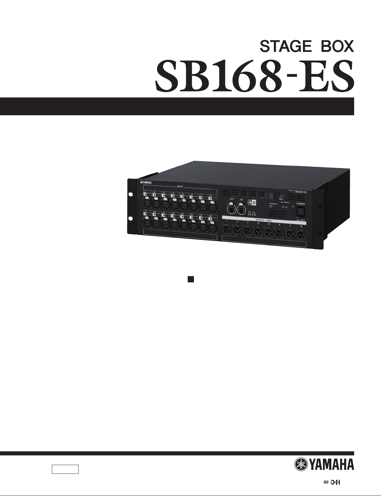
Yamaha SB-168-ES Service Manual
SERVICE MANUAL
SERVICE MANUAL
CONTENTS(目次)
SPECIFICATIONS(総合仕様) ........................................... 4
PANEL LAYOUT(パネルレイアウト) ................................ 6
DIMENSIONS(寸法図) ...................................................... 7
CIRCUITBOARDLAYOUT(ユニットレイアウト) ........... 8
DISASSEMBLYPROCEDURE(分解手順)..................... 10
LSIPINDESCRIPTION(LSI 端子機能表)....................... 19
ICBLOCKDIAGRAM(IC ブロック図)............................ 27
CIRCUIT BOARDS(シート基板図) ................................. 30
TESTPROGRAM(テストプログラム) ....................... 46/60
INSPECTIONS(検査) ................................................. 74/76
HOWTOBACKUPSB168-ESDATA
(本体データのバックアップ方法) ................................ 78/79
FIRMWAREUPDATE
(ファームウェアのアップデート) ................................ 80/85
ERRORMESSAGES(エラーメッセージ) ................. 90/91
WARNINGMESSAGES(ワーニングメッセージ) ........... 92
PARTS LIST
BLOCK DIAGRAM(ブロックダイアグラム)
WIRING(基板結線図)
CIRCUIT DIAGRAM(回路図)
PA
200901-
011934
オープンプライス
HAMAMATSU, JAPAN
Copyright (c) Yamaha Corporation. All rights reserved. PDF & ’09.01

SB168-ES
IMPORTANT NOTICE
This manual has been provided for the use of authorized Yamaha Retailers and their service personnel. It has been assumed that basic
service procedures inherent to the industry, and more specifically Yamaha Products, are already known and understood by the users,
and have therefore not been restated.
WARNING : Failure to follow appropriate service and safety procedures when servicing this product may result in personal injury,
IMPORTANT : This presentation or sale of this manual to any individual or firm does not constitute authorization certification,
The data provided is belived to be accurate and applicable to the unit(s) indicated on the cover. The research engineering, and service
departments of Yamaha are continually striving to improve Yamaha products. Modifications are, therefore, inevitable and changes in
specification are subject to change without notice or obligation to retrofit. Should any discrepancy appear to exist, please contact the
distributor’s Service Division.
WARNING : Static discharges can destroy expensive components. Discharge any static electricity your body may have accumulated
destruction of expensive components and failure of the product to perform as specified. For these reasons, we advise
all Yamaha product owners that all service required should be performed by an authorized Yamaha Retailer or the
appointed service representative.
recognition of any applicable technical capabilities, or establish a principal-agent relationship of any form.
by grounding yourself to the ground bus in the unit (heavy gauge black wires connect to this bus.)
IMPORTANT : Turn the unit OFF during disassembly and parts replacement. Recheck all work before you apply power to the unit.
WARNING: This product contains chemicals known to the State of California to cause cancer, or birth defects or other reproductive harm.
DO NOT PLACE SOLDER, ELECTRICAL/ELECTRONIC OR PLASTIC COMPONENTS IN YOUR MOUTH FOR ANY REASON WHAT SO EVER!
Avoid prolonged, unprotected contact between solder and your skin! When soldering, do not inhale solder fumes or expose eyes to solder/
flux vapor!
If you come in contact with solder or components located inside the enclosure of this product, wash your hands before handling food.
LITHIUM BATTERY HANDLING
This product uses a lithium battery for memory back-up.
WARNING :
Leave lithium battery replacement to qualifi ed service personnel.
Always replace with batteries of the same type.
When installing on the PC board by soldering, solder using the connection terminals provided on the battery cells.
Never solder directly to the cells. Perform the soldering as quickly as possible.
Never reverse the battery polarities when installing.
Do not short the batteries.
Do not attempt to recharge these batteries.
Do not disasemble the batteries.
Never heat batteries or throw them into fi re.
ADVARSEL!
Lithiumbatteri-Eksplosionsfare ved fejlagtig håndtering. Udskiftning må kun ske med batteri af samme fabrikat og type. levér det brugte batteri tilbage til
leverandren.
VARNING
Explosionsfara vid felaktigt batteribyte.
Använd samma batterityp eller en ekvivalent typ som rekommenderas av apparattillverkaren.
Kassera använt batteri enligt fabrikantens instruktion.
VAROITUS
Paristo voi räjähtää, jos se on virheellisesti asennettu.
Vaihda paristo ainoastaan laitevalmistajan suosittelemaan tyyppiiin.
Hävitä käytetty paristo valmistajan ohjeiden mukaisesti.
The following information complies with Dutch offi cial Gazette 1995. 45; ESSENTIALS OF ORDER ON THE COLLECTION OF BATTERIES.
• Please refer to the diassembly procedure for the removal of Back-up Battery.
• Leest u voor het verwijderen van de backup batterij deze beschrijving.
Lithium batteries are dangerous because they can be exploded by improper handling. Observe the following precautions when
handling or replacing lithium batteries.
2
リチウム電池の取り扱い
<注意>
リチウム電池を誤って交換すると爆発する危険があります。交換する場合は、サービスマニュアルで指定された部品を使用して
ください。
SB168-ES
IMPORTANT NOTICE FOR THE UNITED KINGDOM
Connecting the Plug and Cord
WARNING: THIS APPARATUS MUST BE EARTHED
IMPORTANT. The wires in this mains lead are coloured in accordance with the following code:
GREEN-AND-YELLOW : EARTH
BLUE : NEUTRAL
BROWN : LIVE
As the colours of the wires in the mains lead of this apparatus may not correspond with the coloured markings identifying the terminals
in your plug proceed as follows:
The wire which is coloured GREEN-and-YELLOW must be connected to the terminal in the plug which is marked by the letter E or by
the safety earth symbol or colored GREEN or GREEN-and-YELLOW.
The wire which is coloured BLUE must be connected to the terminal which is marked with the letter N or coloured BLACK.
The wire which is coloured BROWN must be connected to the terminal which is marked with the letter L or coloured RED.
• This applies only to products distributed by Yamaha Music U.K. Ltd. (3 wires)
WARNING
Components having special characteristics are marked and must be replaced with parts having specifi cation equal to those
originally installed.
印の部品は、安全を維持するために重要な部品です。交換する場合は、安全のために必ず指定の部品をご使用ください。
3
SB168-ES
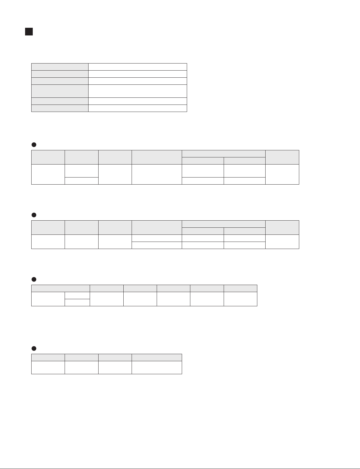
SPECIFICATIONS(総合仕様)
General Specification(一般仕様)
Power Requirements 65 W
Dimensions 480 x 350 x 132 mm (W x D x H)
Net Weight 8 kg
Temperature Range
AC Cable Length 250 cm
Accessories Owner’s Manual, AC Cable
Input/Output Characteristics(入出力特性)
Analog Input Characteristics
Input
Terminals
INPUT 1–16
*1. XLR-3-31 type connectors are balanced. (1=GND, 2=HOT, 3=COLD)
* In these specifications, when dBu represents a specific voltage, 0 dBu is referenced to 0.775 Vrms.
* AD converters are 24-bit linear, 128-times oversampling.
Operation free-air : ±0 °C to +40 °C
Storage : -20 °C to +60 °C
GAIN
-62 dB
Actual Load
Impedance
3 kΩ
For Use With Nominal
50–600 Ω Mics &
600 Ω Lines
Nominal Max. before clip
-62 dBu
(0.616 mV)
Input Level
-42 dBu (6.16 mV)
+30 dBu (24.5 V)+10 dBu (2.45 V)+10dB
Connector
XLR-3-31 type
(Balanced)*
1
Analog Output Characteristics
Output
Terminals
OUTPUT 1–8 75 Ω 600 Ω Lines
*1. XLR-3-32 type connectors are balanced. (1=GND, 2=HOT, 3=COLD)
* In these specifications, when dBu represents a specific voltage, 0 dBu is referenced to 0.775 Vrms.
* DA converters are 24-bit, 128-times oversampling.
Actual Source
Impedance
For Use With
Nominal
Max. Output Level
Select SW
+24 dB (default) +4 dBu (1.23 V) +24 dBu (12.3 V)
+18 dB -2 dBu (616 mV) +18 dBu (6.16 V)
Output Level
Nominal Max. before clip
Connector
XLR-3-32 type
(Balanced)*
1
Digital Input/Output Characteristics
Terminal Format Data Length Level Audio Connector
EtherSound
*1. Use a RJ-45 connector compliant with Neutrik EtherCon
* Use a CAT5e STP (Shielded Twisted Pair) cable compliant with EtherSound.
* Use electrically conductive tape to securely connect the metal part of the connector with the shielded part of the cable in order to prevent
electromagnetic interference.
* An EtherSound certified cable is recommended. Maximum length available depends on each cable specification.
IN
OUT
EtherSound 24bit 100 Base-TX
®
8 ch Input/
16 ch Output
RJ-45*
1
Control I/O Characteristics
Terminal Format Level Connector
NETWORK IEE802.3
* A CAT5e STP (Shielded Twisted Pair) cable is recommended. Maximum length is 100 m.
10 Base-T/
100 Base-TX
RJ-45
4
Electrical Characteristics(電気的特性)
Output impedance of single generator: 150 Ω
Measured with another SB168-ES through EtherSound
Frequency Response Fs= 44.1 kHz or 48 kHz@20 Hz–20 kHz, reference to the nominal output level @ 1 kHz
Input Output RL Conditions Min. Typ. Max. Unit
INPUT 1–16 OUTPUT 1–8 600 Ω GAIN: +10dB -1.5 0 0.5 dB
Gain Error Fs= 44.1 kHz, 48 kHz@ 1 kHz
Input Output RL Conditions Min. Typ. Max. Unit
Input level: -62 dBu, GAIN: -62dB →
INPUT 1–16 OUTPUT 1–8 600 Ω
Output level +4.0 dBu (Typ.)
Input level: +10 dBu, GAIN: +10dB →
Output level +4.0 dBu (Typ.)
Total Harmonic Distortion Fs= 44.1 kHz or 48 kHz
Input Output RL Conditions Min. Typ. Max. Unit
INPUT 1–16 OUTPUT 1–8 600 Ω
* Total Harmonic Distortion is measured with a 18 dB/octave filter @80 kHz.
-2 0 2
-2 0 2
0.1+4 dBu@20 Hz 20 kHz, GAIN: -62dB
0.05+4 dBu@20 Hz 20 kHz, GAIN: -10dB
SB168-ES
dB
%
Hum & Noise Fs= 44.1 kHz or 48 kHz, EIN= Equivalent Input Noise
Input Output RL Conditions Min. Typ. Max. Unit
-128
INPUT 1–16 OUTPUT 1–8 600 Ω
* Hum & Noise are measured with a 6 dB/octave filter @12.7 kHz; equivalent to a 20 kHz filter with infinite dB/octave attenuation.
Rs=150 Ω, GAIN: -62 dB
Rs=150 Ω, GAIN: -10 dB -80-84
EIN
-62
Dynamic Range Fs= 44.1 kHz or 48 kHz
Input Output RL Conditions Min. Typ. Max. Unit
INPUT 1–16 OUTPUT 1–8 600 Ω dB108GAIN: +10 dB
* Dynamic Range is measured with a 6 dB/octave filter @12.7 kHz; equivalent to a 20 kHz filter with infinite dB/octave attenuation.
Crosstalk @ 1 kHz Fs= 44.1 kHz or 48 kHz
From/To To/From Conditions Min. Typ. Max. Unit
INPUT N INPUT (N-1) or (N+1)
INPUT 1–16, adjacent inputs,
GAIN: +10dB
-80
-80OUTPUT 1–8, input to outputOUTPUT (N-1) or (N+1)OUTPUT N
Phantom Voltage
Output Conditions Min. Typ. Max. Unit
dBu
dB
V504846hot & cold: No loadINPUT 1–16
Sampling Frequency
Parameter Conditions Min. Typ. Max. Unit
Internal Clock
Frequency 48 kHz
Accuracy 50 ppm
kHz49.2043.00Frequency RangeExternal Clock
5
SB168-ES
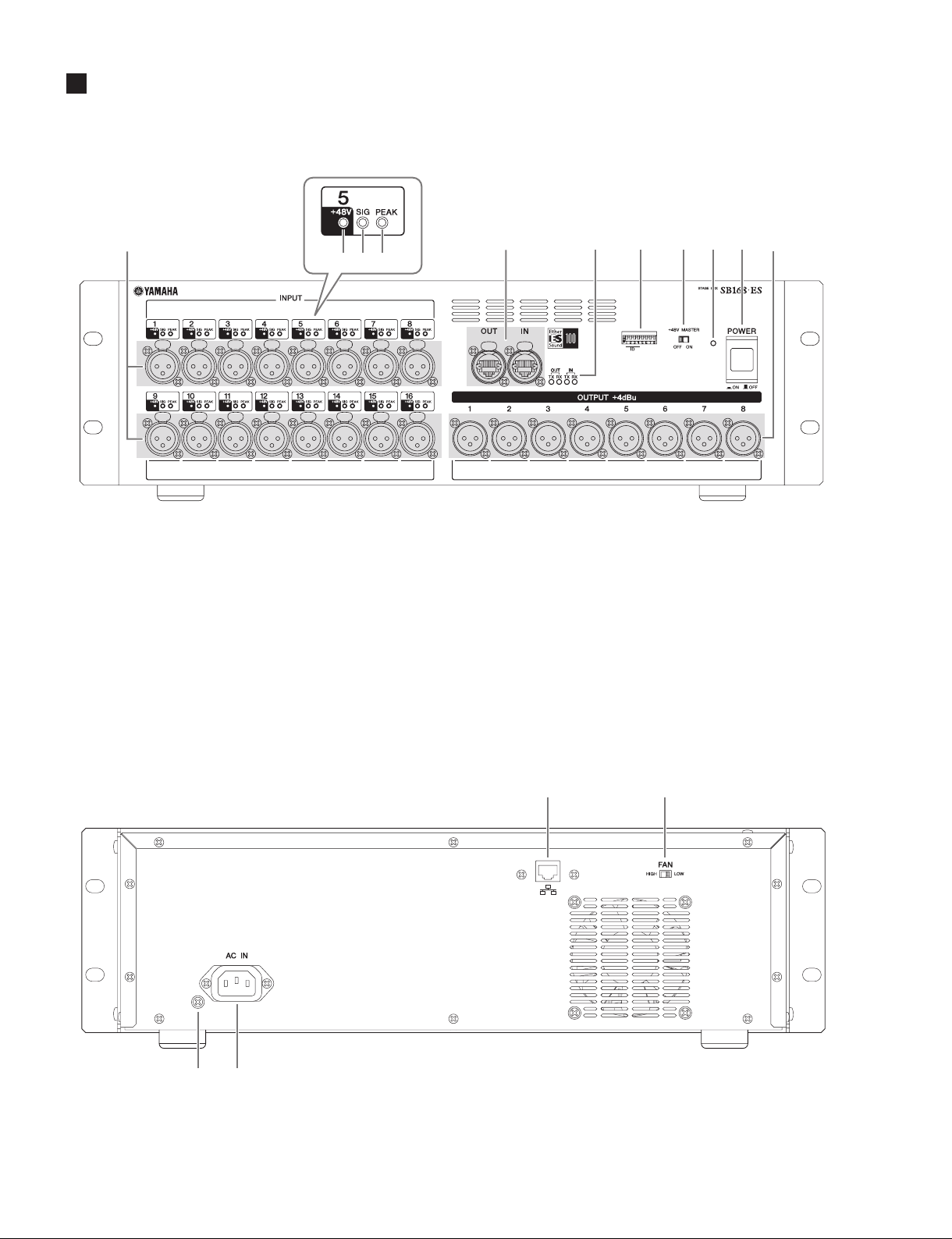
PANEL LAYOUT(パネルレイアウト)
• Front Panel(フロントパネル)
/
q [INPUT 1–16] Connectors
w [+48V] Indicators
e [SIG] Indicators
r [PEAK] Indicators
t EtherSound [IN]/[OUT] Connectors
y IN/OUT [TX]/[RX] Indicators
u DIP Switches [1–8]
i [+48V MASTER] Switch
o Power Indicator
!0 [POWER] Switch
!1 OUTPUT [1–8] Connectors
4)0
1
q [INPUT(インプット)1 〜 16]端子
w [+48V]インジケーター
e [SIG(シグナル)]インジケーター
r [PEAK(ピーク)]インジケーター
t EtherSound[IN]/[OUT]端子
y IN/OUT[TX]/[RX]インジケーター
u ディップスイッチ[1 〜 8]
i [+48VMASTER](+48Vマスター )スイッチ
o 電源インジケーター
!0 [POWER]スイッチ
!1 OUTPUT(アウトプット)[1 〜 8]端子
2 * - 6
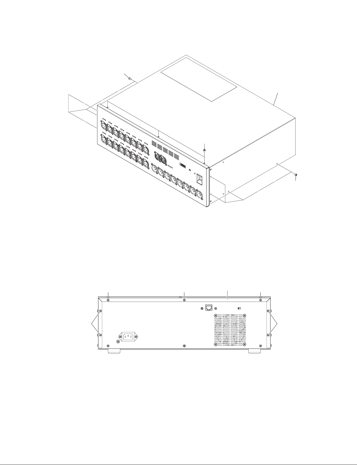
• Rear Panel(リアパネル)
/ 4
q Earth Screw
w [AC IN] Socket
e NETWORK Connector
r [FAN] Switch
6
) 0
q アース用ネジ
q [ACIN]端子
q NETWORK端子
q [FAN]スイッチ
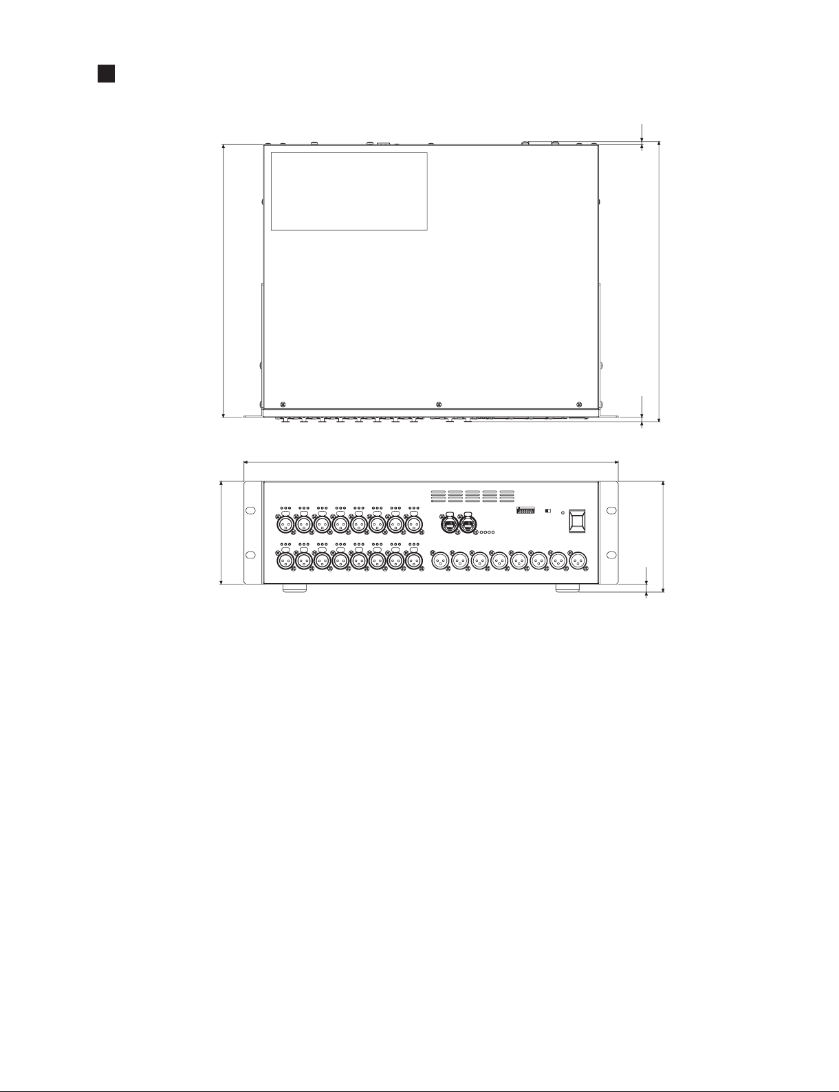
DIMENSIONS(寸法図)
SB168-ES
(4)
350
132
359.7
5.7
480
142
10
Unit(単位): mm
7
SB168-ES
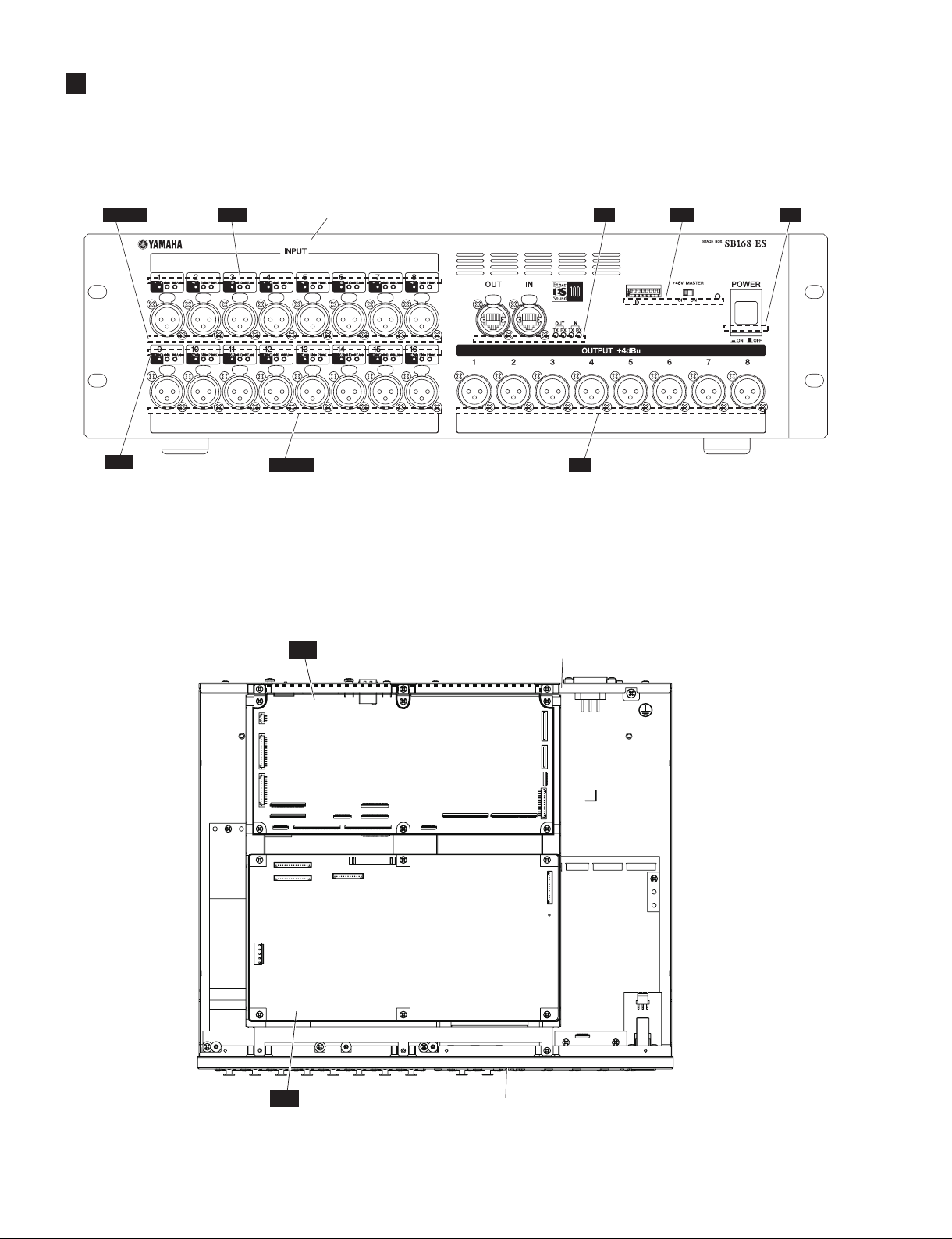
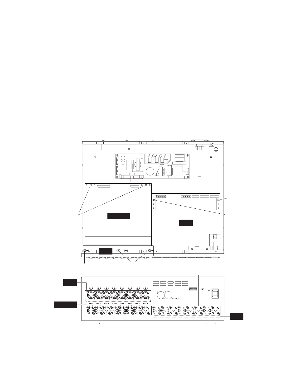
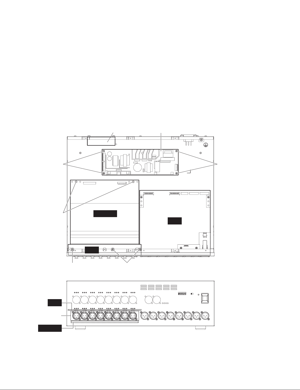
CIRCUIT BOARD LAYOUT(ユニットレイアウト)
• Front View(前面から見た図)
FRONT PANEL
HAAD2
(ch 1-8)
LD1
(フロントパネル)
ES
SW
PS
LD2
(ch 9-16)
• Top View <Upper section> (上面から見た図〈上段〉)
DM
DAHAAD2
REAR PANEL
(リアパネル印刷品)
DC
FRONT PANEL
(フロントパネル)
8
SB168-ES
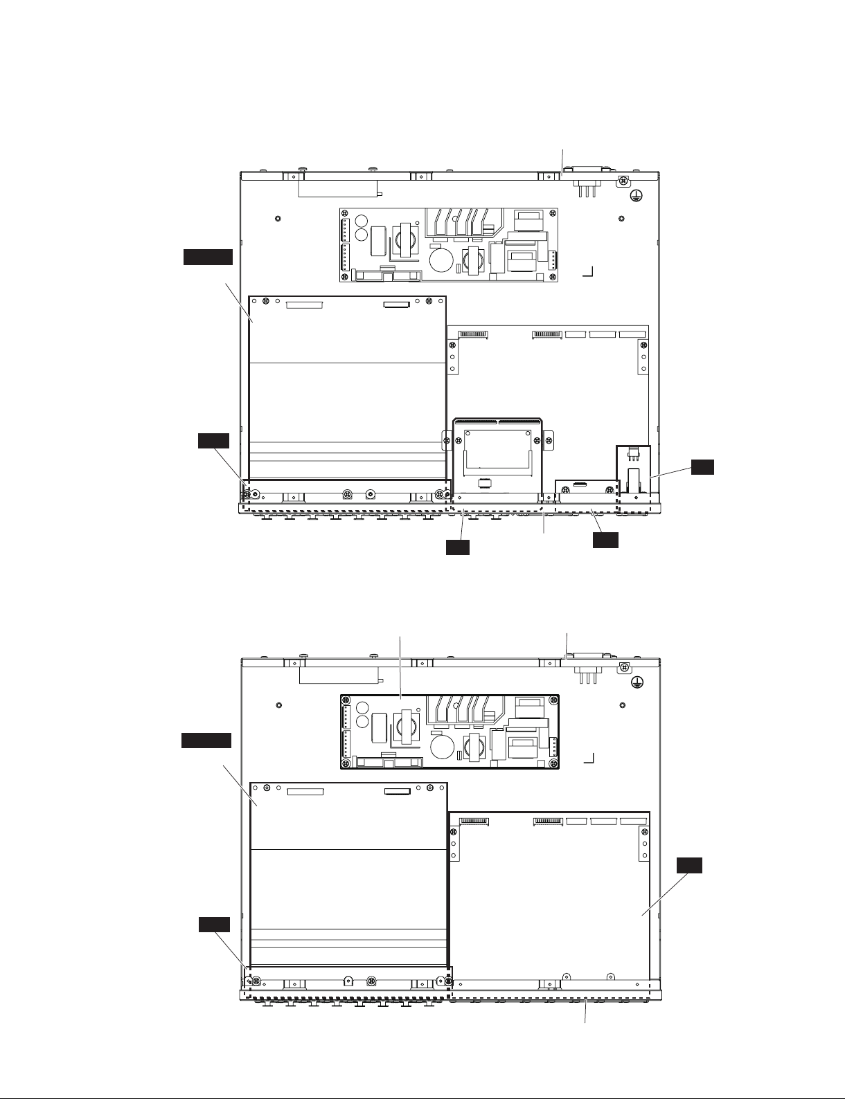
• Top View <Middle section> (上面から見た図〈中段〉)
HAAD2
(CH1-8)
LD1
REAR PANEL
(リアパネル印刷品)
PS
• Top View <Lower section> (上面から見た図〈下段〉)
POWER SUPPLY UNIT
(電源ユニット)
HAAD2
(CH9-16)
LD2
ES
FRONT PANEL
(フロントパネル)
(リアパネル印刷品)
SW
REAR PANEL
DA
FRONT PANEL
(フロントパネル)
9
SB168-ES
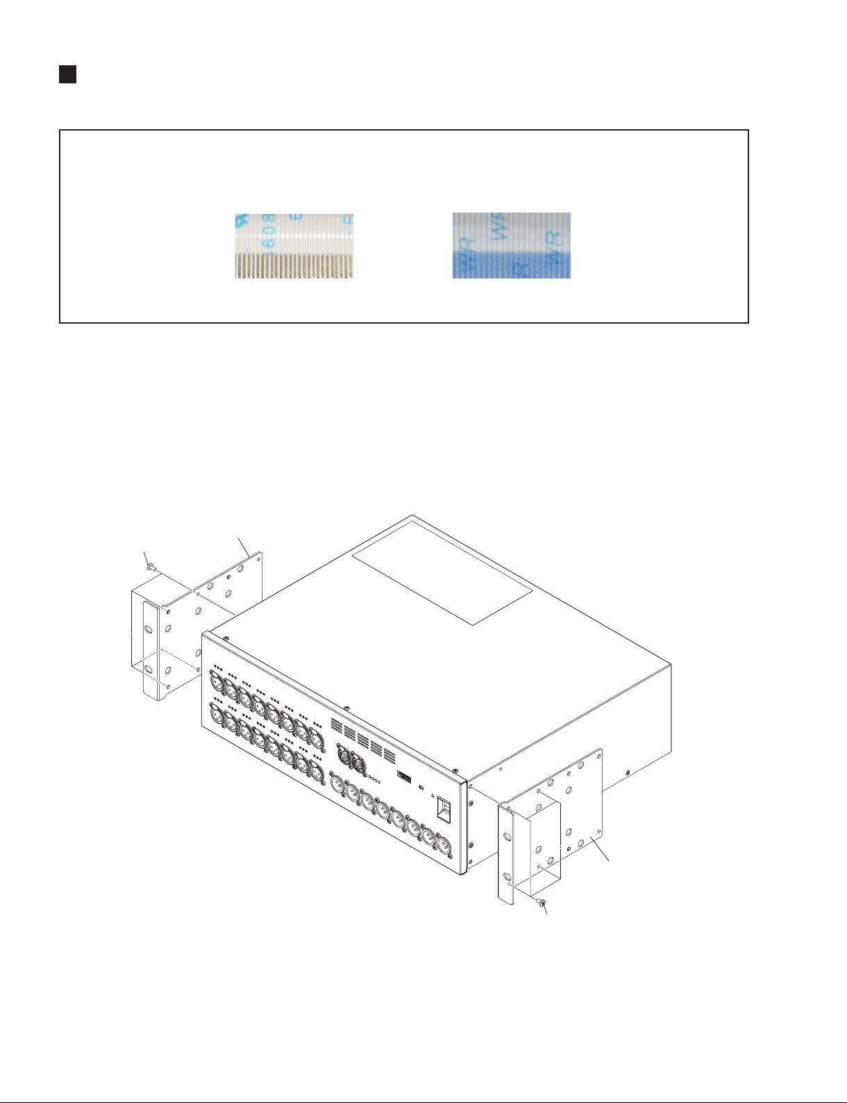
DISASSEMBLY PROCEDURE(分解手順)
Precautions
* Notes on Flat Cable
Contacts are visible from the back. Pay attention not to
insert and install the cable to the connector inversely.
(Photo 1)
1. Top Cover
(注意事項)
Front Side
(Time required: About 4 minutes)
(表面)
Photo 1
1-1 Remove the eight (8) screws marked [1160]. The right
and left rack angle can then be removed. (Fig. 1)
1-2 Remove the eighteen (18) screws marked [1110]. The
top cover can then be removed. (Fig. 2, Fig. 3)
RACK ANGLE
(ラックアングル)
[1160]
※ フラットケーブルの注意
接点が裏面から透けて見えます。コネクタにケーブルの
表・裏を逆に差込まないように注意して取り付けてくだ
さい。(写真 1)
Back Side
(写真 1)
1. トップカバー
(裏面)
(所要時間:約 4 分)
1-1 [1160] のネジ 8 本を外して、左右のラックアング
ルを外します。(図 1)
1-2 [1110] のネジ 18 本を外して、トップカバーを外
します。(図 2、図 3)
10
RACK ANGLE
(ラックアングル)
[1160]
[1160]:BINDHEADSCREW4X8(小ネジ+BIND)4.0X8MFZN2B3IT(WE99710R)
Fig. 1
(図 1)
[1110]
SB168-ES
TOP COVER
(トップカバー)
[111 0]
[111 0]
[1110]:BINDHEADTAPPINGSCREW-S(Sタイト+BIND)3.0X6MFZN2B3(WE87780R)
Fig. 2
(図 2)
• Back view
[1110] [111 0] [ 1110]
[1110]
[1110]:BINDHEADTAPPINGSCREW-S(Sタイト+BIND)3.0X6MFZN2B3(WE87780R)
Fig. 3
(図 3)
TOP COVER
(トップカバー)
[111 0]
11
SB168-ES
2. DM Circuit Board
(Time required: About 6 minutes)
2-1 Remove the top cover. (See procedure 1.)
2-2 Remove the two (2) screws marked [970] and six (6)
screws marked [980]. The DM circuit board can then
be removed. (Fig. 4)
• Back view
AC INLET ASSEMBLY
(インレットAssy)
• LITHIUM BATTERY(リチウム電池)
Battery VN103500
VN103600(Battery holder for VN103500)
Notice for back-up battery removal
Push the battery as shown in figure,
then the battery will pop up.
Druk de batterij naar beneden zoals
aangeven in de tekening de batterij
springt dan naar voren.
Battery
Battery holder
2. DM シート
(所要時間:約 6 分)
2-1 トップカバーを外します。(1 項参照)
2-2 [970] の ネ ジ 2 本 と [980] の ネ ジ 6 本を外して、
DM シートを外します。(図 4)
[970][640]
DM
AC INLET ASSEMBLY
(インレットAssy)
[650]
12
• Top view
[980]
[910]
[640]:BINDHEADB-TIGHTSCREW(Bタイト+BIND)3.0X8MFZN2B3 (WE774400)
[650]:BINDHEADTAPPINGSCREW-S(Sタイト+BIND)4.0X8MFZN2B3(WE99480R)
[910]:BINDHEADTAPPINGSCREW-S(Sタイト+BIND)3.0X6MFZN2B3(WE87780R)
[970]:BINDHEADTAPPINGSCREW-S(Sタイト+BIND)3.0X6MFZN2B3(WE87780R)
[980]:BINDHEADTAPPINGSCREW-S(Sタイト+BIND)3.0X6MFZN2B3(WE87780R)
DM
DC
Fig. 4
(図 4)
[980]
[910]

SB168-ES
3. Replacing the Lithium Battery
(Time required: About 6 minutes)
3-1 Remove the top cover. (See procedure 1.)
3-2 Replace the lithium battery on the DM circuit board.
(Fig. 4)
* The lithium battery is not part of the DM circuit
board. When replacing the DM circuit board, remove
the lithium battery from the circuit board and install
it on the new circuit board. (Fig. 4)
* Refer to the section “HOW TO BACKUP SB168-ES
DATA” before replacing the lithium battery. (See
page 78)
4. DC Circuit Board
(Time required: About 5 minutes)
4-1 Remove the top cover. (See procedure 1.)
4-2 Remove the six (6) screws marked [910]. The DC
circuit board can then be removed. (Fig. 4)
5. ES Circuit Board
(Time required: About 6 minutes)
5-1 Remove the top cover. (See procedure 1.)
5-2 Remove the DC circuit board. (See procedure 4.)
5-3 Remove the two (2) screws marked [820] and four (4)
screws marked [830]. The ES circuit board can then be
removed. (Fig. 5)
3. リチウム電池の交換
3-1 トップカバーを外します。(1 項参照)
3-2 DM シート上より、リチウム電池を交換すること
ができます。(図 4)
※ リチウム電池は、DM シートの構成部品ではありません。
DM シートを交換する際には、本体のシートからリチウ
ム電池を取り外して、新しいシートに取り付けてくださ
い。(図 4)
※ リチウム電池の交換を行うときは、「本体データのバッ
クアップ方法」の項を参照してください。(79 ページ参
照)
4. DC シート
4-1 トップカバーを外します。(1 項参照)
4-2 [910] のネジ 6 本を外して、DC シートを外します。
(図 4)
5. ES シート
5-1 トップカバーを外します。(1 項参照)
5-2 DC シートを外します。(4 項参照)
5-3 [820] の ネ ジ 2 本 と [830] の ネ ジ 4 本 を 外 し て、
ES シートを外します。(図 5)
(所要時間:約 5 分)
(所要時間:約 6 分)
(所要時間:約 6 分)
6. SW Circuit Board
(Time required: About 5 minutes)
6-1 Remove the top cover. (See procedure 1.)
6-2 Remove the two (2) screws marked [200]. The SW
circuit board can then be removed. (Fig. 5)
7. PS Circuit Board
(Time required: About 5 minutes)
7-1 Remove the top cover. (See procedure 1.)
7-2 Remove the two (2) screws marked [160]. (Fig. 5)
7-3 Pull the PS circuit board toward the rear side to remove
it. (Fig. 5)
The PS circuit board and the power switch knob will be
separated then.
8. AC Inlet Assembly
(Time required: About 5 minutes)
8-1 Remove the top cover. (See procedure 1.)
8-2 Remove the two (2) screws marked [640] and the screw
marked [650]. The AC inlet assembly can then be
removed. (Fig. 4)
6. SW シート
6-1 トップカバーを外します。(1 項参照)
6-2 [200] のネジ 2 本を外して、SW シートを外します。
(図 5)
7. PS シート
7-1 トップカバーを外します。(1 項参照)
7-2 [160] のネジ 2 本を外します。(図 5)
7-3 PS シートをリア側に引くように外します。(図 5)
このとき PS シートと PSW ノブが分離します。
8. インレット Assy
8-1 トップカバーを外します。(1 項参照)
8-2 [640] のネジ 2 本と [650] のネジ 1 本を外して、イ
ンレット Assy を外します。(図 4)
(所要時間:約 5 分)
(所要時間:約 5 分)
(所要時間:約 5 分)
13
SB168-ES
9. Sheet Support
(Time required: About 9 minutes)
9-1 Remove the top cover. (See procedure 1.)
9-2 Remove the DM circuit board. (See procedure 2.)
9-3 Remove the DC circuit board. (See procedure 4.)
9-4 Remove the ES circuit board. (See procedure 5.)
9-5 Remove the six (6) screws marked [760]. The sheet
support can then be removed. (Fig. 5)
• Top view
[760] [760]
9. シートサポート
9-1 トップカバーを外します。(1 項参照)
9-2 DM シートを外します。(2 項参照)
9-3 DC シートを外します。(4 項参照)
9-4 ES シートを外します。(5 項参照)
9-5 [760] のネジ 6 本を外して、シートサポートを外
します。(図 5)
(所要時間:約 9 分)
[820]
SHEET SUPPORT
(シートサポート)
• Front view
ES
ES
[200][760][760][760]
SW PS
[830]
SW
[160]
PS
POWER SWITCH KNOB
(PSWノブ)
PS
14
[160]:BINDHEADTAPPINGSCREW-S(Sタイト+BIND)3.0X6MFZN2B3(WE87780R)
[200]:BINDHEADTAPPINGSCREW-S(Sタイト+BIND)3.0X6MFZN2B3(WE87780R)
[760]:BINDHEADTAPPINGSCREW-S(Sタイト+BIND)3.0X6MFZN2B3(WE87780R)
[820]:BINDHEADTAPPINGSCREW-S(Sタイト+BIND)3.0X6MFZN2B3(WE87780R)
[830]:SCREWTP#B+BOND(Bタイト+BOND)3.0X8MFZN2B3(WE774100)
Fig. 5
(図 5)
SB168-ES
10. DA Circuit Board
(Time required: About 12 minutes)
10-1 Remove the sheet support. (See procedure 9.)
10-2 Remove the sixteen (16) screws marked [510], two
(2) screws marked [520] and two (2) spacer hexagon
marked [570]. The DA circuit board can then be
removed. (Fig. 6)
11. HAAD2 Circuit Board (ch 1 – ch 8)
(Time required: About 12 minutes)
11-1 Remove the sheet support. (See procedure 9.)
11-2 Remove the sixteen (16) screws marked [410] and two
(2) screws marked [420]. The HAAD2 circuit board
(ch 1 – ch 8) can then be removed. (Fig. 6)
• Top view
10. DA シート
10-1 シートサポートを外します。(9 項参照)
10-2 [510] のネジ 16 本と [520] のネジ 2 本、[570] の六
角スペーサー 2 本を外して、DA シートを外します。
(図 6)
(所要時間:約 12 分)
11. HAAD2 シート(ch1‒ch8)
(所要時間:約 12 分)
11-1 シートサポートを外します。(9 項参照)
11-2 [410] のネジ 16 本と [420] のネジ 2 本 を外し て、
HAAD2 シート(ch1‒ch8)を外します。(図 6)
[420]
LD1
[410]
HAAD2
(ch 1 – ch 8)
[410]:SCREWTP#B+BOND(Bタイト+BOND)3.0X8MFZN2B3(WE774100)
[420]:BINDHEADTAPPINGSCREW-S(Sタイト+BIND)3.0X6MFZN2B3(WE87780R)
[470]:BINDHEADTAPPINGSCREW-S(Sタイト+BIND)3.0X6MFZN2B3(WE87780R)
[510]:SCREWTP#B+BOND(Bタイト+BOND)3.0X8MFZN2B3(WE774100)
[520]:BINDHEADTAPPINGSCREW-S(Sタイト+BIND)3.0X6MFZN2B3(WE87780R)
[570]:SPACERHEXAGON(六角スペーサーM3)L=45(WP898900)
LD1
• Front view
HAAD2
(ch 1 – ch 8)
[520], [570]
[520]
DA
[470][470]
[510]
DA
Fig. 6
(図 6)
15
SB168-ES
12. HAAD2 Circuit Board (ch 9 – ch 16)
(Time required: About 15 minutes)
12-1 Remove the sheet support. (See procedure 9.)
12-2 Remove the HAAD2 circuit board (ch 1 – ch 8).
(See procedure 11.)
12-3 Remove the sixteen (16) screws marked [310] and two
(2) spacer hexagon marked [320]. The HAAD2 circuit
board (ch 9 – ch 16) can then be removed. (Fig. 7)
• Top view
[70] [70]
DC FAN MOTOR
(DCファンモーター)
12. HAAD2 シート(ch9‒ch16)
(所要時間:約 15 分)
12-1 シートサポートを外します。(9 項参照)
12-2 HAAD2 シート(ch1‒ch8)を外します。
(11 項参照)
12-3 [310] のネジ 16 本と [320] の六角スペーサー 2 本
を外して、HAAD2 シート(ch9 ‒ ch 16)を外し
ます。(図 7)
POWER SUPPLY UNIT
(電源ユニット)
[320]
LD2
[310]
HAAD2
(ch 9 – ch 16)
HAAD2
(ch 9 – ch 16)
DA
LD2
[370][370]
• Front view
[70]: BINDHEADTAPPINGSCREW-S(Sタイト+BIND)3.0X6MFZN2W3(WH673900)
[310]:SCREWTP#B+BOND(Bタイト+BOND)3.0X8MFZN2B3(WE774100)
[320]:SPACERHEXAGON(六角スペーサーM3)L=45(WP898900)
[370]:BINDHEADTAPPINGSCREW-S(Sタイト+BIND)3.0X6MFZN2B3(WE87780R)
Fig. 7
(図 7)
DA
16
SB168-ES
13. LD1 Circuit Board, LD2 Circuit Board, LED Lens
* Installation position can be reversed and there is no
problem if the positions of the LD1 circuit board and
the LD2 circuit board are opposite.
This document describes an example that the LD1
circuit board is installed over the LD2 circuit board.
13-1 Remove the sheet support. (See procedure 9.)
13-2 LD1 Circuit Board, LED Lens (ch 1 – ch 8)
(Time required: About 9 minutes)
13-2-1 Remove the three (3) screws marked [470]. The LD1
circuit board can then be removed. (Fig. 6)
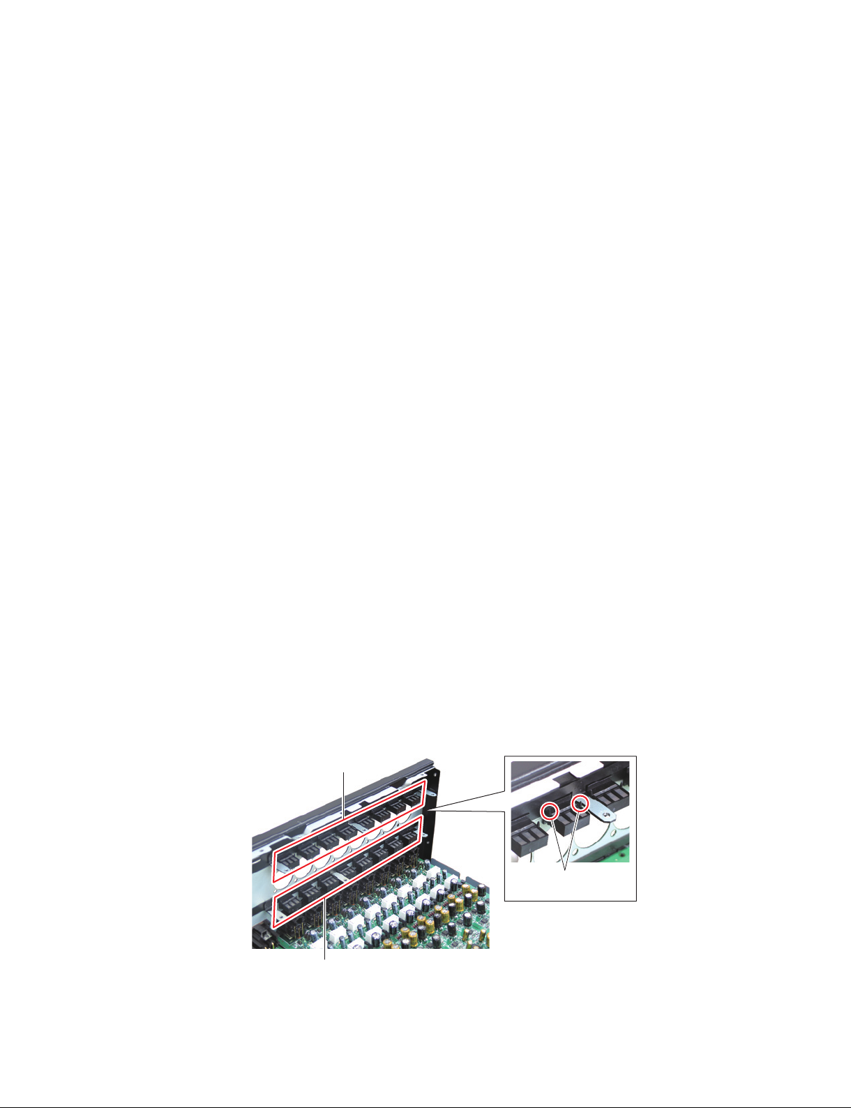
13-2-2 Remove the LED lens (ch 1 – ch 8). (Photo 2)
13-3 LD2 Circuit Board, LED Lens (ch 9 – ch 16)
(Time required: About 12 minutes)
13-3-1 Remove the HAAD2 circuit board (ch 1 – ch 8).
(See procedure 11.)
13-3-2 Remove the three (3) screws marked [370]. The LD2
circuit board can then be removed. (Fig. 7)
13-3-3 Remove the LED lens (ch 9 – ch 16). (Photo 2)
* When installing the LD1 circuit board and LD2 circuit
board, install with the boss of the LED lens inserted
into the hole of the circuit boards. (Photo 2)
13. LD1 シート、LD2 シート、LED レンズ
※ LD1 シートと LD2 シートの取り付け位置が逆でも問題
ありません。
ここでは LD1 シートが上にあるとして、説明します。
13-1 シートサポートを外します。(9 項参照)
13-2 LD1 シート、LED レンズ(ch 1‒ch 8)
(所要時間:約 9 分)
13-2-1 [470] のネジ 3 本を外して、LD1 シートを外します。
(図 6)
ch
ch
ch
1‒
8)を外します。(写真 2)
ch
ch
1‒
8)を外します。
ch
9‒
16)を外します。(写真 2)
13-2-2 LED レンズ(
13-3 LD2 シート、LED レンズ(ch 9‒ch 16)
(所要時間:約 12 分)
13-3-1 HAAD2 シート(
(11 項参照)
13-3-2 [370] のネジ 3 本を外して、LD2 シートを外します。
(図 7)
13-3-3 LED レンズ(
※ LD1 シートと LD2 シートを取り付ける時は、LED レン
ズのボスがシートの穴にはまるように取り付けてくださ
い。(写真 2)
14. Power Supply Unit
(Time required: About 9 minutes)
14-1 Remove the sheet support. (See procedure 9.)
14-2 Remove the four (4) screws marked [70]. The power
supply unit can then be removed. (Fig. 7)
LED LENS (ch 1 – ch 8)
(LEDレンズ)
14. 電源ユニット
(所要時間:約 9 分)
14-1 シートサポートを外します。(9 項参照)
14-2 [70] のネジ 4 本を外して、電源ユニットを外しま
す。(図 7)
Angular portion
(角部)
LED LENS (ch 9 – ch 16)
(LEDレンズ)
Photo 2
(写真 2)
17
SB168-ES
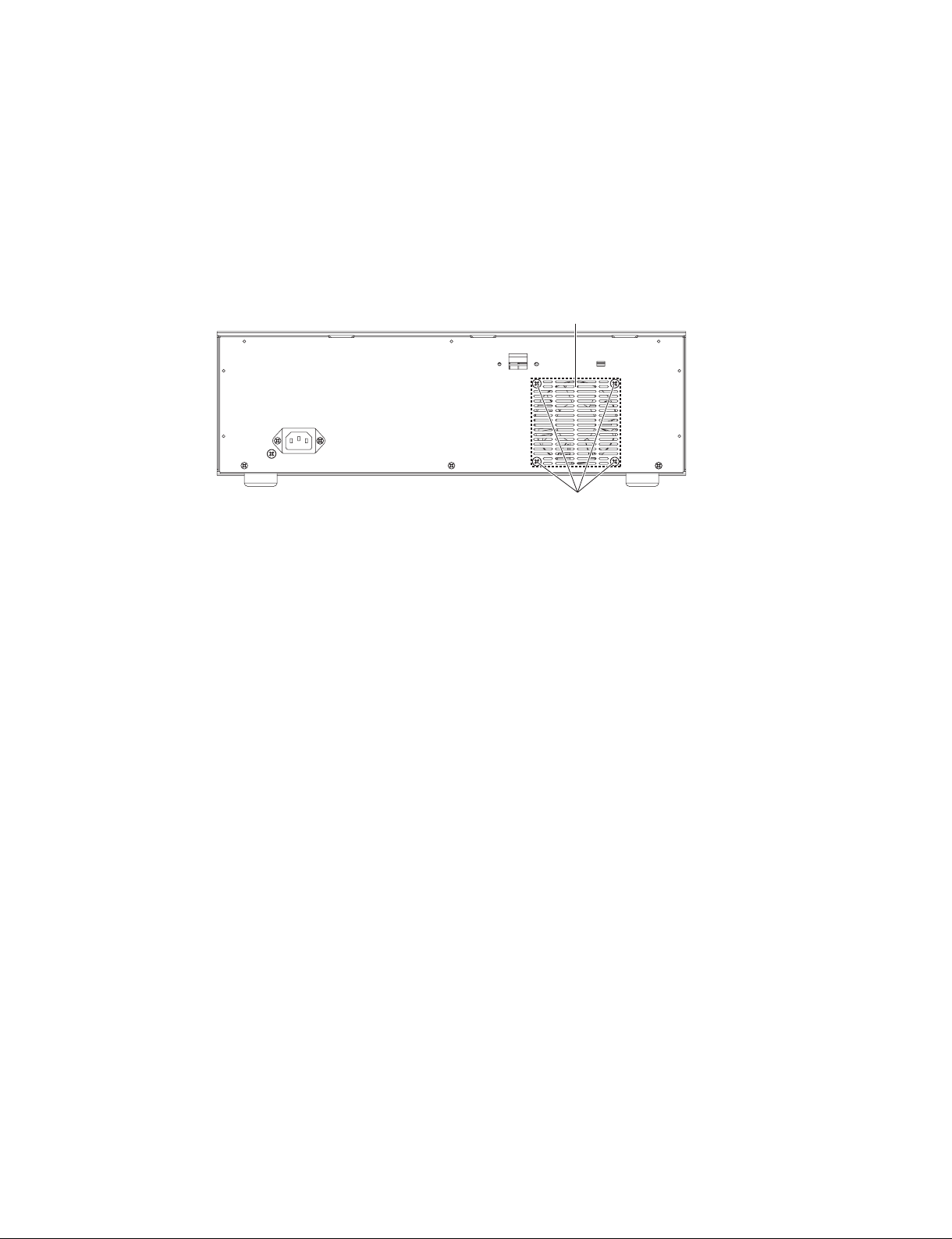
15. DC Fan Motor
(Time required: About 9 minutes)
15-1 Remove the sheet support. (See procedure 9.)
15-2 Remove the four (4) screws marked [700]. The DC fan
motor can then be removed. (Fig. 7, Fig. 8)
• Back view
[700]:BINDHEADSCREW(小ネジ+BIND)4.0X35MFZN2B3SP(WE99920R)
Fig. 8
15. DC ファンモーター
15-1 シートサポートを外します。(9 項参照)
15-2 [700] のネジ 4 本を外して、DC ファンモーターを
外します。(図 7、図 8)
DC FAN MOTOR
(DCファンモーター)
[700]
(図 8)
(所要時間:約 9 分)
18
LSI PIN DESCRIPTION
SB168-ES
(LSI 端子機能表)
AK4393VF-E2
AK5385BVF-E2
DM9000AEP
(XW029A0R)
(X5364B00)
(X7029A00)
LC4064V-75TN100C
M38034M4H-225HP
R8A02032BG
RD-0759
S1L51252F32S200
YM3436D-VZ
YSS919C-FZ
(X8810A00)
(X7792A00)
(X3775A0R)
(XG948F00)
(XZ693C00)
(X8955A00)
(X6984A0R)
DC-DC MODULE
DAC
(Digital to Analog Converter) .........................................................26
ADC
(Analog to Digital Converter) ........................................................26
LAN CONTROLLER
CPU
CPLD
CPU
(SWX02) ...................................................................................... 20/21
(Complex Programmable Logic Device) ............................. 22
(EC-EXP) .............................................................................19
.............................................................................................26
DIR2
DSP7
PLLP2
(Digital Format Interface Receiver) .................................................25
(Digital Signal Processor) ............................................................... 23
(Gate Array) .........................................................................24
.................................................................................. 25
M38034M4H-225HP (X6984A0R) CPU (EC-EXP)
PIN
NO.
1
P62/AN2
2
P61/AN1
3
P60/AN0
4
P57/INT3
5
P56/PWM
6
P55/CNTR1
7
P54/CNTR0
8
P53/SRDY2
9
P52/SCLK2
P51/SOUT2
10
P50/SIN2
11
P47/SRDY1/CNTR2
12
P46/SCLK1
13
P45/TXD1
14
P44/RXD1
15
P43/INT2
16
P42/INT1
17
CNVSS
18
RESET
19
P41/INT00/XCIN
20
P40/INT40/XCOUT
21
22
XOUT
23
VSS
24
P27/(LED7)
25
P26/(LED6)
26
P25/(LED5)
27
P24/(LED4)
28
P23/(LED3)
29
P22/(LED2)
30
P21/(LED1)
31
P20/(LED0)
32
XIN
I/O FUNCTIONNAME
I/O
I/O
I/O
I/O
I/O
I/O
I/O
I/O
I/O
I/O
I/O
I/O
I/O
I/O
I/O
I/O
I/O
–
I/O
I/O
O
–
I/O
I/O
I/O
I/O
I/O
I/O
I/O
I/O
Port 6 / Analog input
Port 5/ Interrupt input
Port 5 / PWM output
Port 5 / Timer Y function
Port 5 / Timer X function
Port 5 / Serial I/O2 function
Port 4 / Serial I/O1 / timer Z function
Port 4 / Serial I/O1 function
Port 4 / Interrupt input
I
I
Reset
Port 4/ Interrupt input / Sub-clock generating I/O
Clock in
Clock out
Ground
Port 2
PIN
NO.
33
34
35
36
37
38
39
40
41
42
43
44
45
46
47
48
49
50
51
52
53
54
55
56
57
58
59
60
61
62
63
64
P17
P16
P15
P14
P13
P12
P11/INT01
P10/INT41
P07/AN15
P06/AN14
P05/AN13
P04/AN12
P03/AN11
P02/AN10
P01/AN9
P00/AN8
P37/SRDY3
P36/SCLK3
P35/TXD3
P34/TXR3
P33
P32
P31/DA2
P30/DA1
VCC
VREF
AVSS
P67/AN7
P66/AN6
P65/AN5
P64/AN4
P63/AN3
I/O FUNCTIONNAME
I/O
I/O
I/O
I/O
I/O
I/O
I/O
I/O
I/O
I/O
I/O
I/O
I/O
I/O
I/O
I/O
I/O
I/O
I/O
I/O
I/O
I/O
I/O
I/O
I/O
I/O
I/O
I/O
I/O
HAAD2: IC903
Port 1
Port 1 / Interrupt input
Port 0 / A/D converter output
Port 3 / Serial I/O3 function
Port 3
Port 3 / D/A converter output
–
–
–
Power supply +5 V
Power supply +5 V
Analog ground
Port 6 / A/D converter output
19
SB168-ES
R8A02032BG (X8810A00) CPU (SWX02)
PIN
NO.
OUTER
NAME
NO.
1
2
3
4
5
6
7
8
9
10
11
12
13
14
15
16
17
18
19
20
21
22
23
24
25
26
27
28
29
30
31
32
33
34
35
36
37
38
39
40
41
42
43
44
45
46
47
48
49
50
51
52
53
54
55
56
57
58
59
60
61
62
63
64
65
66
67
68
69
70
71
72
73
74
75
76
77
78
79
VSS
A1
AN2
A2
AN1
A3
VSS
A4
RxD1
A5
SCK1
A6
UCLK
A7
VSS
A8
A9
FUNC_DM
A10
VSS
A11
HOST_DM
A12
POWER_ENB
A13
XTAL
A14
EXTAL
A15
VSS
A16
CS7N/PJ6
A17
TRSTN
A18
TDI
A19
TCK
A20
VCCQ
B1
MD15
B2
VSS
B3
AN3
B4
AN0
B5
VSS
B6
TxD1
B7
TxD0
B8
VSS
B9
FUNC_DP
B10
VSS
B11
HOST_DP
B12
SCL
B13
VSS
B14
VSS
B15
CS4N/PJ3
B16
TIOC0A/PJ7
B17
TESTN
B18
TMS
B19
VCCQ
B20
VCCQ
C1
MD13
C2
MD14
C3
VSS
C4
VREFADC
C5
VSSADC
C6
VSS
C7
RxD0
C8
VSS
C9
VBUS
C10
VSS
C11
OVER_CURRENT_N
C12
SDA
C13
CS0N
C14
CS2N/PJ1
C15
CS5N/PJ4
C16
ASEMDN
C17
TDO
C18
VCCQ
C19
VDDPLL
C20
VDDPLL
D1
MD10
D2
MD11
D3
MD12
D4
VSS
D5
VCCADC
D6
VSS
D7
RESN
D8
VCCQ
D9
PULLUP_ENB
D10
VCCQ
D11
UCTL
D12
EICN
D13
CS1N/PJ0
D14
CS3N/PJ2
D15
CS6N/PJ5
D16
ASEBRKAKN
D17
VCCQ
D18
VCCQ
D19
VSSPLL
I/O
I/O
I/O
I/O
I/O
I/O
I/O
I/O
I/O
I/O
I/O
I/O
I/O
I/O
FUNCTION
Ground
ADC analog input 2
I
ADC analog input 1
I
Ground
Serial input 1
I
External sync. clock input 1
I
USB external clock input (48 MHz)
I
Ground
USB function data Ground
USB host data USB voltage enable
O
Crystal oscillator output
O
Crystal oscillator input (16.9344 MHz)
I
Ground
SH2A-CPU chip select 7
O
JTAG test reset input
I
JTAG test data input
I
JTAG test clock input
I
Power supply +3.3 V
Wave memory data bus 15
Ground
ADC analog input 3
I
ADC analog input 0
I
Ground
Serial output 1
O
Serial output 0
O
Ground
USB function data +
Ground
USB host data +
E bus (I2C) clock input/output (5V compatible)
Ground
-
O
SH2A-CPU chip select 4
O
PWM output
I
Test input
I
JTAG test mode select input
Power supply +3.3 V
Wave memory data bus 13
Wave memory data bus 14
-
Ground
-
ADC reference power supply +3.3 V
-
ADC analog ground
-
Ground
I
Serial input 0
-
Ground
I
USB cable connection monitor (5V compatible)
-
Ground
I
USB overcurrent detection (5V compatible)
E bus (I2C) data input/output (5V compatible)
O
SH2A-CPU chip select 0
O
SH2A-CPU chip select 2
O
SH2A-CPU chip select 5
I
Debug mode configuration
O
JTAG test data output
-
Power supply +3.3 V
PLL analog power supply +1.2 V
Wave memory data bus 10
Wave memory data bus 11
Wave memory data bus 12
Ground
ADC analog power supply +3.3 V
Ground
Hardware reset
I
Power supply +3.3 V
USB pull-up enable
O
Power supply +3.3 V
USB output control
I
E bus reset output
O
SH2A-CPU chip select 1
O
SH2A-CPU chip select 3
O
SH2A-CPU chip select 6
O
Emulator break
Power supply +3.3 V
PLL analog ground
-
PIN
NO.
100
101
102
103
104
105
106
107
108
109
110
111
112
113
114
115
116
117
118
119
120
121
122
123
124
125
126
127
128
129
130
131
132
133
134
135
136
137
138
139
140
141
142
143
144
145
146
147
148
149
150
151
152
153
154
155
156
157
158
DM: IC001
OUTER
NAME
NO.
D20
E1
E2
E3
E4
E5
E6
E7
E8
E9
E10
E11
E12
E13
E14
E15
E16
E17
E18
E19
E20
F16
F17
F18
F19
F20
G1
G2
G3
G4
G5
G16
G17
G18
G19
G20
H1
H2
H3
H4
H5
H16
H17
H18
H19
H20
J10
J11
J12
J16
J17
J18
J19
J20
K1
K2
K3
K4
K5
K9
K10
K11
K12
K16
K17
K18
K19
K20
F1
F2
F3
F4
F5
J1
J2
J3
J4
J5
J9
VSSPLL
MD6
MD7
MD8
MD9
VDD
VDD
VSS
VCCQ
VSS
VCCQ
VCCQ
VSS
VCCQ
VSS
VDD
VDD
D31/PF7
D30/PF6
D29/PF5
D28/PF4
MD2
MD3
MD4
MD5
VDD
VDD
D27/PF3
D26/PF2
D25/PF1
D24/PF0
MA2
MA1
MD0
MD1
VSS
VSS
D23/PE7
D22/PE6
D21/PE5
D20/PE4
MA6
MA5
MA4
MA3
VCCQ
VCCQ
D19/PE3
D18/PE2
VCCQ
VCCQ
MA10
MA9
MA8
MA7
VSS
VSS
VSS
VSS
VSS
VSS
D17/PE1
D16/PE0
CKOEN
CKIO
MA14
MA13
MA12
MA11
VDD
VSS
VSS
VSS
VSS
VDD
CKE
D15
VSS
VSS
80
81
82
83
84
85
86
87
88
89
90
91
92
93
94
95
96
97
98
99
I/O FUNCTION
PLL analog ground
I/O
I/O
I/O
I/O
I/O
I/O
I/O
I/O
I/O
I/O
I/O
I/O
I/O
I/O
I/O
I/O
I/O
I/O
I/O
I/O
I/O
I/O
I/O
I/O
I/O
I/O
I/O
O
O
O
O
O
O
O
O
O
O
O
O
O
O
O
O
Wave memory data bus 6
Wave memory data bus 7
Wave memory data bus 8
Wave memory data bus 9
-
Power supply +1.2 V
-
Ground
-
Power supply +3.3 V
-
Ground
-
-
Power supply +3.3 V
-
Ground
-
Power supply +3.3 V
-
Ground
-
-
Power supply +1.2 V
-
SH2A-CPU data bus 31
SH2A-CPU data bus 30
SH2A-CPU data bus 29
SH2A-CPU data bus 28
Wave memory data bus 2
Wave memory data bus 3
Wave memory data bus 4
Wave memory data bus 5
-
Power supply +1.2 V
-
SH2A-CPU data bus 27
SH2A-CPU data bus 26
SH2A-CPU data bus 25
SH2A-CPU data bus 24
Wave memory address bus 2
Wave memory address bus 1
Wave memory data bus 0
Wave memory data bus 1
-
Ground
-
SH2A-CPU data bus 23
SH2A-CPU data bus 22
SH2A-CPU data bus 21
SH2A-CPU data bus 20
Wave memory address bus 6
Wave memory address bus 5
Wave memory address bus 4
Wave memory address bus 3
-
Power supply +3.3 V
-
SH2A-CPU data bus 19
SH2A-CPU data bus 18
-
Power supply +3.3 V
-
Wave memory address bus 10
Wave memory address bus 9
Wave memory address bus 8
Wave memory address bus 7
-
-
-
Ground
-
-
-
SH2A-CPU data bus 17
SH2A-CPU data bus 16
I
Clock output control for SDRAM
Clock output for SDRAM
Wave memory address bus 14
Wave memory address bus 13
Wave memory address bus 12
Wave memory address bus 11
-
Power supply +1.2 V
-
-
Ground
-
-
-
Power supply +1.2 V
Clock enable for SDRAM
SH2A-CPU data bus 15
-
Ground
-
20
PIN
NO.
159
160
161
162
163
164
165
166
167
168
169
170
171
172
173
174
175
176
177
178
179
180
181
182
183
184
185
186
187
188
189
190
191
192
193
194
195
196
197
198
199
200
201
202
203
204
205
206
207
208
209
210
211
212
213
214
215
216
217
218
219
220
221
222
223
224
225
226
227
228
229
230
231
232
233
234
235
236
237
OUTER
NAME
NO.
MA15
L1
MA16
L2
MA17
L3
MA18
L4
VDD
L5
VSS
L9
VSS
L10
VSS
L11
VSS
L12
VDD
L16
D11
L17
D12
L18
D13
L19
D14
L20
MA19
M1
MA20
M2
MA21
M3
MA22
M4
VSS
M5
VSS
M9
VSS
M10
VSS
M11
VSS
M12
VSS
M16
M17
M18
M19
M20
D7
D8
D9
D10
N1
MA23/PG4
N2
MA24/PG5
N3
MA25/PG6
N4
MA26/PG7
N5
VCCQ
N16
VCCQ
N17
D3
N18
D4
N19
D5
N20
D6
P1
MCS3N/PG3
P2
MCS2N/PG2
P3
MCS1N/PG1
P4
MWRN/PG0
P5
VSS
P16
VSS
P17
RD/WRN
P18
D0
P19
D1
P20
D2
R1
MCS0N
R2
MRDN
R3
BTCHG
R4
PA0
R5
VDD
R16
VDD
R17
WE3N/DQMUU/PH3
R18
RASLN
R19
CASLN
R20
RDN
T1
PA1
T2
PA2
T3
PA3
T4
PA4
T5
VDD
T6
VDD
T7
VSS
T8
VCCQ
T9
VSS
T10
VCCQ
T11
VCCQ
T12
VSS
T13
VCCQ
T14
VSS
T15
VDD
T16
VDD
T17
A0/PH4
T18
WE0N/DQMLL/PH0
T19
WE1N/DQMLU/PH1
T20
WE2N/DQMUL/PH2
U1
PA5
I/O
I/O
I/O
I/O
I/O
I/O
I/O
I/O
I/O
I/O
I/O
I/O
I/O
I/O
I/O
I/O
I/O
I/O
I/O
I/O
I/O
I/O
SB168-ES
PIN
OUTER
FUNCTION
O
O
O
O
O
O
O
O
O
O
O
O
O
O
O
O
O
O
O
O
O
O
O
O
O
O
O
Wave memory address bus 15
Wave memory address bus 16
Wave memory address bus 17
Wave memory address bus 18
Power supply +1.2 V
-
-
Ground
-
Power supply +1.2 V
SH2A-CPU data bus 11
SH2A-CPU data bus 12
SH2A-CPU data bus 13
SH2A-CPU data bus 14
Wave memory address bus 19
Wave memory address bus 20
Wave memory address bus 21
Wave memory address bus 22
-
-
Ground
-
-
SH2A-CPU data bus 7
SH2A-CPU data bus 8
SH2A-CPU data bus 9
SH2A-CPU data bus 10
Wave memory address bus 23
Wave memory address bus 24
Wave memory address bus 25
Wave memory address bus 26
Power supply +3.3 V
SH2A-CPU data bus 3
SH2A-CPU data bus 4
SH2A-CPU data bus 5
SH2A-CPU data bus 6
Wave memory chip select 3
Wave memory chip select 2
Wave memory chip select 1
Wave memory write enable
Ground
SH2A-CPU read/write enable
SH2A-CPU data bus 0
SH2A-CPU data bus 1
SH2A-CPU data bus 2
Wave memory chip select 0
Wave memory read enable
BOOT ROM switching control
I
Parallel port A0
Power supply +1.2 V
Writing byte of D31 - D24/Selecting D31 - D24 in case of SDRAM
RAS output for SDRAM
CAS output for SDRAM
SH2A-CPU read enable
Parallel port A1
Parallel port A2
Parallel port A3
Parallel port A4
Power supply +1.2 V
-
-
Ground
-
Power supply +3.3 V
-
Ground
Power supply +3.3 V
-
-
Ground
-
Power supply +3.3 V
-
Ground
Power supply +1.2 V
SH2A-CPU address bus 0
Writing byte of D7 - D0/Selecting D7 - D0 in case of SDRAM
Writing byte of D15 - D8/Selecting D15 - D8 in case of SDRAM
Writing byte of D23 - D16/Selecting D23 - D16 in case of SDRAM
Parallel port A5
NO.
238
239
240
241
242
243
244
245
246
247
248
249
250
251
252
253
254
255
256
257
258
259
260
261
262
263
264
265
266
267
268
269
270
271
272
273
274
275
276
277
278
279
280
281
282
283
284
285
286
287
288
289
290
291
292
293
294
295
296
297
298
299
300
301
302
303
304
305
306
307
308
309
310
311
312
313
314
315
316
NO.
U2
U3
U4
U5
U6
U7
U8
U9
U10
U11
U12
U13
U14
U15
U16
U17
U18
U19
U20
V1
V2
V3
V4
V5
V6
V7
V8
V9
V10
V11
WCLK2/SDO2
V12
V13
V14
V15
V16
V17
V18
V19
V20
W1
W2
W3
W4
W5
W6
W7
ED11/PD3
W8
ED15/PD7
W9
ERDN/PK3
W10
W11
W12
W13
WAITN/PK7
W14
W15
W16
W17
W18
W19
W20
Y1
Y2
Y3
Y4
Y5
Y6
Y7
ED12/PD4
Y8
Y9
EWRN/PK4
Y10
Y11
Y12
Y13
Y14
Y15
Y16
Y17
Y18
Y19
Y20
NAME
PA6
PA7
VCCQ
ED1/PC1
ED5/PC5
ED9/PD1
ED13/PD5
EA2/PK1
ECSN
BCLK
IRQ0
A25
A21
A17
A13
VCCQ
PB0
PB1
VCCQ
PB6
ED2/PC2
ED6/PC6
ED10/PD2
ED14/PD6
EA3/PK2
SDI0/PK5
IRQ1
BW_MD0
A22/PH5
A18
A14
A10
VCCQ
PB2
VCCQ
PB4
PB7
ED3/PC3
ED7/PC7
SDI1/PK6
WCLK
SYSCLK2
A23/PH6
A19
A15
A11
VCCQ
VCCQ
PB3
PB5
ED0/PC0
ED4/PC4
ED8/PD0
EA1/PK0
SDO0
SDO1
SYSCLK
SYI
A24/PH7
A20
A16
A12
VCCQ
I/O FUNCTION
Parallel port A6
Parallel port A7
Power supply +3.3 V
External CPU data bus 1
External CPU data bus 5
External CPU data bus 9
External CPU data bus 13
External CPU address bus 2
I
External CPU chip select
I
Bit clock output
Interrupt input 0
I
SH2A-CPU address bus 25
SH2A-CPU address bus 21
SH2A-CPU address bus 17
SH2A-CPU address bus 13
Power supply +3.3 V
SH2A-CPU address bus 3
SH2A-CPU address bus 2
SH2A-CPU address bus 1
Parallel port B0
Parallel port B1
Power supply +3.3 V
Parallel port B6
External CPU data bus 2
External CPU data bus 6
External CPU data bus 10
External CPU data bus 14
External CPU address bus 3
I
Serial audio input 0
I
Word clock output 2/Serial audio output 2
Interrupt input 1
I
SH2A-CPU data bus width configuration
I
SH2A-CPU address bus 22
SH2A-CPU address bus 18
SH2A-CPU address bus 14
SH2A-CPU address bus 10
Power supply +3.3 V
SH2A-CPU address bus 5
SH2A-CPU address bus 4
Parallel port B2
Power supply +3.3 V
Parallel port B4
Parallel port B7
External CPU data bus 3
External CPU data bus 7
External CPU data bus 11
External CPU data bus 15
External CPU read enable
I
Serial audio input 1
I
Word clock output
Clock output 2
External wait input
I
SH2A-CPU address bus 23
SH2A-CPU address bus 19
SH2A-CPU address bus 15
SH2A-CPU address bus 11
SH2A-CPU address bus 8
Power supply +3.3 V
SH2A-CPU address bus 6
Power supply +3.3 V
Parallel port B3
Parallel port B5
External CPU data bus 0
External CPU data bus 4
External CPU data bus 8
External CPU data bus 12
External CPU address bus 1
I
External CPU write enable
I
Serial audio output 0
Serial audio output 1
Clock output
Sync. input from external device
I
SH2A-CPU address bus 24
SH2A-CPU address bus 20
SH2A-CPU address bus 16
SH2A-CPU address bus 12
SH2A-CPU address bus 9
SH2A-CPU address bus 7
Power supply +3.3 V
-
A3
A2
A1
A5
A4
A8
A6
A9
A7
I/O
I/O
I/O
I/O
I/O
I/O
I/O
I/O
I/O
I/O
I/O
I/O
I/O
I/O
I/O
I/O
I/O
I/O
I/O
I/O
I/O
I/O
I/O
I/O
I/O
I/O
O
O
O
O
O
O
O
O
O
O
O
O
O
O
O
O
O
O
O
O
O
O
O
O
O
O
O
O
O
O
O
O
21
SB168-ES
LC4064V-75TN100C (X8955A00) CPLD (Complex Programmable Logic Device)
PIN
NO.
10
11
12
13
14
15
16
17
18
19
20
21
22
23
24
25
26
27
28
29
30
31
32
33
34
35
36
37
38
39
40
41
42
43
44
45
46
47
48
49
50
1
2
3
4
5
6
7
8
9
GND
TDI
A8
A9
A10
A11
GND
A12
A13
A14
A15
I
VCCO
B15
B14
B13
B12
GND
B11
B10
B9
B8
I
TCK
VCC
GND
I
B7
B6
B5
B4
GND
VCCO
B3
B2
B1
B0
CLK1/I
CLK2/I
VCC
C0
C1
C2
C3
VCCO
GND
C4
C5
C6
C7
I/O FUNCTIONNAME
–
I/O
I/O
I/O
I/O
–
I/O
I/O
I/O
I/O
–
I/O
I/O
I/O
I/O
–
I/O
I/O
I/O
I/O
–
–
I/O
I/O
I/O
I/O
–
–
I/O
I/O
I/O
I/O
–
I/O
I/O
I/O
I/O
–
–
I/O
I/O
I/O
I/O
I
I
I
I
I
I
I
Ground
Test data in
General purpose I/O
Ground
General purpose I/O
Input
Power supply +3.3 V
General purpose I/O
Ground
General purpose I/O
Input
Test clock input
Power supply +3.3 V
Ground
Input
General purpose I/O
Ground
Power supply +3.3 V
General purpose I/O
Configured to be either CLK input / As an input.
Power supply +3.3 V
General purpose I/O
Power supply +3.3 V
Ground
General purpose I/O
PIN
NO.
51
52
53
54
55
56
57
58
59
60
61
62
63
64
65
66
67
68
69
70
71
72
73
74
75
76
77
78
79
80
81
82
83
84
85
86
87
88
89
90
91
92
93
94
95
96
97
98
99
100
GND
TMS
C8
C9
C10
C11
GND
C12
C13
C14
C15
I
VCCO
D15
D14
D13
D12
GND
D11
D10
D9
D8
I
TDO
VCC
GND
I
D7
D6
D5
D4
GND
VCCO
D3
D2
D1
D0/GOE1
CLK3/I
CLK0/I
VCC
A0/GOE0
A1
A2
A3
VCCO
GND
A4
A5
A6
A7
I/O FUNCTIONNAME
I/O
I/O
I/O
I/O
I/O
I/O
I/O
I/O
I/O
I/O
I/O
I/O
I/O
I/O
I/O
I/O
O
I/O
I/O
I/O
I/O
I/O
I/O
I/O
I/O
I/O
I/O
I/O
I/O
I/O
I/O
I/O
I/O
–
I
–
I
–
–
I
–
–
I
–
–
I
I
–
–
–
Ground
Test mode select input
General purpose I/O
Ground
General purpose I/O
Input
Power supply +3.3 V
General purpose I/O
Ground
General purpose I/O
Input
Test data out
Power supply +3.3 V
Ground
Input
General purpose I/O
Ground
Power supply +1.6 V
General purpose I/O
Configured to be either global output enable input / As general I/O
Configured to be either CLK input / As an input.
Power supply +3.3 V
Configured to be either global output enable input / As general I/O
General purpose I/O
Power supply +3.3 V
Ground
General purpose I/O
ES: IC002
22
SB168-ES
YSS919C-FZ (XZ693C00) DSP7 (Digital Signal Processor)
PIN
NO.
100
101
102
103
104
10
11
12
13
14
15
16
17
18
19
20
21
22
23
24
25
26
27
28
29
30
31
32
33
34
35
36
37
38
39
40
41
42
43
44
45
46
47
48
49
50
51
52
53
54
55
56
57
58
59
60
61
62
63
64
65
66
67
68
69
70
71
72
73
74
75
76
77
78
79
80
81
82
83
84
85
86
87
88
89
90
91
92
93
94
95
96
97
98
99
1
2
3
4
5
6
7
8
9
PLLEN
/TEST
AVss
CPO
AVd d
Vss
Vdd
/IC
/MUTE
/SSYNC
MCKS
XI
BTYP
/CS
/WR
/RD
CA7
CA6
CA5
CA4
CA3
CA2
Vss
Vdd
CD31/CA1
CD30
CD29
CD28
CD27
CD26
CD25
CD24
Vdd
Vss
CD23
CD22
CD21
CD20
CD19
CD18
CD17
CD16
Vss
Vdd
CD15
CD14
CD13
CD12
CD11
CD10
CD09
CD08
Vss
CD07
CD06
CD05
CD04
CD03
CD02
CD01
CD00
/WAIT
Vdd
Vss
Vdd
SIO00
SIO01
SIO02
SIO03
SIO04
SIO05
SIO06
SIO07
Vss
SIO08
SIO09
SIO10
SIO11
SIO12
SIO13
SIO14
SIO15
Vss
Vdd
SIO16
SIO17
SIO18
SIO19
SIO20
SIO21
SIO22
SIO23
Vdd
Vss
SIO24
SIO25
SIO26
SIO27
SIO28
SIO29
SIO30
SIO31
Vss
Vdd
I/O
I
I
I
I
I
I
I
I
I
I
I
I
I
I
I
I
I
I/O
I/O
I/O
I/O
I/O
I/O
I/O
I/O
I/O
I/O
I/O
I/O
I/O
I/O
I/O
I/O
I/O
I/O
I/O
I/O
I/O
I/O
I/O
I/O
I/O
I/O
I/O
I/O
I/O
I/O
I/O
I/O
O
I/O
I/O
I/O
I/O
I/O
I/O
I/O
I/O
I/O
I/O
I/O
I/O
I/O
I/O
I/O
I/O
I/O
I/O
I/O
I/O
I/O
I/O
I/O
I/O
I/O
I/O
I/O
I/O
I/O
I/O
I/O
I/O
PLL enable input (0: PLL unuse, 1: PLL use)
Test mode setting (0: TEST, 1: Normal)
Analog ground
PLL filter
Power supply (2.5 V)
Ground
Power supply (3.3 V)
Initial clear
Mute control (0: SIO mute, 1: SIO normal in-out)
Serial I/O Sync. signal input
Serial I/O master clock input (128 x Fs)
System master clock input (60 MHz or 15 MHz)
Data bus type select (0: 16 bits, 1: 32 bits)
Chip select
Write enable input
Read enable input
CPU address bus
Ground
Power supply (3.3 V)
CPU data bus / CPU address bus
CPU data bus
Power supply (2.5 V)
Ground
CPU data bus
Ground
Power supply (3.3 V)
CPU data bus
Ground
CPU data bus
Wait output
Power supply (2.5 V)
Ground
Power supply (3.3 V)
Serial data bus
Ground
Serial data bus
Ground
Power supply (3.3 V)
Serial data bus
Power supply (2.5 V)
Ground
Serial data bus
Ground
Power supply (3.3 V)
FUNCTIONNAME
PIN
NO.
105
106
107
108
109
110
111
112
113
114
115
116
117
118
119
120
121
122
123
124
125
126
127
128
129
130
131
132
133
134
135
136
137
138
139
140
141
142
143
144
145
146
147
148
149
150
151
152
153
154
155
156
157
158
159
160
161
162
163
164
165
166
167
168
169
170
171
172
173
174
175
176
177
178
179
180
181
182
183
184
185
186
187
188
189
190
191
192
193
194
195
196
197
198
199
200
201
202
203
204
205
206
207
208
SIO32
SIO33
SIO34
SIO35
SIO36
SIO37
SIO38
SIO39
Vdd
Vss
SIO40
SIO41
SIO42
SIO43
SIO44
SIO45
SIO46
SIO47
Vss
Vdd
SIO48
SIO49
SIO50
SIO51
SIO52
SIO53
SIO54
SIO55
Vss
SIO56
SIO57
SIO58
SIO59
SIO60
SIO61
SIO62
SIO63
Vdd
Vss
Vdd
DA00
DA01
DA02
DA03
DA04
DA05
DA06
DA07
Vss
DA08
DA09
DA10
DA11
DA12
DA13
DA14
DA15
Vss
Vdd
DA16
DA17
DA18
DA19
DA20
DA21
DA22
DA23
Vdd
Vss
DA24
DA25
DA26
DA27
DA28
DA29
DA30
DA31
Vss
Vdd
/WE
/CAS
SDCK
CKE
/RAS
Vdd
Vss
BA1
BA0
A12
A11
A10
A09
A08
Vss
Vdd
A07
A06
A05
A04
A03
A02
A01
A00
Vss
DM: IC301
I/O
I/O
I/O
I/O
I/O
I/O
I/O
I/O
I/O
I/O
I/O
I/O
I/O
I/O
I/O
I/O
I/O
I/O
I/O
I/O
I/O
I/O
I/O
I/O
I/O
I/O
I/O
I/O
I/O
I/O
I/O
I/O
I/O
I/O
I/O
I/O
I/O
I/O
I/O
I/O
I/O
I/O
I/O
I/O
I/O
I/O
I/O
I/O
I/O
I/O
I/O
I/O
I/O
I/O
I/O
I/O
I/O
I/O
I/O
I/O
I/O
I/O
I/O
I/O
I/O
O
O
O
O
O
O
O
O
O
O
O
O
O
O
O
O
O
O
O
O
Serial data bus
Power supply (2.5 V)
Ground
Serial data bus
Ground
Power supply (3.3 V)
Serial data bus
Ground
Serial data bus
Power supply (2.5 V)
Ground
Power supply (3.3 V)
Memory data bus
Ground
Memory data bus
Ground
Power supply (3.3 V)
Memory data bus
Power supply (2.5 V)
Ground
Memory data bus
Ground
Power supply (3.3 V)
Memory write enable signal
Column address strobe
Clock (SDRAM)
CKE (SDRAM)
Row address strobe
Power supply (2.5 V)
Ground
Bank select (SDRAM)
Memory address (SDRAM, DRAM)
Ground
Power supply (3.3 V)
Memory address (SDRAM, DRAM)
Ground
FUNCTIONNAME
23
SB168-ES
S1L51252F32S200 (X3775A0R) PLLP2 (Gate Array)
24
PIN
NO.
100
101
102
103
104
1
2
3
4
5
6
7
8
9
10
11
12
13
14
15
16
17
18
19
20
21
22
23
24
25
26
27
28
29
30
31
32
33
34
35
36
37
38
39
40
41
42
43
44
45
46
47
48
49
50
51
52
53
54
55
56
57
58
59
60
61
62
63
64
65
66
67
68
69
70
71
72
73
74
75
76
77
78
79
80
81
82
83
84
85
86
87
88
89
90
91
92
93
94
95
96
97
98
99
NAME
(NC)
(NC)
PB8
PB9
VDD
VSS
PA0
NCSIN6
NCSIN5
NRD
NWRH
NWRL
PA1
ADH1
ADH2
ADH3
ADH4
ADH5
PA2
VSS
VDD
VDD
VSS
ADL1
ADL2
ADL3
ADL4
ADL5
ADL6
ADL7
ADL8
VSS
VDD
VDD
VSS
DT0
DT1
DT2
DT3
DT4
DT5
VDD
VSS
DT6
DT7
DT8
DT9
VDD
VSS
(NC)
(NC)
(NC)
DT10
DT11
DT12
DT13
DT14
DT15
VSS
PA3
NTCWAIT
NCSIO3V
NCSIO5V
NCSJK1
NCSCONT
VDD
NCSSLOT1
NCSSLOT2
NCSSIO4
NCSREC2
NCSMTLED
VDD
NCSUSB
NCSSMPTE
NCSUART
VSS
VDD
NRES
CPUCLK
(NC)
VSS
VSS
NCSATSC1
VDD
NCSATSC2
PA4
PA5
PA6
NCTSYNCO
NCTSYNCI
VDD
NCSDSP71
NCSDSP72
NCSDSP73
NCSDSP74
NCSDSP75
NCSDSP76
VDD
PA7
PA8
NCSDSP61
NCSDSP62
NCSDSP63
NCSDSP64
I/O
I/O
I/O
I/O
I/O
I/O
I/O
I/O
I/O
I/O
I/O
I/O
I/O
I/O
I/O
I/O
I/O
FUNCTION
-
O
O
-
O
I
I
I
I
I
O
I
I
I
I
I
O
-
-
-
-
I
I
I
I
I
I
I
I
-
-
-
-
-
-
-
-
-
-
-
O
O
O
O
O
O
O
O
O
O
O
O
O
O
-
-
I
I
-
-
O
O
O
O
O
O
I
O
O
O
O
O
O
O
O
O
O
O
O
(Connected to VSS on P.C.B.)
(Pulled up on P.C.B.)
Output port B8
Output port B9
IO power supply (3.3V)
Ground
Output port A0
CPU chip select 6
CPU chip select 5
CPU read enable
CPU write enable H
CPU write enable L
Output port A1
CPU address bus 11
CPU address bus 12
CPU address bus 13
CPU address bus 14
CPU address bus 15
Output port A2
Ground
Internal power supply (2.5V)
IO power supply (3.3V)
Ground
CPU address bus 1
CPU address bus 2
CPU address bus 3
CPU address bus 4
CPU address bus 5
CPU address bus 6
CPU address bus 7
CPU address bus 8
Ground
Internal power supply (2.5V)
IO power supply (3.3V)
Ground
CPU data bus 0
CPU data bus 1
CPU data bus 2
CPU data bus 3
CPU data bus 4
CPU data bus 5
IO power supply (3.3V)
Ground
CPU data bus 6
CPU data bus 7
CPU data bus 8
CPU data bus 9
Internal power supply (2.5V)
Ground
(Connected to VDD on P.C.B.)
(Connected to VDD on P.C.B.)
(Pulled up on P.C.B.)
CPU data bus 10
CPU data bus 11
CPU data bus 12
CPU data bus 13
CPU data bus 14
CPU data bus 15
Ground
Output port A3
CPU wait signal
Chip select (103V)
Chip select (105V)
Chip select (JK1)
Chip select (CONT)
Power supply
Chip select (SLOT1)
Chip select (SLOT2)
Chip select (S104)
Chip select (REC2)
Chip select (MTLED)
Power supply
Chip select (USB)
Chip select (SMPTE)
Chip select (UART)
Ground
Power supply
System reset
CPU clock
(Connected to VSS on P.C.B.)
Ground
Ground
Chip select (ATSC1)
Power supply
Chip select (ATSC2)
Output port A4
Output port A5
Output port A6
Internal counter synchronous signal output
Internal counter synchronous signal input
Power supply
Chip select (DSP7_1)
Chip select (DSP7_2)
Chip select (DSP7_3)
Chip select (DSP7_4)
Chip select (DSP7_5)
Chip select (DSP7_6)
Power supply
Output port A7
Output port A8
Chip select (DSP6_1)
Chip select (DSP6_2)
Chip select (DSP6_3)
Chip select (DSP6_4)
PIN
NO.
105
106
107
108
109
110
111
112
113
114
115
116
117
118
119
120
121
122
123
124
125
126
127
128
129
130
131
EXTWC2561
132
EXTWC2562
133
134
135
136
137
138
139
140
141
EXTWCSEL
142
DIRWCSEL
143
144
145
146
147
148
149
150
151
152
153
154
155
156
157
158
159
160
161
162
163
FS256_SLOT1
164
FS256_SLOT2
165
SYNC_SLOT1
166
SYNC_SLOT2
167
168
169
170
171
172
173
174
175
176
177
178
179
180
181
182
183
184
185
186
187
188
189
190
NMLOCKSEL
191
NLOCKRTN
192
193
194
195
MUTEOUT1
196
MUTEOUT2
197
MUTEOUT3
198
MUTEOUT4
199
MUTEOUT5
200
NMUTEOUT6
201
202
203
204
205
206
SLOT1_16CH
207
SLOT2_16CH
208
NAME
(NC)
VDD
(NC)
(NC)
VSS
VDD
NCSDSP7
NCSDSP6
PA9
MCK256O
MCK256MI
MCK256SI
VSS
VDD
ICK45
ICK49
DIR2XI
PA1 0
VSS
VDD
EXTWC1
EXTWC2
EXTWC3
EXTWC4
VSS
VDD
PA11
DIRMCA
DIRMCB
DIRWC
VSS
VDD
DIRMCC
DIRSYNC
PA1 2
PLLOUT
VSS
VDD
PCPOUT
PA1 3
M256FS
M128FS
VSS
VDD
(NC)
(NC)
(NC)
(NC)
M64FS
MWC
MSYNC
PA1 4
WCO_BNC
PA1 5
VDD
PB0
SLOT_12M
SLOT_6M
VSS
SLOT_3M
PB1
SLOT_48K
SLOT_48S
PB2
ANA256FS
VDD
NLOCK
NDIRLOCK
VSS
SCANEN
ATPGEN
TSTEN
VDD
TRRERR1
TRRERR2
VSS
PB3
PB4
MUTEIN
VDD
VDD
PB5
DOUBLE
K48K96
PB6
PB7
DM: IC202
I/O
-
-
-
-
-
O
O
O
O
I
I
-
-
I
I
O
O
-
-
I
I
I
I
-
-
I
I
O
I
I
I
-
-
I
I
O
O
O
I
-
O
O
O
O
-
-
-
-
-
O
O
O
O
O
O
O
O
O
O
O
O
O
O
O
O
O
O
O
-
I
I
-
I
I
I
-
I
I
O
O
I
O
I
O
O
O
O
O
O
O
O
O
O
O
O
O
(Pulled up on P.C.B.)
Power supply
(Connected to VSS on P.C.B.)
(Connected to VSS on P.C.B.)
Ground
Power supply
Chip select (DSP7_ALL)
Chip select (DSP6_ALL)
Output port A9
256FS synchronous clock output
256FS synchronous clock input (Master)
256FS synchronous clock input (Slave)
Ground
Power supply
For internal clock 88.2k, 44.1k
For internal clock 96k, 48k
Clock for X1 of DIR2
Output port A10
Ground
Power supply
External word clock input 1
External word clock input 2
External word clock input 3
External word clock input 4
Ground
Power supply
External WC (256FS) input 1
External WC (256FS) input 2
Output port A11
MCA input of DIR2
MCB input of DIR2
WC input of DIR2
Ground
Power supply
MCC input of DIR2
SYNC input of DIR2
EXTWC clock select output
DIRWC clock select output
Output port A12
PLL VCO OUT input
Ground
Power supply
EXT WC SEL to MWC comparison circuit output
Output port A13
Master clock (256FS)
System clock (128FS)
Ground
Power supply
(Connected to VDD on P.C.B.)
(Connected to VSS on P.C.B.)
(Pulled up on P.C.B.)
(Pulled up on P.C.B.)
System clock (64FS)
Word clock
Synchronous signal
Output port A14
WC output for BNC connector
Output port A15
Clock (256FS) for MY SLOT1
Clock (256FS) for MY SLOT2
Power supply
Synchronous signal for MY SLOT1
Synchronous signal for MY SLOT2
Output port 80
Clock (12MHz) for MY SLOT
Clock (6MHz) for MY SLOT
Ground
Clock (3MHz) for MY SLOT
Output port B1
Word clock (48/44) for MY SLOT
Synchronous signal (48/44) for MY SLOT
Output port B2
Clock for analog circuit
Power supply
PLL lock detect signal
DIR2 PLL lock signal
Ground
Scan test input
ATPG test input
Test mode selection
Power supply
2TR DIN UNLOCK input
2TR DIN UNLOCK input
Ground
Output port B3
Lock select output
Lock delay input
Output port B4
Mute input
Power supply
Mute output 1
Mute output 2
Mute output 3
Mute output 4
Mute output 5
Mute output 6
Power supply
Output port B5
Register setting value output
Register setting value output
Output port B6
SLOT1 16/8 ch selection
SLOT2 16/8 ch selection
Output port B7
FUNCTION
SB168-ES
YM3436D-VZ (XG948F00) DIR2 (Digital Format Interface Receiver)
PIN
NO.
10
11
12
13
14
15
16
17
18
19
20
21
22
1
2
3
4
5
6
7
8
9
DAUX
HDLT
DOUT
VFL
OPT
SYNC
MCC
WC
MCB
MCA
SKSY
XI
XO
P256
LOCKN
Vss
TST2
DIM1
DIM0
DOM1
DOM0
KM1
I/O FUNCTIONNAME
I
O
O
O
O
O
O
O
O
O
I
I
O
O
O
O
I
I
I
I
I
Audio data auxiliary input
Asynchronous buffer operation flag output
Audio data output
Validity flag output
Synchronous signal output (fs) for DAC
Synchronous signal output (fs) for DSP
Bit clock output (64fs)
Word clock output (fs)
Bit clock output (128fs)
Bit clock output (256fs)
Clock synchronous control input
Crystal oscillator connection or external
clock input (256fs)
Crystal oscillator connection
VCO clock output (256fs when locked)
PLL lock flag output
Ground (for logic block)
LSI test terminal (usually disconnected)
Data input mode select 1
Data input mode select 0
Data output mode select 1
Data output mode select 0
Clock mode select 1
PIN
NO.
23
24
25
26
27
28
29
30
31
32
33
34
35
36
37
38
39
40
41
42
43
44
RSTN
Vdda
CTLN
PCO
(NC)
CTLP
Vssa
TSTN
KM2
KM0
FS1
FS0
CSM
EXTW
DDIN
LR
Vdd
ERR
EMP
CD0
CCK
CLD
I/O FUNCTIONNAME
I
I
O
I
I
I
I
O
O
I
I
I
O
O
O
O
I
I
DM: IC207
System reset input
+5V power supply (for VCO block, connected with
VDD externally)
VCO control input
PLL phase comparator output
VCO adjastment input (usually connected with VSSA)
Ground (for VCO block, connected with VSS externally)
LSI test terminal (usually disconnected)
Clock mode select 2
Clock mode select 0
Sampling frequency code output 1/channel status output
Sampling frequency code output 0/user data output
Channel status, user data output select
audio data auxiliary input word clock
EIAJ (AES/EBU) digital audio interface signal input
PLL word clock output (fs when locked)
+5V power supply (for logic block)
Data error flag output
Emphasis control code output/block start
synchronous signal output
Microprocessor interface data output
Microprocessor interface clock input
Microprocessor interface load input
DM9000AEP (X7029A00) LAN CONTROLLER
PIN
NO.
10
11
12
13
14
15
16
17
18
19
20
21
22
23
24
1
2
3
4
5
6
7
8
9
NAME
BGRES
RXVDD25
RX+
RXGND
TXGND
TX+
TXVDD25
SD7
SD6
SD5
SD4
SD3
GND
SD2
SD1
SD0
EEDIO
EECK
EECS
SD15
VDD
SD14
I/O FUNCTION
RX-
TX-
I/O
I/O
I/O
-
I/O
I/O
-
Bandgap pin
Power output +2.5 V
TP RX input
RX ground
TX ground
TP TX output
Power output +2.5 V
I/O
I/O
I/O
Processor data bus
I/O
I/O
-
Digital ground
I/O
I/O
Processor data bus
I/O
I/O
O
O
I/O
-
I/O
IO data to EEPROM
Clock to EEPROM
Chip select to EEPROM
Processor data bus
Digital power supply +3.3 V
Processor data bus
PIN
NO.
25
26
27
28
29
30
31
32
33
34
35
36
37
38
39
40
41
42
43
44
45
46
47
48
SD13
SD12
SD11
SD10
SD9
V
DD
SD8
CMD
GND
INT
IOR
IOW
CS
LED2
LED1
PWRST
TEST
VDD
X2
X1
GND
SD
RXGND
BGGND
I/O
I/O
I/O
I/O
I/O
I/O
I/O
O
O
O
O
DM: IC026
FUNCTIONNAME
Processor data bus
-
Digital power supply +3.3 V
Processor data bus
I
-
Command type
Digital ground
Interrupt request
I
I
I
Processor read command
Processor write command
Chip select
Link/Active LED
Speed LED
I
I
-
Power on reset
Operation mode
Digital power supply +3.3 V
Crystal 25 MHz out
I
I
-
-
Crystal 25 MHz in
Digital ground
Fiber-optic signal detect
RX ground
Bandgap ground
25
SB168-ES
AK5385BVF-E2 (X5364B00) ADC (Analog to Digital Converter)
PIN
NO.
10
11
12
13
14
1
2
3
4
5
6
7
8
9
VREFL
AVSS
VCOM
LIN+
LIN–
CKS0
DVDD
DVSS
OVF
PDN
DIF
M/S
LRCK
BICK
I/O FUNCTIONNAME
O
O
I/O
I/O
I
–
Lch voltage reference input
Analog ground
Common voltage output
I
I
I
–
–
Lch analog positive input
Lch analog negative input
Master clock select 0
Digital power supply (3.0 - 5.25 V)
Digital ground
Analog input overflow detect
I
I
I
Power down mode
Audio interface format
Master / Slave mode
Output channel clock
Audio serial data clock
PIN
NO.
15
16
17
18
19
20
21
22
23
24
25
26
27
28
SDTO
CKS1
MCLK
DFS0
HPFE
DFS1
BVSS
AVSS
AVD D
RIN–
RIN+
TEST
AVSS
VREFR
I/O FUNCTIONNAME
O
I
I
I
I
I
–
–
–
I
I
I
–
I
AK4393VF-E2 (XW029A0R) DAC (Digital to Analog Converter)
PIN
NO.
1
2
3
4
5
6
7
8
SMUTE//CS
9
10
DEM0/CCLK
11
DEM1/CDTI
12
13
14
DVSS
DVDD
MCLK
/PD
BICK
SDATA
LRCK
DFS
DIF0
DIF1
DIF2
I/O FUNCTIONNAME
-
I
I
I
I
I
I
I
I
I
Digital ground
Digital power supply
Master clock
Power down mode
Audio serial data clock
Audio serial data input
L/R clock
Soft mute
Double speed sampling mode
De-emphasis enable
I
I
Digital input format
I
PIN
NO.
15
16
17
18
19
20
21
22
23
24
25
26
27
28
BVSS
VREFL
VREFH
AVDD
AVSS
AOUTR-
AOUTR+
AOUTL-
AOUTL+
VCOM
P//S
CKS0
CKS1
CKS2
I/O FUNCTIONNAME
I
I
-
-
O
O
O
O
O
I
I
I
I
HAAD2: IC106, IC306, IC506, IC706
Audio serial date output
Master clock select 1
Master clock input
Sampling speed select 0
High pass filter enable
Sampling speed select 1
Substrate ground
Analog ground
Analog power supply (4.75 - 5.25 V)
Rch analog negative input
Rch analog positive input
Test pin
Analog ground
Rch voltage reference input
DA: IC903–906
Substrate ground
Low level voltage reference
High level voltage reference
Analog power supply +5 V
Analog ground
Rch negative analog output
Rch positive analog output
Lch negative analog output
Lch positive analog output
Common voltage output
Parallel/serial select
Master clock select
RD-0759 (X7792A00) DC-DC MODULE
26
PIN
NO.
10
11
12
1
2
3
4
5
6
7
8
9
NAME
PGOOD
ON/OFF1
+VIN
+VIN
+VIN
-VIN
-VIN
-VIN
ON/OFF2
MODE
FIN
NC
I/O
FUNCTION
I
O
O
Signal input for external synchronization
Power good flag (O.D)
VOUT1 output ON/OFF control and soft start control
I
I
Voltage input
I
-
Non-connection
-
-
Ground on input side
-
O
O
VOUT2 output ON/OFF control and soft start control
DC-DC converter operation mode setting
PIN
NO.
13
14
15
16
17
18
19
20
21
22
23
24
25
NAME
NC
V
ADJ2
+VOUT2
+VOUT2
-VOUT2
OUT2
-V
—
-VOUT1
-VOUT1
OUT1
+V
+V
OUT1
ADJ1
V
NC
I/O
DC: IC70
FUNCTION
O
O
O
-
-
-
-
O
O
O
-
Non-connection
OUT2 voltage setting
V
Voltage output 2
Ground on output side
Pulling out pin
Ground on output side
Voltage output 1
OUT1 voltage setting
V
Non-connection
IC BLOCK DIAGRAM
SB168-ES
(IC ブロック図)
TC74VHC00FT (X2313B0R)
DM: IC201
Quad 2 Input NAND
1
1A
2
1B
3
1Y
42A
52B
62Y
7Vss
14
13
12
11 4Y
10 3B
9 3A
8 3Y
VDD
4B
4A
SN74LV11APWR (X3516A0R)
DM: IC012
Triple 3 Input AND
1
VSS
1A
2
1B
2A
3
42B
52C
62Y
7
14
13
12
11 3C
10 3B
9 3A
8 3Y
VDD
1C
1Y
SN74LV04APWR (X5965A0R)
DM: IC107
Hex Inverter
Vss
1
1A
2
1Y
3
2A
4
2Y
5
3A
6
3Y
7
14
VDD
13
6A
12
6Y
11
5A
10
5Y
9
4A
8
4Y
SN74LV32APWR (X5647A00)
DM: IC019
SN74AHCT32PWR (XZ347A00)
DM: IC404
Quad 2 Input OR
1
1A
2
1B
1Y
3
42A
52B
62Y
7GND
14
13
12
11 4Y
10 3B
9 3A
8 3Y
Vcc
4B
4A
SN74LV08APWR (X4463A00)
DM: IC018
Quad 2 Input AND
1
VSS
1A
2
1B
3
1Y
42A
52B
62Y
7
14
13
12
11 4Y
10 3B
9 3A
8 3Y
VDD
4B
4A
SN74LV244APWR (X3292A0R)
DM: IC503
Octal 3-State Bus Buffer
1OE
1A1
2Y4
1A2
2Y3
1A3
2Y2
1A4
2Y1
(GND) Vss
1 20
2 19
3 18
4 17
5 16
6 15
7 14
8 13
9 12
10 11
VDD (Vcc)
2OE
1Y1
2A4
1Y2
2A3
1Y3
2A2
1Y4
2A1†
SN74AHCT245PWR (X2709A0R)
DM: IC206
SN74LV245APWR (X3693A0R)
HAAD2: IC901
SN74HC245NSR (XD838A0R)
DA: IC901, IC902
TC74VHCT245AFT (XT744B0R)
DM: IC400–402
TC74VHC245FT (XU797B00)
DM: IC005–009, IC014–017, IC023, IC024,
IC027, IC204, IC205, IC208, IC209,
IC500, IC502, IC504, IC602, IC606
Octal 3-State Bus Transceiver
1D1R
2
A1
3
A2
4
A3
5
A4
A5
6
A6
7
A7
8
A8
9
10
GND 11
TC74VHC273FT (X7942B00)
DM: IC405–410
Octal D-Type Flip-Flop
CC
V
20
G
19
B1
18
B2
17
B3
16
B4
15
B5
14
B6
13
B7
12
B8
1 20
CLEAR
2 19
Q
1Q
3 18
DCK
1D
4 17
D
2D
5 16
Q
2Q
6 15
3Q
Q
7 14
DCK
3D
8 13
4D
D
9 12
Q
4Q
10 11
GND
VCC
8Q
CL
CK
CL
CL
CK
CL
Q
CL
DCK
8D
7D
D
CK
CL
Q
7Q
6Q
Q
CL
DCK
6D
5D
D
CK
CL
Q
5Q
CLOCK
27
SB168-ES
TC74HC4053AFT (XV944A00)
HAAD2: IC103, IC203, IC303, IC403,
IC503, IC603, IC703, IC803
Triple 2-Channel
Multiplexer/Demultiplexer
Switches IN/OUT
Switches IN/OUT
Switches IN/OUT
Commons OUT/IN
Swiches IN/OUT
Control Inhibit
V
VSS
1
Y1
Y0
Z1
Z
Z0
EE
Y1
2
Y0
3
Z1
4
Z
5
Z0
6
INH
7
C
8
Y
X
X1
X0
A
B
VCC
16
Commons OUT/IN
15
Y
Commons OUT/IN
14
X
Swiches IN/OUT
13
X1
Swiches IN/OUT
12
X0
Control Input
11
A
Control Input
10
B
Control Input
9
C
TC7WU04FU (XQ805A00)
ES: IC001
Triple Inverter
8
Vcc
1Y
7
3A
6
2Y
5
GND
1
1A
3Y
2
2A
3
4
TC7SH08FU (XR680A00)
DM: IC013, IC600, IC601
2 Input AND Gate
IN B
1 5
2
IN A
3
GND
Vcc
4
OUT Y
TC7WH14FU (XY806A0R)
DM: IC003
Triple lnverter
GND
1
1A
2
3Y
3
2A
4
8
Vcc
7
1Y
6
3A
5
2Y
HD74LV1G04ACME (X8322A00)
DM: IC020, IC110, IC200
TC7S04F (XM182A0R)
DA: IC900
HAAD2: IC902
Inverter Gate
IN A
GND
1
NC
2
3
5
Vcc
4
OUT Y
NJM2068M-D (X3505A00)
HAAD2:
IC205, IC302, IC304, IC305, IC402,
IC404, IC405, IC502, IC504, IC505,
IC602, IC604, IC605, IC702, IC704,
IC705, IC802, IC804, IC805
IC102, IC104, IC105, IC202, IC204,
μPC4570G2-E1-A (X7351A00)
DA: IC101, IC201, IC301, IC401, IC501,
IC601, IC701, IC801
Dual Operational Amplifier
+-
+DC Voltage
8
Supply
7
Output B
Inverting
6
Input B
Non-Inverting
5
Input B
Output A +V
Inverting
Input A
Non-Inverting
Input A
-DC Voltage Supply
1
2
3
4-V
+-
28
NJM2904V (XR532A0R)
DM: IC105
Dual Operational Amplifier
+-
+DC Voltage
8
Supply
Output B
7
Inverting
6
Input B
Non-Inverting
5
Input B
1
Output A +V
Inverting
2
Input A
Non-Inverting
Input A
Ground
3
4
+-
NJM4556AL (XP844A00)
DA: IC102, IC202, IC302, IC402,
IC502, IC602, IC702, IC802
Dual Operational Amplifier
+
-
1A2 3 4 5 6 7 8
OUTA-INA+INA+INB-INBOUT
+
B
-
-V +V
B
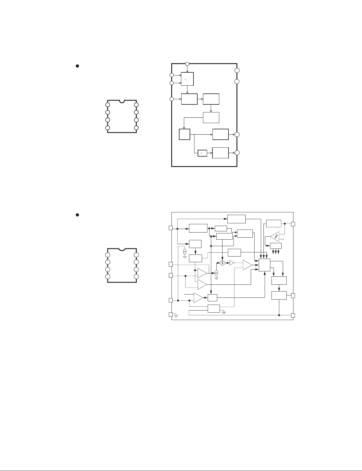
CY2302SXC-1T (XW492A0R)
ES: IC003
PLL (Clock Generator)
FS0
FS1
SB168-ES
FBIN
1
7
4
N
5
VDD
3
GND
FBIN
GND
FS0
1
2
IN
3
4
VDD
8
OUT2
7
6
OUT1
FS1
5
LM3478MM (XZ914A00)
DC: IC90
FET CONTROLLER
ISEN
COMP
AGND
1
2
FB
3
4
8
7
6
5
VIN
FAD/ SD
DR
PGND
IN
FAD/S D
COMP
ISEN
AGND
PHASE
2
DETECTOR
VCO
Ramp
Adjust
FB
Overvoltage
Comparator
350mV
Short-circuit
Comparator
Fixed Frequency
Detect
Soft-start
1.26V
Reference
+
EA
–
–
+
–
+
CHARGE
PUMP
LOOP
FILTER
2
One
Shot
Level
Shifter
OUTPU T
BUFFER
OUTPU T
BUFFER
Oscillator
Slope
Compensation
+
Converter
–
V-l
Shutdown
Detect
Thermal
Shutdown
Converter
6
OUT1
8
OUT2
Set/Blankout
l-V
PWM
Comparator
Undervoltage
Lockout
Bias
Voltages
–
Switch
+
Logic
RS
Switch
Driver
VIN
7.2V
Q
DR
PGND
29
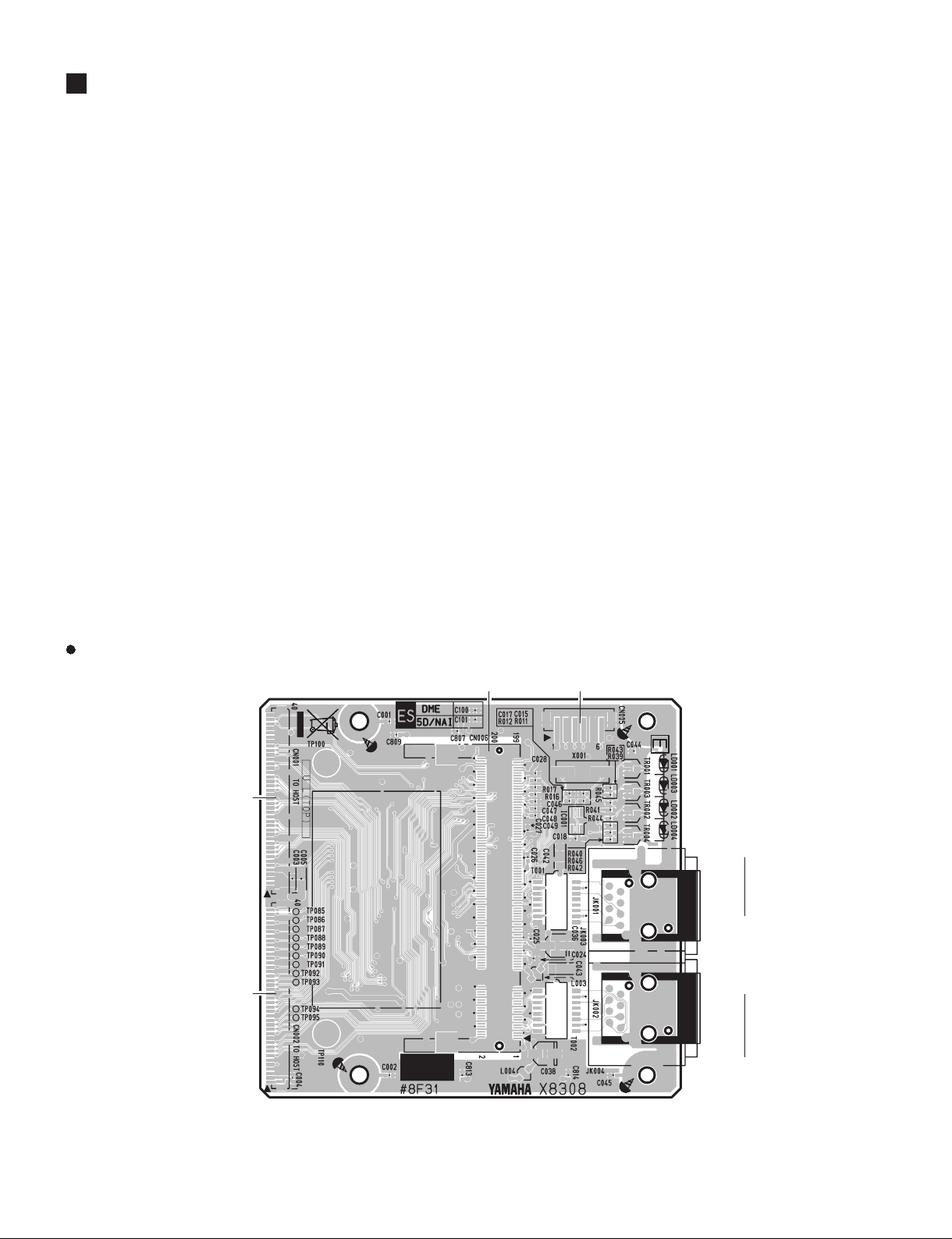
SB168-ES
CIRCUIT BOARDS(シート基板図)
DA Circuit Board (X4169D0) ................................................................................................32/33
DC Circuit Board (YA016C0) ................................................................................................34/35
DM Circuit Board (YA015C0) ......................................................................................36/37/38/39
ES Circuit Board (X8308E0) .................................................................................................30/31
HAAD2 Circuit Board (X6023C0) .........................................................................................40/42
LD1 Circuit Board (YA016C0) ....................................................................................................44
LD2 Circuit Board (YA016C0) ....................................................................................................45
PS Circuit Board (YA016C0) ......................................................................................................31
SW Circuit Board (YA016C0) .....................................................................................................31
Note: See parts list for details of circuit board component parts.
注 : シートの部品詳細はパーツリストをご参照ください。
ES Circuit Board
to DM-CN602
to DM-CN603
N.C.to AVDM-ES Circuit board
IN
EtherSound
OUT
30
Component side
2NA-WJ37400
(部品側)
 Loading...