Yamaha RC-SREV1, DB-SREV1 Service Manual
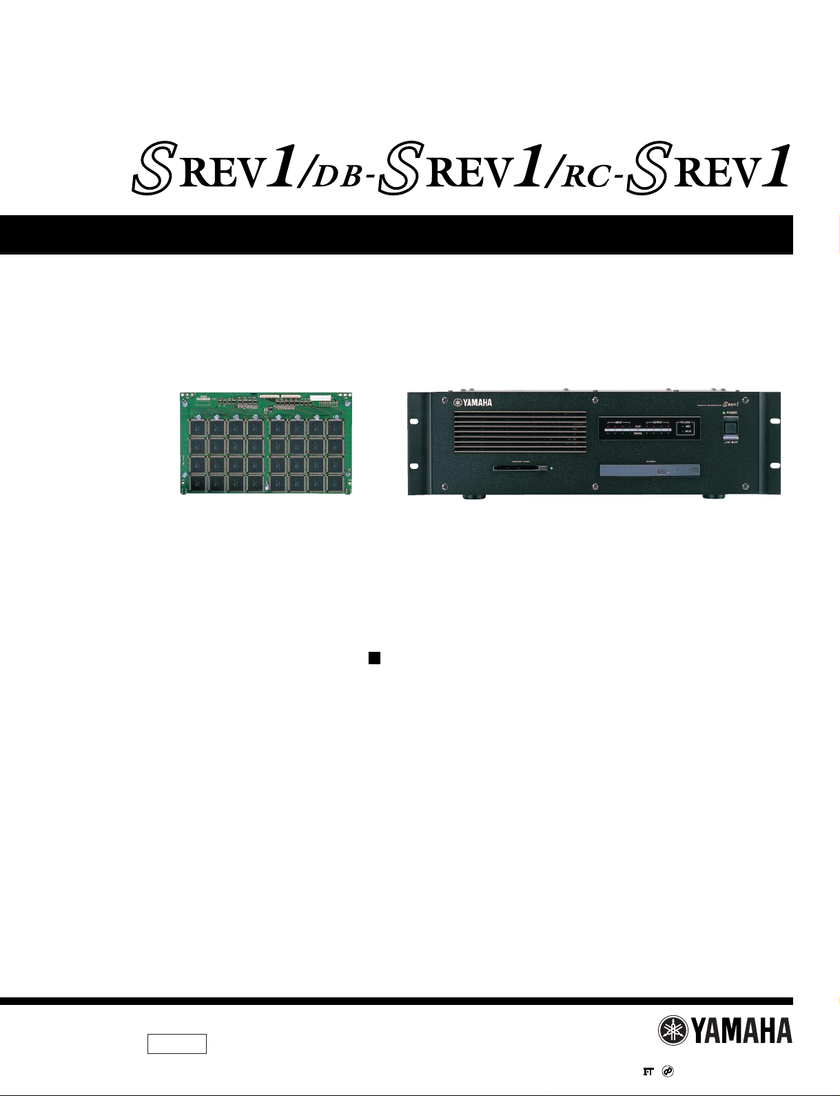
SERVICE MANUAL
PA 1/2
011555
HAMAMATSU, JAPAN
1.415K-0671 Printed in Japan '01.02
CONTENTS
SPECIFICATIONS············································································ 3
PANEL LAYOUT··············································································· 4
CIRCUIT BOARD LAYOUT ······························································ 5
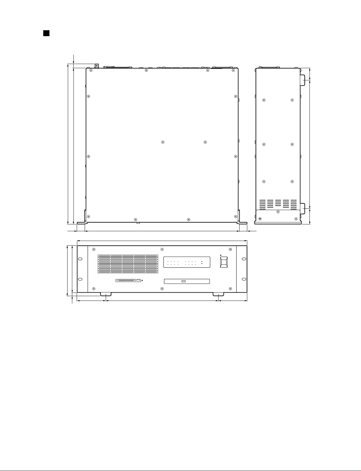
DIMENSIONS ··················································································· 6
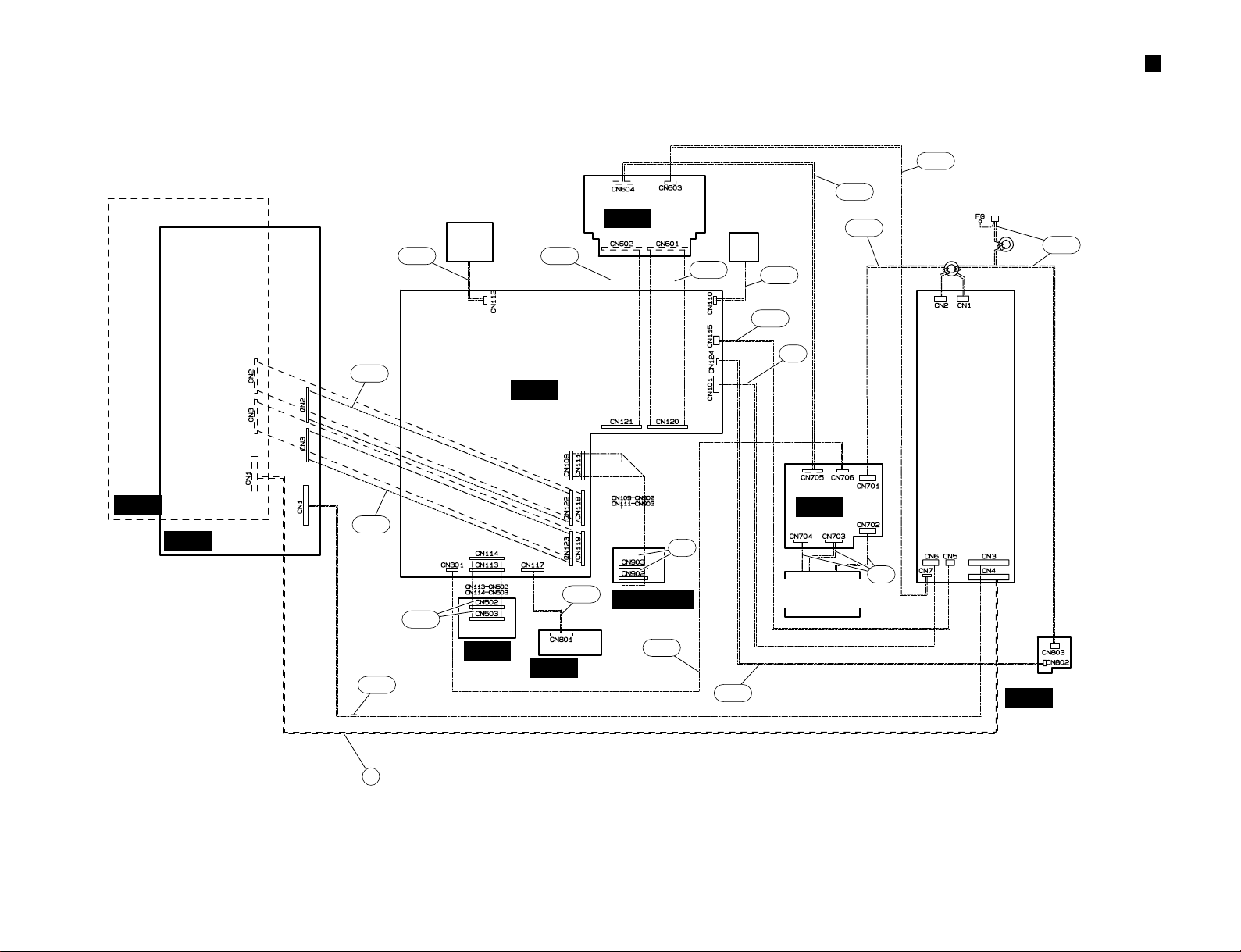
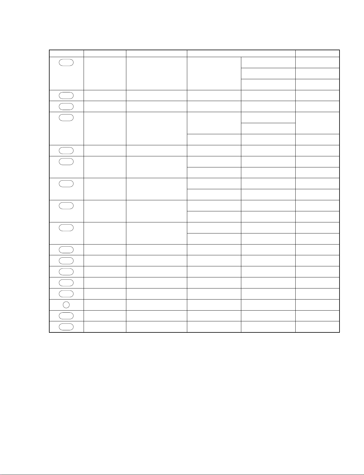
WIRING····························································································· 7
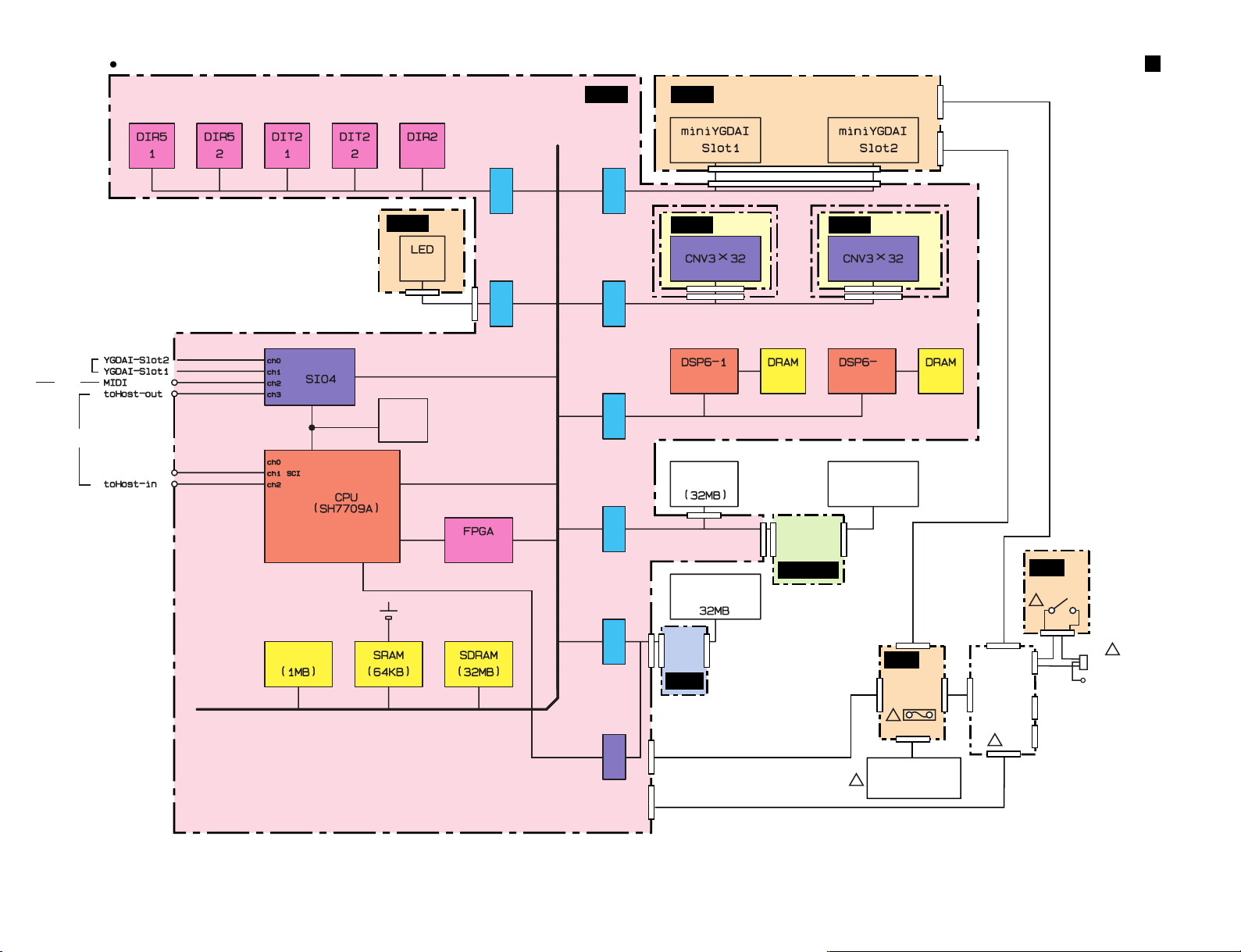
BLOCK DIAGRAM············································································ 9
DISASSEMBLY PROCEDURE······················································· 11
I/O CARD INSTALLATION······························································ 16
DB-SREV1 INSTALLATION···························································· 17
LSI PIN DESCRIPTION·································································· 19
IC BLOCK DIAGRAM······································································ 24
CIRCUIT BOARDS ········································································· 29
TEST PROGRAM ··········································································· 41
ERROR MESSAGES······································································ 44
MIDI IMPLEMENTATION CHART·················································· 46
PARTS LIST
RC-SREV1 SERVICE MANUAL
SREV1/RC-SREV1 OVERALL CIRCUIT DIAGRAM
SREV1: 20001225-500000
RC-SREV1: 20001225-150000
DB-SREV1: 20001225-200000
This document is printed on chlorine free (ECF) paper with soy ink.
SAMPLING REVERBERATOR/
DSP EXPANSION BOARD/REMOTE CONTROLLER
•
DB-SREV1
•
SREV1
SREV1
2
WARNING: CHEMICAL CONTENT NOTICE!
The solder used in the production of this product contains LEAD. In addition, other electrical/electronic and/or plastic (where
applicable) components may also contain traces of chemicals found by the California Health and Welfare Agency (and possibly
other entities) to cause cancer and/or birth defects or other reproductive harm.
DO NOT PLACE SOLDER, ELECTRICAL/ELECTRONIC OR PLASTIC COMPONENTS IN YOUR MOUTH FOR ANY REASON
WHAT SO EVER!
Avoid prolonged, unprotected contact between solder and your skin! When soldering, do not inhale solder fumes or expose eyes
to solder/flux vapor!
If you come in contact with solder or components located inside the enclosure of this product, wash your hands before handling
food.
IMPORTANT NOTICE
This manual has been provided for the use of authorized Yamaha Retailers and their service personnel. It has been assumed that
basic service procedures inherent to the industry, and more specifically Yamaha Products, are already known and understood by
the users, and have therefore not been restated.
WARNING: Failure to follow appropriate service and safety procedures when servicing this product may result in personal
injury, destruction of expensive components and failure of the product to perform as specified. For these
reasons, we advise all Yamaha product owners that all service required should be performed by an authorized
Yamaha Retailer or the appointed service representative.
IMPORTANT: This presentation or sale of this manual to any individual or firm does not constitute authorization, certification,
recognition of any applicable technical capabilities, or establish a principal-agent relationship of any form.
The data provided is belived to be accurate and applicable to the unit(s) indicated on the cover. The research engineering, and
service departments of Yamaha are continually striving to improve Yamaha products. Modifications are, therefore, inevitable and
changes in specification are subject to change without notice or obligation to retrofit. Should any discrepancy appear to exist,
please contact the distributor's Service Division.
WARNING: Static discharges can destroy expensive components. Discharge any static electricity your body may have
accumulated by grounding yourself to the ground bus in the unit (heavy gauge black wires connect to this bus).
IMPORTANT: Turn the unit OFF during disassembly and parts replacement. Recheck all work before you apply power to the
unit.
WARNING
Components having special characteristics are marked and must be replaced with parts having specification equal to those
originally installed.
LITHIUM BATTERY HANDLING
This product uses a lithium battery for memory back-up.
WARNING: Lithium batteries are dangerous because they can be exploded by improper handling. Observe the following
precautions when handling or replacing lithium batteries.
Leave lithium battery replacement to qualified service personnel.
Always replace with batteries of the same type.
When installing on the PC board by soldering, solder using the connection terminals provided on the battery cells.
Never solder directly to the cells. Perform the soldering as quickly as possible.
Never reverse the battery polarities when installing.
Do not short the batteries.
Do not attempt to recharge these batteries.
Do not disassemble the batteries.
Never heat batteries or throw them into fire.
ADVARSEL!
Lithiumbatteri-Eksplosionsfare ved fejlagtig håndtering. Udskiftning må kun ske med batteri af samme fabrikat og type. Levér det
brugte batteri tilbage til leverandøren.
VARNING
Explosionsfara vid felaktigt batteribyte.
Använd samma batterityp eller en ekvivalent typ som rekommenderas av apparattillverkaren.
Kassera använt batteri enligt fabrikantens instruktion.
VAROITUS
Paristo voi räjähtää, jos se on virheellisesti asennettu.
Vaihda paristo ainoastaan laitevalmistajan suosittelemaan tyyppiin.
Hävitä käytetty paristo valmistajan ohjeiden mukaisesti.
The following information complies with Dutch Official Gazette 1995. 45; ESSENTIALS OF ORDER ON THE COLLECTION OF
BATTERIES.
• Please refer to the diassembly procedure for the removal of Back-up Battery.
• Leest u voor het verwijderen van de backup batterij deze beschrijving.
SPECIFICATIONS
SREV1
3
IMPORTANT NOTICE FOR THE UNITED KINGDOM
Connecting the Plug and Cord
IMPORTANT. The wires in this main lead are coloured in
accordance with the following code:
BLUE: NEUTRAL
BROWN: LIVE
As the colours of the wires in the main lead of this apparatus may not
correspond with the coloured markings identifying the terminals in
your plug, proceed as follows:
The BLUE wire must be connected to the terminal that is marked with
the letter N (or coloured BLACK).
The BROWN wire must be connected to the terminal that is marked
with the letter L (or coloured RED).
Be certain that neither core is connected to the earth terminal of the
three pin plug.
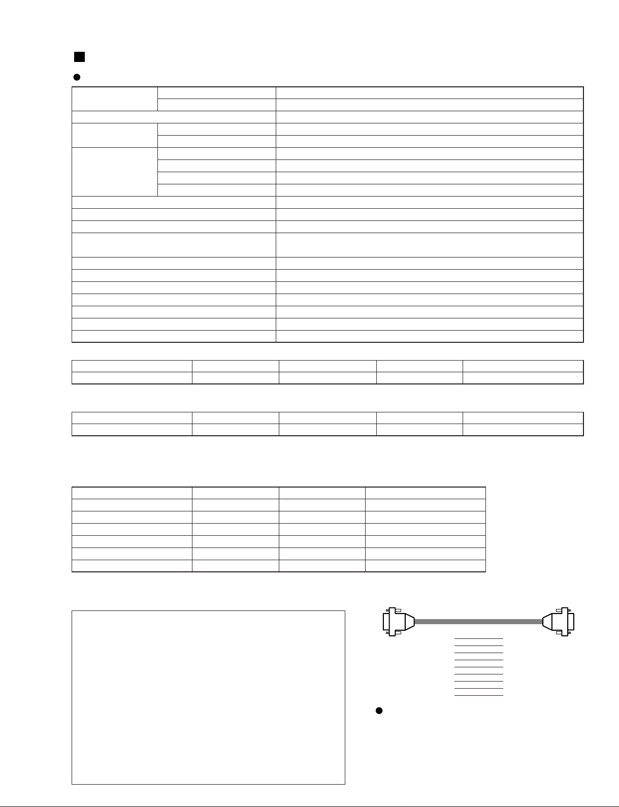
Sampling rate
Internal
External
Internal processing
Program Memories
2-channel, 4-channel mode
2-channel x2 mode
Indicators
INPUT
OUTPUT
FS LOCK
Others
PC Card slot
CD-ROM drive
Cooling fan
Power requirements
Power consumption
Dimensions (W x H x D)
Weight
Free-air operating temperature
Power cord length
Supplied accessories
Options
48 kHz
44.1 kHz or 48 kHz
32 bit
6 (P01–P06)
12 (P01–P12)
SIGNAL x4 (–34 dB), CLIP x4
SIGNAL x4 (–34 dB), CLIP x4
48K, 44.1K
POWER, PC Card, CD-ROM
PCMCIA (Type II), PC Card ATA spec, FAT16
ISO9660 Level 2 format
x2
U.S.A. & Canada 120 V AC, 60 Hz
Europe 230 V AC, 50 Hz
120 W
480 x 141.7 x 451.8 mm (18.9 x 5.6 x 17.8 inches)
11.5 kg (25.3 lbs)
5˚ C to 40˚ C (41˚ F to 104˚ F)
2.5 m
Power cord, CD-ROM (Reverb programs, data), Owner’s Manual
RC-SREV1, DB-SREV1, MY8-AD, MY4-AD, MY4-DA, MY8-AT, MY8-AE, MY8-TD
Connection
DIGITAL IN 1, 2
Format
AES/EBU
Data Length
24 bit
Level
RS-422
Connector
XLR-3-31 type *
1
Digital Input Specifications
*1. XLR-3-31 type connectors are balanced (pin 1–ground, pin 2–hot (+), and pin 3–cold (–).
Connection
DIGITAL OUT 1, 2
Format
AES/EBU *
1
Data Length
24 bit
Level
RS-422
Connector
XLR-3-32 type *
2
Digital Output Specifications
Connection
SERIAL 1, 2
MIDI IN
MIDI OUT
WORD CLOCK IN
REMOTE
SLOT (x2)
Format
—
MIDI
MIDI
—
—
mini YGDAI
Level
RS-422
—
—
TTL 75 Ω
RS-422
—
Connector
8-pin mini DIN
5-pin DIN
5-pin DIN
BNC
9-pin D-sub (female)
—
Control I/O Specifications
*1. Channel status: Type: 2 audio channels.
Sampling rate: depends on internal configuration.
*2. XLR-3-32 type connectors are balanced (pin 1–ground, pin 2–hot (+), and pin 3–cold (–).
SREV1
Remote Cable Wiring Diagram
SREV1
9-pin D-sub
(male)
NC 1
RX– 2
TX+ 3
NC 4
+12V 5
NC 6
RX+ 7
TX– 8
GND 9
1 NC
2 TX–
3 RX+
4 NC
5 +12V
6 NC
7 TX+
8 RX–
9 GND
RC-SREV1
9-pin D-sub
(female)
DB-SREV1
Dimensions (W x H x D): 195 x 15 x 330 mm
Weight: 0.5 kg
Supplied accessories: FPC (Flat Cable) x2
Screw
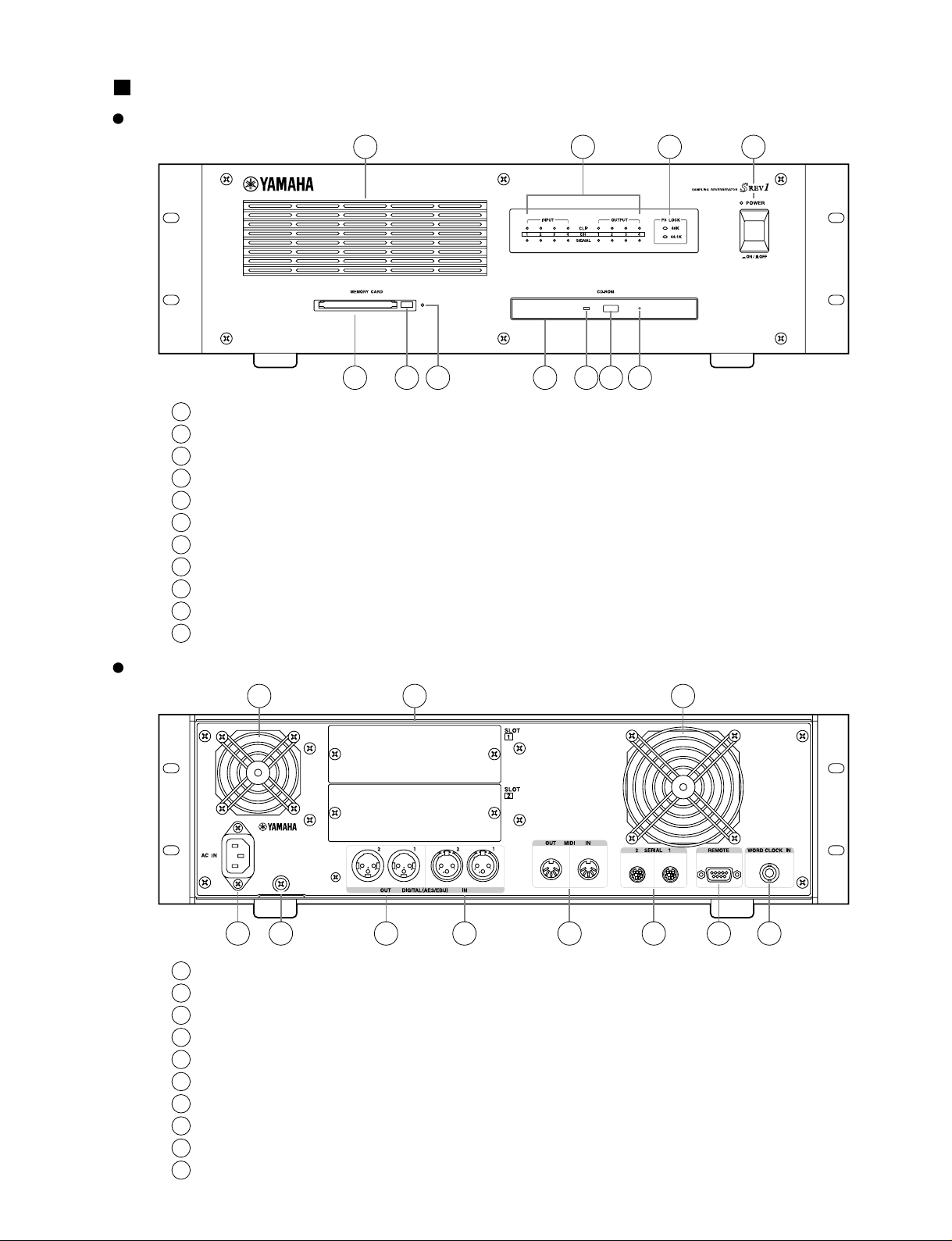
1
5 6 7 8 9 10 11
12 13 12
14 15 16 17 18 19 20 21
2 3 4
1
Air Inlet
2
INPUT and OUTPUT signal indicators
3
FS LOCK indicators
4
POWER switch & indicator
5
MEMORY CARD slot
6
Memory card eject button
7
Memory card activity indicator
8
CD-ROM drive
9
Disc activity indicator
10
CD-ROM eject button
11
Emergency disc eject hole
12
Cooling fan outlets
13
SLOTs 1 & 2
14
AC IN connector
15
Grounding screw
16
DIGITAL OUT (AES/EBU) connectors
17
DIGITAL IN (AES/EBU) connectors
18
MIDI IN & OUT ports
19
SERIAL 1 & 2 ports
20
REMOTE port
21
WORD CLOCK IN connector
PANEL LAYOUT
SREV1
4
Rear Panel
Front Panel

SUB 4/4
SUB 4/4
SUB 3/4PCM
SUB 1/4
SUB 2/4
CNV
CNV
CPU
CN117
CN101
CN124
CN115
CN110
CN301
CN801
CN803
CN704 CN703
CN702
CN701
CN706CN705
CN604 CN603
CN802
CN1
CN1
CN7
CN3
CN4
Power Supply Unit
(DB-SREV1)
AC Inlet
Power
transformer
Power Supply Unit
CN5
CN803
CN802
CN6
3NA-V651940-3,4
DC Fan Motor
Fan
Fan
CD-ROM Drive
DC Fan Motor
SUB 2/4
CD-ROM
PCM
CNV
CNV
(DB-SREV1)
SREV1
5
CIRCUIT BOARD LAYOUT
Top View
Bottom View
SREV1
6
DIMENSIONS
480
132
141.7
9.7
31881 81
437
21.5 21.5
43.5 34362.5
440 11.8
451.8
Unit: mm
CNV
CNV
(DB-SREV1)
PCM
SUB 3/4
CD-ROM
CPU
FAN
(V5789100)
SUB 2/4
FAN
(V3125300)
SUB 1/4
Power Transformer
Power Supply Unit
SUB 4/4
AC Inlet
3NA-V651940-2
200 680
680
160
710
240
CN705
720
140
730
240
750
CN706
670
440
660
740
650
650
A
SREV1
7
WIRNIG
440
650
660
670
680
710
720
730
740
750
CN705
CN706
Power Transformer SUB 1/4-CN702
SUB 1/4-CN703
SUB 1/4-CN704
4P
6P
5P
Power Transformer
Connector Assembly & Unit
Part No.
XY916A00(J)
XY917A00(U, V)
XY918A00(H,B,W)
Location Destination Remarks
CPU-CN117
CPU-CN122
CPU-CN123
CPU-CN113
CPU-CN114
CPU-CN109
CPU-CN111
CPU-CN120
CPU-CN121
SUB 3/4-CN801 9P
CNV-CN2 30P
CNV-CN3 30P
PCM-CN502 30P
PCM-CN503 30P
CDROM-CN902 25P
CDROM-CN903 25P
SUB 2/4-CN601 36P
SUB 2/4-CN602 36P
KR(VR79270)
MFA30100
MFA30100
MFA25300
MFA36080
CPU-CN115
Power Supply Unit-CN5
2PREM-PS(V651290)
CPU-CN101
Power Supply Unit-CN6
4PCPU-PS(V651300)
SUB 2/4-CN603
Power Supply Unit-CN7
4PYGDA-PS(V651310)
CNV-CN1
Power Supply Unit-CN3
10PCNV1-PS(V651320)
CPU-CN124 SUB 4/4-CN802
SUB 2/4-CN604
2PKR(VR78120)
A
CNV(DB-SREV1)-CN1
Power Supply Unit-CN4
10PCNV(Option)-PS(V651320)
SUB 1/4-CN705
CPU-CN301
7PB&CVY914700
SUB 1/4-CN706 4PB&CVQ613000
140
Fan CPU-CN110 3PFanV3125300
160
DC Fan Motor CPU-CN112 3PDC Fan MotorV5789100
200
AC Inlet
SUB 1/4-CN701
SUB 4/4-CN803
Power Supply Unit-CN1
Power Supply Unit-CN2
3P
4P/3P
ACINV6512600
240
SREV1
8
CNV
CPU SUB 2/4
SUB 3/4
SUB 1/4
SUB 4/4
CNV
(
DB-SREV1
)
CN2,3
CN117
CN301
CN113,
114
CN101,115
IC123,137,138
CA [4,14-25]
CD [0-7], CA [1-6]
CD [0-31], CA [0-21]
CD [0-15]
CA [1-3]
CD [0-15]
CA [1-7]
CD [0-31]
CA [2-9]
YD [1-15] YA [0-10]
IC150
(28P)
IC151
(28P)
IC148
(16P)
IC149
(16P)
IC165
(44P)
CN801
SLOT 1,2
MIDI
SERIAL
REMOTE
IC161,162
(20P)
IC155,156,167
(20P)
IC163,164
(16P)
IC132
(16P)
IC113
(44P)
IC114
(48P)
IC105
(28P)
IC107
(48P)
IC108,
109
IC111,112
CN2,3
CN122,123
CN606
CN602
CN121
CN605
CN603
CN604
CN118,119
D-FF
BUFFER
IC127-131
BUFFER
IC177-179
BUFFER
IC180-184
(20P)
IC159
(176P)
IC153,154
(42P)
IC140,141
(42P)
IC143
(176P)
BUFFER
IC173-177
BUFFER
BUFFER
D-FF
2
14,15
16,17
20,21
23
166
174
1
X102
8MHz
Lithium Battery
BT101
32
156
112,113
FLASH-ROM
CF CARD
MEMORY
4MB 4MB
Data bus
Address bus
PCMCIA POWER
INTERFACE SW
PCM
CN501
CN502,
503
CD-ROM
CN901
CN902,
903
CN109,
111
CN108
CN701
CN7
CN2
CN3
CN4
CN5,6
CN706
CN705
CN702-704
CN1
to CNV-CN1
to CNV(DB-SREV1)-CN1
CN803
FUSE
!
!
!
!
!
Power
Supply
Unit
POWER
Power
Transformer
AC INLET
FG
2
CPU Section
CD-ROM
Drive
MEMORY CARD
(PCMCIA)
SREV1
9
BLOCK DIAGRAM
38CA1-8818094-2
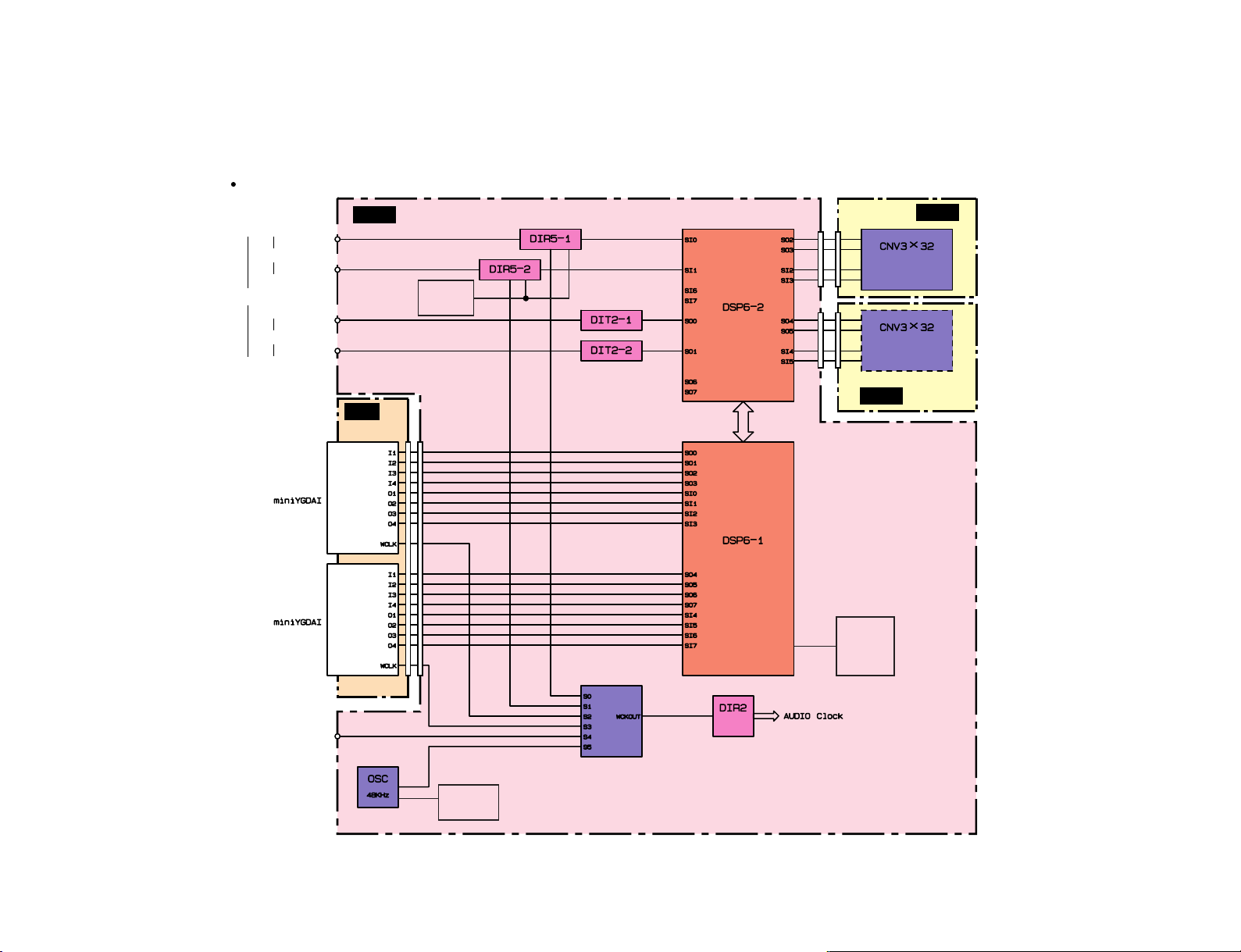
CN2, 3
CN122, 123
CN2, 3
CN118,
119
6755
56
65716
15 10
15 10
716
65
66
67
68
55
56
57
58
69
3
70
71
72
59
60
61
62
365
9
4
3
2
1
15
14
1
66
68
57
58
IC1~16, 35~50
(128P)
69
70
59
60
IC1~16, 35~50
(128P)
IC143
(176P)
IC148 (16P)
135
IC150 (28P)
13
5
IC151 (28P)
IC149 (16P)
IC302
(14P)
IC159
(176P)
IC165
(44P)
IC160
(15P)
CN606
CN601
CN120
CN605
(DB-SREV1)
X104
60MHz
MULTIPLEXER
COUNTER
X301
6.144MHz
X103
25.6MHz
SLOT 1
SLOT 2
JK108
WORD CLOCK IN
1
1
JK104
JK105
JK106
JK107
1
2
IN
1
2
OUT
DIGITAL (AES / EBU)
AUDIO Section
SUB 2/4
CPU
CNV
CNV
SREV1
10
38CA1-8818094-3

SUB 1/4
[125]
Power transformer
[150]
CNV
PCM
[360] [B] [B][360]
(DB-SREV1)
CNV
Fig. 2
(DB-SREV1)
<Top View> <SEC A-A'>
[B]: Bind Head Tapping Screw-B 3.0X8 MFZN2BL (EP600190)
[125]: Bind Head Tapping Screw-B 3.0X8 MFZN2BL (EP600190)
[150]: Bind Head Tapping Screw-B A4.0X8 MFZN2BL (VC688800)
[360]: Bind Head Tapping Screw-B 3.0X8 MFZN2BL (EP600190)
[460]: Bind Head Tapping Screw-B 3.0X8 MFZN2BL (EP600190)
CNV
PCM
[B]
[460] [460]
A
A'
Fig. 1
[850]: Bind Head Tapping Screw-B A4.0X8 MFZN2BL (VC688800)
[850] x14
Top cover
SREV1
11
DISASSEMBLY PROCEDURE
1. Top Cover (Time required: about 5 minutes)
1-1 Remove the fourteen (14) screws marked [850]. The top
cover can then be removed. (Fig. 1)
2. DB-SREV1 (CNV Circuit Board)
(Time required: about 8 minutes)
2-1 Remove the top cover. (See procedure 1.)
2-2 Remove the two (2) screws marked [A] and the two (2)
screws marked [B]. The CNV circuit board (DB-SREV1)
can then be removed. (Fig. 2, 3)
3.
CNV Circuit Board
(Time required: about 10 minutes)
3-1 Remove the top cover. (See procedure 1.)
3-2 Remove the DB-SREV1 CNV circuit board, if it is being
installed. (See procedure 2.)
3-3 Remove the two (2) screws marked [350] and the two (2)
screws marked [360]. The CNV circuit board can then be
removed. (Fig. 2, 3)
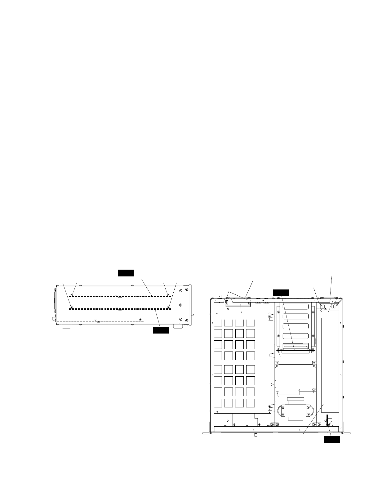
Fig. 4
Power supply unit
Finger guard
Fan support metal
<Top View>
[120]: Bind Head Tapping Screw-B 3.0X8 MFZN2BL (EP600190)
SUB 4/4
[120] x4
SUB 2/4
Fan guide
Fig. 3
[A]: Bind Head Screw A3.0X6 MFZN2BL (VP156600)
[350]: Bind Head Screw A3.0X6 MFZN2BL (VP156600)
<Left Side View>
(DB-SREV1)
CNV
[A] [A][350] [350]
CNV
DC fan motor
Fan
Fan guard
SREV1
12
4. PCM Circuit Board
(Time required: about 15 minutes)
4-1 Remove the top cover. (See procedure 1.)
4-2 Remove the DB-SREV1 CNV circuit board, if it is being
installed. (See procedure 2.)
4-3 Remove the CNV circuit board. (See procedure 3.)
4-4 Remove the two (2) screws marked [460]. The PCM
circuit board can then be removed. (Fig. 2)
5.
Power Transformer, SUB 1/4 Circuit Board
(Time required: about 8 minutes each)
5-1 Remove the top cover. (See procedure 1.)
5-2 Power Transformer
Remove the four (4) screws marked [150]. The power
transformer can then be removed. (Fig. 2)
5-3 SUB 1/4 Circuit Board
Remove the two (2) screws marked [125]. The SUB 1/4
circuit board can then be removed. (Fig. 2)
6. SUB 2/4 Circuit Board
(Time required: about 15 minutes)
6-1 Remove the top cover. (See procedure 1.)
6-2 Remove the power transformer. (See procedure 5-2.)
6-3 Remove the SUB 1/4 circuit board (See procedure 5-3.)
6-4 Remove the four (4) screws marked [120]. The SUB 2/4
circuit board can then be removed. (Fig. 4)
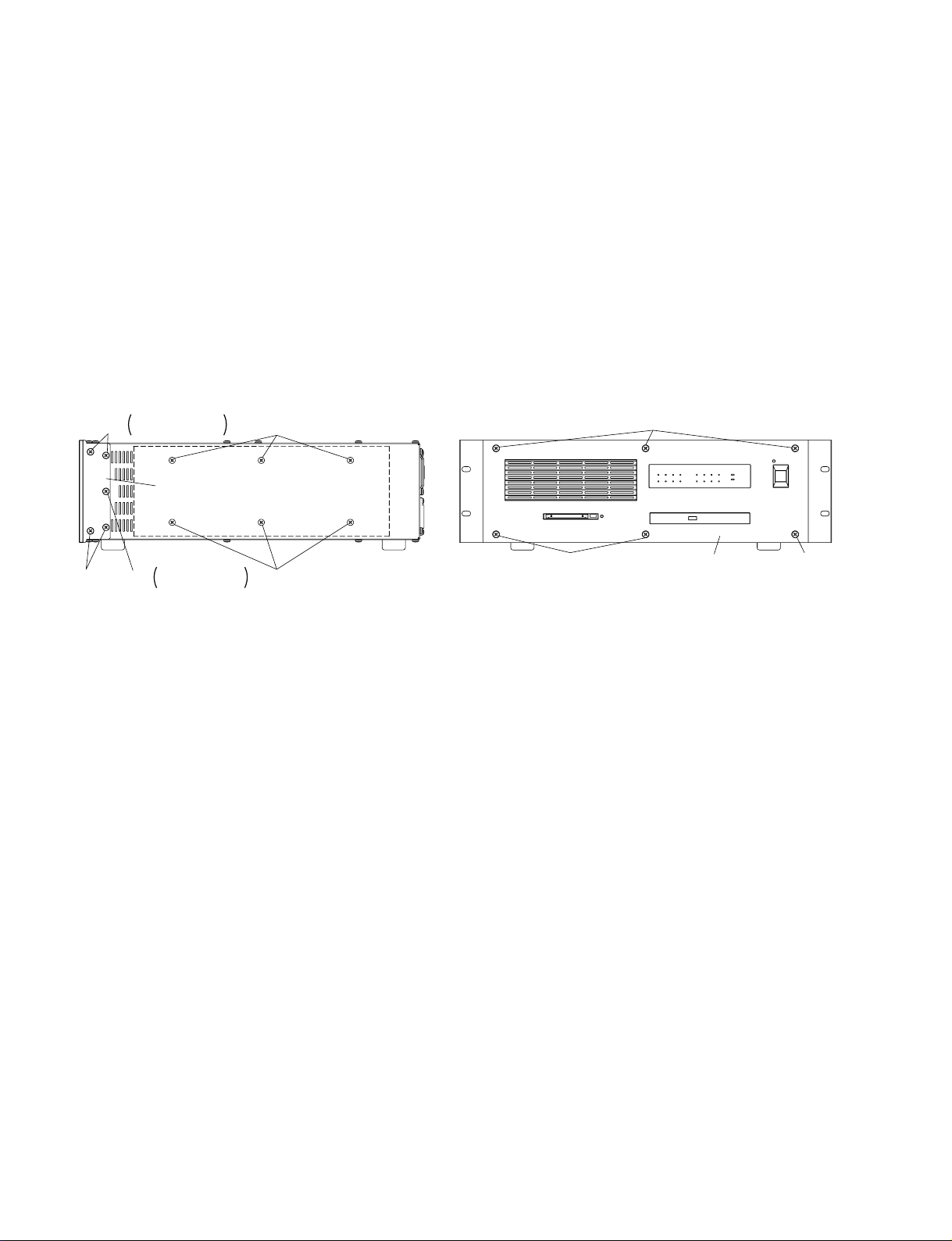
Fig. 6
[570]: Oval Head Screw B4.0X10 MFZN2BL (V6221000)
[570]
<Right Side View> <Front View>
Fig. 5
[60]: Bind Head Screw A4.0X8 MFZN2BL (VP156800)
[600]: Oval Head Screw B4.0X10 MFZN2BL (V6221000)
[610]: Oval Head Screw 4.0X8 MFZN2BL (VS153600)
[60]
[610]
Front panel
[60][610] [600]
Mount bracket
Right side: 4pcs
Left side: 4pcs
Right side: 1pc.
Left side: 1pc.
[570] [570]
SREV1
13
7. Power Supply Unit
(Time required: about 10 minutes)
7-1 Remove the top cover. (See procedure 1.)
7-2 Remove the six (6) screws marked [60]. The power supply
unit can then be removed. (Fig. 4, 5)
8. Front Panel(Time required: about 10 minutes)
8-1 Remove the top cover. (See procedure 1.)
8-2 Remove the two (2) screws marked [600] and the eight (8)
screws marked [610]. The left and rihgt mount brackets
can then be removed. (Fig. 5)
8-3 Remove the six (6) screws marked [570] The front panel
can then be removed. (Fig. 6)
9.
SUB 3/4 Circuit Board, SUB 4/4 Cir cuit Board
(Time required: about 15 minutes each)
9-1 Remove the top cover. (See procedure 1.)
9-2 Remove the front panel (See procedure 8.)
9-3 SUB 3/4 Circuit Board
Remove the two (2) screws for [410] and pull out the SUB
3/4 circuit board from the two of the sub-chassis. (Fig. 7)
9-4 SUB 4/4 Circuit Board
Pull out the power switch knob. (Fig. 7)
Remove the two (2) screws marked [430]. The SUB 4/4
circuit board can then be removed. (Fig. 4, 7)
10. DC Fan Motor (Time required: about 10 minutes)
10-1 Remove the top cover. (See procedure 1.)
10-2 Remove the four (4) screws marked [230]. The DC fan
motor can then be removed with both the fan guard and the
fan guide. (Fig. 4, 8)
11. Fan(Time required: about 10 minutes)
11-1 Remove the top cover. (See procedure 1.)
11-2 Remove the four (4) screws marked [190]. The Fan can
then be removed with both the finger guard and the fan
support metal. (Fig. 4, 8)
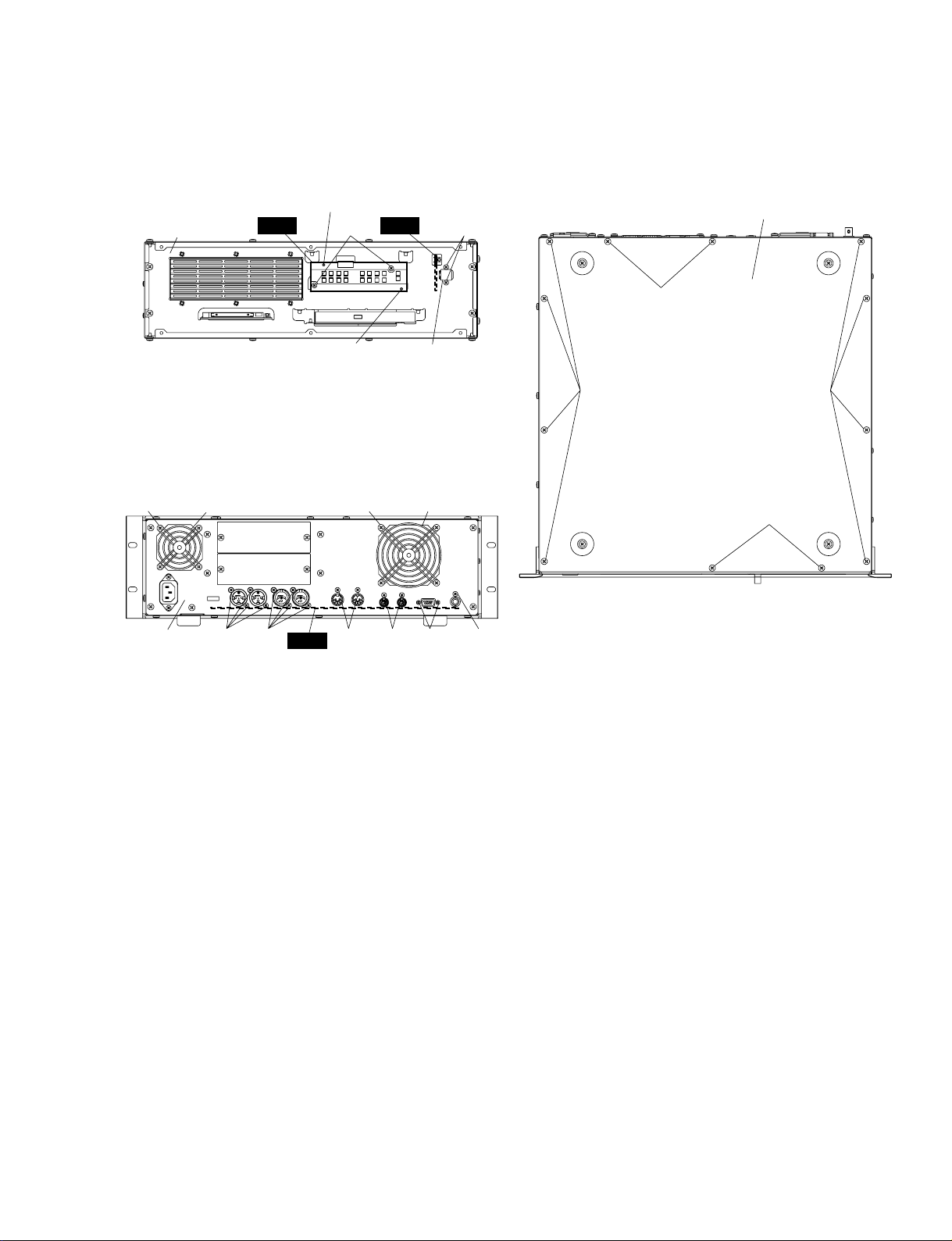
SREV1
14
13 CPU Circuit Board
(Time required: about 10 minutes)
13-1 Remove the bottom cover. (See procedure 12.)
13-2 Remove the two (2) jack sockets marked [290], the three
(3) screws marked [300], the ten (10) screws marked [310],
the screw marked [320] and the two (2) screws marked
[330]. The CPU circuit board can then be removed. (Fig.
8, 10, 11)
14 CD-ROM Circuit Board
(Time required: about 5 minutes)
14-1 Remove the bottom cover. (See procedure 12.)
14-2 Remove the CN angle bracket by removing the two (2)
screws marked [520]. The CD-ROM circuit board can then
be removed with pulling out the connector of the CD-ROM
circuit board from the CD-ROM drive. (Fig. 10)
Fig. 9
[830]: Bind Head Tapping Screw-B A4.0X8 MFZN2BL (VC688800)
<Bottom View>
Bottom cover
[830]
[830]
[830]
Fig. 8
[190]: Bind Head Screw SP 4.0X25 MFZN2BL (VR116500)
[230]: Pan Head Screw SP 4.0X20 MFZN2BL (VR116500)
[300]: Bind Head Screw A3.0X6 MFZN2BL (VP156600)
[310]: Bind Head Tapping Screw-B A3.0X8 MFZN2BL (VP157000)
[410]: Bind Head Tapping Screw-B 3.0X8 MFZN2BL (EP600190)
[430]: Bind Head Screw A3.0X6 MFZN2BL (VP156600)
Fig. 7
<Front View>
<Rear View>
[410] [430]
[230] x4
[300][300][310][310][310] [290]
[190] x4
SUB 3/4 SUB 4/4
Sub chassis
Fan guardFinger guard
Rear panel
[830]
Hook
Hook Power switch knob
CPU
12 Bottom Cover(Time required: about 5 minutes)
12-1 Remove the twelve (12) screws marked [830]. The bottom
cover can then be removed. (Fig. 9)
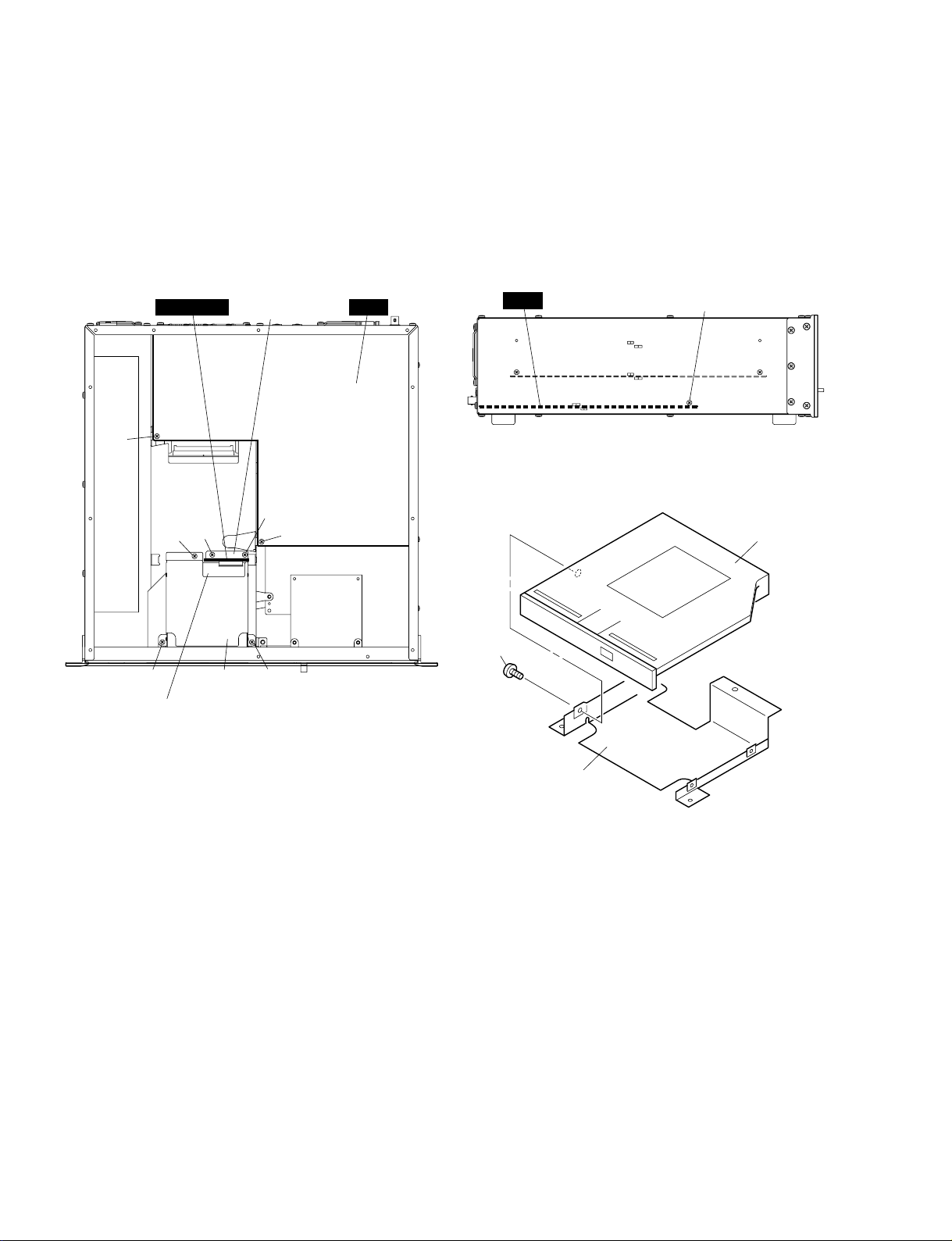
SREV1
15
Fig. 11
[320]: Bind Head Screw A3.0X6 MFZN2BL (VP156600)
Fig. 10
[330]: Bind Head Tapping Screw-B 3.0X8 MFZN2BL (EP600190)
[520]: Bind Head Tapping Screw-B A3.0X8 MFZN2BL (VP157000)
[530]: Bind Head Tapping Screw-B A3.0X8 MFZN2BL (VP157000)
Fig. 12
[500]: Pan Head Screw 2.0X2 MFZN2Y (V6881500)
<Bottom View> <Left Side View>
CD-ROM
[320]
CD-ROM drive
CD-ROM drive
CD angle
CD angle
[330]
[330]
[520]
[520]
[530]
[530]
[500] x4
[530]
CPU
CPU
CN angle bracket
15
CD-ROM Drive(Time required: about 10 minutes)
15-1 Remove the bottom cover. (See procedure 12.)
15-2 Remove the CD-ROM circuit board. (See procedure 14.)
15-3 Remove the three (3) screws marked [530]. The CD-ROM
drive can then be removed with the CD angle. (Fig. 10)
15-4 Remove the CD angle from the CD-ROM drive by
removing the four (4) screws marked [500]. (Fig. 12)
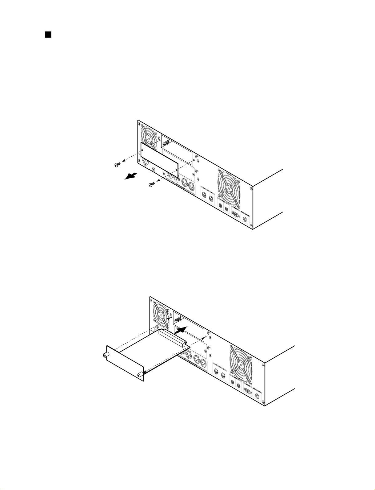
INSTALLING I/O CARDS
SREV1
16
This section explains how to install mini YGDAI cards in the SREV1.
1. Turn off the SREV1.
2. Undo the two fixing screws and remove the slot cover, as shown below.
Keep the cover and fixing screws in a safe place for future use.
3. Insert the card between the guide rails and slide it all the way into the slot, as shown below. You may have to
push firmly to plug the card into the SREV1 connector.
4. Secure the card using the attached thumbscrews. Do not leave the thumb-screws loose, as the card will not be
grounded correctly.
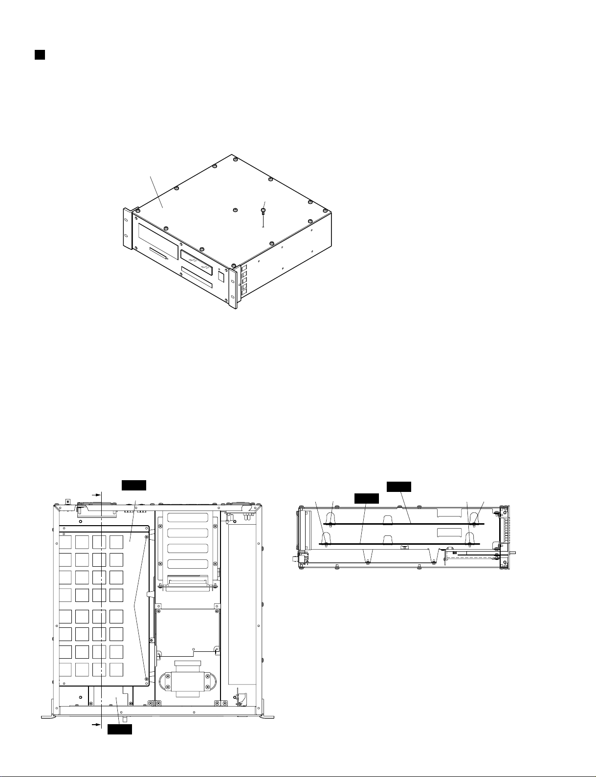
CNV
[360] [B] [B][360]
(DB-SREV1)
CNV
Fig. 2
(DB-SREV1)
<Top View> <SEC A-A'>
[B]: Bind Head Tapping Screw-B 3.0X8 MFZN2BL (EP600190)
[360]: Bind Head Tapping Screw-B 3.0X8 MFZN2BL (EP600190)
CNV
PCM
[B]
A
A'
Fig. 1
[850]: Bind Head Tapping Screw-B A4.0X8 MFZN2BL (VC688800)
[850] x14
Top cover
SREV1
17
DB-SREV1 INSTALLATION
* Before installing the DB-SREV1 (CNV) circuit board,
turn off the SREV1 and disconnect the power cord.
1. Top Cover Removal
Remove the fourteen (14) screws marked [850]. The top
cover can then removed. (Fig. 1)
2. CNV Circuit Board Removal
Remove the two (2) screws marked [350] and the two (2)
screws marked [360]. The CNV circuit board can then be
removed. (Fig. 2, 3)
3. Cables Connection
Connect the two supplied cables to the CPU circuit board
(CN118, CN119) so that the printed side appears as shown
as in Figure 4, and then close the securing clips on each
side of the connectors.
* The two supplied cables are identical.
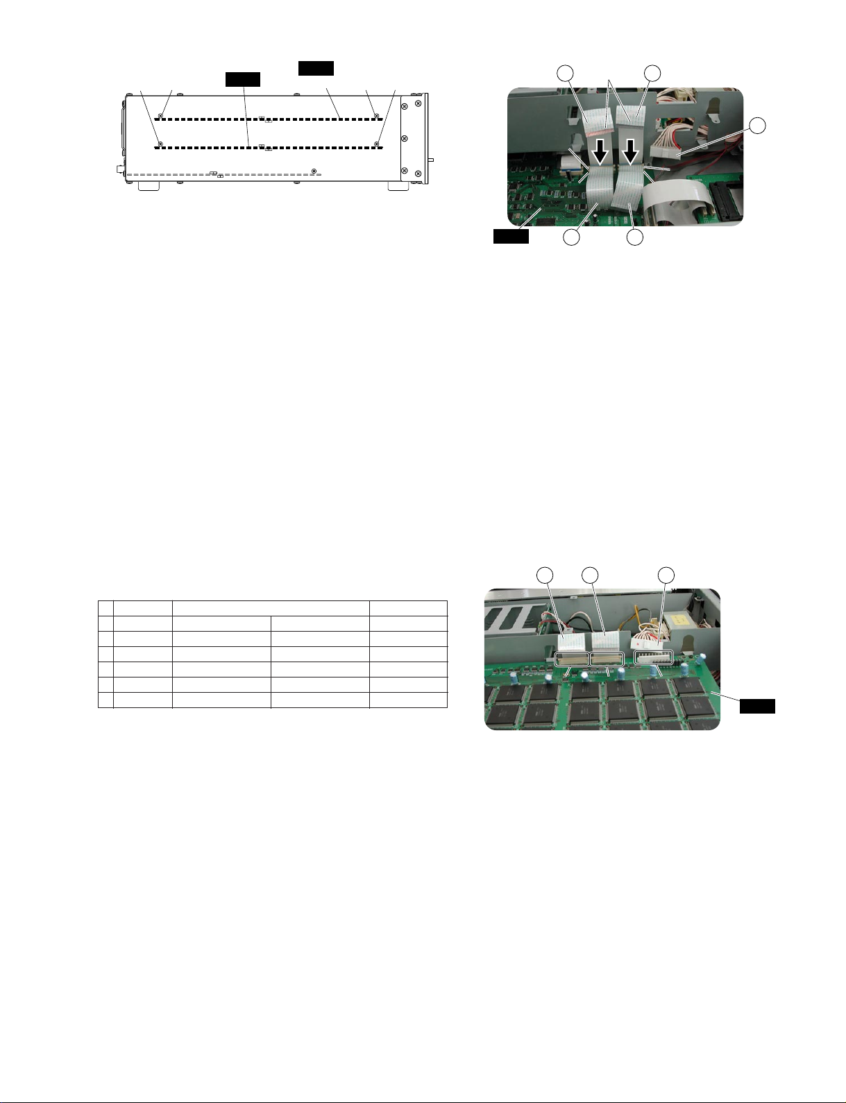
Fig. 3 Fig. 4
[A]: Bind Head Screw A3.0X6 MFZN2BL (VP156600)
[350]: Bind Head Screw A3.0X6 MFZN2BL (VP156600)
<Left Side View>
(DB-SREV1)
CNV
[A] [A][350] [350]
Printed side
CNV
CPU
1 2
3 4
5
CN123CN123
CN119CN119
CN122CN122
CN118CN118
6. Re-attach the SREV1 Top Cover
Replace the fourteen (14) fixing screws marked [850].
The top cover can then be Replaced. (Fig. 1)
7. Checking that the DB-SREV1 (CNV) Circuit
Board is Working Correctly
If the DB-SREV1 (CNV) circuit board is working correctly,
when the SREV1 is turned on the two rows of INPUT and
OUTPUT front panel indicators light up alternately in a
streaming pattern from left to right. If the indicators do not
light up like this, the DB-SREV1 (CNV) circuit board is not
working correctly, in which case you should check that it's
installed in accordance with these instructions.
8. Execute Test Program
Execute test program No. 5 in Section 5-2 and check if
operation is normal. (Refer to page 42.)
Fig. 5
(DB-SREV1)
3 4 6
CN2CN2 CN3CN3 CN1CN1
CNV
SREV1
18
4. CNV Circuit Board Installation
Reinstall the previously removed CNV circuit board,
remembering to replace the two (2) internal fixing screws
marked [360] and two (2) external fixing screws marked
[350]. (Fig. 2, 3)
Reconnect the two cable connectors and the power supply
connector. (Table 1)
5.
DB-SREV1 (CNV) Circuit Board Installation
5-1 Cut and remove the cable fastener holding the power supply
cable intended for the DB-SREV1(CNV) circuit board.
5-2 Install the DB-SREV1 (CNV) circuit board above the
existing CNV circuit board, secure it by using two (2)
internal fixing screws marked [B] and two (2) external
fixing screws marked [A]. (Fig. 2, 3)
5-3 Connect the two cable connectors and the power supply
connector, as shown in Figure 5. (Table 1)
1
2
3
4
5
6
MFA30100
MFA30100
MFA30140
MFA30140
(V6513200)
(V6513200)
CPU-CN122 CNV-CN2
CPU-CN123 CNV-CN3
CPU-CN118
DB-SREV1(CNV)-CN2
CPU-CN119
DB-SREV1(CNV)-CN3
Power Supply Unit-CN3
CNV-CN1
Power Supply Unit-CN4
DB-SREV1(CNV)-CN1
30P/L=100mm
30P/L=100mm
30P/L=140mm
30P/L=140mm
10P
10P
DESTINATION REMERKS
PARTS NO
• Connector Assembly
* Connector assembly listed above are not available as service parts
except MFA30100 and MFA30140.
Table 1
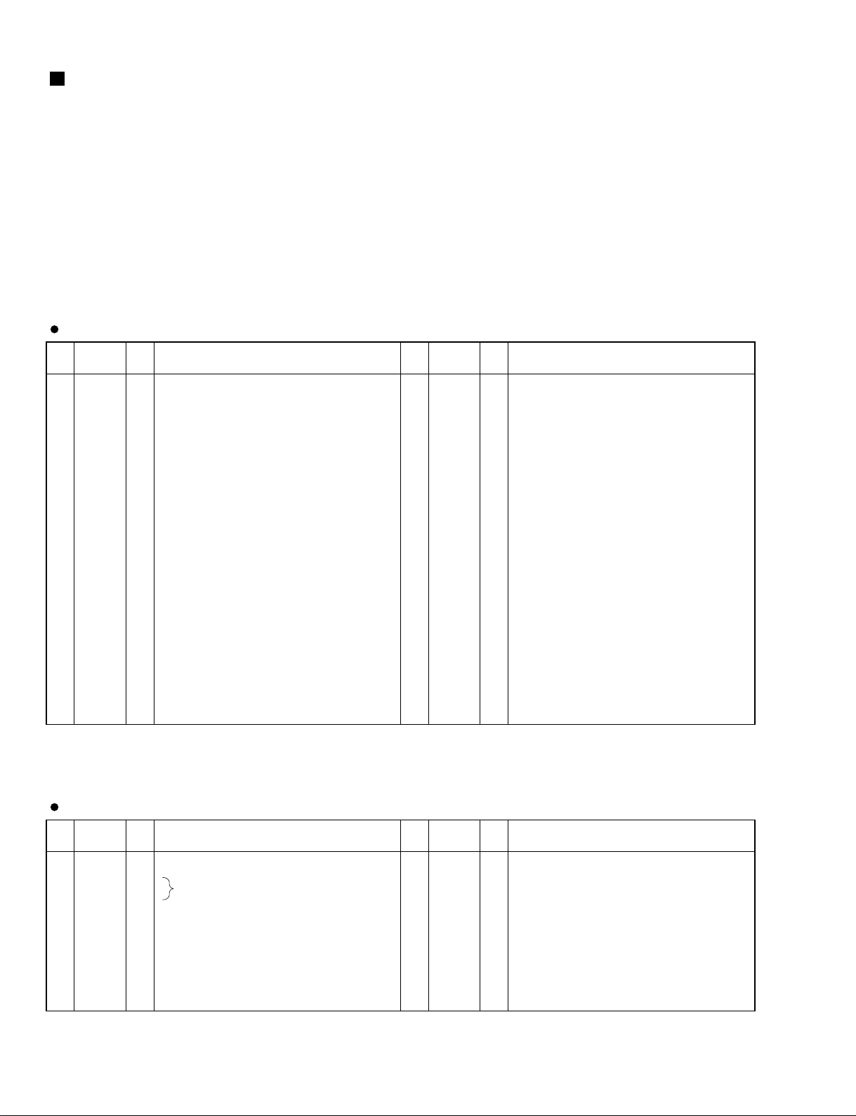
LSI PIN DESCRIPTION
19
PIN
NO.
I/O FUNCTIONNAME
PIN
NO.
I/O FUNCTIONNAME
1
2
3
4
5
6
7
8
9
10
11
12
13
14
15
16
17
18
19
20
21
22
DAUX
HDLT
DOUT
VFL
OPT
SYNC
MCC
WC
MCB
MCA
SKSY
XI
XO
P256
LOCK
Vss
TC
DIM1
DIM0
DOM1
DOM0
KM1
I
O
O
O
O
O
O
O
O
O
I
I
O
O
O
O
I
I
I
I
I
Auxiliary input for audio data
Asynchronous buffer operation flag
Audio data output
Parity flag output
Fs x 1 Synchronous output signal for DAC
Fs x 1 Synchronous output signal for DSP
Fs x 64 Bit clock output
Fs x 1 Word clock output
Fs x 128 Bit clock output
Fs x 256 Bit clock output
Clock synchronization control input
Crystal oscillator connection or external
clock input
Crystal oscillator connection
VCO oscillating clock connection
PLL lock flag
Logic section power (GND)
PLL time constant switching output
Data input mode selection
Data input mode selection
Data output mode selection
Data output mode selection
Clock mode switching input 1
23
24
25
26
27
28
29
30
31
32
33
34
35
36
37
38
39
40
41
42
43
44
RSTN
Vdda
CTLN
PCO
(NC)
CTLP
Vssa
TSTN
KM2
KM0
FS1
FS0
CSM
EXTW
DDIN
LR
Vdd
ERR
EMP
CD0
CCK
CLD
I
I
O
I
I
I
I
O
O
I
I
I
O
O
O
O
I
I
System reset input
VCO section power (+5 V)
VCO control input N
PLL phase comparison output
VCO control input P
VCO section power (GND)
Test terminal. Open for normal use
Clock mode switching input 2
Clock mode switching input 0
Channel status sampling frequency
display output 1
Channel status sampling frequency
display output 0
Channel status output method selection
External synchronous auxiliary input
word clock
EIAJ (AES/EBU) data input
PLL word clock output
Logic section power (+5 V)
Data error flag output
Channel status emphasis control code
output
3-wire type microcomputer interface data
output
3-wire type microcomputer interface clock
input
3-wire type microcomputer interface load
input
YM3436DK (XG948E00) DIR2 (Digital Format Interface Receiver)
CPU: IC165
PIN
NO.
I/O FUNCTIONNAME
PIN
NO.
I/O FUNCTIONNAME
1
2
3
4
5
6
7
8
Vss
MCLK
DM0
DM1
RSTN
WCIN
DIN
V
DD
I
I
I
I
I
I
Ground
Master clock input
DIN/BCLK/WCLK format select
DM1,DM0=0,0 DSP,LDSP (64 bit,LSB first)
DM1,DM0=0,1stereo,DSP (64 bit,MSB first)
DM1,DM0=1,0 DSP2 (128 bit,MSB first)
DM1,DM0=1,1 BB (64 bit,MSB first)
System reset
Word clock input
Digital audio serial data input
Power supply (+5 V)
9
10
11
12
13
14
15
16
MUTE
VFL
CCK/CCB
CIN/UDB
CLD/AUXTN
CNTR/BLKIN
CSM
DOUT
I
I
I
I
I
I
I
O
Mute
Validity flag
C,U bit clock input/C bit data input
C,U bit data input/U bit data input
End of C,U bit input/16,20 bit/24 bit select
32 bit counter reset/Top of block
Channel status input mode select
CSM=0 Asynchronous mode,
CSM=1 Synchronous mode
Digital interface formatted data output
YM3437C-F (XM530A00) DIT2 (Digital Format Interface Transmitter)
CPU: IC148, 149
YM3436DK (XG948E00) DIR2 (Digital Format Interface Receiver)····················································· 19
YM3437C-F (XM530A00) DIT2 (Digital Format Interface Transmitter) ················································ 19
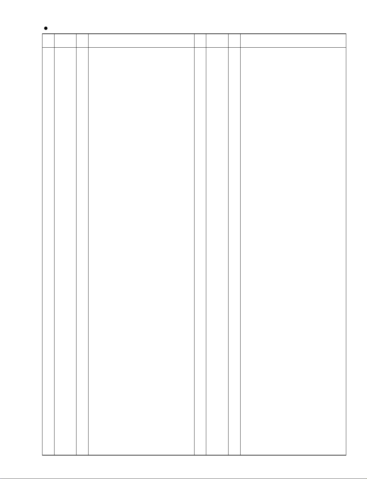
SH7709A (XY065A00) CPU················································································································· 20
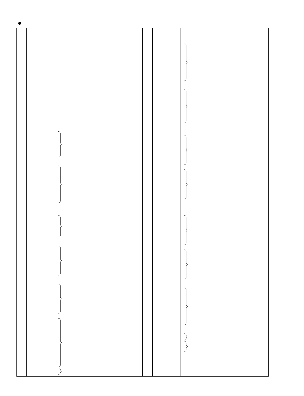
YSS910-S (XV988A00) DSP6 (Digital Signal Processor) ···································································· 21
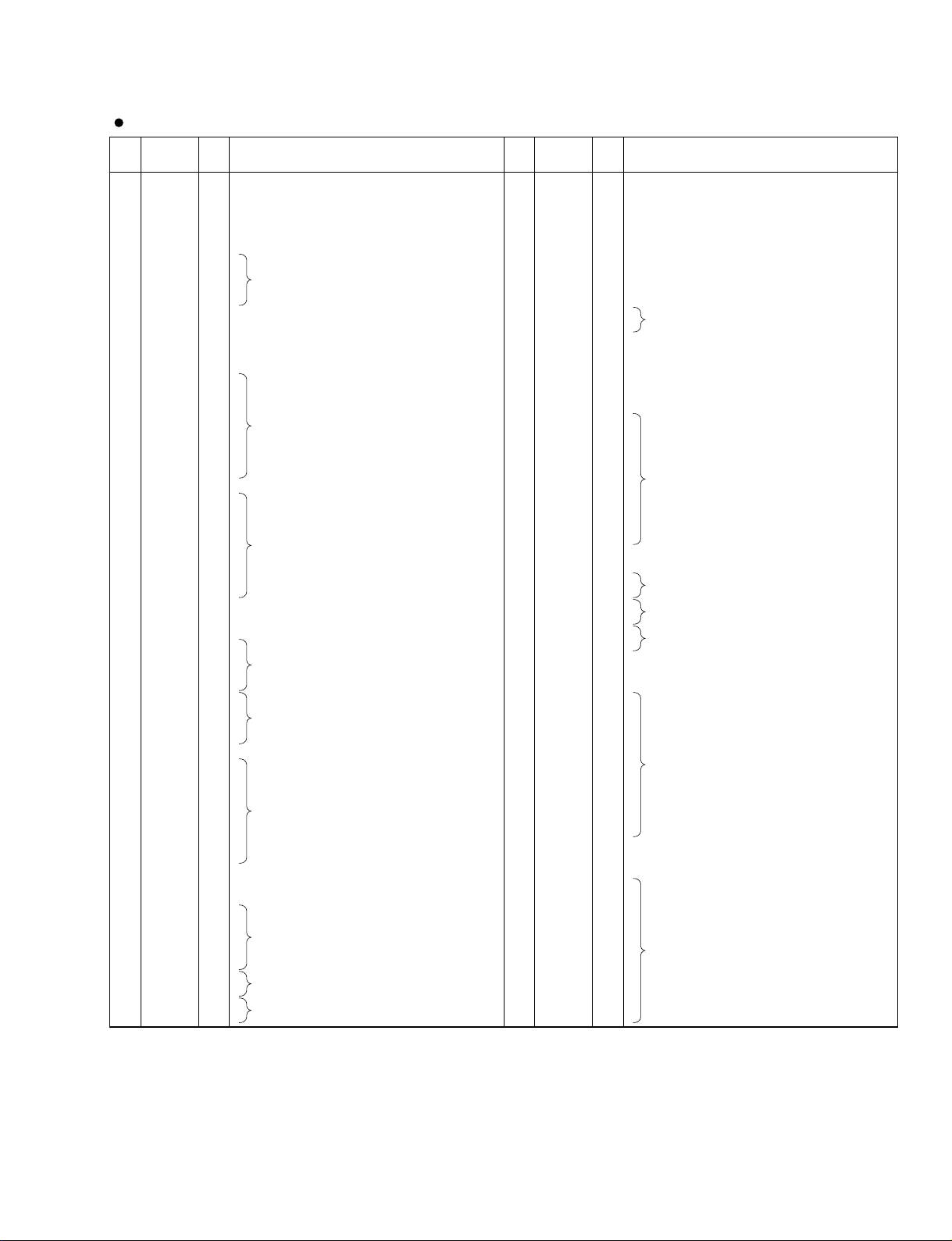
YSS916-H (XW867A00) CNV3 DSP (Convolver)················································································· 22
MBCG46183-129 (XV833A00) Gate Array·························································································· 23
YSD917-ME2 (XW526A00) DIR5 (Digital Format Interface Receiver)················································· 23
1
2
3
4
5
6
7
8
9
10
11
12
13
14
15
16
17
18
19
20
21
22
23
24
25
26
27
28
29
30
31
32
33
34
35
36
37
38
39
40
41
42
43
44
45
46
47
48
49
50
51
52
53
54
55
56
57
58
59
60
61
62
63
64
65
66
67
68
69
70
71
72
73
74
75
76
77
78
79
80
81
82
83
84
85
86
87
88
89
90
91
92
93
94
95
96
97
98
99
100
101
102
103
104
MD1
MD2
Vcc-RTC*1
XTAL2
EXTAL2
Vss-RTC*1
NMI
IRO0/IRL0/PTH[0]
IRO1/IRL1/PTH[1]
IRO2/IRL2/PTH[2]
IRO3/IRL3/PTH[3]
IRO4/PTH[4]
D31/PTB[7]
D30/PTB[6]
D29/PTB[5]
D28/PTB[4]
D27/PYB[3]
D26/PTB[2]
VssO
D25/PTB[1]
VccO
D24/PTB[0]
D23/PTA[7]
D22/PTA[6]
D21/PTA[5]
D20/PTA[4]
Vss
D19/PTA[3]
Vcc
D18/PTA[2]
D17/PTA[1]
D16/PTA[0]
VssO
D15
VccO
D14
D13
D12
D11
D10
D9
D8
D7
D6
VssO
D5
VccO
D4
D3
D2
D1
D0
A0
A1
A2
A3
VssO
A4
VccO
A5
A6
A7
A8
A9
A10
A11
A12
A13
VssO
A14
VccO
A15
A16
A17
A18
A19
A20
A21
Vss
A22
Vcc
A23
VssO
A24
VccO
A25
BS/PTK[4]
RD
WE0/DOMLL
WE1/DOMLU/WE
WE2/DOMUL/ICIORD/PTK[6]
WE3/DOMUU/ICIOWR/PTK[7]
RD/WR
AUDSYNC/PTE[7]
VssO
CS0/MCS[0]
VccO
CS2/PTK[0]
CS3/PTK[1]
CS4/PTK[2]
CS5/CE1A/PTK[3]
CS6/CE1B
CE2A/PTE[4]
CE2B/PTE[5]
I
I
-
O
I
I
I
I
I
I
I
I/O
I/O
I/O
I/O
I/O
I/O
-
I/O
I/O
I/O
I/O
I/O
I/O
I/O
I/O
I/O
I/O
I/O
I/O
I/O
I/O
I/O
I/O
I/O
I/O
I/O
I/O
I/O
I/O
I/O
I/O
I/O
I/O
I
I
I
I
-
I
-
I
I
I
I
I
I
I
I
I
-
I
-
I
I
I
I
I
I
I
-
I
-
I
-
I
-
I
I/O
O
O
O
I/O
I/O
O
I/O
-
O
I/O
I/O
I/O
I/O
I/O
I/O
I/O
Clock mode
Clock mode
Power supply for RTC (1.8 V)
Crystal oscillator for RTC
Crystal oscillator for RTC
Ground
Non-maskable interrupt request
Interrupt request/Input port H
Interrupt request/Input port H
Interrupt request/Input port H
Interrupt request/Input port H
Interrupt request/Input port H
Data bus/Port B
Data bus/Port B
Data bus/Port B
Data bus/Port B
Data bus/Port B
Data bus/Port B
Ground
Data bus/Port B
Power supply (3.3 V)
Data bus/Port B
Data bus/Port A
Data bus/Port A
Data bus/Port A
Data bus/Port A
Ground
Data bus/Port A
Power supply (1.8 V)
Data bus/Port A
Data bus/Port A
Data bus/Port A
Ground
Data bus
Power supply (3.3 V)
Data bus
Data bus
Data bus
Data bus
Data bus
Data bus
Data bus
Data bus
Data bus
Ground
Data bus
Power supply (3.3 V)
Data bus
Data bus
Data bus
Data bus
Data bus
Address bus
Address bus
Address bus
Address bus
Ground
Address bus
Power supply (3.3 V)
Address bus
Address bus
Address bus
Address bus
Address bus
Address bus
Address bus
Address bus
Address bus
Ground
Address bus
Power supply (3.3 V)
Address bus
Address bus
Address bus
Address bus
Address bus
Address bus
Address bus
Ground
Address bus
Power supply (1.8 V)
Address bus
Ground
Address bus
Power supply (3.3 V)
Address bus
Bus cycle signal start/Port K
Read strobe
D7-D0 select sugnal/DOM (SDRAM)
D15-D8 select signal/DOM (SDRAM)
D23-D16 select signal/DOM (SDRAM)/PCMCIA I/O read/Port K
D31-D24 select signal/DOM (SDRAM)/PCMCIA I/O write/Port K
Read/Write
AUD sync. signal/Port E
Ground
Chip select/Mask ROM chip select
Power supply (3.3 V)
Chip select2/Port K
Chip select3/Port K
Chip select4/Port K
Chip select5/CE1/Port K
Chip select6/CE1
Card enable/Port E
Card enable/Port E
105
106
107
108
109
110
111
112
113
114
115
116
117
118
119
120
121
122
123
124
125
126
127
128
129
130
131
132
133
134
135
136
137
138
139
140
141
142
143
144
145
146
147
148
149
150
151
152
153
154
155
156
157
158
159
160
161
162
163
164
165
166
167
168
169
170
171
172
173
174
175
176
177
178
179
180
181
182
183
184
185
186
187
188
189
190
191
192
193
194
195
196
197
198
199
200
201
202
203
204
205
206
207
208
CKE/PTK[5]
RAS3L/PTJ[0]
RAS2L/PTJ[1]
CASLL/CASL/PTJ[2]
VssO
CASLH/CASU/PTJ[3]
VccO
CASHL/PTJ[4]
CASHH/PTJ[5]
DACK0/PTD[5]
DACK1/PTD[7]
CAS2L/PTE[6]
CAS2H/PTE[3]
RAS3U/PTE[2]
RAS2U/PTE[1]
TDO/PTE[0]
BACK
BREO
WAIT
RESETM
ADTRG/PTH[5]
IOISI6/PTG[7]
ASEMD0/PTG[6]
ASEBRKAK/PTG[5]
PTG[4]
AUDATA[3]/PTG[3]
AUDATA[2]/PTG[2]
Vss
AUDATA[1]/PTG[1]
Vcc
AUDATA[0]/PTG[0]
TRST/PTF[7]/PINT[15]
TMS/PTF[6]/PINT[14]
TDI/PTF[5]/PINT[13]
TCK/PTF[4]/PINT[12]
IRLS[3]/PTF[3]/PINT[11]
IRLS[2]/PTF[2]/PINT[10]
IRLS[1]/PTF[1]/PINT[9]
IRLS[0]/PTF[0]/PINT[8]
MD0
Vcc-PLL1*2
CAP1
Vss-PLL1*2
Vss-PLL2*2
CAP2
Vcc-Pll2*2
AUDCK/PTH[6]
Vss
Vss
Vcc
XTAL
EXTAL
STATUS0/PTJ[6]
STATUS1/PTJ[7]
TCLK/PTH[7]
IROOUT
VssO
CKIO
VccO
TxD0/SCPT[0]
SOK0/SCPT[1]
TxD1/SCPT[2]
SCK1/SCPT[3]
TxD2/SCPT[4]
SCK2/SCPT[5]
RTS2/SCPT[6]
RxD0/SCPT[0]
RxD1/SCPT[2]
Vss
RxD2/SCPT[4]
Vcc
CTS2/IRO5/SCP[7]
MCS[7]/PTC[7]/PINT[7]
MCS[6]/PTC[6]/PINT[6]
MCS[5]/PTC[5]/PINT[5]
MCS[4]/PTC[4]/PINT[4]
VssO
WAKEUP/PTD[3]
VccO
RESETOUT/PTD[2]
MCS[3]/PTC[3]/PINT[3]
MCS[2]/PTC[2]/PINT[2]
MCS[1]/PTC[1]/PINT[1]
MCS[0]/PTC[0]/PINT[0]
DRAK0/PTD[1]
DRAK1/PTD[0]
DREQ0/PTD[4]
DREQ1/PTD[6]
RESETP
CA
MD3
MD4
MD5
AVss
AN[0]/PTL[0]
AN[1]/PTL[1]
AN[2]/PTL[2]
AN[3]/PTL[3]
AN[4]/PTL[4]
AN[5]/PTL[5]
AVcc (3.3 V)
AN[6]/DA[1]/PTL[6]
AN[7]/DA[0]/PTL[7]
AVss
I/O
I/O
I/O
I/O
-
I/O
I/O
I/O
I/O
I/O
I/O
I/O
I/O
I/O
I/O
O
I
I
I
I
I
I
I/O
I
I/O
I/O
-
I/O
-
I/O
I
I
I
I
I
I
I
I
I
-
-
-
-
-
-
I
-
-
-
O
I
I/O
I/O
I/O
O
-
I/O
-
O
I/O
O
I/O
O
I/O
I/O
I
I
I
-
I
I/O
I/O
I/O
I/O
-
I/O
I/O
I/O
I/O
I/O
I/O
I/O
I/O
I
I
I
I
I
I
I
-
I
I
I
I
I
I
-
I
I
-
CK enable/Port K
DRAM row address strobe/Port J
DRAM row address strobe/Port J
Column address strobe (low)/Port J
Ground
Column address strobe (high)/Port J
Power supply (3.3 V)
HL Column address strobe/Port J
HH Column address strobe/Port J
DMA acknowledge transfer strobe 0/Port D
DMA acknowledge transfer strobe 1/Port D
Column address strobe (low)/Port E
Column address strobe (high)/Port E
DRAM address strobe/Port E
DRAM address strobe/Port E
Test data output/Port E
Bus acknowledge
Bus request
Hardware wait request
Reset
Analog trigger/Input port H
Write protect/Area 6 input/Input port G
ASE mode/Input port G
ASE break acknowledge/Input port G
Input port G
AUD data/Input port G
AUD data/Input port G
Ground
AUD data/Input port G
Power supply (1.8 V)
AUD data/Input port G
Test reset/Input port F/Interrupt port
Test mode switch/Input port F/Interrupt port
Input test data/Input port F/Interrupt port
Test clock/Input port F/Interrupt port
Interrupt request/Input port F/Interrupt port
Interrupt request/Input port F/Interrupt port
Interrupt request/Input port F/Interrupt port
Interrupt request/Input port F/Interrupt port
Clock mode
PLL1 Power supply (1.8 V)
PLL1 capacitor
PLL1 Ground
PLL2 Ground
PLL2 capacitor
PLL2 Power supply (1.8 V)
AUD clock/Input port H
Ground
Ground
Power supply (1.8 V)
Clock oscillator
Clock/Crystal oscillator
cessor status/Port J
Pross./Port J
Clock/Port H
'Interrupt request
Ground
System Clock
Power supply (3.3 V)
Data transmission 0/Output port
Serial clock/Port
Data transmission 1/Output port
Serial clock/Port
Data transmission 2/Output port
Serial clock/Port
Request to send 2/Output port
Data reception 0/Output port
Data reception 1/Output port
Ground
Data reception 2/Output port
Power supply (1.8 V)
Clear to send 2/Interrupt request/Input port
Mask chip select/Port C/Interrupt port
Mask chip select/Port C/Interrupt port
Mask chip select/Port C/Interrupt port
Mask chip select/Port C/Interrupt port
Ground
Standby mode/Port D
Power supply (3.3 V)
Reset output/Port D
Mask chip select/Port C/Interrupt port
Mask chip select/Port C/Interrupt port
Mask chip select/Port C/Interrupt port
Mask chip select/Port C/Interrupt port
DMA transfer request/IPort D
DMA transfer request/IPort D
DMA transfer request/Input port D
DMA transfer request/Input port D
Power on reset
Chip active/Hardware stand by request
Area 0 bus allocation
Area 0 bus allocation
Area 0 bus allocation
Ground
AD converter input/Input port L
AD converter input/Input port L
AD converter input/Input port L
AD converter input/Input port L
AD converter input/Input port L
AD converter input/Input port L
Analog Power supply (3.3 V)
AD converter input/Input port L
AD converter input/Input port L
Ground
SH7709A FP-208C (XY065A00) CPU
CPU: IC105
PIN
NO.
I/O FUNCTIONNAME
PIN
NO.
I/O FUNCTIONNAME
SREV1
20
PIN
NO.
I/O FUNCTIONNAME
PIN
NO.
I/O FUNCTIONNAME
1
2
3
4
5
6
7
8
9
10
11
12
13
14
15
16
17
18
19
20
21
22
23
24
25
26
27
28
29
30
31
32
33
34
35
36
37
38
39
40
41
42
43
44
45
46
47
48
49
50
51
52
53
54
55
56
57
58
59
60
61
62
63
64
65
66
67
68
69
70
71
72
73
74
75
76
77
78
79
80
81
82
83
84
85
86
87
88
Vdd
Vss
XI
XO
Vdd
/SYNCI
/SYNCO
Vdd
CKI
CKO
CKSEL
Vss
MCKS
/SSYNC
/IC
/TEST
BTYP
/IRQ
TRIG
Vdd
Vss
/CS
/WR
/RD
CA7
CA6
CA5
CA4
CA3
CA2
CA1
Vss
Vdd
CD15
CD14
CD13
CD12
CD11
CD10
CD09
CD08
CD07
CD06
Vss
Vdd
Vdd
CD05
CD04
CD03
CD02
CD01
CD00
/WAIT
Vss
SI0
SI1
SI2
SI3
SI4
SI5
SI6
SI7
Vss
Vdd
SO0
SO1
SO2
SO3
SO4
SO5
SO6
SO7
Vss
DB00
DB01
DB02
DB03
DB04
DB05
DB06
DB07
DB08
DB09
DB10
DB11
DB12
Vdd
Vdd
I
O
I
O
I
O
I
I
I
I
I
I
O
I/O
I
I
I
I/O
I/O
I/O
I/O
I/O
I/O
I/O
I/O
I/O
I/O
I/O
I/O
I/O
I/O
I/O
I/O
I/O
I/O
I/O
I/O
I/O
I/O
I/O
O
I
I
I
I
I
I
I
I
O
O
O
O
O
O
O
O
I/O
I/O
I/O
I/O
I/O
I/O
I/O
I/O
I/O
I/O
I/O
I/O
I/O
Power supply (3.3 V)
Ground
System master clock input (60 MHz or 30 MHz)
System master clock output (High or 30 MHz)
Power supply (5 V)
Sync. signal input
Sync. signal output
Power supply (5 V)
System clock input (30 MHz)
System clock output (30 MHz)
System master clock select (0: 60 MHz, 1: 30 MHz)
Ground
Serial I/O master clock input (128 x Fs)
Serial I/O Sync. signal output
Initial clear
Test mode setting (0: Test, 1: Normal)
Data bus type select (0: 8 bit, 1: 16 bit)
IRQ output
Trigger signal input/output
Power supply (5 V)
Ground
chip select signal input
Write signal input
Read signal input
Address bus of internal register
Ground
Power supply (3.3 V)
Data bus of internal register
Ground
Power supply (3.3 V)
Power supply (5 V)
Data bus of internal register
WAIT output
Ground
Serial data input
Ground
Power supply (5 V)
Serial data output
Ground
Parallel data bus
Power supply (5 V)
Power supply (3.3 V)
89
90
91
92
93
94
95
96
97
98
99
100
101
102
103
104
105
106
107
108
109
110
111
112
113
114
115
116
117
118
119
120
121
122
123
124
125
126
127
128
129
130
131
132
133
134
135
136
137
138
139
140
141
142
143
144
145
146
147
148
149
150
151
152
153
154
155
156
157
158
159
160
161
162
163
164
165
166
167
168
169
170
171
172
173
174
175
176
Vss
DB13
DB14
DB15
DB16
DB17
DB18
DB19
DB20
DB21
DB22
Vss
Vdd
DB23
DB24
DB25
DB26
DB27
DB28
DB29
DB30
DB31
TIMO//DBOE
Vss
Vdd
DA00
DA01
DA02
DA03
DA04
DA05
DA06
DA07
Vss
DA08
DA09
DA10
DA11
DA12
DA13
DA14
DA15
Vss
Vdd
(n.c)
Vdd
DA16
DA17
DA18
DA19
DA20
DA21
DA22
DA23
Vss
DA24
DA25
DA26
DA27
DA28
DA29
DA30
DA31
Vdd
Vss
A00
A01
A02
A03
A04
A05
A06
A07
A08
A09
Vss
Vdd
A10
A11
A12
A13
A14
A15/RAS
A16/CAS
A17/CE
/WE
/OE
Vdd
I/O
I/O
I/O
I/O
I/O
I/O
I/O
I/O
I/O
I/O
I/O
I/O
I/O
I/O
I/O
I/O
I/O
I/O
I/O
I/O
I/O
I/O
I/O
I/O
I/O
I/O
I/O
I/O
I/O
I/O
I/O
I/O
I/O
I/O
I/O
I/O
I/O
I/O
I/O
I/O
I/O
I/O
I/O
I/O
I/O
I/O
I/O
I/O
I/O
I/O
I/O
I/O
O
O
O
O
O
O
O
O
O
O
O
O
O
O
O
O
O
O
O
O
Ground
Parallel data bus
Ground
Power supply (3.3 V)
Parallel data bus
Timing signal output/ Parallel data bus output/ input
Ground
Power supply (5 V)
Memory data bus
Ground
Memory data bus
Ground
Power supply (3.3 V)
Not used
Power supply (5 V)
Memory data bus
Ground
Memory data bus
Power supply (5 V)
Ground
Memory address (SRAM, PSRAM, DRAM)
Ground
Power supply (3.3 V)
Memory address (SRAM, PSRAM, DRAM)
Memory address (SRAM, PSRAM)
Memory address (SRAM, PSRAM), /RAS (DRAM)
Memory address (SRAM, PSRAM), /CAS (DRAM)
Memory address (SRAM), /CE (PSRAM)
Memory write enable signal
Memory output enable signal
Power supply (5 V)
YSS910-S (XV988A00) DSP6 (Digital Signal Processor) CPU: IC143, 159
SREV1
21
SREV1
22
PIN
NO.
I/O FUNCTIONNAME
PIN
NO.
I/O FUNCTIONNAME
1
2
3
4
5
6
7
8
9
10
11
12
13
14
15
16
17
18
19
20
21
22
23
24
25
26
27
28
29
30
31
32
33
34
35
36
37
38
39
40
41
42
43
44
45
46
47
48
49
50
51
52
53
54
55
56
57
58
59
60
61
62
63
64
VSS
VDD33
CSN
WRN
RDN
WAITN
A4
A3
A2
A1
DACKN
DREQN
VSS
VDD33
VDD25
D00
D01
D02
D03
D04
D05
D06
D07
VSS
D08
D09
D10
D11
D12
D13
D14
D15
VSS
VDD33
VDD25
D16
D17
D18
D19
D20
D21
D22
D23
VSS
D24
D25
D26
D27
D28
D29
D30
D31
VSS
VDD33
VDD25
n.c
n.c
n.c
n.c
n.c
DI0
DI1
SO0
SO1
I
I
I
O
I
I
I
I
I
O
I/O
I/O
I/O
I/O
I/O
I/O
I/O
I/O
I/O
I/O
I/O
I/O
I/O
I/O
I/O
I/O
I/O
I/O
I/O
I/O
I/O
I/O
I/O
I/O
I/O
I/O
I/O
I/O
I/O
I/O
I/O
I/O
I
I
O
O
Ground (GND)
Power supply (+3.3 V)
Chip select
Write
Read
Wait
Address bus
DMA strobe
DMA request
Ground (GND)
Power supply (+3.3 V)
Power supply (+2.5 V)
Data bus
Ground (GND)
Data bus
Ground (GND)
Power supply (+3.3 V)
Power supply (+2.5 V)
Data bus
Data bus
Ground (GND)
Data bus
Ground (GND)
Power supply (+3.3 V)
Power supply (+2.5 V)
Not used
Data input
Serial data output
65
66
67
68
69
70
71
72
73
74
75
76
77
78
79
80
81
82
83
84
85
86
87
88
89
90
91
92
93
94
95
96
97
98
99
100
101
102
103
104
105
106
107
108
109
110
111
112
113
114
115
116
117
118
119
120
121
122
123
124
125
126
127
128
VSS
VDD33
VDD25
SCLK
RSTN
OVFN
TXFN
VSS
BCLK
WCLK
WSEL0
WSEL1
FSSEL
BUSWD
BUSW
TST
VSS
VDD33
TST00
TST01
TST02
TST03
TST04
TST05
TST06
TST07
TST08
TST09
VSS
VDD25
MI1
MI0
SI1
SI0
DO1
DO0
VSS
VDD33
VDD25
TST10
TST11
TST12
TST13
TST14
TST15
TST16
TST17
TST18
TST19
TST20
VSS
VDD33
VDD25
TST21
TST22
TST23
TST24
TST25
TST26
TST27
TST28
TST29
TST30
TST31
I
I
O
O
I
I
I
I
I
I
I
I
O
O
O
O
O
O
O
O
O
O
I
I
I
I
O
O
O
O
O
O
O
O
O
O
O
O
O
O
O
O
O
O
O
O
O
O
O
O
Ground (GND)
Power supply (+3.3 V)
Power supply (+2.5 V)
System clock
Reset
Overflow flag
Coefficient tactor write interdiction flag
Ground (GND)
Bit clock
Word clock
Serial data format
Fs select
DMA data bus (24/16 bit) switch
data bus (32/16bit) switch
Test pin
Ground (GND)
Power supply (+3.3 V)
Test output
Ground (GND)
Power supply (+2.5 V)
Mixing input
Serial data input
Data output
Ground (GND)
Power supply (+3.3 V)
Power supply (+2.5 V)
Test output
Ground (GND)
Power supply (+3.3 V)
Power supply (+2.5 V)
Test output
YSS916-H (XW867A00) CNV3 DSP (Convolver)
CNV: IC1–16, 35–50
SREV1
23
PIN
NO.
I/O FUNCTIONNAME
PIN
NO.
I/O FUNCTIONNAME
1
2
3
4
5
6
7
8
9
10
11
12
13
14
15
16
17
18
19
20
21
22
23
24
D5
D6
D7
/IRQ0
/IRQ1
Vss
/IRQ2
IRQ3
/RD
/WR
/CE
/ASTB
TESTSIO
RX0
TX0
RX1
TX1
Vss
VDD
RX2
TX2/BO2
RX30
TX30
TX31
I/O
I/O
I/O
I/O
I/O
I/O
I/O
I
I
I
I
I
I
O
I
O
I
O
I
O
I
Data Bus
Interrupt Request Port 0
Interrupt Request Port 1
Ground
Interrupt Request Port 2
Interrupt Request Port 3
Read Signal Input
Write Signal Input
Chip Enable Input
Address Strobe (Not used: to ground)
Input with Pull-down Resistor (50 k)
Receive Data 0
Transmit Data 0
Receive Data 1
Transmit Data 1
Ground
Power Supply
Receive Data 2
Transmit Data 2
Receive Data 30
Transmit Data 30
Receive Data 31
25
26
27
28
29
30
31
32
33
34
35
36
37
38
39
40
41
42
43
44
45
46
47
48
TX31
RX32
TX32
RX33
TX33
/IC
Vss
XI
Vss
XO
A0
A1
A2
A3
A4
A5
CPUCLK
Vss
VDD
D0
D1
D2
D3
D4
O
I
O
I
I/O
I
I
I/O
I
I
I
I
I
I
I
I/O
I/O
I/O
I/O
I/O
Transmit Data 31
Receive Data 32
Transmit Data 32
Receive Data 33
Transmit Data 33
Initial Clear
Ground
Quartz Crystal Input
Ground
Quartz Crystal Onput
Address Bus
CPU Clock
Ground
Power Supply
Data Bus
MBCG46183-129 (XV833A00) Gate Array
CPU: IC114
PIN
NO.
I/O FUNCTIONNAME
PIN
NO.
I/O FUNCTIONNAME
1
2
3
4
5
6
7
8
9
10
11
12
13
14
AVDD
PCO
AVSS
M/S
DDIN
TEST
/IC
VSS
XO
XI
MCK
VDD
SDO
SDBCK
-
-
-
O
I
O
-
O
PLL analog power supply (+5 V)
PLL phase comparison output
Analog ground
Master/Slave mode select
Didital audio interface data input
Test pin, not used
Initial clear
Ground
Crystal osc. output (24.576 MHz)
Crystal osc. input (24.576 MHz)
System clock output (12.288 MHz)
Power supply (+5 V)
Serial data output
Serial data I/O bit clock (64 fs)
15
16
17
18
19
20
21
22
23
24
25
26
27
28
SDWCK
SDMCK
VSS
SYNC/U
FS128/C
DBL/V
ERR/BS
/LOCK
INT
VDD
/CS
SO
SI
SCK
I/O
O
O
O
O
O
O
O
-
I
I
Serial data I/0 word clock (Fs)
Master clocl for serial output (256 or 128 x Fs)
Ground
Synch. signal for serial output/U bit data output
Serial data master clocl output (128 fs)/C bit data output
Double rate lock output/Validity flag output
Data error flag output/Block start
PLL lock flag
Interrupt output
Power supply (+5 V)
Chip select
Data output
Data input
Bit clock input
YSD917-ME2 (XW526A00) DIR5 (Digital Format Interface Receiver)
CPU: IC150, 151
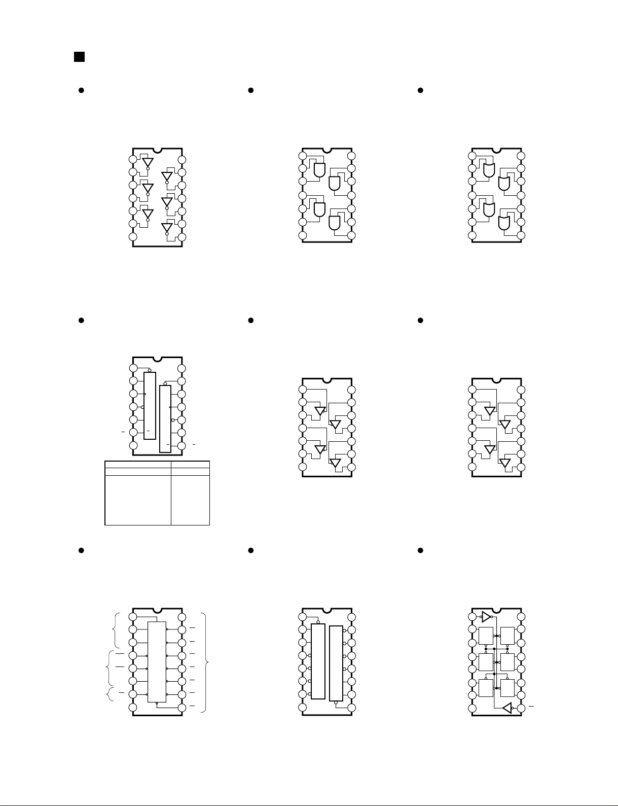
IC BLOCK DIAGRAM
SREV1
24
1
2
3
4
5
6
7
1A
1Y
2A
2Y
3A
3Y
Vss
14
13
12
11
10
9
8
VDD
6A
6Y
5A
5Y
4A
4Y
TC74VHC04F EL (XM332A00)
TC74VHCT04AF (XT777A00)
Hex Inverter
CPU: IC117, 133
TC74VHC08FT (XV891A00)
Quad 2 Input AND
CPU: IC301
TC74VHC32FT (XY945A00)
Quad 2 Input OR
CPU: IC121, 158
TC74VHC74FT (XV892A00)
Dual D-Type Flip-Flop
CPU: IC139
TC74VHC125FT (XY074A00)
Quad 3-State Bus Buffer
CPU: IC146
TC74VHCT126AFT (XY057A00)
Bus Buffer
CPU: IC145
TC74VHC138FT (XZ495A00)
3 to 8 Demultiplexer
CNV: IC19–22
TC74VHC139FT (XV893A00)
Dual 2 to 4 Demultiplexer
CPU:
CNV:
TC74ACT174F (XY938A00)
Hex D-Type Flip-Flop
CPU: IC163, 164
1
2
31A1Y
42A
52B
62Y
7
VSS
1B
14
13
12
VDD
4A
11 4Y
10 3B
93A
83Y
4B
1
2
31A1Y
42A
52B
62Y
7GND
1B
14
13
12
Vcc
4A
11 4Y
10 3B
93A
83Y
4B
INPUTS OUTPUTS
PR CLR CLK D Q Q
L
H
H
L
H
Q
O
H
L
H
H
L
Q O
X
X
X
H
L
X
X
X
X
f
f
L
H
L
L
H
H
H
L
H
L
H
H
H
1
2
3
4
5
6
7
1CLR
1D
1CK
1PR
1Q
1Q
GND
14
13
12
11
10
9
8
VCC
2CLR
CLR
2D
D
2CK
CK
2PRPR
2Q
2QQ
Q
CLR
D
CK
PR
Q
Q
1
2
3
4
5
6
7
1G
1A
2Y
2G
2A
2Y
GND
14
13
12
11
10
9
8
Vcc
4G
4A
4Y
3G
3A
3Y
1
2
3
4
5
6
7
1G
1A
1B
1Y0
1Y1
1Y2
1Y3
A
G
B
Y0
Y1
Y2
Y3
16
15
14
13
12
11
10
Vcc
2G
2A
2B
2Y0
2Y1
2Y2
8
GND
9
2Y3
Y2
Y3
Y1
Y0
B
A
G
1
2
3
4
5
6
7
A
A
Select
Enable
Output
Output
B
B
C
C
G2A
G2A
G2B
G2B
G1
G1
Y7
Y7 Y5
Y4
Y3
Y2
Y1
Y0
Y6
16
15
14
13
12
11
10
Vcc
YO
Y1
Y2
Y3
Y4
Y5
8
GND
9
Y6
Q
Q
DC K C K
C K
DC K
GG
CLEAR
1Q
1D
2D
2Q
3D
3Q
GND
1 16
2 15
3 14
4 13
5 12
6 11
7 10
8 9
Vcc
6Q
6D
5D
5Q
4D
4Q
CK
Q
D
GG
Q
DC K
G
C K
Q
D
G
Q
D
IC157, 169, 171
IC18
1
2
3
4
5
6
7
C1
A1
Y1
C2
A2
Y2
GND
14
13
12
11
10
9
8
Vcc
C4
A4
Y4
C3
A3
Y3
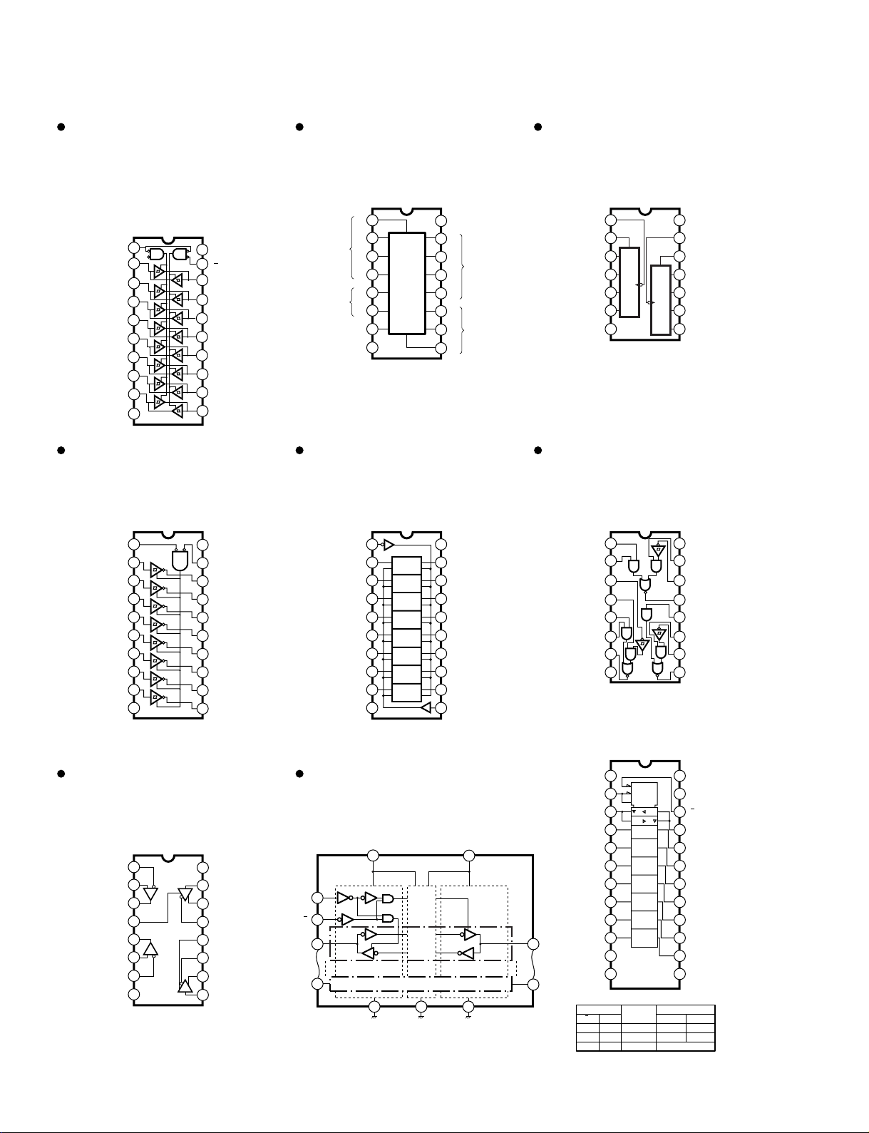
TC74VHCT245AFT (XT744A00)
TC74VHC245FT (XU797A00)
Octal 3-State Bus Transceiver
CPU:
CNV:
TC74HC251AF (XQ968A00)
3-State 8 to 1 Data Selector
CPU: IC160
HD74LV393AFPEL (IS039300)
Dual 4-Bit Binary Counter
CPU: IC302
HD74LVC540AT (XZ512A00)
Bus Buffer
CNV: IC17
TC74VHCT574AFT (XY059A00)
Octal D-Type Flip-Flop
CPU: IC161, 162
SN75124N (XE737A00)
Line Receiver
CPU: IC144
TC74LVXC3245FS (XY907A00)
Dual Supply Octal Bus Transceiver
CPU: IC127–131
SN75C1168NSR (XU073A00)
Line Driver/Receiver
CPU: IC125, 142
1
2
3
4
5
6
7
20
19
18
17
16
15
14
Vcc
G
B1
B2
B3
B4
B5
B6
B7
B8
8
9
10
12
11
GND
A8
A7
A6
A5
A4
A3
A2
A1
D1R
13
IC119, 120, 123, 155, 165–168, 170
172–174, 179–184
IC23–34
10
9
8
7
6
5
4
3
2
1
D5
D
CK
Q
OE
D
CK
Q
OE
D
CK
Q
OE
D
CK
Q
OE
D
CK
Q
OE
D
CK
Q
OE
D
CK
Q
OE
D
CK
Q
OE
D6
D7
GND
D4
D3
D2
D1
D0
Output
Control
Q5
Q6
Q7
Clock
Q4
Q3
Q2
Q1
Q0
Vcc
11
12
13
14
15
16
17
18
19
20
1
2
3
4
5
6
7
3
2
1
Y
W
STROBE
GND
0
16
15
14
13
12
11
Vcc
4
5
6
7
A
B
8
9
10
C
DATA
INPUTS
DATA
SELECT
DATE
INPUTS
OUTPUTS
D4
D5
B
C
S
D7
A
D6
D2 D3
D1
D0
Y
W
1
2
3
4
5
6
7
8
9
10
20
19
18
17
16
15
14
13
12
11
Vcc
GND
INPUTS
OUTPUTS
FUNCTION
G
L
L
H
DIR A-BUS B-BUS
L
H
X
A=B OUTPUT INPUT
B=A INPUT OUTPUT
Z High lmpedance
X : Don't Care
Z : High lmpedance
VCCA
DIR
A1
A2
A3
A4
A5
A6
A7
A8
GND
GND
V
CCB
NC
G
B1
1
3 EN2 (AB)
3 EN1 (BA)
G3
2
B2
B3
B4
B5
B6
B7
B8
GND
(TOP VIEW)
1
2
3
4
5
6
7
8
9
10
11
12
15
14
13
18
17
16
21
20
23
24
22
19
B1
21
V
CCA VCCB
B8
14
131211
1
2DIR
22G
10A8
3A1
Logic
Level
Converter
Same as above block
24
1A
1B
2R
2S
2A
2B
2Y
GND
1 16
2 15
3 14
4 13
5 12
6 11
7 10
8 9
Vcc
1S
1R
1Y
3A
3S
3R
3Y
1
2
3
4
5
6
7
1B
1A
1R
1DE
2R
2A
2B
16
15
14
13
12
11
10
Vcc
1D
1Y
1Z
2DE
2Z
2Y
8
GND
9
2D
1
2
3
4
5
6
7
1A
1 CLEAR
1QA
1QC
1QD
Vss
(GND)
1QB
14
13
12
11
10
9
VDD (Vcc)
2A
2 CLEAR
2QA
2QB
2QC
2QD
8
CL
QA
QB
QC
A
QD
CL
QA
QB
QC
A
QD
SREV1
25
SREV1
26
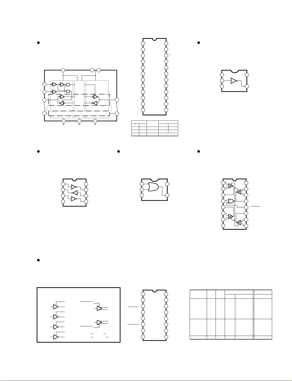
TC74LVX4245FS (XU229A00)
Dual Supply Octal Bus Transceiver
CPU: IC137, 138, 175–178
TC7S04F (XM182A00)
Inverter Gate
CPU: IC135
TC7W04FU (XP004A00)
Triple Inverter
CPU: IC152
TC7S32FU (XP351A00)
OR
CPU: IC136, 147
DS26C32ATMX (XU815A00)
Quad Differential Line Receiver
CPU: IC124
MC26LS30DR2 (XL334A00)
Line Driver
CPU: IC126
1
2
3
5
4
NC
VSS
VDD
OUT
IN
1
2
3
4
8
7
6
5
1A
GND
3Y
2A
Vcc
2Y
1Y
3A
INPUTS
OUTPUTS
FUNCTION
G
L
L
H
DIR A-BUS B-BUS
L
H
X
A=B OUTPUT INPUT
B=A INPUT OUTPUT
Z High lmpedance
X : Don't Care
Z : High lmpedance
VCCA
DIR
A1
A2
A3
A4
A5
A6
A7
A8
GND
GND
V
CCB
VCCB
G
B1
B2
B3
B4
B5
B6
B7
B8
GND
(TOP VIEW)
1
2
3
4
5
6
7
8
9
10
11
12
15
14
13
18
17
16
21
20
23
24
22
19
B1
21
23
V
CCA VCCB
24
B8
14
131211
1
2DIR
22G
10A8
3A1
Logic
Level
Converter
Same as above block
1 5
2
3
4
IN A
Vss
Vss
OUT
IN B
1
2
3
4
5
6
7
Vcc
Input A
Input B/
Enable AB
GND
Input C/
Enable CD
Input D
VEE
Mode
16
15
14
13
12
11
SR-A
Output A
Output B
SR-B
SR-C
Output C
Output D
8
9
10
SR-D
Input A
Enable AB
SR-A
Out A
2
3
15
14
Input A
2
16
15
Input B
SR-B
Out B
Out A
Out B
3
13
14
Input C
SR-C
Out C
6
12
11
Input D
SR-D
Out D
7
9
10
SINGLE-ENDED MODE
EIA-423
DIFFERENTIAL MODE
EIA-422
Enable CD
7
11
10
Input D
6
Out C
Out D
Vcc 1
Gnd 5
Mode 4VEE 8
Inputs Outputs
Operation Vcc Mode A B C D
X X X X
A B C D
Z Z Z Z
V
EE
0
0
0
0
0
0
1
1
1
1
1
0
1
X
1
0
1
0
1
0
0
0
0
0
1
0
0
0
0
0
1
0
0
0
1
1
0
1
X
0
0
0
0
1
0
0
0
0
0
1
0
0
0
1
0
0
1
Z
1
0
1
0
1
0
0
0
1
0
Z
0
1
0
0
0
1
0
0
0
1
1
0
1
Z
0
0
0
0
1
1
0
0
1
0
Z
0
0
0
1
0
+5.0 GND
+5.0 -5.0
Differential
(EIA-422-A)
Single-Ended
(EIA-423-A)
X = Don't Care
Z = High Impedance (Off)
X0XX
1
2
3
4
5
6
7
INPUT A
INPUT A
OUTPUT A
OUTPUT C
INPUT C
INPUT C
GND
ENABLE
16
15
14
13
12
11
Vcc
INPUT B
INPUT B
OUTPUT B
ENABLE
OUTPUT D
INPUT D
8
9
10
INPUT D
+
-
-
+
+
-
+
SREV1
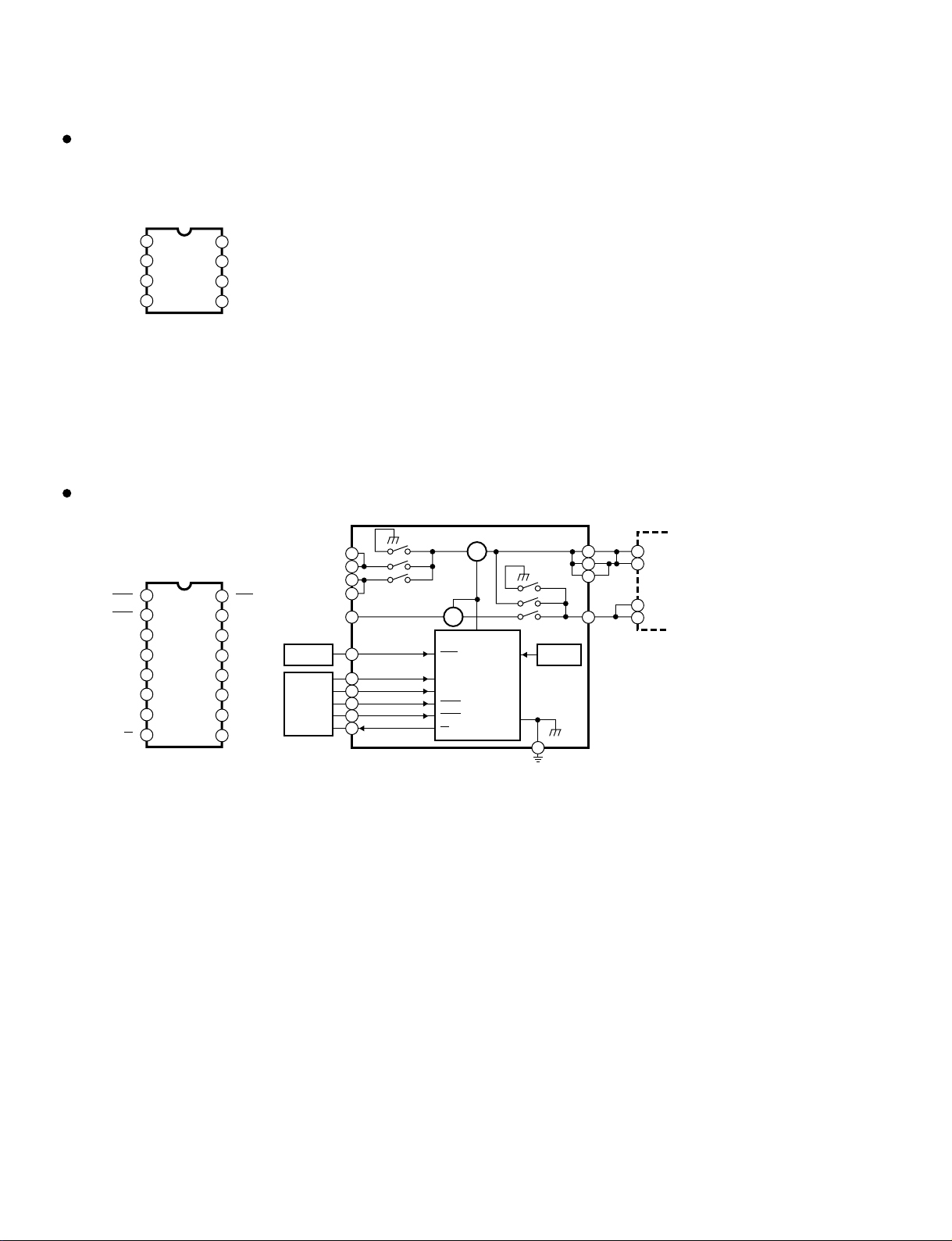
27
CY2305 (XY937A00)
Clock Buffer
CPU: IC110
TPS2211IDBR (XY906A00)
PCMCIA Power Interface Switch
CPU: IC132
1
2
3
4
5
6
7
VCCD0
VCCD1
3.3V
5V
5V
OC
GND
GND
3.3V
16
15
14
13
12
11
SHDN
VPPD0
VPPD1
VPPD0
VPPD1
AVCC
AVCC
AVCC
AVPP
8
9
10
12V
SHDN
VCCD0
VCCD1
OC
3.3V
3.3V
5V
5V
12V
CPU Thermal
S6
S5
S4
S3
S2
S1
Internal
Current Monitor
CONTROLLER
8
7
2
1
14
15
16
9
6
5
4
3
13 17
51
18
52
CS
TPS2211
CARD
Vcc1
Vcc2
Vpp1
Vpp2
CS
12
11
10
1
2
3
4
REF
CLK2
CLK1
GND
8
7
6
5
CLK OUT
CLK4
VDD
CLK3

SREV1
28
CIRCUIT BOARDS CONTENTS
Note: See parts list for details of circuit board component parts.
CD-ROM Circuit Board (XY898B0)·············································································· 34
CNV Circuit Board (XY897B0) ····················································································· 29
CPU Circuit Board (XY898B0) ····················································································· 33
PCM Circuit Board (XY898B0)····················································································· 37
SUB 1/4 Circuit Board (XY899B0) ··············································································· 38
SUB 2/4 Circuit Board (XY899B0) ··············································································· 39
SUB 3/4 Circuit Board (XY899B0) ··············································································· 40
SUB 4/4 Circuit Board (XY899B0) ··············································································· 40
 Loading...