

Yamaha PW-8 Service Manual
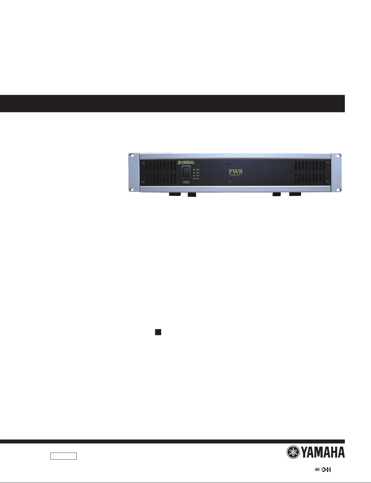
POWER SUPPLY
PW8
SERVICE MANUAL
PA
200807
011911
オープンプライス
CONTENTS(目次)
SPECIFICATIONS(総合仕様) .................................................3
DIMENSIONAL DIAGRAM(寸法図) ........................................3
PANEL LAYOUT(パネルレイアウト) ......................................4
CIRCUIT BOARD LAYOUT(ユニットレイアウト) .................5
DISASSEMBLY PROCEDURE(分解手順) ..............................6
IC BLOCK DIAGRAM(IC ブロック図) ..................................10
CIRCUIT BOARDS(シート基板図) .......................................10
PARTS LIST
BLOCK DIAGRAM(ブロックダイアグラム)
CIRCUIT DIAGRAM(回路図)
HAMAMATSU, JAPAN
Copyright (c) Yamaha Corporation. All rights reserved. PDF & ’08.07
PW8
IMPORTANT NOTICE
This manual has been provided for the use of authorized Yamaha Retailers and their service personnel. It has been assumed that basic
service procedures inherent to the industry, and more specifically Yamaha Products, are already known and understood by the users,
and have therefore not been restated.
WARNING : Failure to follow appropriate service and safety procedures when servicing this product may result in personal injury,
IMPORTANT : This presentation or sale of this manual to any individual or firm does not constitute authorization certification,
The data provided is belived to be accurate and applicable to the unit(s) indicated on the cover. The research engineering, and service
departments of Yamaha are continually striving to improve Yamaha products. Modifications are, therefore, inevitable and changes in
specification are subject to change without notice or obligation to retrofit. Should any discrepancy appear to exist, please contact the
distributor’s Service Division.
WARNING : Static discharges can destroy expensive components. Discharge any static electricity your body may have accumulated
destruction of expensive components and failure of the product to perform as specified. For these reasons, we advise
all Yamaha product owners that all service required should be performed by an authorized Yamaha Retailer or the
appointed service representative.
recognition of any applicable technical capabilities, or establish a principal-agent relationship of any form.
by grounding yourself to the ground bus in the unit (heavy gauge black wires connect to this bus.)
IMPORTANT : Turn the unit OFF during disassembly and parts replacement. Recheck all work before you apply power to the unit.
WARNING: This product contains chemicals known to the State of California to cause cancer, or birth defects or other reproductive harm.
DO NOT PLACE SOLDER, ELECTRICAL/ELECTRONIC OR PLASTIC COMPONENTS IN YOUR MOUTH FOR ANY REASON WHAT SO EVER!
Avoid prolonged, unprotected contact between solder and your skin! When soldering, do not inhale solder fumes or expose eyes to solder/
flux vapor!
If you come in contact with solder or components located inside the enclosure of this product, wash your hands before handling food.
IMPORTANT NOTICE FOR THE UNITED KINGDOM
Connecting the Plug and Cord
WARNING: THIS APPARATUS MUST BE EARTHED
IMPORTANT. The wires in this mains lead are coloured in accordance
with the following code:
GREEN-AND-YELLOW : EARTH
BLUE : NEUTRAL
BROWN : LIVE
As the colours of the wires in the mains lead of this apparatus may not
correspond with the coloured markings identifying the terminals in
your plug proceed as follows:
The wire which is coloured GREEN-and-YELLOW must be connected to
the terminal in the plug which is marked by the letter E or by the safety
earth symbol
The wire which is coloured BLUE must be connected to the terminal
which is marked with the letter N or coloured BLACK.
The wire which is coloured BROWN must be connected to the terminal
which is marked with the letter L or coloured RED.
• This applies only to products distributed by Yamaha Music U.K. Ltd. (3 wires)
or colored GREEN or GREEN-and-YELLOW.
WARNING
Components having special characteristics are marked and must be replaced with parts having specifi cation equal to those
originally installed.
2
印の部品は、安全を維持するために重要な部品です。交換する場合は、安全のために必ず指定の部品をご使用ください。
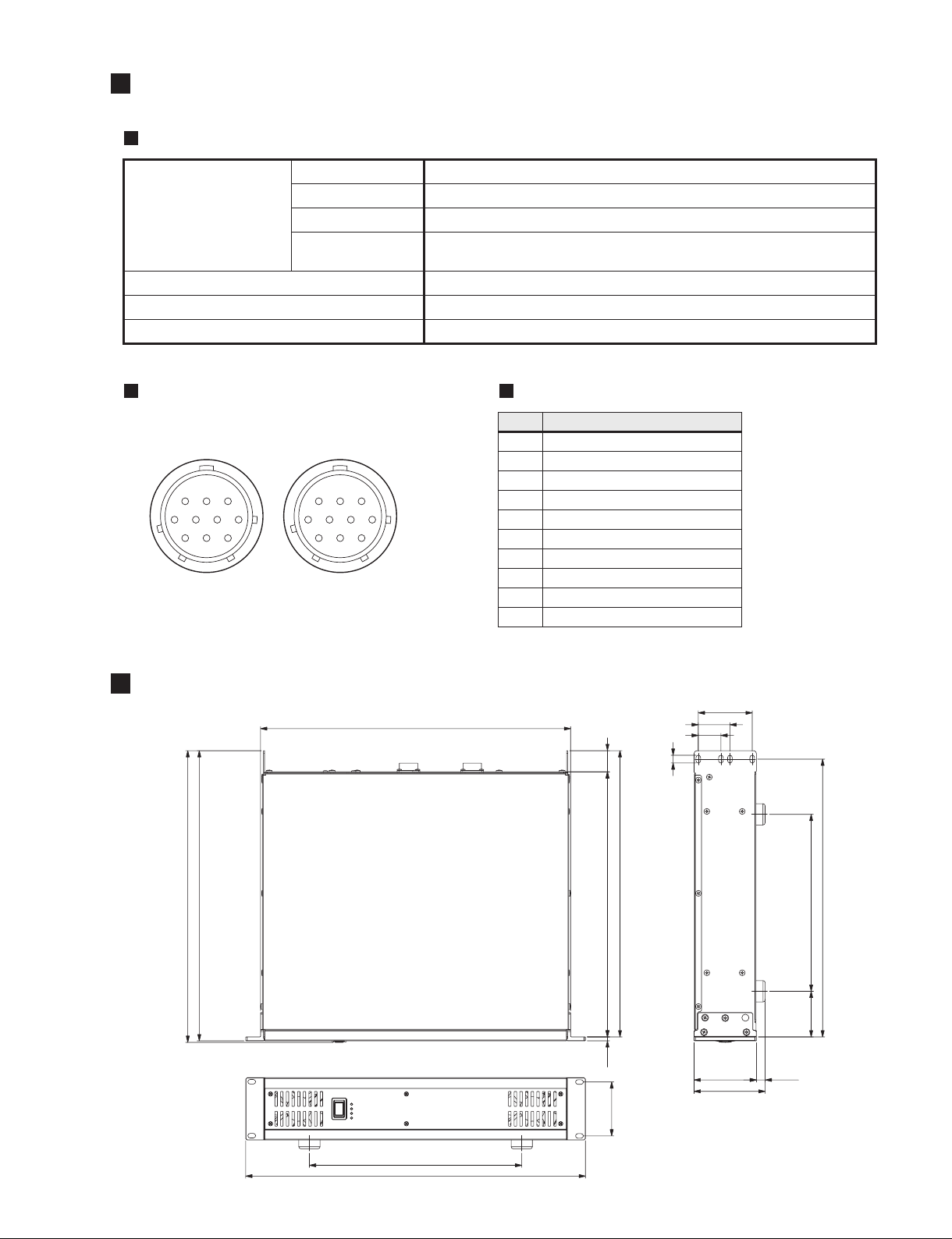
SPECIFICATIONS(総合仕様)
General Specifications
+15V Green LED: On (+15 V), Off (less than +10 V or more than +21 V)
-15V Green LED: On (-15 V), Off (less than -21 V or more than -10 V)
Secondary Voltage
Power Consumption 265 W (IM8-40), 230 W (IM8-32), 200 W (IM8-24)
Dimensions Height: 100.5 mm, Depth: 412 mm, Width: 480 mm
Net Weight 11 kg
Power Connector Pin Diagram Power Supply Cable Pin Assignments
+12V Green LED: On (+12 V), Off (less than +7.6 V or more than +18 V)
+48V
(Phantom Voltage)
Green LED: On (+48 V), Off (less than +32 V)
PW8
DC PARALLEL INPUT
DC OUTPUT
1 Power supply remote
2 +15 V
No. Function
123
5467
8910
321
6754
1098
3 ±15 V GND
4 +48 V GND
5 -15 V
6 +12 V
7 +12 V GND/power supply remote
8 Power supply remote
9 +48 V
10 FRAME GND
DIMENSIONAL DIAGRAM(寸法図)
438
76.2
44.7
32
30
11
410
D: 412
300
W: 480
374.5
5.5
76.2
404.5
88 12.5
H: 100.5
Units: mm
392.5
64.5 250
3
PW8
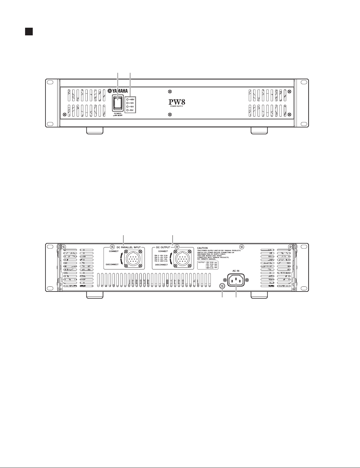
PANEL LAYOUT(パネルレイアウト)
Front Panel(フロントパネル)
/4
q POWER Switch
w Operation Monitor
(+48V, +12V, +15V, -15V)
Rear Panel(リアパネル)
q DC PARALLEL INPUT Connector
w DC OUTPUT Connector
e AC IN Connector
r Ground Screw Terminal
q POWERスイッチ
w オペレーションモニター
(+48V、+12V、+15V、-15V)
/4
)0
q DCPARALLELINPUT端子
w DCOUTPUT端子
e ACIN端子
r アース用ネジ
4
CIRCUIT BOARD LAYOUT(ユニットレイアウト)
PW8
<TOP VIEW>
DC ASSEMBLY (L)
(DCAssy(L))
AC1
DC1DC2
DC ASSEMBLY (R)
(DCAssy(R))
<FRONT VIEW>
AC2AC3
FRONT PANEL 1(フロントパネル1)
5
PW8
DISASSEMBLY PROCEDURE(分解手順)
The par ts marked “※” are power transformer
components.
(※は電源トランスの構成部品です。)
WASHER
(ワッシャー)
PLATE B
(プレートB)
RUBBER S
(ゴムS)
RUBBER L
(ゴムL)
DC ASSEMBLY (L)
(DCASSY(L))
FAN (L)
(DC ファン(L))
AC3
[40] x 2
[140] x 3
A
HEXAGONAL NUT A
※
[50]
[160B] x 4
(六角ナットA)
SHIELD BOARD
(シールド板)
※
PLATE A
(プレートA)
HEXAGONAL NUT B
※
(六角ナットB)
[300] x 6
※
[470] x 3
AC WIRING ASSEMBLY
(AC 束線)
[380C]
AC1
EARTH CABLE C
(アース線C)
[470]
x 5
[380B]
[380A]
[400]
EARTH CABLE B
(アース線B)
EARTH CABLE A
(アース線A)
PS WIRING ASSEMBLY(OUTPUT)
(PS 束線(OUTPUT))
PS WIRING ASSEMBLY
[370]
(DC PARALLEL INPUT)
x 4
x 2
(PS 束線(DCPARALLELINPUT))
[350]
x 4
TOP COVER
(トップカバー)
[470] x 3
FRONT PANEL 1
(フロントパネル1)
POWER SWITCH KNOB
(PSWノブ)
6
AC2
[120] x 2
[240] x 6
[80] x 2
FRONT PANEL 2
(フロントパネル2 )
[140] x 3
[40] x 2
※
MAIN CHASSIS ASSEMBLY
(メインシャーシAS SY)
HEXAGON HEAD BOLT
(六角ボルト)
PS WIRING ASSEMBLY
(DC PARALLEL INPUT)
(PS 束線(DCPARALLELINPUT))
[40]: BIND HEAD SCREW(小ネジ+BIND)4.0X16 MFZN2W3 SP (WE98400R)
[50]: HEXAGONAL NUT(ナット 6角)M4 #1 (WG169200)
[80]: BIND HEAD TAPPING SCREW-S(Sタイト+BIND)3.0X5 MFZN2W3 (WE98020R)
[120]: BIND HEAD TAPPING SCREW-S(Sタイト+BIND)3.0X5 MFZN2W3 (WE98020R)
[140]: BIND HEAD TAPPING SCREW-B(Bタイト+BIND)4.0X8 MFZN2B3 (WE962000)
[160]: BIND HEAD TAPPING SCREW-B(Bタイト+BIND)4.0X8 MFZN2B3 (WE962000)
[240]: BIND HEAD TAPPING SCREW-S(Sタイト+BIND)3.0X8 MFZN2B3 (WF25750R)
[300]: BIND HEAD TAPPING SCREW-S(Sタイト+BIND)3.0X5 MFZN2W3 (WE98020R)
[350]: BIND HEAD TAPPING SCREW-B(Bタイト+BIND)3.0X10 MFZN2B3 (WE972200)
[370]: BIND HEAD TAPPING SCREW-B(Bタイト+BIND)3.0X10 MFZN2B3 (WE972200)
[380]: BIND HEAD TAPPING SCREW-S(Sタイト+BIND)4.0X6 MFZN2B3 (WE974300)
[400]: BIND HEAD TAPPING SCREW-B(Bタイト+BIND)3.0X10 MFZN2B3 (WE972200)
[470]: BIND HEAD TAPPING SCREW-B(Bタイト+BIND)4.0X8 MFZN2B3 (WE962000)
Fig. 1
(図1)
[160A] x 4
[50]
(DC ファン(R))
<REAR VIEW >
[470]
FAN (R)
PS WIRING ASSEMBLY(OUTPUT)
(PS 束線(OUTPUT))
[350]
DC ASSEMBLY (R)
(DCASSY(R))
AC WIRING ASSEMBLY
[370]
(AC 束線)
[470]
[400]
PW8
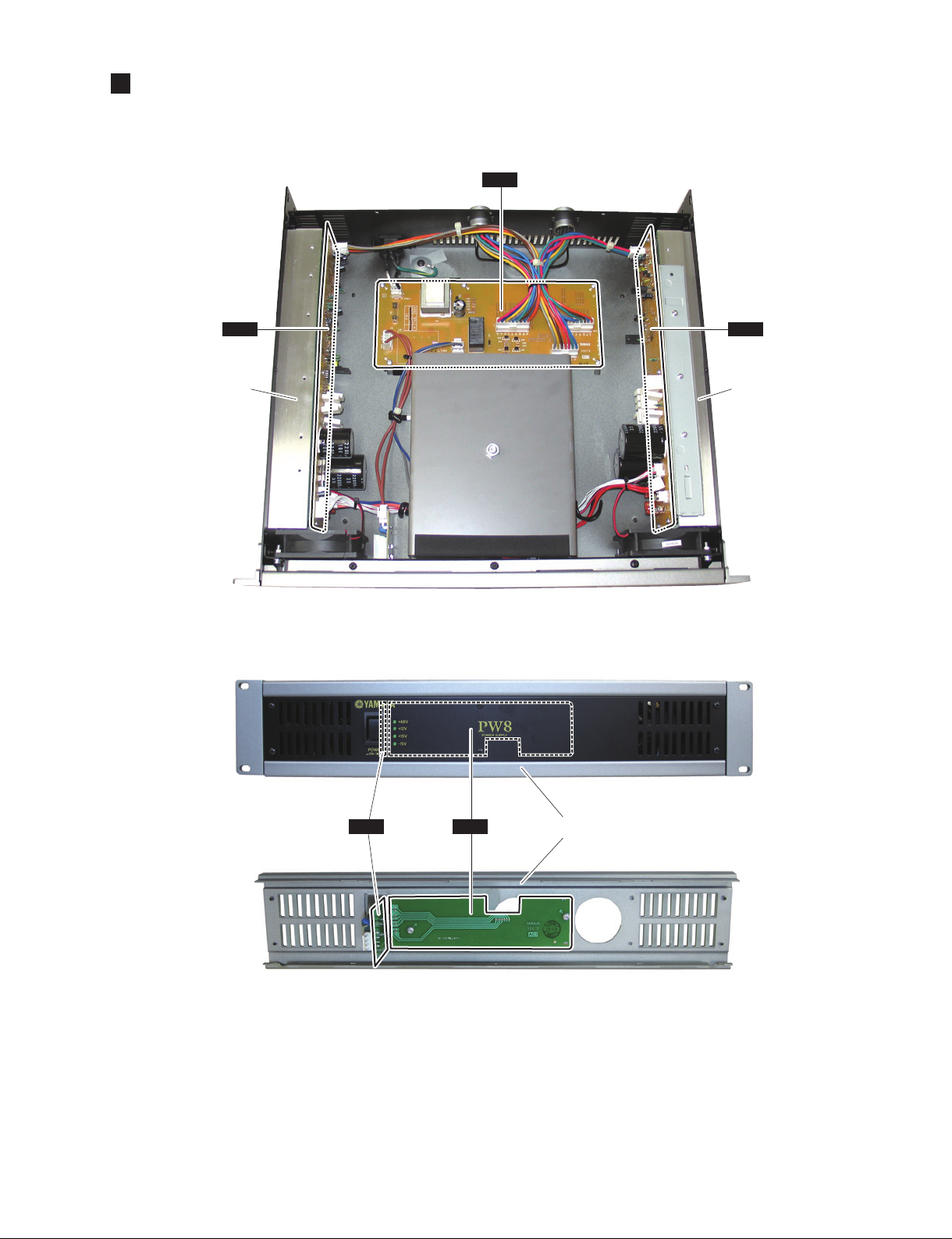
1. Top Cover (Time required: About 2 minutes)
Remove the eleven (11) screws marked [470]. The top
cover can then be removed. (Fig. 1)
2. Power Transformer
(Time required: About 3 minutes)
2-1 Remove the top cover. (See procedure 1.)
2-2 Remove the hexagonal nut A. The shield board and
plate A can then be removed. (Fig. 1)
2-3 Remove the hexagonal nut B and remove the hexagon
bolt from the bottom side of the main chassis assembly.
The parts marked "A" can then be removed. (Fig. 1)
3. DC Assembly
3-1 Remove the top cover. (See procedure 1.)
3-2 DC1 Circuit Board
(Time required: About 5 minutes)
3-2-1 Remove the four (4) screws marked [160A]. The DC
assembly (R) can then be removed. (Fig. 1)
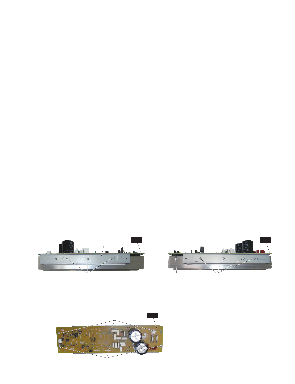
3-2-2 Remove the three (3) screws marked [R70A]. The
transistor fi xing plate A can then be removed. (Photo 1)
3-2-3 Remove the four (4) screws marked [R70B]. The
transistor fi xing plate B can then be removed. (Photo 2)
3-2-4 Remove the six (6) screws marked [R40] and the screw
marked [R70C]. The DC1 circuit board can then be
removed. (Photo 2, Photo 3)
* The diode stack and transistor of the DC1 circuit
board are in close contact with the insulation sheet.
(Photo 4, Photo 5)
1. トップカバー
(所要時間:約 2 分)
[470] のネジ 11 本を外し、トップカバーを外しま
す。(図 1)
2. 電源トランス
(所要時間:約 3 分)
2-1 トップカバーを外します。(1 項参照 )
2-2 六角ナット A を外し、シールド板とプレート A を
外します。(図 1)
2-3 六角ナット B と、メインシャーシ Ass'y の底面側
から六角ボルトを外し、図 1 の A の部分を外しま
す。(図 1)
3. DC 電源セット
3-1 トップカバーを外します。(1 項参照 )
3-2 DC1 シート(所要時間:約 5 分)
3-2-1 [160A] のネジ 4 本を外し、DCAss'yR を外します。
(図 1)
3-2-2 [R70A] のネジ 3 本を外し、TR 押え金具 A を外し
ます。(写真 1)
3-2-3 [R70B] のネジ 4 本を外し、TR 押え金具 B を外し
ます。(写真 2)
3-2-4 [R40] の ネ ジ 6 本 と [R70C] の ネ ジ 1 本 を 外 し、
DC1 シートを外します。(写真 2、写真 3)
※ DC1 シートのダイオードスタックおよびトランジスタ
は放熱シートに密着しています。(写真 4、写真 5)
• DC ASSEMBLY (R)(DCASSY(R))
<TOP VIEW>
TRANSISTOR FIXING PLATE A
(TR 押え金具 A)
[R70A]
[R70A]: BIND HEAD SCREW(小ネジ+BIND)
3.0X10 MFZN2W3 (WE95290R)
Photo 1
(写真1)
• DC ASSEMBLY (R)(DCASSY(R))
<LEFT SIDE VIEW>
[R40]
[R40]
DC1
Photo 3
DC1
(写真3)
• DC ASSEMBLY (R)(DCASSY(R))
<LOWER VIEW>
[R70]: BIND HEAD SCREW(小ネジ+BIND)
3.0X10 MFZN2W3 (WE95290R)
[R40]: BIND HEAD SCREW(小ネジ+BIND)
3.0X6 MFZN2W3 (WE774000)
TRANSISTOR FIXING PLATE B
(TR 押え金具 B)
[R70B][R70C]
Photo 2
(写真2)
DC1
7
PW8
• DC ASSEMBLY (R)(DCASSY(R))
<TOP VIEW>
DIODE STACK and TRANSISTOR
(ダイオードスタックとトランジスタ)
Photo 4
INSULATION SHEET
(放熱シ−ト)
(写真4)
DC1
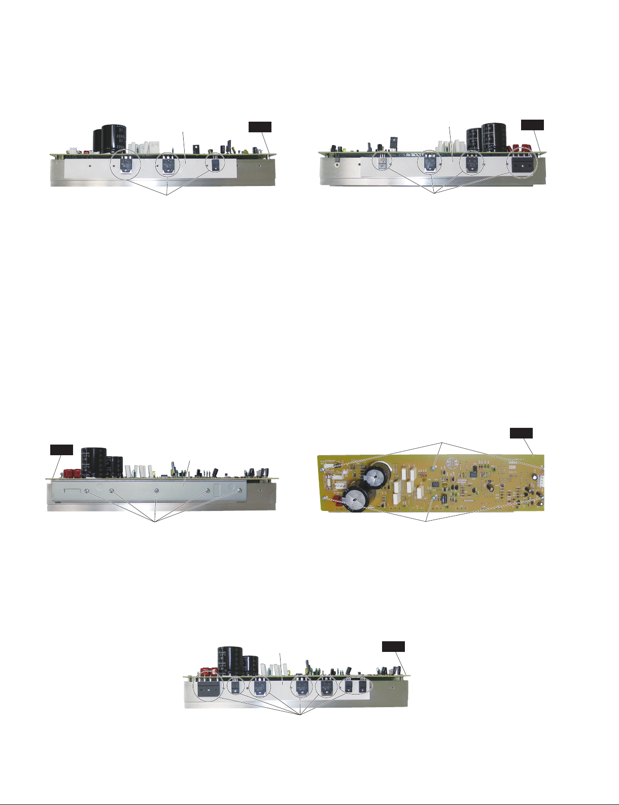
3-3 DC2 Circuit Board
(Time required: About 5 minutes)
3-3-1 Remove the four (4) screws marked [160B]. The DC
assembly (L) can then be removed. (Fig. 1)
3-3-2 Remove the five (5) screws marked [L70]. The
transistor fi xing plate C can then be removed. (Photo 6)
3-3-3 Remove the six (6) screws marked [L40]. The DC2
circuit board can then be removed. (Photo 7)
* The diode stack and transistor of the DC2 circuit
board are in close contact with the insulation sheet.
(Photo 8)
• DC ASSEMBLY (R)(DCASSY(R))
<LOWER VIEW>
DIODE STACK and TRANSISTOR
(ダイオードスタックとトランジスタ)
INSULATION SHEET
(放熱シ−ト)
Photo 5
(写真5)
DC1
3-3 DC2 シート(所要時間:約 5 分)
3-3-1 [160B] のネジ 4 本を外し、DCAss'yL を外します。
(図 1)
3-3-2 [L70] のネジ 5 本を外し、TR 押え金具 C を外しま
す。(写真 6)
3-3-3 [L40] のネジ 6 本を外し、DC2 シートを外します。
(写真 7)
※ DC2 シートのダイオードスタックおよびトランジスタ
は放熱シートに密着しています。(写真 8)
• DC ASSEMBLY (L)(DCASSY(L))
<LOWER VIEW>
DC2
[L70]: BIND HEAD SCREW(小ネジ+BIND)
3.0X10 MFZN2W3 (WE95290R)
TRANSISTOR FIXING PLATE C
(TR 押え金具 C)
[L70]
Photo 6
(写真6)
• DC ASSEMBLY (L)(DCASSY(L))
<LOWER VIEW>
INSULATION SHEET
(放熱シ−ト)
• DC ASSEMBLY (L)(DCASSY(L))
<RIGHT SIDE VIEW>
[L40]: BIND HEAD SCREW(小ネジ+BIND)
3.0X6 MFZN2W3 (WE774000)
Photo7
[L40]
[L40]
(写真7)
DC2
DC2
DIODE STACK and TRANSISTOR
(ダイオードスタックとトランジスタ)
Photo 8
(写真8)
8

PW8
4. AC1 Circuit Board
(Time required: About 3 minutes)
4-1 Remove the top cover. (See procedure 1.)
4-2 Remove the six (6) screws marked [300]. The AC1
circuit board can then be removed. (Fig. 1)
5. PS Wiring Assembly
5-1 Remove the top cover. (See procedure 1.)
5-2 DC PARALLEL INPUT
(Time required: About 3 minutes)
5-2-1 Remove the screw marked [380A]. The earth cable A
can then be removed. (Fig. 1)
5-2-2 Remove the four (4) screws marked [350]. The DC
wiring assembly (DC PARALLEL INPUT) can then be
removed. (Fig. 1)
5-3 DC OUTPUT (Time required: About 3 minutes)
5-3-1 Remove the screw marked [380B]. The earth cable B
can then be removed. (Fig. 1)
Remove the four (4) screws marked [370]. The DC wiring
5-3-2
assembly (OUTPUT) can then be removed. (Fig. 1)
6. AC Wiring Assembly
(Time required: About 3 minutes)
6-1 Remove the top cover. (See procedure 1.)
6-2 Remove the screw marked [380C]. The earth cable C
can then be removed. (Fig. 1)
6-3 Remove the two (2) screws marked [400]. The AC
wiring assembly can then be removed. (Fig. 1)
4. AC1 シート
4-1 トップカバーを外します。(1 項参照 )
4-2 [300] のネジ 6 本を外し、AC1 シートを外します。
(図 1)
(所要時間:約 3 分)
5. PS 束線
5-1 トップカバーを外します。(1 項参照 )
5-2 DCPARALLELINPUT(所要時間:約 3 分)
5-2-1 [380A] のネジ 1 本を外し、アース線 A を外します。
(図1)
5-2-2 [350] の ネ ジ 4 本 を 外 し、DC 束 線(DCPARAL-
LELINPUT)を外します。(図 1)
5-3 DCOUTPUT(所要時間:約 3 分)
5-3-1 [380B] のネジ 1 本を外し、アース線 B を外します。
(図1)
5-3-2 [370] のネジ 4 本を外し、DC 束線(OUTPUT)を
外します。(図 1)
6. AC 束線
6-1 トップカバーを外します。(1 項参照 )
6-2 [380C] のネジ 1 本を外し、アース線 C を外します。
(図1)
6-3 [400] のネジ 2 本を外し、AC 束線を外します。(図 1)
(所要時間:約 3 分)
7. AC3 Circuit Board
(Time required: About 4 minutes)
7-1 Remove the top cover. (See procedure 1.)
7-2 Remove the six (6) screws marked [240]. The front
panel 2 can then be removed. (Fig. 1)
7-3 Remove the power switch knob from the AC3 circuit
board. (Fig. 1)
7-4 Remove the two (2) screws marked [80]. The AC3
circuit board can then be removed. (Fig. 1)
8. AC2 Circuit Board
(Time required: About 4 minutes)
8-1 Remove the top cover. (See procedure 1.)
8-2 Remove the six (6) screws marked [140]. The front
panel 1 can then be removed. (Fig. 1)
8-3 Remove the two (2) screws marked [120]. The AC2
circuit board can then be removed. (Fig. 1)
9. Fan (L,R) (Time required: About 5 minutes)
9-1 Remove the top cover. (See procedure 1.)
9-2 Remove the six (6) screws marked [140]. The front
panel 1 can then be removed. (Fig. 1)
9-3 Remove the two (2) screws marked [40] and two (2)
hexagonal nuts marked [50]. The fan (L) can then be
removed. (Fig. 1)
* The fan (R) can be removed in the same way.
7. AC3 シート
7-1 トップカバーを外します。(1 項参照 )
7-2 [240] のネジ 6 本を外し、フロントパネル 2 を外
します。(図 1)
7-3 PSW ノブを AC3 シートから外します。(図 1)
7-4 [80] のネジ 2 本を外し、AC3 シートを外します。
(図1)
8. AC2 シート
8-1 トップカバーを外します。(1 項参照 )
8-2 [140] のネジ 6 本を外し、フロントパネル 1 を外
します。(図 1)
8-3 [120] のネジ 2 本を外し、AC2 シートを外します。
(図 1)
9. DC ファン(L・R)
9-1 トップカバーを外します。(1 項参照 )
9-2 [140] のネジ 6 本を外し、フロントパネル 1 を外
します。(図 1)
9-3 [40] のネジ 2 本と [50] の六角ナット 2 個を外し、
DC ファン (L) を外します。(図 1)
※ DC ファン (R) も同じ手順で外せます。
(所要時間:約 4 分)
(所要時間:約 4 分)
(所要時間:約 5 分)
9
PW8
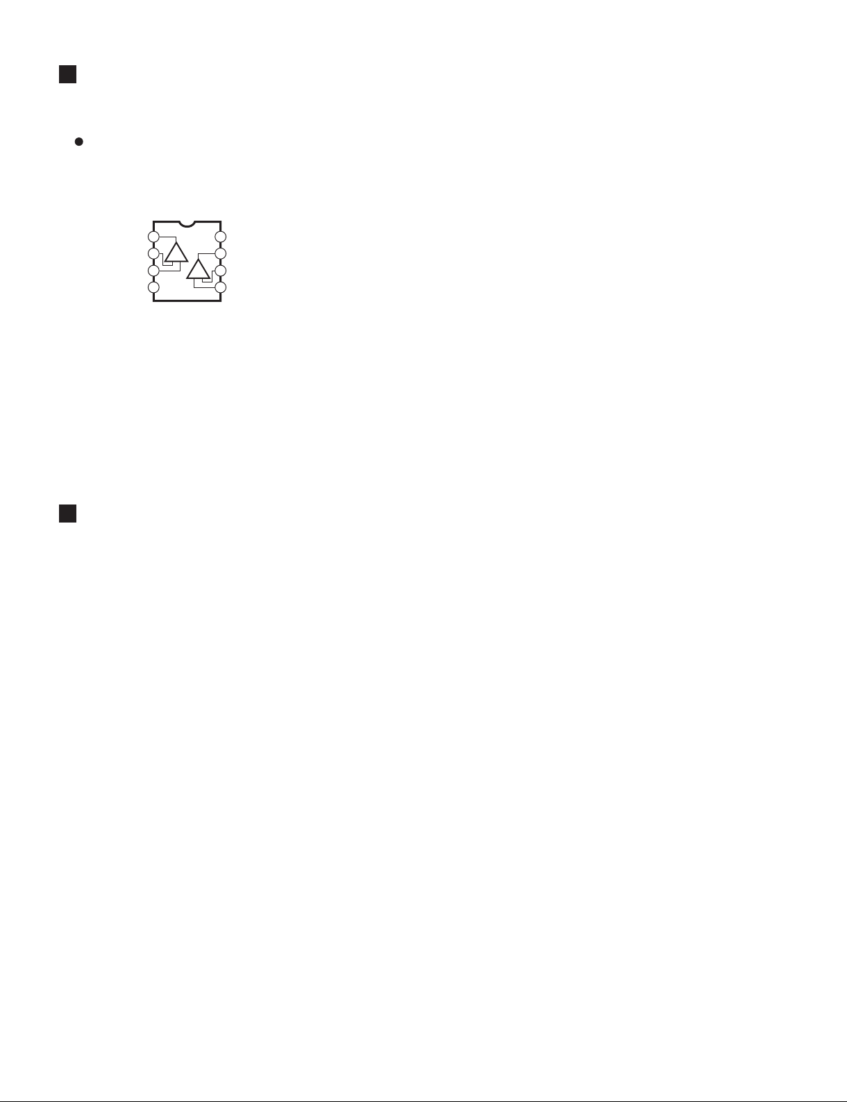
IC BLOCK DIAGRAM(IC ブロック図)
μPC4570C (XC520A00)
DC1: IC101
DC2: IC201, IC202
Dual Operational Amplifier
+-
+DC Voltage
8
Supply
7
Output B
Inverting
6
Input B
Non-Inverting
5
Input B
Output A +V
Inverting
Input A
Non-Inverting
Input A
-DC Voltage Supply
1
2
3
4-V
+-
CIRCUIT BOARDS(シート基板図)
AC1 Circuit Board (X8678C0) ..............................................................11
AC2 Circuit Board (X8678C0) ............................................................. 12
AC3 Circuit Board (X8678C0) ............................................................. 12
DC1 Circuit Board (X8679D0) ............................................................. 13
DC2 Circuit Board (X8679D0) ............................................................. 14
10
Note: See parts list for details of circuit board component parts.
注 : シートの部品詳細はパーツリストをご参照ください。
 Loading...