Page 1
YMF715E
OPL3-SA3
Preliminary
OPL3 Single-chip Audio System 3
OUTLINE
■■■■
YMF715E-S (OPL3-SA3) is a single audio chip that integrates OPL3 and its DAC, 16bit Sigma-delta
CODEC, MPU401 MIDI interface, joystick port, and a 3D enhanced controller including all the analog
components which is suitable for multi-media application. This LSI is fully compliant with Plug and Play
ISA 1.0a, and supports all the necessary features, i.e. 16bit address decode, more IRQs and DMAs in
compliance with PC’96. This LSI also supports the expandability, i.e. Zoomed Video, Modem and CDROM interface in a Plug and Play manner, and power management (power down, power save, partial
power down, and suspend/resume) that is indispensable with power-conscious application.
FEATURES
■■■■
Built-in OPL3 (FM-synthesizer)
●
Supports Sound Blaster Game compatibility
●
Supports Windows Sound System compatibility
●
Supports Plug & Play ISA 1.0a compatibility
●
Full Duplex operation
●
Built-in MPU401 Compatible MIDI I/O port
●
Built-in Joystick port
●
Built-in the 3D enhanced controller including all the analog components
●
Supports multi-purpose pin function
●
(Support 16-bit address decode, DAC interface for OPL4-ML/ML2, Zoomed Video port, EEPROM
interface, MODEM interface, IDE CD-ROM interface)
Hardware and software master volume control
●
Supports monaural input
●
24 mA TTL bus drive capability
●
Supports Power Management(power down, power save, partial power down, and suspend/resume)
●
+5V/ +3.3V power supply for digital, 5V power supply for analog.
●
100 pin SQFP package (YMF715E-S)
●
The contents of this catalog are target specifications and are subject to change
without prior notice. When using this device, please recheck the specifications.
YAMAHA
CORPORATION
May 21, 1997
Page 2
YMF715E
/
/
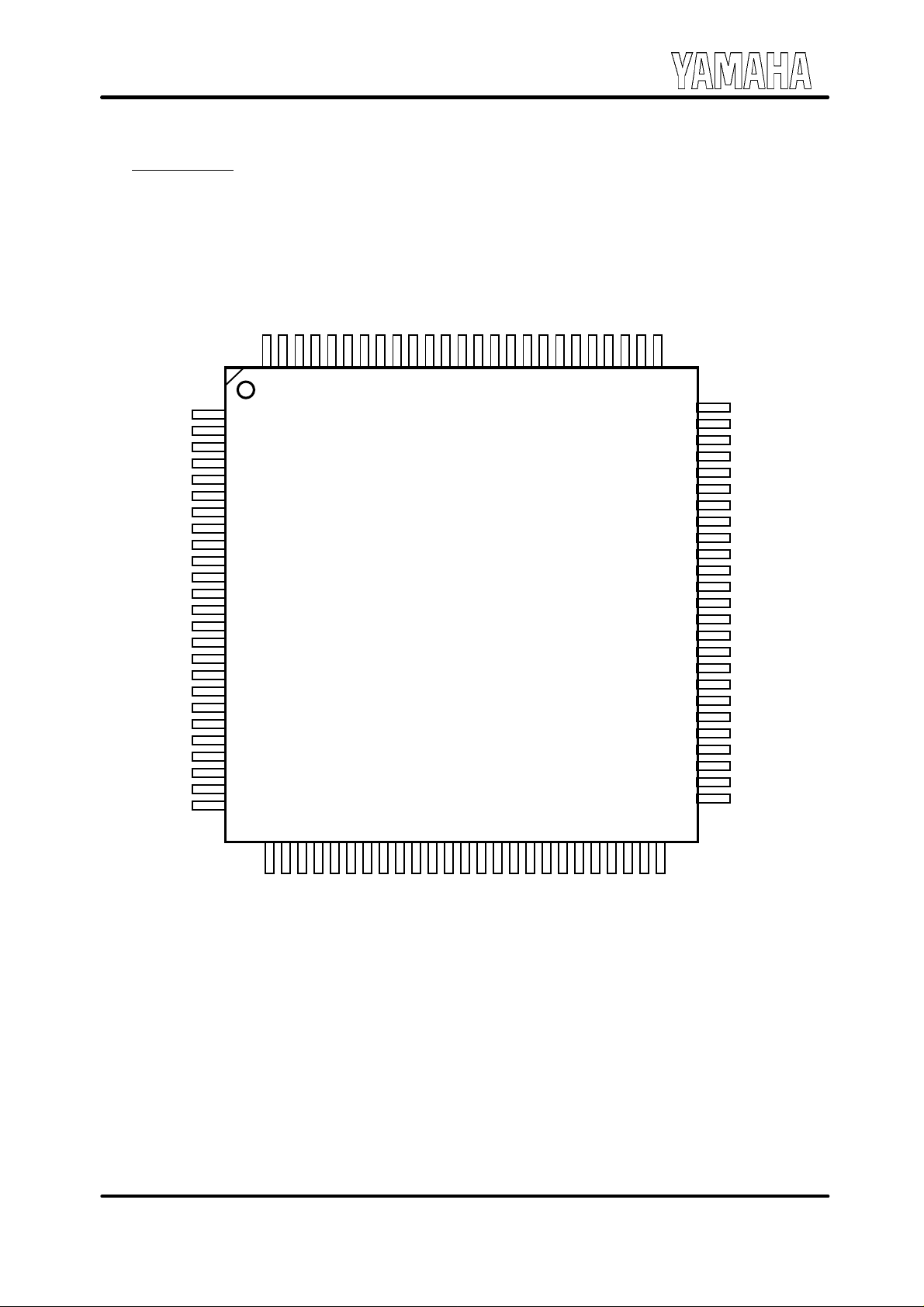
PIN CONFIGURATION
■■■■
YMF715E-S
SBFLTR
SBFLTL
SYNSHL
SYNSHR
TRECR
TRECL
AUX2L
AUX2R
MIC
MIN
VREFO
VREFI
AVSS
AVDD
LINEL
LINER
AUX1L
AUX1R
OUTL
OUTR
VOCIL
VOCIR
VOCOR
VOCOL
ADFLTL
AVSS
AVDD
GP0
GP1
GP2
GP3
GP4
GP5
GP6
GP7
DVSS
RESET
/IOW
/IOR
DVDD
AEN
A11
A10
A9
IRQ3
IRQ5
IRQ7
IRQ9
IRQ10
IRQ11
9998979695949392919089888786858483828180797877
100
1
2
3
4
5
6
7
8
9
10
11
12
13
14
15
16
17
18
19
20
21
22
23
24
25
26272829303132333435363738394041424344454647484950
76
75
74
73
72
71
70
69
68
67
66
65
64
63
62
61
60
59
58
57
56
55
54
53
52
51
ADFLTR
DVSS
SEL0
SEL1
SEL2
MP0
MP1
MP2
MP3
MP4
MP5
MP6
MP7
MP8
MP9
DVDD
VOLUP
VOLDW
A0
A1
A2
X33O
X33I
X24O
X24I
D0D1D2
DRQ0
DRQ1
/DACK0
DRQ3
/DACK1
/DACK3
D3
DVSS
DVDD
D4D5D6
100 pin SQFP Top View
A8A7A6A5A4
D7
A3
RXD
DVSS
TXD
May 21, 1997
-2-
Page 3
YMF715E
p
p
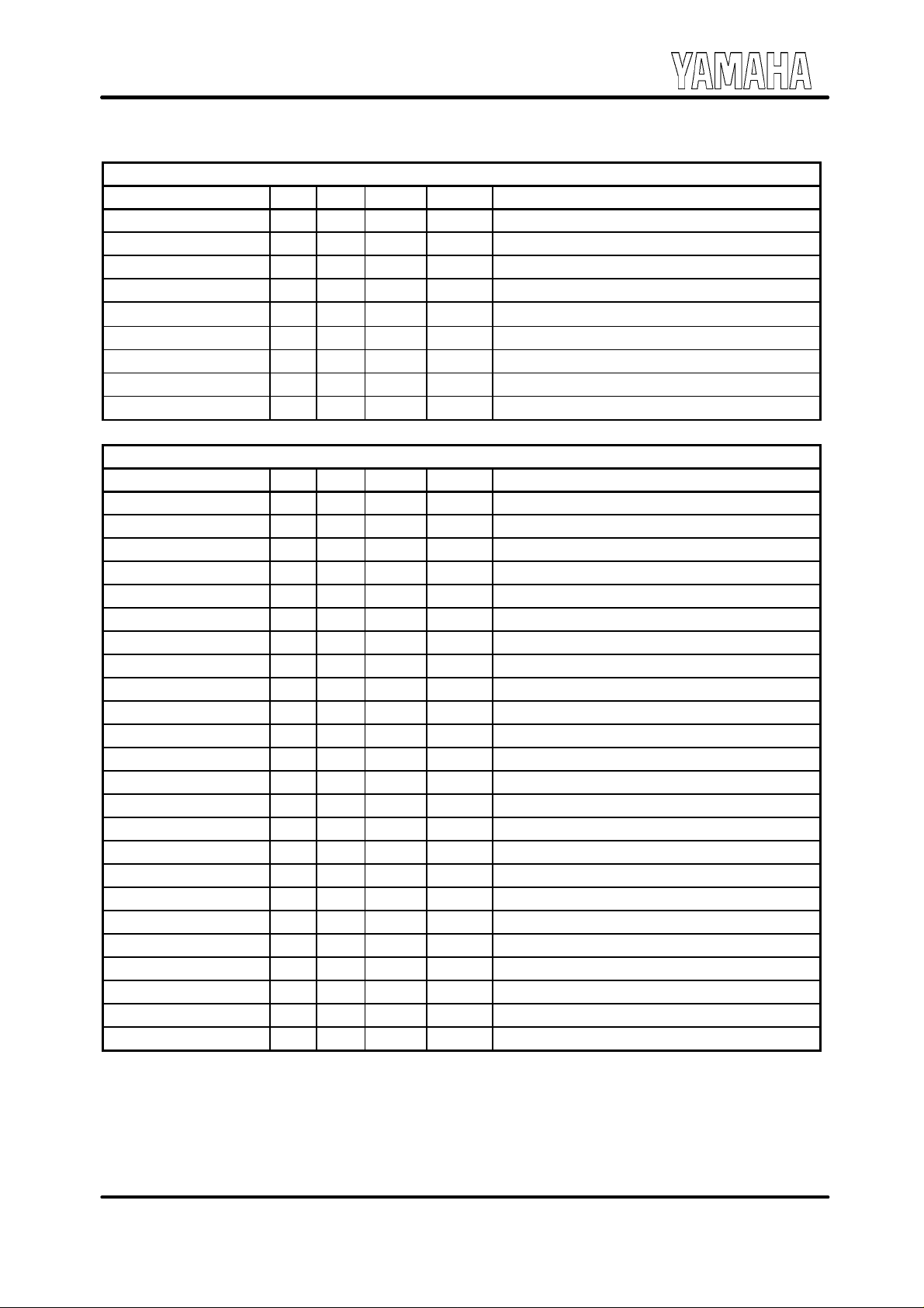
PIN DESCRIPTION
■
ISA bus interface: 36 pins
name
D7-0 8 I/O TTL 24mA Data Bus
A11-0 12 I TTL - Address Bus
AEN 1 I TTL - Address Bus Enable
/IOW 1 I
/IOR 1 I
RESET 1 I
IRQ3,5,7,9,10,11 6 T TTL 12mA Interrupt request
DRQ0, 1, 3 3 T TTL 12mA DMA Request
/DACK0, 1, 3 3 I TTL - DMA Acknowledge
Analog Input & Output : 24 pins
name
OUTL 1 O - - Left mixed analog output
OUTR 1 O - - Right mixed analog output
VREFI 1 I - - Voltage reference input
VREFO 1 O - - Voltage reference output
AUX1L 1 I - - Left AUX1 input
AUX1R 1 I - - Right AUX1 input
AUX2L 1 I - - Left AUX2 input
AUX2R 1 I - - Right AUX2 input
LINEL 1 I - - Left LINE input
LINER 1 I - - Right LINE input
MIC 1 I - - MIC input
MIN 1 I - - Monaural input
TRECL 1 - - - Left Treble capacitor
TRECR 1 - - - Right Treble capacitor
SBFLTL 1 - - - Left SBDAC filter
SBFLTR 1 - - - Right SBDAC filter
SYNSHL 1 - - - Left SYNDAC sample / hold capacitor
SYNSHR 1 - - - Right SYNDAC sample / hold capacitor
ADFLTL 1 - - - Left input filter
ADFLTR 1 - - - Right input filter
VOCOL 1 O - - Left voice output
VOCOR 1 O - - Right voice output
VOCIL 1 I - - Left voice input
VOCIR 1 I - - Right voice input
ins I/O type Size function
Schmitt
Schmitt
Schmitt
ins I/O type size function
- Write Enable
- Read Enable
- Reset
May 21, 1997
-3-
Page 4
YMF715E
p
p
)
)
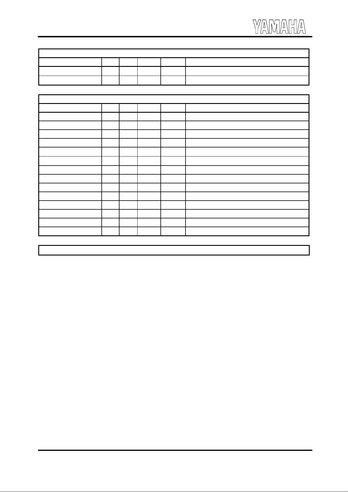
Multi-purpose pins : 13 pins
name
SEL2-0 3 I+ CMOS - Refer to “Multi-purpose pins” section
MP9-0 10 I+/O TTL 2mA Refer to “multi-purpose pins” section
Others : 27 pins
name
GP3-0 4 IA - - Game Port
GP7-4 4 I+
RXD 1 I+
TXD 1 O TTL 4mA MIDI Data Transfer
/VOLUP 1 I+
/VOLDW 1 I+
X33I 1 I CMOS - 33.8688 MHz
X33O 1 O CMOS 2mA 33.8688 MHz
X24I 1 I CMOS - 24.576 MHz
X24O 1 O CMOS 2mA 24.576 MHz
AVDD 2 - - - Analog Power Supply (put on +5.0V
DVDD 3 - - - Digital Power Supply (put on +5.0 V or +3.3V
AVSS 2 - - - Analog GND
DVSS 4 - - - Digital GND
ins I/O type size function
ins I/O type size function
Schmitt
Schmitt
Schmitt
Schmitt
- Game Port
- MIDI Data Receive
- Hardware Volume (Up)
- Hardware Volume (Down)
Total : 100 pins
Note :
I+: Input Pin with Pull up Resistor T: TTL-tri-state output pin
Schmitt: TTL-Schmitt input pin
May 21, 1997
-4-
Page 5

YMF715E
BLOCK DIAGRAM
■■■■
-5-
May 21, 1997
Page 6

YMF715E
)
(
)
(
)
FUNCTION OVERVIEW
■■■■
1. Multi-purpose pin
1-1. Multi-purpose function
OPL3-SA3 can support the various functions listed below by programming SEL2-0 pins.
A. 16-bit address decode
B. EEPROM interface
C. Zoomed video port
D. CPU and DAC interface for OPL4-ML/ML2
E. MODEM interface
F. IDE CD-ROM interface
Following table shows what combinations of the above functions are available for each SEL2-0 pins.
SEL 16bit Dec. EEPROM ZV port
0 - - - - - - Test mode
○
1
2
3
4
5
6 - - - - - - reserved
7
(*1)
○○
○
(*4)
○
(*4)
○
○
○
○
-
-
--
-
-
-
○○
○○
OPL4-ML/ML2
○
(*2)
○
(*3)
○
(*3)
○
MODEM CDROM Remark
○○
○
--S/C
- - Note PC
○
- - M/B, Note PC
(*1)
-S/C
- Note PC
S/C,C/C(add-in
Where,
S/C : Sound Card
C/C : Combo Card (Sound and Modem)
M/B : Desktop Mother Board
SEL=0 SEL=1 SEL=2 SEL=3 SEL=4 SEL=5 SEL=6 SEL=7
SEL0 pin01010101
SEL1 pin00110011
SEL2 pin00001111
add-in
add-in
Notice
*1 : External PAL is needed.
*2 : External wavetable synthesizer (ex.OPL4-ML/ML2) is mixed as analog signal using external
DAC.
*3 : Clock module (ex.MK1420) is used to generate the clock for OPL4-ML/ML2 and it will be
mixed analog signal by having an additional DAC.
*4 : External TTLs (ex.LS138) is needed.
See section 1-2 and 1-3 for implementation detail.
May 21, 1997
-6-
Page 7

YMF715E
purp
)
Q
)
)
)
Q
)
)
)
)
1-2. Pin description
SEL=0 SEL=1 SEL=2 SEL=3 SEL=4 SEL=5 SEL=6 SEL=7
MP0 - /MCS /MCS /EXTEN /EXTEN /MCS - /EXTEN
MP1 - MIRQ MIRQ /SYNCS /SYNCS MIRQ - /SYNCS
MP2 - ROMCLK ROMCLK ROMCLK BCLK_ZV A12 - A12
MP3 - ROMCS ROMCS ROMCS LRCK_ZV A13 - A13
MP4 - ROMDI ROMDI ROMDI SIN_ZV A14 - A14
MP5 - ROMDO ROMDO ROMDO /XRST A15 - A15
MP6 - /CDCS0 A12 BCLK_ML BCLK_ML BCLK_ZV - BCLK_ML
MP7 - /CDCS1 A13 LRCK_ML LRCK_ML LRCK_ZV - LRCK_ML
MP8 - CDIRQ A14 SIN_ML SIN_ML SIN_ZV - SIN_ML
MP9 - CLKO A15 CLKO CLKO /XRST - CLKO
Note : do not select SEL=0 and SEL=6.
SEL=0 ; TEST mode SEL=6 ; reserved
Mutil-
name I/O function
/MCS O Chip select output for MODEM chip (COM
MIR
ROMCLK O Serial data clock output for external EEPROM
ROMCS O Chip select output for external EEPROM
ROMDI I+ Serial data input for external EEPROM
ROMDO O Serial data output for external EEPROM
/CDCS0 O Chip select output for IDE CD-ROM (/CS1FX
/CDCS1 O Chip select output for IDE CD-ROM (/CS3FX
CDIR
A12 - 15 I Address bus for ISA-bus
/EXTEN I+ Enable OPL4-ML/ML2 interface
/SYNCS O Chip select output for OPL4-ML/ML2
BCLK_ML I+ Bit clock input for OPL4-ML/ML2
LRCK_ML I+ L/R clock input for OPL4-ML/ML2
SIN_ML I+ Serial data input for OPL4-ML/ML2
CLKO O Master clock output (33.8688MHz
BCLK_ZV I+ Bit clock input for Zoomed Video port (I2S
LRCK_ZV I+ L/R clock input for Zoomed Video port (I2S
SIN_ZV I+ Serial data input for Zoomed Video port (I2S
/XRST O Inverted RESET output
ose pins:
I+ Interrupt request input for MODEM (COM
I+ Interrupt request input for IDE CD-ROM
May 21, 1997
-7-
Page 8
YMF715E
/
/
/
/
/
K
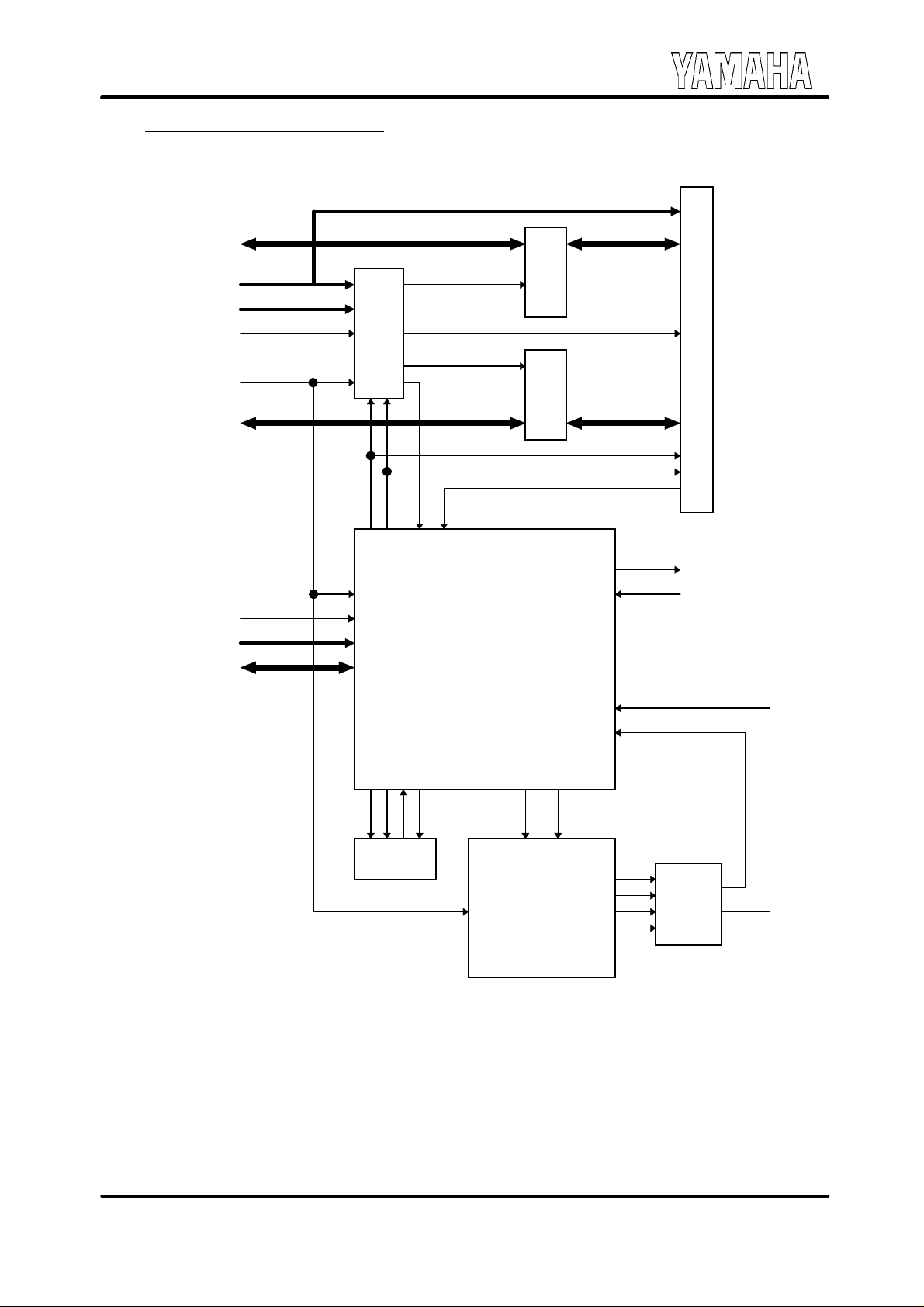
1-3. System Block Diagram
(1) SEL=1 (Sound Card and Combo Card Add-in)
SD15-8
SA2-0
SA15-12
AEN
RESETDRV
SD7-0
/IOW,/IOR
SA11-0
SD7-0
16V8
/CDCS1
/CDCS0
MP7
MP6
RESET
IOW,/IOR
A11-0
D7-0
ENH
RESET
ENL
CDIRQ
AEN*
MP8
AEN
YMF715E-S
(OPL3-SA3)
245
245
AUX2L
AUX2R
MP0
MP1
IDE CD-ROM I/F
MCS
MIRQ
MODEM I/F
}
MP3
MP2
MP4
ROMDI
ROMCS
ROMCL
EEPROM
MP5
ROMDO
TXD
MP9
TXD
CLKO
XI
RXD
CLKO
BCO
LRORESET
DO2
YAC516
OPL4-ML/ML2
1. External PAL(16V8 etc.)
(i) connect the signal AEN* generated by decoding SA15-12 and AEN to the AEN of OPL3-
SA3.
(ii) generate the /G(enable) signal for Data Bus Buffer (LS245) by decoding the /CDCS1-0 and
SA2-0.
(iii) generate the /RESET signal from RESETDRV.
May 21, 1997
-8-
Page 9
YMF715E
/
/
K
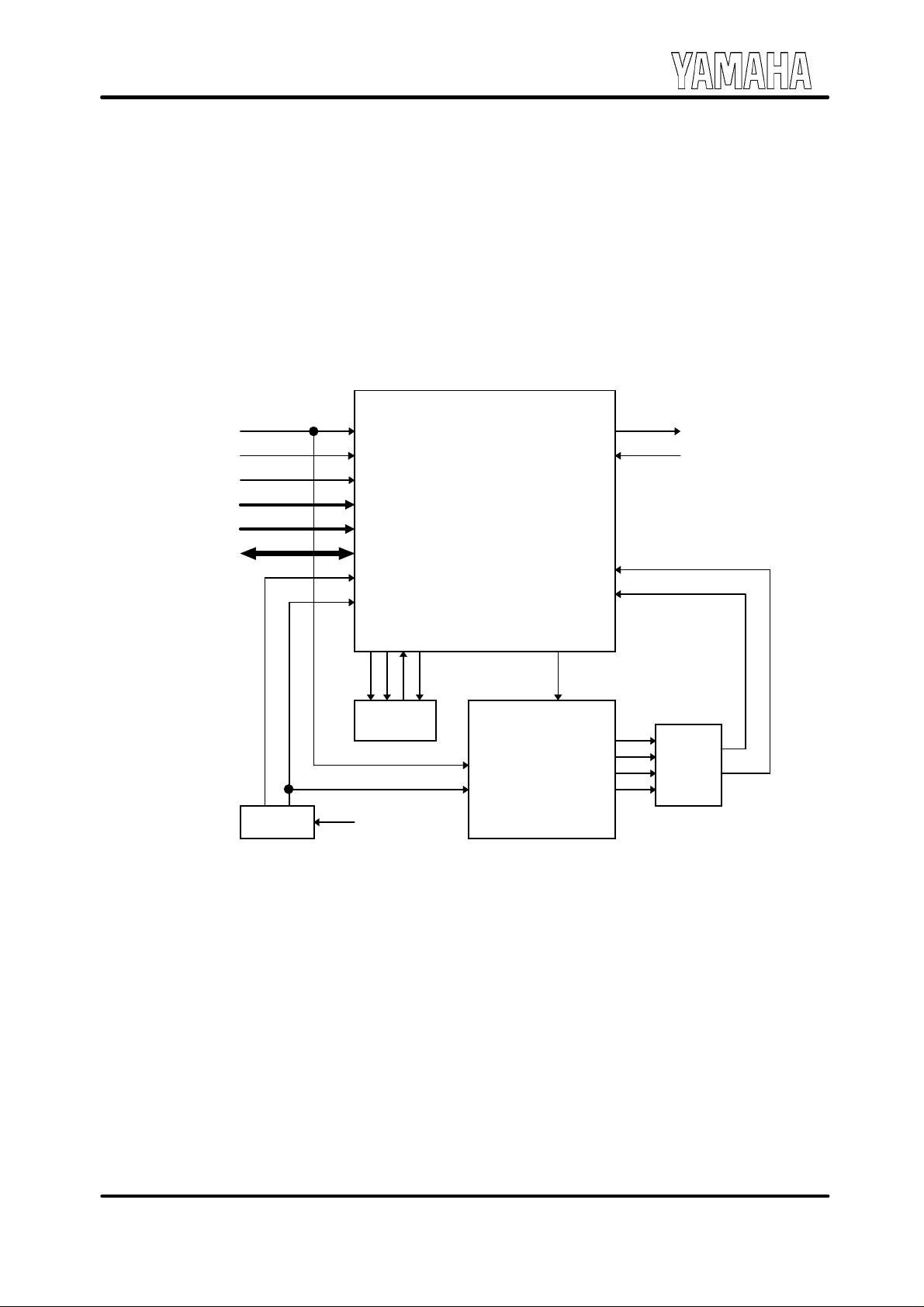
2. Master Clock
Both 33.8688MHz and 24.576MHz are used or 14.31818MHz and clock module
(ex.MK1420 by Micro Clock) are used.
3. OPL4-ML/ML2
The external DAC (YAC516) is necessary for wavetable upgrade.
(2) SEL=2 (Sound Card and Combo Card for Add-in)
RESETDRV
/IOW,/IOR
AEN
SA15-12
SA11-0
SD7-0
24.576MHz
33.8688MHz
MK1420
RESET
IOW,/IOR
AEN
MP9-6
A11-0
D7-0
X24I
X33I
MP2
ROMCL
YMF715E-S
(OPL3-SA3)
MP4
MP3
MP5
ROMDI
ROMCS
ROMDO
EEPROM
14.31818MHz
AUX2L
AUX2R
TXD
TXD
RXD
RESET
XI
OPL4-ML/ML2
MP0
MP1
CLKO
BCO
LRO
DO2
MCS
MIRQ
YAC516
MODEM I/F
}
1. OPL4-ML/ML2
The external DAC (YAC516) and the clock module (ex.MK1420 by Micro Clock) are
necessary for wavetable upgrade.
2. MK1420
The MK1420 is the clock module that generates all clocks necessary for this chipset . It is by
Micro Clock and its package is SOP8.
May 21, 1997
-9-
Page 10
YMF715E
/
K
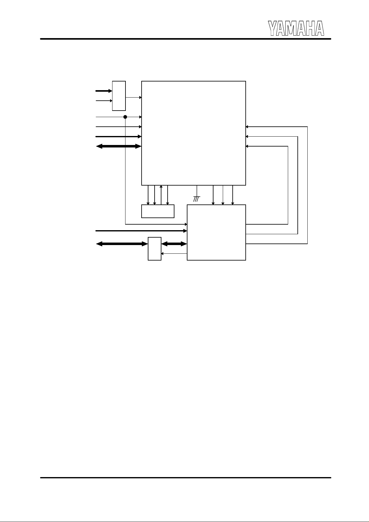
(3) SEL=3 (Sound Card for Add-in)
SA15-12
AEN
RESETDRV
/IOW,/IOR
SA11-0
SD7-0
/IOW,/IOR
SA2-0
SD7-0
AEN*
138
AEN
RESET
IOW,/IOR
A11-0
D7-0
MP3
MP2
MP4
ROMDI
ROMCS
ROMCL
EEPROM
245
YMF715E-S
(OPL3-SA3)
MP5
ROMDO
/EXTEN
RESET
/IOW
/IOR
A2-0
D7-0
DBDIR
MP0
OPL4-
ML/ML2
MP6
MP7
MP8
TXD
MP9
MP1
TXD
CLKO
/SYNCS
XII
/OPLCS
RXD
DO2
LRO
BCO
BCLK_ML
LRCK_ML
SIN_ML
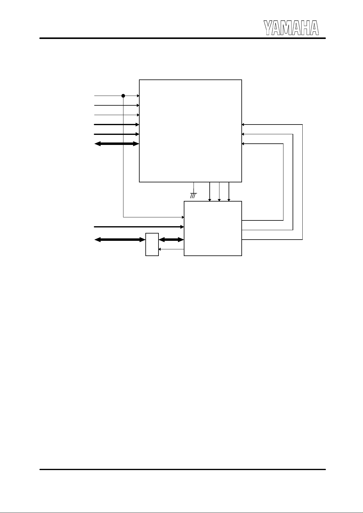
1. 16bit Address Decode
The signal AEN* generated by decoding SA15-12 and AEN needs to be connected to the
AEN of OPL3-SA3.
May 21, 1997
-10-
Page 11
YMF715E
/
/
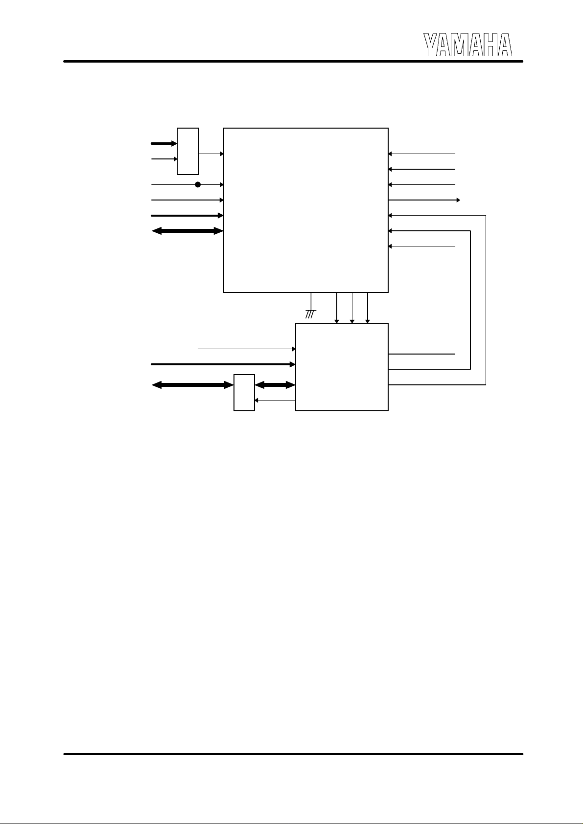
(4) SEL=4 (for Notebook PC)
SA15-12
AEN
RESETDRV
/IOW,/IOR
SA11-0
SD7-0
/IOW,/IOR
SA2-0
SD7-0
AEN*
138
AEN
RESET
IOW,/IOR
A11-0
D7-0
245
YMF715E-S
(OPL3-SA3)
MP0
MP1
/EXTEN
RESET
/IOW
/IOR
A2-0
D7-0
DBDIR
/SYNCS
/OPLCS
OPL4-
ML/ML2
MP2
MP3
MP4
MP5
MP6
MP7
MP8
TXD
MP9
TXD
CLKO
XII
RXD
DO2
LRO
BCO
BCLK_ZV
LRCK_ZV
SIN_ZV
XRST
BCLK_ML
LRCK_ML
SIN_ML
}
ZV Port
Peripheral
Equipment
1. 16bit Address Decode
The signal AEN* generated by decoding SA15-12 and AEN needs to be connected to the
AEN of OPL3-SA3.
2. ZV Port and OPL4-ML/ML2 I/F
ZV port is supported by using the internal DAC of OPL3-SA3 that is originally dedicated for
the use of internal OPL3.
(i) either OPL4-ML/ML2 or ZV port is active at a time and simultaneous use is not
possible.
(ii) which function the internal DAC is used for is determined by the SA3 Control
register, index 02h, VZE bit.
May 21, 1997
-11-
Page 12

YMF715E
/
/
/
(5) SEL=5 (for Notebook PC)
RESETDRV
/IOW,/IOR
AEN
SA15-12
SA11-0
SD7-0
24.576MHz
33.8688MHz
MK1420
RESET
IOW,/IOR
AEN
MP5-2
A11-0
D7-0
X24I
X33I
YMF715E-S
(OPL3-SA3)
14.31818MHz
MP0
MP1
MP6
MP7
MP8
MP9
AUX2L
AUX2R
TXD
TXD
RXD
RESET
XI
CLKO
OPL4-ML/ML2
BCO
LRO
DO2
BCLK_ZV
LRCK_ZV
SIN_ZV
XRST
YAC516
MCS
MIRQ
}
}
MODEM I/F
ZV Port
Peripheral
Equipment
1. Internal DAC
The internal OPL3 and the ZV Port shares the internal DAC, which is very similar to the case
mentioned the previous section.
(i) either internal OPL3 or ZV port is active at a time and simultaneous use is not
possible.
(ii) which function the internal DAC is used for is determined by the SA3 control
register, index 02h, VZE bit.
2. OPL4-ML/ML2
The external DAC (YAC516) and the clock module (ex.MK1420 by Micro Clock) are
necessary for wave table upgrade.
May 21, 1997
-12-
Page 13
YMF715E
/
(6) SEL=7 (for Notebook PC, Desktop P C )
RESETDRV
/IOW,/IOR
AEN
SA15-12
SA11-0
SD7-0
/IOW,/IOR
SA2-0
SD7-0
RESET
IOW,/IOR
AEN
MP5-2
A11-0
D7-0
245
YMF715E-S
(OPL3-SA3)
MP0
MP1
/EXTEN
RESET
/IOW
/IOR
A2-0
D7-0
DBDIR
/SYNCS
/OPLCS
OPL4-
ML/ML2
MP6
MP7
MP8
MP9
TXD
TXD
CLKO
XII
RXD
DO2
LRO
BCO
BCLK_ML
LRCK_ML
SIN_ML
May 21, 1997
-13-
Page 14

YMF715E
2. ISA Interface
OPL3-SA3 supports ISA Plug and Play (PnP) that frees the users from configuring the I/O address,
IRQ and DMA channel. Those system resources are set automatically by the system. However even
when used in Non PnP system, the configuration can be changed with software.
2-1. PnP Auto-Configuration mode
OPL3-SA3 has the following I/O port to support the Plug and Play ISA.
Address port: 279h
Write Data Port: A79h
Relocatable Read Data Port: 203h - 03FFh
The following four Logical Devices are supported by OPL3-SA3.
Logical Device No. 0
Sound Blaster compatible Playback system (SB Base)
16-bit CODEC (WSS Base)
MPU401 (MPU Base)
OPL3 (AdLib Base)
OPL3-SA3 control register (CTRL Base)
Logical Device No. 1
Joy Stick
Logical Device No. 2 (Optional)
MODEM (COM port)
Logical Device No. 3 (Optional)
IDE CD-ROM interface
-14-
May 21, 1997
Page 15
YMF715E
y
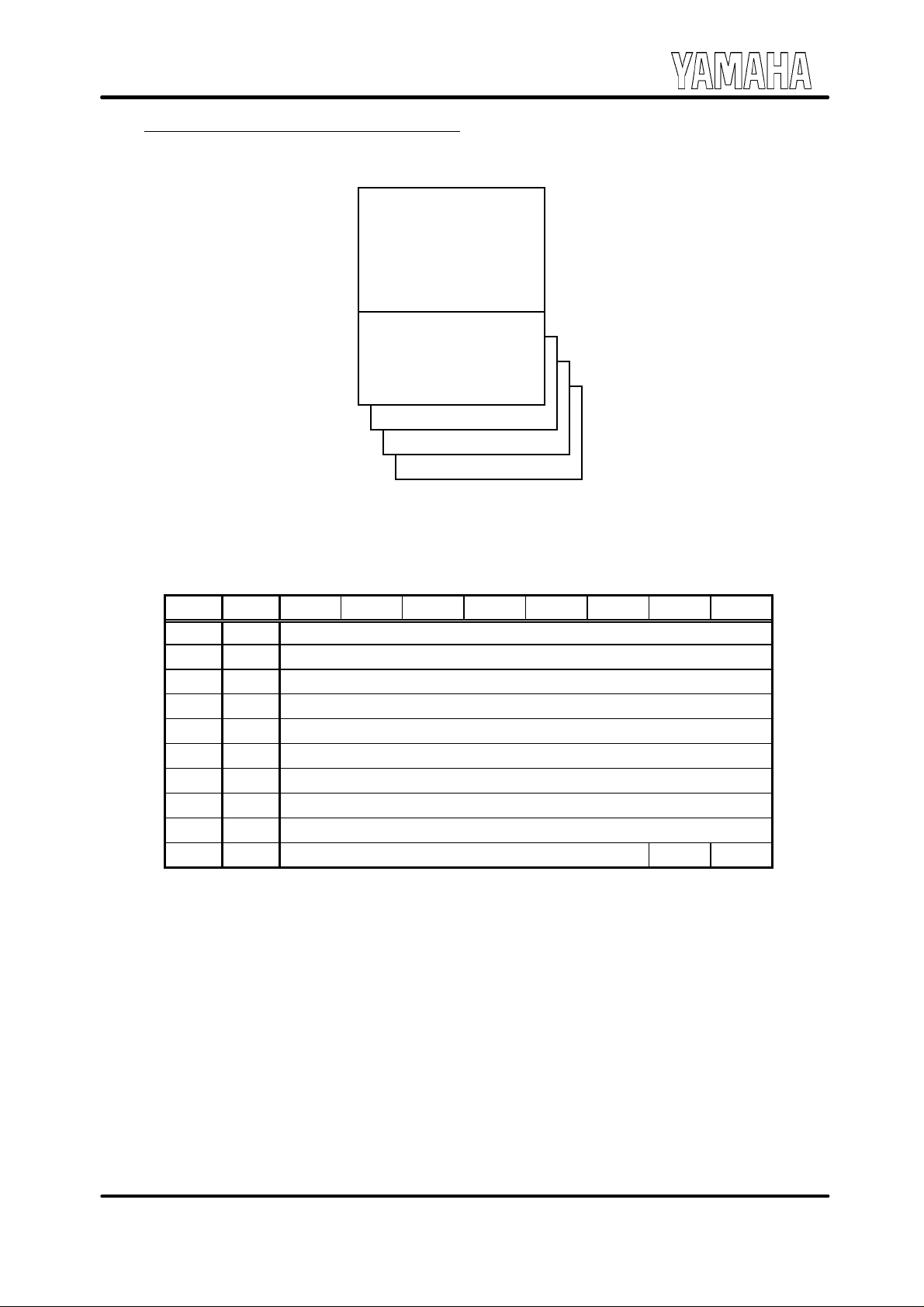
2-2. PnP ISA Configuration Register
OPL3-SA3 has the fo llowing Registers defined in the PnP ISA software.
0x00
0x22
0x30
Card Control
LDN=0, SA3 Sound S
0x75
LDN=1, Joy Stick
LDN=2, MODEM
LDN=3, CDROM
stem
Listed below is the register map of card control register and logical device registers. For the detailed
description of each register, please refer to the Plug and Play ISA Specification 1.0a
Card Control Registers
Index R/W D7 D6 D5 D4 D3 D2 D1 D0
00h W Set RD_DATA
01h R Serial Isolation
02h W Config Control
03h W Wake [CSN]
04h R Resource Data
05h R Status
06h R/W Card Select Number
07h R/W Logical Device Number
20h W Resource Data Write
21h W IKD RDWE
RDWE : Resource Data Write Enable
Setting “1” to this bit means the host can download the resources data to EEPROM and
internal SRAM via 20h.
IKD : Initiation Key Disable
Setting “1” to this bit means OPL3-SA3 should not detect the initiation key in the Wait for
Key state.
May 21, 1997
-15-
Page 16
YMF715E
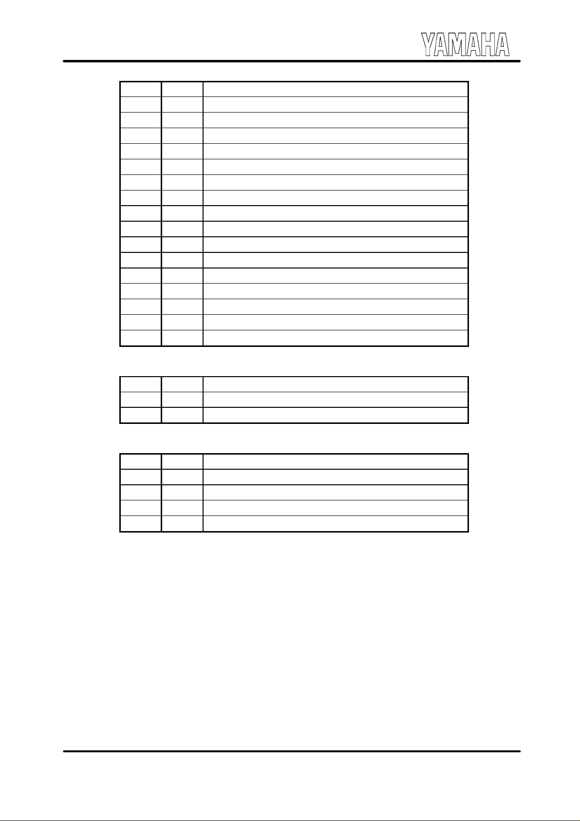
Logical Device Number = 0 : SA3 Sound System
30h R/W Activate
60h R/W I/O port base address[15..8], Descriptor 0 (SB base)
61h R/W I/O port base address[7..0], Descriptor 0 (SB base)
62h R/W I/O port base address[15..8], Descriptor 1 (WSS base)
63h R/W I/O port base address[7..0], Descriptor 1 (WSS base)
64h R/W I/O port base address[15..8], Descriptor 2 (AdLib base)
65h R/W I/O port base address[7..0], Descriptor 2 (AdLib base)
66h R/W I/O port base address[15..8], Descriptor 3 (MPU base)
67h R/W I/O port base address[7..0], Descriptor 3 (MPU base)
68h R/W I/O port base address[15..8], Descriptor 4 (CTRL base)
69h R/W I/O port base address[7..0], Descriptor 4 (CTRL base)
70h R/W Interrupt request level select 0 (for IRQ-A)
71h R Interrupt request type select 0 (for IRQ-A)
72h R/W Interrupt request level select 1 (for IRQ-B)
73h R Interrupt request type select 1 (for IRQ-B)
74h R/W DMA channel select 0 (for DMA-A)
75h R/W DMA channel select 1 (for DMA-B)
Logical Device Number = 1 : Joystick
30h R/W Activate
60h R/W I/O port base address[15..8]
61h R/W I/O port base address[7..0]
Logical Device Number = 2 : MODEM (Optional)
30h R/W Activate
60h R/W I/O port base address[15..8]
61h R/W I/O port base address[7..0]
70h R/W Interrupt request level select
71h R Interrupt request type select
-16-
May 21, 1997
Page 17
YMF715E
Logical Device Number = 3 : CD-ROM (Optional)
30h R/W Activate
60h R/W I/O port base address [15..8], Descriptor 0 (/CDCS0)
61h R/W I/O port base address [7..0], Descriptor 0 (/CDCS0)
62h R/W I/O port base address [15..8], Descriptor 1 (/CDCS1)
63h R/W I/O port base address [7..0], Descriptor 1 (/CDCS1)
70h R/W Interrupt request level select
71h R Interrupt request type select
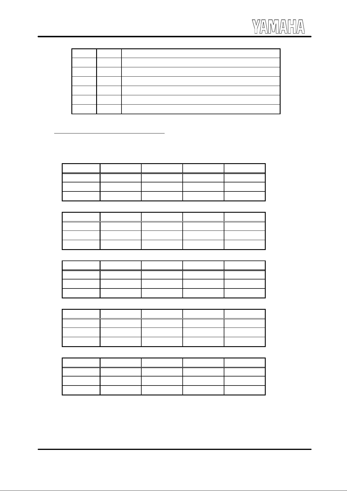
2-3. Recommended Resource Data
The recommended resource data is the followings.
(1) LDN=0:SA3 Sound System
I/O (SB base): 16bit address decode
Index Best Acceptable1 Acceptable2 Acceptable3
I/O 220h 240h 220-280h <-
Length 16 16 16 <-
Alignment - - 16 <-
I/O (WSS base): 16bit address decode
Index Best Acceptable1 Acceptable2 Acceptable3
I/O 530h E80h 530-F48h <-
Length 8 8 8 <-
Alignment - - 8 <-
I/O (AdLib base): 16bit address decode
Index Best Acceptable1 Acceptable2 Acceptable3
I/O 388h <- 388-3F8h <-
Length 8 <- 8 <-
Alignment - - 8 <-
I/O (MPU base): 16bit address decode
Index Best Acceptable1 Acceptable2 Acceptable3
I/O 330h 300h 300-334h <-
Length 2 2 2 <-
Alignment - - 2 <-
I/O (CTRL base): 16bit address decode
Index Best Acceptable1 Acceptable2 Acceptable3
I/O 370h 100-FFEh <- <-
Length 2 2 <- <-
Alignment - 2 <- <-
-17-
May 21, 1997
Page 18

YMF715E
IRQ-A: high-active, edge-sense
Index Best Acceptable1 Acceptable2 Acceptable3
IRQ 10 7,9,10,11 5,7,9,10,11 <-
IRQ-B: high-active, edge-sense
Index Best Acceptable1 Acceptable2 Acceptable3
IRQ 5 5,7 5 ,7,9,10,11 <-
DMA-A: 8bit, count by byte, type-A, B, F
Index Best Acceptable1 Acceptable2 Acceptable3
DMA 0 0,1,3 0,1,3 <-
DMA-B: 8bit, count by byte, type-A, B, F
Index Best Acceptable1 Acceptable2 Acceptable3
DMA 1 0,1,3 0,1,3 <-
(2) LDN=1:Joystick
I/O (Game Port): 16bit address decode
Index Best Acceptable1 Acceptable2 Acceptable3
I/O 201h 202h 203h 204-20Fh
Length 1 1 1 1
Alignment - - - 1
(3) LDN=2:MODEM
I/O (/MCS): 16bit address decode
Index Best Acceptable1 Acceptable2 Acceptable3
I/O 2F8h 100-FF8h <- <-
Length 8 8 <- <-
Alignment - 8 - -
IRQ: high-active, edge-sense
Index Best Acceptable1 Acceptable2 Acceptable3
IRQ 3 <- <- <-
-18-
May 21, 1997
Page 19

YMF715E
(4) LDN=3:CD-ROM
I/O (/CDCS0): 16bit address decode
Index Best Acceptable1 Acceptable2 Acceptable3
I/O 1E8h 100-1F8h <- <-
Length 8 8 <- <-
Alignment - 8 <- <-
I/O (/CDCS1): 16bit address decode
Index Best Acceptable1 Acceptable2 Acceptable3
I/O 3EEh 306-3F6h <- <-
Length 1 1 <- <-
Alignment - 8 <- <-
IRQ: high-active, edge-sense
Index Best Acceptable1 Acceptable2 Acceptable3
IRQ 11 3,5,7,9,10,11 <- <-
2-4. Manual Configuration Mode
When OPL3-SA3 is in the Wait for Key state, it can be changed to the Manual Configuration mode
by sending the following YAMAHA key to Address_Port. The Manual Configuration mode is used
for downloading the resource data to EEPROM and internal SRAM, setting up the OPL3-SA3
without PnP protocol.
YAMAHA Key:
B1h, D8h, 6Ch, 36h, 9B h, 4Dh, A6h, D3h,
69h, B4h, 5Ah, ADh, D6h, EBh, 75h, BAh,
DDh, EEh, F7h, 7Bh, 3Dh, 9Eh, CFh, 67h,
33h, 19h, 8Ch, 46h, A3h, 51h, A8h, 54h
In the Manual Configuration mode, PnP registers can be accessed by the host without PnP protocol.
Right after OPL3-SA3 is switched to the Manual Configuration mode, set “81h” in CSN register
automatically to put OPL3-SA3 in ‘Sleep’ State. And when “81h” is written to Wake [CSN], it
becomes possible to access to Configuration register of each logical device from the host.
To return from the Manual Configuration mode to PnP auto-configuration mode, the Wait for Key
command should be sent.
Note :
The Manual Configuration mode can not be used in the system with more than one OPL3-SA3’s card
installed in the ISA slot.
-19-
May 21, 1997
Page 20

YMF715E
3. Download Resource data
When OPL3-SA3 is in the Configuration state, the host can download the resources data to EEPROM
and internal SRAM via 20h: Resource Data Write. To switch OPL3-SA3 into configuration mode,
there are two methods.
First method is to use the normal PnP protocol. After CSN was assigned for all ISA cards by PnP software, get CSN from CM (configuration manager) and write the CSN to Wake [CSN], then OPL3-SA3
switches into configuration state.
Second method is to use the YAMAHA Key sequence which is described in the Manual Configuration
mode section. After OPL3-SA3 detects YAMAHA key, OPL3-SA3 switches into the Sleep state.
Writing “81h” to Wake [CSN] re gister changes OPL3-SA3 into Co nfiguration state.
After OPL3-SA3 switches into the Configuration state, download the Resource data to EEPROM and
internal SRAM by using following sequence.
1. Write “01h”(RDWE bit = “1”) to 21h: Resource Data Write Enable register to reset
internal address counter and to enable downloading the data.
2. Write Resource data to 20h: Resource Data Write register until downloading data is
completed.
3. Write “00h” to 21h: Resource Data Write Enable register to disable downloading .
4. External EEPROM
The resource data information of OPL3-SA3 used for PnP auto configuration is stored in external
EEPROM. And either 256 x 16-bit EEPROM or 128 x 16-bit EEPROM, such as 93C55, 93C56,
93C65, 93C66 should be used.
5. Hardware Volume Control
5-1. Hardware Volume up/down/mute Control
Two digital input pins; /VOLUP and /VOLDW can control the master volume of OPL3-SA3.
When /VOLUP is low level, register value of master volume is decremented(-1). When the value
reaches to “00h”(max.0dB), the input signal will not be effective.
When /VOLDW is low level, register value of master volume is incremented(+1). When the value
reaches to “0Fh”(min.-30dB), the input signal will not be effective.
When both of the /VOLUP and /VOLDW are low level simultaneously, volume is muted. When either
/VOLUP or /VOLDW is low level, the previous value becomes effective, and volume is no mute.
5-2. Hardware Volume Interrupt
If configured VEN( Hardware Vo lume Enable)= 1, SA3 Control Registe r, index 0Ah, D7 b it, when one
of the hardware volume control pins /VOLUP or /VOLDW is asserted or when both are asserted to
request mute, interrupt will be posted in the interrupt channel specified in SA3 Control Register, index
17h, IRQ-A MV or IRQ-B MV bit.
Note that when the muting is in effect, the subsequent mute requests which does not change any
register contents will generate interrrupts. The ignored UP/DOWN requests (UP requests with 0dB
Volume attn., DOWN requests with -30dB) will not generate interrupts.
This bit is cleared upon host’s reading the Master Volume Lch register, SA3 Control Register, index
07h.
-20-
May 21, 1997
Page 21

YMF715E
g
6. DAC interface
OPL3-SA3 supports two types of DAC interface format. One is the conventional DAC interface format
(very common for the consumer audio product) for OPL4-ML/ML2. Another is the I
Zoomed Video port. These two types of the formats are shown in the following Fig.6-1, 2.
BCLK
2
S format for
SIN
LRCK
BCLK
SIN
LRCK
010123456789101115 14 13 12 0123456789101115 14 13 12
Left Channel Right Channel
Fig.6-1 Conventional DAC Interface Format for OPL4-ML/ML2
14 13 12 0123456789101115 14 13 12
Fig.6-2 I2S F ormat for Zoomed Video Port
0123456789101115
Ri
ht ChannelLeft Channel
7. 3D Enhanced Control
OPL3-SA3 integrates the 3D enhanced controller including all the analog components in conventional
systems. Wide, bass, and treble controls are available via SA3 control register, index 14h, 15h, 16h.
One of the four 3D Enhancement modes can be selected according to the frequency response of the
speaker. These are controlled by SA3 control register, index 02h D5, D4 bit (YMODE1-0).
YMODE1 YMODE0 3D Enhancement mode Target speaker Speaker size
0 0 Desktop mode Standard speaker 5 ~ 12cm
0 1 Notebook PC mode (1) Small speaker 3cm
1 0 Notebook PC mode (2) Smaller speaker 1.5cm
1 1 Hi-Fi mode Hi-Fi speaker 16 ~ 38cm
Following diagram(Fig.7-1) shows the 3D enhanced controller sub-system.
MIC,LINER,
AUX1R,AUX2R,
{
MIN,SBR,WSS_PBR
Yamaha
Rch
3D Enhanced
}
{
MIC,LINEL,
AUX1L,AUX2L,
MIN,SBL,WSS_PBL
Controller
(analog components)
Fig.7-1 3D Enhanced Control Block Diagram
-21-
Lch
to Hardware
Volume Control
May 21, 1997
Page 22

YMF715E
8. Power Management
Following 4 functionalities are provided for APM(Advanced Power Management) compliance.
(1) Partial Power Down Mode
(2) Power Save Mode
(3) Global Power Down Mode
(4) Suspend/Resume Mode
Plug and Play
Clock
Generator
Recording
WSS-
WSS-Playback
FM(OPL3)
Sound Blaster
Clock-
out
1bit D/A
SCF
1bit A/D
SCF
FM
DAC
SB
DAC
MPU
401
(Wide Stereo)
3D Enahaced Controller
Joy-
Stick
VREF
Mixing Circuit
Global Power Down
:
Power Save 1,2
:
Partial Power Down (digital) : 8 digital blocks can be disabled independently.
:
Partial Power Down (analog) : 5 analog blocks can be disabled independently.
:
Fig.8-1 Power Management
-22-
May 21, 1997
Page 23

YMF715E
8-1. Partial Power Down Mode
Functional blocks comprising OP L3-SA3 which are shown in Fig.8-1, are designed so they can be
disabled independent of each other. SA3 control register, index 12h and 13h, implements these
controls (see section 9-1-5).
,
the OPL3-SA3 dissipates more power with all these blocks “partial power down”ed than that can be
achieved in “power save mode 2”.
In this mode, master volume is not muted, so all analog input sources and enabled digital sources (i.e.
FM, SB, WSS etc.) can be heard.
Note :
AUX2 inputs are exceptions in this regard since setting FM-DAC at index 13h of SA3 Control
Register inhibits the inputs altogether.
8-2. Power Save Mode
SA3 control register, index 01h, PSV and PDX bits, implement these controls.
Clock generator can be controlled under either two options.
(i) Power Save Mode 1 (Clock Generator Control : Disabled (stop)) (PSV=PDX=1)
It is necessary to take some time before clock oscillation to stabilize. Power dissipation of digital
portion becomes about 100uA(typ.), and that of analog portion becomes about 5mA(typ.).
(ii) Power Save Mode 2 (Clock Generator Control : Enabled (crystals keep on oscillating))
(PSV=1, PDX=0)
Leaving power save mode gets the OPL3-SA3 back into function instantly. Power dissipation of
digital portion becomes about 10mA(typ.), and that of analog portion becomes about 5mA(typ.).
In these power save modes, the OUTL/R pins will keep the VREF voltage. During these modes,
master volume is automatically muted, so all audio sources can not heard. After resuming from these
modes, master volume is still muted.
blocks in the above diagram show those that can be disabled/enabled. Note, however,
8-3. Global Power Down Mode
This mode is to minimize power dissipation by stopping all the function of OPL3-SA3. It is
necessary to take some time before clock oscillation to stabilize. To tal dissipation becomes about
10uA(typ.).
VREF voltage slowly decays to ground on transition into this mode, and quickly returns to VREF on
transition from this mode. During this mode, master volume is automatically muted, so all audio
sources can not heard. After resuming from this mode, master volume is still muted.
(PDN=PDX=1)
-23-
May 21, 1997
Page 24

YMF715E
8-4. Suspend/Resume Mode
There is no “read only” or “hidden state” registers in OPL3-SA3. This means you can always read
and save these values before power off and can set those values back in registers after reset or power
on to achieve the suspend/resume capability.
Correspondence to APM
APM OPL3-SA3 WIN(Driver) BIOS
ON ON
APM Enabled Partial Power Down
APM Standby Power Save(Down)
APM Suspend OFF
OFF OFF
Note : Analog Power OFF Feature
OPL3-SA3 has the special feature that the Analog power supplies can be removed from OPL3-SA3. This
feature is independent of digital portion.
○○
○×
○○
○○
○○
-24-
May 21, 1997
Page 25

YMF715E
9. Register description
9-1. SA Sound System
9-1-1. OPL3
Listed below are the OPL3-L register for AdLib compatibility.
AdLib base (R) Status Register port
AdLib base (W) Address port for Register Array 0
AdLib base + 1 (R/W) Data port
AdLib base + 2 (W) Address port for Register Array 1
AdLib base + 3 (R/W) Data port
Wavetable upgrade (OPL4-ML/ML2) is available by setting /EXTEN (SEL=3, 4, 7) to “L”. And,
additional I/O ports listed below can also be accessed. In case of SB mode, AdLib base + 2, 3 is write
only registers.
AdLib base + 4 (R) Status port for Wavetable Register
AdLib base + 4 (W) Address port for Wavetable Register
AdLib base + 5 (R/W) Data port Wavetable Register
AdLib base + 6 (R/W) Command port for MIDI processor
AdLib base + 7 (R) Status port for MIDI processor
AdLib base + 7 (W) Control port for MIDI processor
OPL3 Status Register (RO):
Index D7 D6 D5 D4 D3 D2 D1 D0
xxh IRQ FT1 FT2 - - BUSY - BUSY
OPL3 Data Register Array 0 (R/W):
Index D7 D6 D5 D4 D3 D2 D1 D0
00 - 01h LSI TEST
02h TIMER 1
03h TIMER 2
04h RST MT1 MT2 - - - ST2 ST1
08h-NTS-----20 - 35h AM VIB EGT KSR MULT
40 - 55h KSL TL
60 - 75h AR DR
80 - 95h SL RR
A0 - A8h F-NUM (L)
B0 - B8h - - KON BLOCK F-NUM (H)
BDh DAM DVB RHY BD SD TOM TC HH
C0 - C8h * * CHR CHL FB CNT
E0 - F5h - - - - - WS
-25-
May 21, 1997
Page 26

YMF715E
OPL3 Data Register Array 1 (R/W)
Index D7 D6 D5 D4 D3 D2 D1 D0
00 - 01h LSI TEST
04h - - CONNECTION SEL
05h - - - - - NEW3 * NEW
20 - 35h AM VIB EGT KSR MULT
40 - 55h KSL TL
60 - 75h AR DR
80 - 95h SL RR
A0 - A8h F-NUM (L)
B0 - B8h - - KON BLOCK F-NUM (H)
C0 - C8h * * CHR CHL FB CNT
E0 - F5h - - - - - WS
The bit remarked * indicates that these can be read and written but not effective.
Note :
The wait time of 960ns(min.) is needed before access to OPL3 registers.
9-1-2. Sound Blaster Pro compatibility
The followings are the I/Os for Sound Blaster Pro compatibility.
SB base (R) OPL3 Status port
SB base (W) OPL3 Address port for Register Array 0
SB base + 1h (R/W) OPL3 Data register
SB base + 2h (W) OPL3 Address port for Register Array 1
SB base + 3h (R/W) OPL3 Data port
SB base + 4h (W) SB Mixer Address port
SB base + 5h (R/W) SB Mixer Data port
SB base + 6h (W) DSP Reset port
SB base + 8h (R) OPL3 Status port
SB base + 8h (W) OPL3 Address port for Register Array 0
SB base + 9h (R/W) OPL3 Data port
SB base + Ah (R) DSP Read Data port
SB base + Ch (R) DSP Write-buffer status port
SB base + Ch (W) DSP Write Command/Data port
SB base + Eh (R) DSP Read-buffer status port
-26-
May 21, 1997
Page 27

YMF715E
9-1-2-1. DSP Command
Listed below are the supported commands of DSP defined Sound Blaster Pro compatibility.
CMD Support Function
10h o 8bit direct mode digitized sound I/O output
14h o 8bit single-cycle DMA mode digitized sound output
16h *1 8bit to 2bit ADPCM single-cycle DMA mode digitized sound output
17h *1 8bit to 2bit ADPCM single-cycle DMA mode digitized sound output with ref. byte
1Ch o 8bit auto-init DMA mode digitized sound output
1Fh *1 8bit to 2bit ADPCM auto-init DMA mode digitized sound output with ref. byte
20h *1 8bit direct mode single byte digitized sound input
24h *1 8bit single-cycle DMA mode digitized sound input
2Ch *1 8bit auto-init DMA mode digitized sound input
30h o Polling mode MIDI input
31h o Interrupt mode MIDI input
34h o UART polling mode MIDI I/O
35h o UART interrupt mode MIDI I/O
36h o(*2) UART polling mode MIDI I/O with time stamping
37h o(*2) UART interrupt mode MIDI I/O with time stamping
38h o MIDI output
40h o Set digitized sound transfer Time Constant
48h o Set DSP block transfer size
74h o 8bit to 4bit ADPCM single-cycle DMA mode digitized sound output
75h o 8bit to 4bit ADPCM single-cycle DMA mode digitized sound output with ref. byte
76h *1 8bit to 3bit ADPCM single-cycle DAM mode digitized sound output
77h *1 8bit to 3bit ADPCM single-cycle DMA mode digitized sound output with ref. byte
7Dh o 8bit to 4bit ADPCM auto-init DMA mode digitized sound output with ref. byte
7Fh *1 8bit to 3bit ADPCM auto-init DMA mode digitized sound output with ref. byte
80h o Pause DAC for a duration
90h o 8bit high-speed auto-init DMA mode digitized sound output
91h o 8bit high-speed single-cycle DMA mode digitized sound output
98h *1 8bit high-speed auto-init DMA mode digitized sound input
99h *1 8bit high-speed single-cycle DMA mode digitized sound input
A0h *1 Set input mode to mono
A8h *1 Set input mode to stereo
D0h o Pause 8bit DMA mode digitized sound I/O
D1h *1 Turn on speaker
D3h *1 Turn off speaker
D4h o Continue 8bit DMA mode digitized sound I/O
D8h *1 Get speaker status
DAh o Exit 8bit auto-init DMA mode digitized sound I/O
E1h o Get DSP version number
Note :
*1) These commands are performed in state-machine, but they are not effective.
*2) MIDI data can not be received.
Additional undocumented commands are included.
-27-
May 21, 1997
Page 28

YMF715E
)
9-1-2-2. Sound Blaster Pro compatibility Mixer
The table below is the register map of mixer of Sound Blaster Pro compatibility.
Index D7 D6 D5 D4 D3 D2 D1 D0
00h Reset Mixer
04h Voice Vol. Lch - Voice Vol. Rch
0Ah----- MIC Vol. -
Input
0Ch - -
0Eh - -
22h Master Vol. Lch - Master Vol. R -
26h MIDI Vol. Lch - MIDI Vol. Rch -
28h CD Vol. Lch - CD Vol. Rch -
2Eh Line Vol. Lch - Line Vol. Rch -
Filter
Output
Filter
Low Pass
-
---
Filter
Input Source -
Stereo
SW
-
The bit remarked indicates that these can be read and written but not effective.
The actual value written to the Master Vol., MIDI Vol., CD Vol. and Line Vol. is based on the table
shown below. And when read, actual value cannot be read and written value to each register is read
instead.
Voice Vol. (04h), CD Vol. (28h), Line Vol. (2Eh
01234567
0
mute mute mute mute mute mute mute mute
1
mute -28.5dB -22.5dB -16.5dB -10.5dB -7.5dB -3.0dB 0dB
2
mute -22.5dB -16.5dB -10.5dB -7.5dB -3.0dB 0dB 0dB
3
mute -16.5dB -10.5dB -7.5dB -3.0dB 0dB 0dB 0dB
4
mute -10.5dB -7.5dB -3.0dB 0dB 0dB 0dB 0dB
5
mute -7.5dB -3.0dB 0dB 0dB 0dB 0dB 0dB
6
mute -3.0dB 0dB 0dB 0dB 0dB 0dB 0dB
7
mute 0dB 0dB 0dB 0dB 0dB 0dB 0dB
May 21, 1997
-28-
Page 29

YMF715E
)
0
1
2
3
4
5
6
7
Mixer register
SB Mixer WSS Mixer
MIDI Vol.
CD Vol.
Line Vol.
MIDI Vol. (26h
0123456 7
mute mute mute mute mute mute mute mute
mute -24.0dB -18.0dB -12.0dB -6.0dB -3.0dB +1.5dB +4.5dB
mute -18.0dB -12.0dB -6.0dB -3.0dB +1.5dB +4.5dB +4.5dB
mute -12.0dB -6.0dB -3.0dB +1.5dB +4.5dB +4.5dB +4.5dB
mute -6.0dB -3.0dB +1.5dB +4.5dB +4.5dB +4.5dB +4.5dB
mute -3.0dB +1.5dB +4.5dB +4.5dB +4.5dB +4.5dB +4.5dB
mute +1.5dB +4.5dB +4.5dB +4.5dB +4.5dB +4.5dB +4.5dB
mute +4.5dB +4.5dB +4.5dB +4.5dB +4.5dB +4.5dB +4.5dB
→
→
→
AUX2 Vol.
AUX1 Vol.
Line Vol.
default
SB Mixer
Master Vol. = (99h)
MIDI Vol. = +4.5dB (99h)
Voice Vol. = 0dB (99h)
CD Vol. = mute (11h)
Line Vol. = mute (11h)
WSS Mixer
AUX2 Vol. = +4.5dB (05h)
AUX1 Vol. = mute (88h)
Voice Vol. = mute (80h)
Line Vol. = mute (88h)
Mono Vol. = mute(MIN, MOUT) (C0h)
SA3 CTRL
Master Vol. = -14dB (07h)
MIC Vol. = mute (88h)
May 21, 1997
-29-
Page 30

YMF715E
9-1-3. WSS compatible 16-bit CODEC
The followings are the I/Os for Window Sound System compatibility.
WSS base (R) WSS Co nfiguration Register port
WSS base + 3h (R) WSS Status Register port
WSS base + 4h (R/W) WSS CODEC Index address port
WSS base + 5h (R/W) WSS CODEC Index data port
WSS base + 6h (R/W) WSS CODEC Status port
WSS base + 7h (R/W) WSS CODEC PIO Data port
WSS Configuration Register (RO):
portD7D6D5D4D3D2D1D0
+0h “0” “0” IRQ DMA
This register is used to indicate what resources is assigned and it is read only register.
IRQ:
DMA:
Notice)
In the case that CODEC is in Dual DMA mode, only playback DMA channels are valid
and recording DMA channels are ignored.
“0”: No interrupt channel is available
“1”: IRQ7 is available
“2”: IRQ9 is available
“3”: IRQ10 is available
“4”: IRQ11 is available
“5”-”7”: reserved.
“0”: No DMA channel is available
“1”: DMA0
“2”: DMA1
“3”: DMA3
“4”-“7”: reserved
WSS Status Register (RO):
portD7D6D5D4D3D2D1D0
+03h SBHC “0” “04h”
WSS CODEC Direct Registers (R/W):
portD7D6D5D4D3D2D1D0
+4h INIT MCE TRD Index Address
+5h Index Data
+6h CU/L CL/R CRDY SER PU/L P/R PRDY INT
+7h PIO Data
May 21, 1997
-30-
Page 31

YMF715E
WSS CODEC Indirect Registers (R/W):
Index D7 D6 D5 D4 D3 D2 D1 D0
00h LSS1 LSS0 LMGE - LIG3 LIG2 LIG1 LIG0
01h RSS1 RSS0 RMGE - RIG3 RIG2 RIG1 RIG0
02h LX1M - - LX1G4 LX1G3 LX1G2 LX1G1 LX1G0
03h RX1M - - RX1G4 RX1G3 RX1G2 RX1G1 RX1G0
04h LX2M - - LX2G4 LX2G3 LX2G2 LX2G1 LX2G0
05h RX2M - - RX2G4 RX2G3 RX2G2 RX2G1 RX2G0
06h LOM - LOA5 LOA4 LOA3 LOA2 LOA1 LOA0
07h ROM - ROA5 ROA4 ROA3 ROA2 ROA1 ROA0
08h FM1 FM0 C/L S/M CFS2 CFS1 CFS0 CSL
09h CPIO PPIO - - ACAL SDC CEN PEN
0Ah XTL1* XTL0* - - - - IEN -
0Bh COR PUR ACI DRS “0” “0” “0” “0”
0Ch MID MODE - - ID3 ID2 ID1 ID0
0Dh LBA5 LBA4 LBA3 LBA2 LBA1 LBA0 - LBE
0Eh PUB7 PUB6 PUB5 PUB4 PUB3 PUB2 PUB1 PUB0
0Fh PLB7 PLB6 PLB5 PLB4 PLB3 PLB2 PLB1 PLB0
10h OLB TE CMCE PMCE - - - DACZ
11h-------HPF*
12h LLM - - LLG4 LLG3 LLG2 LLG1 LLG0
13h RLM - - RLG4 RLG3 RLG2 RLG1 RLG0
14h TL7 TL6 TL5 TL4 TL3 TL2 TL1 TL0
15h TU7 TU6 TU5 TU4 TU3 TU2 TU1 TU0
16h--------
17h--------
18h - TI CI PI CU CO PO PU
19h V2 V1 V0 - - CID2 CID1 CID0
1Ah MIM - - - MIA3 MIA2 MIA1 MIA0
1Bh--------
1Ch FMT1 FMT0 C/L S/M - - - 1Dh--------
1Eh CUB7 CUB6 CUB5 CUB4 CUB3 CUB2 CUB1 CUB0
1Fh CLB7 CLB6 CLB5 CLB4 CLB3 CLB2 CLB1 CLB0
The bit remarked * indicates that these can be read and written but not effective.
-31-
May 21, 1997
Page 32

YMF715E
Mixer default:
02h:AUX1L = 88h (mute)
03h:AUX1R = 88h (mute)
04h:AUX2L = 05h (+4.5dB)
05h:AUX2R = 05h (+4.5dB)
06h:DACL = 80h (mute)
07h:DACR = 80h (mute)
12h:LineL = 88h (mute)
13h:LineR = 88h (mute)
1Ah:MonoIn = C0h ( mute)
9-1-4. MPU401
The followings are the I/Os for MPU401 compatibility.
MPU base (R/W) MIDI Data port
MPU base +1 (R) Status Register port
MPU base + 1 (W) Command Register port
9-1-5. OPL3-SA3 control register
This register is used to control the additional functions (ex. power management, wide stereo).
CTRL base (R/W) Index port
CTRL base +1 (R/W) Data port
Power Management (R/W):
Index D7 D6 D5 D4 D3 D2 D1 D0
01h “0” “0” ADOWN “0” “0” PSV PDN PDX
ADOWN (Analog Down)... Analog power supplies can be removed from OPL3-SA3, if
ADOWN=“1”.
Set this bit to “0”, before analog power is supplied again.
PSV (power save)... Setting this bit to “1” makes OPL3-SA3 in power save mode
that is categorized into two types.
Power save mode 1
where PSV=PDX=”1”, clock oscillation is disabled and power
dissipation of digital portion becomes about 100uA(typ.), and that of
analog portion becomes about 5mA(typ.).
Power save mode 2
where PSV=”1” and PDX=0, clock oscillation is active. However
power dissipation of digital portion becomes about 10mA(typ.), and
that of analog portion becomes about 5mA(typ.).
PDN (Power down)... Setting this bit to “1” makes in power down mode.
PDX (Oscillation stop)... Setting this bit to “1” makes the clock oscillation halt.
default : 00h
-32-
May 21, 1997
Page 33

YMF715E
Notice)
1) Set D7, D6, D4 and D3 bits to “0”.
2) In the power save modes 1, 2, the OUTL/R pins will keep the VREF voltage. In the power down
mode, VREF voltage slowly decays to ground on transition into this mo de, and quickly returns to
VREF on transition from this mode. During these modes (power save/down), master volume is
automatically muted, so all audio sources cannot be heard. After resuming these modes, master
volume is still muted.
3) The Joystick portion must be re-initialized by writing any value to the Jo ystick por t after resuming
from the power down/save mode.
System control (R/W):
Index D7 D6 D5 D4 D3 D2 D1 D0
02h SBHE - YMODE1 YMODE0 - IDSEL1 IDSEL0 VZE
SBHE... When AT-bus is used, set to “0” and set to “1” in case of XT-bus.
YMODE1-0... 3D Enhancement mode according to the application can be selected
IDSEL1, IDSEL0... These two bits specify the DSP version of Sound B laster compatible
by these two bits as follows.
YMODE1 YMODE0 3D Enhancement mode
0 0 Desktop mode
0 1 Notebook PC mode (1)
1 0 Notebook PC mode (2)
1 1 Hi-Fi mode
portion.
The different return value of DSP command E1h (Get DSP version
number) of Sound Blaster Pro is got by these bits in.
1st byte 2nd byte
IDSEL1 IDSEL0 (major ver) (minor ver)
0 0 03h 01h
0 1 02h 01h
1 0 01h 05h
1 1 00h 00h
VZE... I2S audio format can be fed to BCLK_ZV, LRCK_ZV, SIN_ZV pins
of OPL3-SA3 by setting this bit to “1” regardless of the /EXTEN,
when Zoomed Video port is in use.
default : 00h
Notice)
Input signals, BCLK_ZV and LRCK_ZV pins which appear on SEL=4 or 5 mode, should be
oscillated, when VZE=1.
May 21, 1997
-33-
Page 34

YMF715E
Interrupt Channel configuration (R/W):
Index D7 D6 D5 D4 D3 D2 D1 D0
There are four devices (WSS (Windows Sound System CODEC), SB (Sound Blaster
compatible portion), OPL3, MPU (MPU401)) that can be an interrupt source. This
register specifies what interrupt source is routed to two physical interrupt (IRQA and
IRQB) of OPL3-SA3. The device written to ”1” is assigned to the corresponding interrupt.
And by writing all “1” to upper or lower half byte, it is possible to share all interrupt
sources to a single physical interrupt line.
default : 69h
Notice)
Do not assign a device to both IRQA and IRQB.
Interrupt (IRQ-A) status (RO):
Index D7 D6 D5 D4 D3 D2 D1 D0
04h - MV OPL3 MPU SB TI CI PI
This register is the status register that indicates which is the interrupt source of IRQA.
When an interrupt occurs, the corresponding bit becomes “1” and its flag (except MV bit)
is cleared when the interrupt routine is completed. This register is not cleared by writing
to this register.
MV... Hardware Volume Interrupt Flag : If configured VEN=1(index 0Ah, D7
OPL3... Internal FM-synthesizer Timer Flag : Note that this flag will become
MPU... MPU401 Interrupt Flag
SB... Sound Blaster compatible Playback Interrupt Flag
TI... Timer Flag of CODEC
CI... Recording Flag of CODEC
PI... Playback Flag of CODEC
IRQ-B IRQ-A
OPL3 MPU SB WSS OPL3 MPU SB WSS
IRQ-A: WSS + OPL3
IRQ-B: SB + MPU401
bit), the interrupt occurs when either /VOLUP or /VOLDW is low level or
when both are low level to request mute. The interrupt will be posted in
the IRQ-A channel, if IRQ-A MV=1 (index 17h, D4 bit).
Note that when the muting is in effect, the subsequent mute requests which
does not change any register contents will generate interrrupts. The
ignored UP/DOWN requests (UP requests with 0dB Volume attn.,
DOWN requests with -30dB) will not generate interrupts.
This bit is cleared upon host's reading the Master Volume Lch register at
index 07h.
undefined for the configurations (SEL=3,4,7) using external synthesizer
(i.e. OPL4-ML/ML2).
-34-
May 21, 1997
Page 35

YMF715E
Interrupt (IRQ-B) status (RO):
Index D7 D6 D5 D4 D3 D2 D1 D0
05h - MV OPL3 MPU SB TI CI PI
This register is the status register that indicates which is the interrupt source of IRQB.
When an interrupt occurs, the corresponding bit becomes “1” and its flag (except MV bit)
is cleared when the interrupt routine is completed. This register is not cleared by writing
to this register.
MV... Hardware Volume Interrupt Flag : If configured VEN=1(index 0Ah, D7
OPL3... Internal FM-synthesizer Timer Flag : Note that this flag will become
MPU... MPU401 Interrupt Flag
SB... Sound Blaster compatible Playback Interrupt Flag
TI... Timer Flag of CODEC
CI... Recording Flag of CODEC
PI... Playback Flag of CODEC
bit), the interrupt occurs when either /VOLUP or /VOLDW is low level or
when both are low level to request mute. The interrupt will be posted in
the IRQ-B channel, if IRQ-B MV=1 (index 17h, D5 bit).
Note that when the muting is in effect, the subsequent mute requests which
does not change any register contents will generate interrrupts. The
ignored UP/DOWN requests (UP requests with 0dB Volume attn.,
DOWN requests with -30dB) will not generate interrupts.
This bit is cleared upon host's reading the Master Volume Lch register at
index 07h.
undefined for the configurations (SEL=3,4,7) using external synthesizer
(i.e. OPL4-ML/ML2).
DMA configuration (R/W):
Index D7 D6 D5 D4 D3 D2 D1 D0
DMA-B DMA-A
- SB WSS-R WSS-P - SB WSS-R WSS-P
There are three devices (WSS-P (Windows Sound System CODEC playback), WSS-R
(Windows Sound System CODEC recording) , SB(Sound Blaster compatible playback))
that may use a DMA channel. However 2 DMA channels (DMAA and DMAB) are
available at maximum, this register specifies which device is routed to the physical DMA
channels. And the device written to ”1” is assigned to the corresponding DMA channel.
default : 61h
DMA-A: WSS-P
DMA-B: WSS-R + SB
Notice)
Do not assign a devic e to both DMA-A and DMA-B.
-35-
May 21, 1997
Page 36

YMF715E
Master Volume Lch (R/W):
Index D7 D6 D5 D4 D3 D2 D1 D0
07h MVLM - - - MVL3 MVL2 MVL1 MVL0
This register specifies the master volume of left channel.
MVLM... Setting to “1” to this bit makes Master Volume Left Channel muted.
MVL3-0... These bits determine the attenuation level of Master Volume Left
default : 07h (-14dB)
Notice)
During the power on reset and power down/save mode, master volume is automatically
muted, so all audio sources can not be heard. In resuming from power down/save mode, it is
still muted.
Master Volume Rch (R/W):
Index D7 D6 D5 D4 D3 D2 D1 D0
08h MVRM - - - MVR3 MVR2 MVR1 MVR0
This register specifies the master volume of right channel.
MVRM... Setting to “1” to this bit makes Master Volume Right Channel muted.
MVR3-0... These bits determine the attenuation level of Master Volume Right
default : 07h (-14dB)
Notice)
During the power on reset and power down/save mode, master volume is automatically
muted, so all audio sources can not be heard. In resuming from power down/save mode, it is
still muted.
Channel by -2dB step. When all bits are set to “0”, volume is maximum
(0dB) and when all bits are set to “1”, volume is minimum (-30dB).
Channel by -2dB step. When all bits are set to “0”, volume is maximum
(0dB) and when all bits are set to “1”, volume is minimum (-30dB).
MIC Volume (R/W):
Index D7 D6 D5 D4 D3 D2 D1 D0
09h MICM - - MCV4 MCV3 MCV2 MCV1 MCV0
This register specifies the master volume of MIC.
MICM... Setting to “1” to this bit makes Mic Volume muted.
MCV4-0... These bits determine the gain level of Mic volume by -1.5dB step. When
all bits are set to “0”, volume is maximum(+12dB) and when all bits are
set to “1”, volume is minimum (-34.5dB).
default : 88h
-36-
May 21, 1997
Page 37

YMF715E
Miscellaneous:
Index D7 D6 D5 D4 D3 D2 D1 D0
0Ah VEN - - MCSW MODE VER2 VER1 VER0
VEN... This bit enables the hardware volume control. Default is VEN=“1”.
MCSW... This bit determines whether Rch of Mic input or loopback of monaural
MODE... This bit indicates the SB or WSS mode. If MODE=0, it is the SB mode.
VER2-0... These bits indicate the version of OPL3-SA3 and read only (VER2=“1”,
default : 84h
WSS DMA Base counter (R/W):
Index D7 D6 D5 D4 D3 D2 D1 D0
0Bh Playback Base Counter (Low)
0Ch Playback Base Counter (High)
0Dh Recording Base Counter (Low)
0Eh Recording Base Counter (High)
output is connected to A/D. This will be useful to support the echo
cancellation. When “0” is set to this bit, Rch of Mic input is selected.
This bit is read only.
VER1=“0”, VER0=“0”).
These registers are to load the value to WSS DMA base counter and read out the present
value. Initial value is FFh.
In case of loading the value, both high and low bytes are loaded to internal DMA counter
when the high byte is written. The value set to this register is “(the number of transfer
byte) -1” that is same as WSS CODEC indirect register 0Eh, 0Fh, 1Eh and 1Fh.
When read these registers, the present value of DMA base counter is read out.
These registers are used mainly to support the suspend/resume feature that is very
important for Notebook PC application.
WSS Interrupt Scan out/in (R/W):
Index D7 D6 D5 D4 D3 D2 D1 D0
0Fh - - - - - STI SCI SPI
Use the bits in this register to set WSS interrupt-flags(WSS CODEC indirect Register, index
18h, D6-D4 bits).
STI... “1” in this bit means TI=“1” and corresponding IRQ active.
SCI... “1” in this bit means CI=“1” and corresponding IRQ active.
SPI... “1” in this bit means PI=“1” and corresponding IRQ active.
default : 00h
Notice)
To make IRQ active, it is necessary to set “1” to WSS CODEC indirect register index 0Ah
IEN bit.
-37-
May 21, 1997
Page 38

YMF715E
Sound Blaster compatibility Internal State Scan out/in (R/W):
Index D7 D6 D5 D4 D3 D2 D1 D0
10h SBPDA - - - SS SM SE SBPDR
SBPDA... So und Bla ster P ower D own Acknowledgment: “1” in SBP DA a cknowledge s
SS... Scan Select : Set “1” in this bit when reading or writing internal state.
SM... Scan Mode : Setting “1” in this bit means the internal state’s are read(out).
SE... Scan Enable : “1” to “0” transition in this bit clocks the shifting internal state
SBPDR... Sound Blaster Power Down Request : “1” in this bit inhibits further DMA
default : 00h
Sound Blaster compatibility Internal State Scan Data (R/W):
Index D7 D6 D5 D4 D3 D2 D1 D0
11h SCAN DATA
SCAN DATA... Data port for internal state scan data in/out.
default : 00h
Notice)
The Sound Blaster compatibility internal state scan out/in sequence are shown in the
following Fig.9-1.
that OPL3-SA3 is ready for scanning internal state data in/out or for power
down operation. This flag is read-only.
Set “0” for normal operation.
Set “0” for write(in).
scan data out 1-bit at a time.
requests and have the internal state begin shutdown procedure. “1” in
SBPDA signals the shutdown procedure completion.
-38-
May 21, 1997
Page 39

YMF715E
i) Scan Out
SBPDA=0
SBPDR=1
SBPDA=1
SE=1→0
SM=1
SS=1
: not ready for scanning
internal state data
: inhibit further DMA,
internal state shutdown
: ready for scanning
internal state data
: internal state read out
: reading internal state
: shifting internal state
scan data out 1-bit at a time
8 times
ii) Scan In
SBPDA=0
SBPDR=1
SBPDA=1
SM=0
Scan Data (Write)
SE=1→0
SS=1
: not ready for scanning
internal state data
: inhibit further DMA,
internal state shutdown
: ready for scanning
internal state data
: internal state write in
: writing internal state
: internal state
scan data in
: shifting internal state
scan data in 1-bit at a time
Scan Data (Read)
Suspend Prepareration
Fig. 9-1 Sound Blaster compatibility Internal State Scan out/in Sequence
N times
: internal state
scan data out
SM=0
SS=0
SBPDR=0
Resume Completion
N=29 byte (Total Scan Data=228 bit (28 byte×8+4bit))
8 times
N times
-39-
May 21, 1997
Page 40

YMF715E
Digital Block Partial Power Down (R/W):
Index D7 D6 D5 D4 D3 D2 D1 D0
12h JOY MPU MCLKO FM WSS_R WSS_P SB PnP
This register specifies the partial power management of the digital portion. This function is
to spare power dissipation in unneeded blocks.
JOY... Setting this bit to “1” makes the Joystick portion in power down mode. Note
MPU... Setting this bit to “1” makes the MPU401 portion in power down mode.
MCLKO when set to “1”, Master Clock(33.8688MHz) is disable, which appears on
FM... Setting this bit to “1” makes the internal FM(OPL3) portion in power down
WSS_R... Setting this bit to “1” makes the WSS recording portion in power down
WSS_P... Setting this bit to “1” makes the WSS playback portion and the digital
SB... Setting this bit to “1” makes the Sound Blaster compatible portion in power
PnP... Setting this bit to “1” makes the PnP portion in power down mode.
default : 00h
that the Joystick portion must be re-initialized by writing any value to the
Joystick port after resuming from the Joystick portion power down mode.
the pin MP9(SEL=1,3,4,7).
when set to “0”, normal operation is active.
mode.
mode.
loopback portion in power down mode.
down mode.
Analog Block Partial Power Down (R/W):
Index D7 D6 D5 D4 D3 D2 D1 D0
13h - - - FMDAC A/D D/A SBDAC WIDE
This register specifies the partial power management of the analog portion. The respective
outputs of the blocks which are to be disabled should be muted beforehand.
FMDAC... Setting this bit to “1” makes the FMDAC portion for the internal FM(OPL3)
or external synthesizer(OPL4-ML/ML2) or ZV port etc. in power down
mode. AUX2 should be muted via register before setting the FMDAC
portion to power down.
A/D... Setting this bit to “1” makes the A/D portion for the WSS recording in
power down mode.
D/A... Setting this bit to “1” makes the D/A portion for the W SS playback in p ower
down mode. WSS CODEC indirect register, index 06h and 07h, LOM and
ROM bits must be “1”, before doing this.
SBDAC... Setting this bit to “1” makes the SBDAC portion in p ower down mode. SB
master volume should be muted via register before setting the SBDAC
portion to power down.
WIDE... Setting this bit to “1” makes the Wide Stereo(3D Enhanced Control) portion
in power down mode. The 3D Enhanced parameter registers at index 14, 15,
and 16h must be 00h, when doing this.
default : 00h
-40-
May 21, 1997
Page 41

YMF715E
Notice)
In the partial power down mode, master volume is not muted, so all analog input sources and
enabled digital sources (i.e. FM, SB, WSS etc.) can be heard. Note that AUX2 inputs are
exceptions in this regard since setting FMDAC bit inhibits the inputs altogether.
3D Enhanced control(WIDE) (R/W):
Index D7 D6 D5 D4 D3 D2 D1 D0
14h - WIDER2 WIDER1 WIDER0 - WIDEL2 WIDEL1 WIDEL0
This register specifies the wide level of the 3D enhanced control.
WIDER2-0... These bits determine the wide level of 3D enhanced control on Right
WIDEL2-0... These bits determine the wide level of 3D enhanced control on Left
default:00h
3D Enhanced control(BASS) (R/W):
Index D7 D6 D5 D4 D3 D2 D1 D0
15h - BASSR2 BASSR1 BASSR0 - BASSL2 BASSL1 BASSL0
This register specifies the bass level of the 3D enhanced control.
BASSR2-0... These bits determine the bass level of 3D enhanced control on Right
BASSL2-0... These bits determine the bass level of 3D enhanced control on Left
default : 00h
Channel by 8 step (if WIDER2-0=0, 0%, and WIDER2-0=7, 100%).
Channel by 8 step (if WIDEL2-0=0, 0%, and WIDEL2-0=7, 100%).
Channel by 1.5dB step(Max. 10.5dB).
Channel by 1.5dB step(Max. 10.5dB).
3D Enhanced control(TREBLE) (R/W):
Index D7 D6 D5 D4 D3 D2 D1 D0
16h - TRER2 TRER1 TRER0 - TREL2 TREL1 TREL0
This register specifies the treble level of the 3D enhanced control.
TRER2-0... These bits determine the treble level of 3D enhanced control on Right
Channel by 1.5dB step(Max. 10.5dB).
TREL2-0... These bits determine the treble level of 3D enhanced control on Left
Channel by 1.5dB step(Max. 10.5dB).
default : 00h
Notice)
The 3D Enhanced control parameter registers at index 14h, 15h and 16h must be 00h, when
doing the Wide Stereo portion in power down mode (setting SA3 control register, index 13h,
WIDE bit to “1”).
-41-
May 21, 1997
Page 42

YMF715E
Hardware Volume Interrupt Channel Configuration (R/W):
Index D7 D6 D5 D4 D3 D2 D1 D0
17h - -
The Hardware Volume can source interrupt. This register indicates which interrupt
channel will be used. If IRQ-A MV=“1”, assigned to IRQ-A.
default : 00h
Notice)
Writing to the other bit positions is invalid, though the bits remarked * (D2-D0) will
retain written values. D3, D6 and D7 will always returns “0” when read.
Multi-purpose Select Pin Status (RO):
Index D7 D6 D5 D4 D3 D2 D1 D0
18h ”1” SEL2 SEL1 SEL0 - - - “0”
This is a status register that indicates the state of multi-purpose pin.
SEL2-0... The state of SEL2-0 pins is reflected to these bits. The multi-purpose
default : (1xxx0000)
IRQ-B MV IRQ-A MV
function of YMF715E (OPL3-SA3) can be confirmed by reading the bits.
These bits are read only.
b
-***
9-2. Joystick
portD7D6D5D4D3D2D1D0
xxh JBB2 JBB1 JAB2 JAB1 JBCY JBCX JACY JACX
JACX... Joystick A, Coordinate X
JACY... Joystick A, Coordinate Y
JBCX... Joystick B, Coordinate X
JBCY... Joystick B, Coordinate Y
JAB1... Joystick A, Button 1
JAB2... Joystick A, Button 2
JBB1... Joystick B, Button 1
JBB2... Joystick B, Button 2
Notice)
The Joystick portion must be re-initialized by writing any value to the Joystick port after resuming
from the power down/save or the Joystick portion power down mode.
9-3. MODEM
The following pins are for MODEM interface with PnP supported.
/MCS... chip select (eight consecutive byte I/O)
MIRQ... interrupt signal
And MIN is the analog input to mix the telephone line.
MIN... analog input
-42-
May 21, 1997
Page 43

YMF715E
9-4. CD-ROM
The following pins are for IDE CD-ROM interface with PnP supported.
/CDCS0...chip select for CD-ROM
/CDCS1...chip select for CD-ROM
CDIRQ... interrupt signal
Other signals needed for CD-ROM must be generated by the external PALs, which is described in
section 1-3.
-43-
May 21, 1997
Page 44

YMF715E
Electrical Characteristics
■■■■
Absolute Maximum Ratings
Item Symbol Minimum Maximum Unit
Power Supply Voltage (Analog/Digital) V
Input Voltage V
Output Voltage V
Input Current I
Storage Temperature T
Note : V
Recommended Operating Conditions
=DVDD=AVDD, VSS=DVSS=AVSS=0[V]
DD
Item Symbol Min. Typ. Max. Unit
Power Supply 1 (Analog) AV
5.0V Spec. (Digital) DV
Power Supply 2 (Analog) AV
3.3V Spec. (Digital) DV
Operating Ambient Temperature T
Note : DV
=AVSS=0[V]
SS
DD
IN
OUT
IN
STG
OP
DD
DD
DD
DD
VSS-0.5 VSS+7.0 V
VSS-0.5 VDD+0.5 V
VSS-0.3 VDD+0.3 V
-20 20 mA
-50 125
4.75 5.00 5.25 V
4.75 5.00 5.25 V
4.75 5.00 5.25 V
3.00 3.30 3.60 V
02570
℃
℃
DC Characteristics 1
(DVDD = 5.0±0.25[V])
Item Symbol Condition Min. Typ. Max. Unit
TTL-Input Pins
High Level Input Voltage 1
Low Level Input Voltage 1
V
IH1
V
IL1
Except 2.0 V
schmitt inputs 0.8 V
CMOS-Input Pins
High Level Input Voltage 2
Low Level Input Voltage 2
V
IH2
V
IL2
0.7DV
DD
0.2DV
DD
V
V
Schmitt Vt- (H to L) Vt-0.81.5V
Schmitt Vt+ (L to H) Vt+1.32.1V
Schmitt Hysteresis V
V
Input Leakage Current I
Input Capacitance C
R
Pull up Register R
R
h1
h2
L
I
U1
U2
U3
*1 0.3 V
*2 0.1 V
VIN=DVSS, DV
DD
-10 10
μ
10 pF
RXD 20 50 100 k
GP7 ~ 4 30 100 200 k
Otherwise 50 200 400 k
A
Ω
Ω
Ω
TTL-Output P i ns
High Level Output Voltage 1
Low Level Output Voltage 1
TTL Output Curre nt I
V
V
OHL1
I
OHL2
I
OHL3
I
OHL4
OH1
OL1
*3 0.4(0.5) V
D7 ~ 0 pins *3 16(24) mA
IRQn, DRQn pins *3 8(12) mA
TXD pin 4 mA
MP9 ~ 0 pins 2 mA
2.4 V
-44-
May 21, 1997
Page 45

YMF715E
Item Symbol Condition Min. Typ. Max. Unit
CMOS Output pins
High Level Output Voltage 2
Low Level Output Voltage 2
Output Leakage Current O
Output Capacitance C
V
OH2
V
OL2
L
O
Note : DVSS=AVSS=0[V], TOP=0~70℃, AVDD=5.0[V]
*1 : Applicable to s
chmitt
input pins without /VOLUP, /VOLDW.
*2 : Applicable to /VOLUP and /VOLDW pins.
*3 : W hen V
=max. 0.5V, the value into the brackets is specified at I
OL1
IOH=2mA 0.8DV
DD
IOL=2mA 0.4 V
Hi_Z:VIN=DVSS, DV
-10 10
DD
10 pF
.
OHL1, 2
μ
V
A
DC Characteristics 2
(DVDD = 3.3±0.30[V])
Item Symbol Condition Min. Typ. Max. Unit
TTL-Input Pins
High Level Input Voltage 1
Low Level Input Voltage 1
V
IH1
V
IL1
Except 2.0 V
schmitt inputs 0.8 V
CMOS-Input Pins
High Level Input Voltage 2
Low Level Input Voltage 2
V
IH2
V
IL2
0.7DV
DD
0.2DV
DD
V
V
Schmitt Vt- (H to L) Vt-0.81.5V
Schmitt Vt+ (L to H) Vt+ 1.3 2.2 * V
Schmitt Hysteresis V
Input Leakage Current I
Input Capacitance C
R
Pull up Register R
R
h
L
I
U1
U2
U3
VIN=DVSS, DV
DD
RXD 20 50 100 k
GP7 ~ 4 30 100 200 k
Otherwise 50 200 400 k
0.3 * V
-10 10
μ
10 pF
A
Ω
Ω
Ω
TTL-Output P i ns
High Level Output Voltage 1
Low Level Output Voltage 1
TTL Output Curre nt I
V
V
OHL1
I
OHL2
I
OHL3
I
OHL4
OH1
OL1
D7 ~ 0 pins 2 * mA
IRQn, DRQn pins 2 * mA
TXD pin 2 * mA
MP9 ~ 0 pins 2 mA
2.4 V
0.4 V
CMOS Output pins
High Level Output Voltage 2
Low Level Output Voltage 2
V
V
Output Leakage Current O
Output Capacitance C
OH2
OL2
L
O
IOH=2mA 0.8DV
DD
IOL=2mA 0.4 V
Hi_Z:VIN=DVSS, DV
-10 10
DD
10 pF
μ
V
A
Note : DVSS=AVSS=0[V], TOP=0~70℃, AVDD=5.0[V]
The specifications marked “*” are different from the value at DV
= 5.0±0.25[V].
DD
-45-
May 21, 1997
Page 46

YMF715E
AC Characteristics
CPU Interface & DMA BUS Cycle :Fig.1,2,3,4,5,6,7,8
Item Symbol Min. Typ. Max. Unit
/DACK inactive to /IOW, /IOR falling edge t
/DACK active from /IOW, /IOR rising edge t
Address set up to /IOW, /IOR active t
Address hold to /IOW, /IOR inactive t
/IOW Write Pulse Width t
Write Data set up to /IOW active t
Write Data hold to /IOW inactive t
/IOR Read Pulse Width t
Read Data access time t
Read Data hold from /IOR inactive t
DRQ hold from /IOW, /IOR falling edge t
/DACK set up to /IOW, /IOR falling edge t
/DACK hold to /IOW, /IOR rising edge t
Time between rising edge of /IOW, /IOR to next
falling edge of /IOW, /IOR
Valid Address from /SYNCS or /MCS or /CDCS1-0 t
/SYNCS or /MCS or /CDCS1-0 hold to Valid Address
RESET Pulse Wid th t
Note : DV
=AVSS=0[V], TOP=0~70℃, DVDD=5.0±0.25[V] or 3.3±0.30[V], AVDD=5.0[V]
SS
*... The value into the brackets is specified at DV
AKS
AKH
AS
AH
WW
WDS
WDH
RW
ACC
RDH
DGH
SF
HR
t
NX
EX1
t
EX2
RST
=3.3±0.30[V].
DD
50 ns
10 ns
40 ns
10 ns
90 ns
20 ns
10 ns
90 ns
80 ns
0ns
020ns
25 ns
25 ns
100 ns
70(90) * ns
70(90) * ns
90
μ
s
Serial Audio (Zoomed Video) Interface Input :Fig.9
Item Symbol Condition Min. Typ. Max. Unit
BCLK Cycle f
BCLK Duty D
LRCK Hold Time t
SIN Set up Time t
SIN Hold Time t
CLKO Frequency f
CLKO Duty D
Note : DV
=AVSS=0[V], TOP=0~70℃, DVDD=5.0±0.25[V] or 3.3±0.30[V], AVDD=5.0[V]
SS
Duty Search Point is 1/2 DV
BCK
BCLK
LRH
DS
DH
CLKO33
CLKO33
DD
BCLK↑/LRCK
BCLK↑/SIN
BCLK↑/SIN
f33=50% 40 50 60 %
.
32fs 48fs 64fs kHz
40 50 60 %
-120 120 ns
20 ns
20 ns
33.8688 MHz
-46-
May 21, 1997
Page 47

YMF715E
Miscellaneous
Item Symbol Condition Min. Typ. Max. Unit
Master Clock Freq uency f
(X’tal 33) Duty D
Master Clock Freq uency f
(X’tal 24) Duty D
Power Consumption 1 P
(Normal)
Power Consumption 2
(Power Save 1)
Power Consumption 3
(Power Save 2)
Power Consumption 4
(Partial Power Down)
Power Consumption 5
(Power Down)
Note : DV
=AVSS=0[V], TOP=0~70
SS
Duty Search Point is 1/2 DV
*... DV
= 5.0±0.25[V] or 3.3V±0.30[V], AVDD = 5.0±0.25[V]
DD
Power Save1 : SA3 Control Register, index 01h, PSV=PDX=1
Power Save2 : SA3 Control Register, index 01h, PSV=1, PDX=0
Partial power down : SA3 Control Register, index 12h=FFh, index 13h=1Fh
Power Down : SA3 Control Register, index 01h, PDN=PDX=1
* 33.8688 MHz
33
f33
* 24.5760 MHz
24
f24
OP1
P
OP2
DVDD=5.0±0.25[V]
AVDD=5.0±0.25[V]
DVDD=3.3±0.30[V]
DVDD=5.0±0.25[V]
AVDD=5.0±0.25[V]
DVDD=3.3±0.30[V]
DVDD=5.0±0.25[V]
AVDD=5.0±0.25[V]
DVDD=3.3±0.30[V]
DVDD=5.0±0.25[V]
AVDD=5.0±0.25[V]
DVDD=3.3±0.30[V]
DVDD=5.0±0.25[V]
AVDD=5.0±0.25[V]
DVDD=3.3±0.30[V]
40 50 60 %
40 50 60 %
40 50 mA
50 60 mA
25 35 mA
100
5mA
80
10 mA
5mA
7mA
20 mA
15 mA
10 mA
10 40
010μA
10 30
℃
.
DD
μ
μ
μ
μ
A
A
A
A
-47-
May 21, 1997
Page 48

YMF715E
I/O Write Cycle
/DACK3,1,0
(A15-12)
A11-0
/IOW
D7-0
t
AKS
t
AKH
t
AS
t
AH
Valid
t
WW
t
WDS
t
WDH
Fig.1
I/O Read Cycle
/DACK3,1,0
(A15-12)
A11-0
/IOR
D7-0
t
AKS
t
AKH
t
AS
t
AH
Valid
t
RW
t
ACC
t
RDH
Valid
Fig.2
-48-
May 21, 1997
Page 49

YMF715E
8bit Mono & ADPCM DMA Write Cycle
DRQ3,1,0
/DACK3,1,0
t
DGH
t
SF
/IOW
D7-0
8bit Mono & ADPCM DMA Read Cycle
DRQ3,1,0
t
DGH
Fig.3
t
WW
t
WDS
t
t
WDH
HR
/DACK3,1,0
/IOR
D7-0
t
SF
t
ACC
t
RW
t
t
HR
RDH
Valid
Fig.4
May 21, 1997
-49-
Page 50

YMF715E
8bit Stereo or 16bit Mono DMA Cycle
DRQ3,1,0
/DACK3,1,0
/IOW,/IOR
t
NX
D7-0
16bit Stereo DMA Cycle
DRQ3,1,0
/DACK3,1,0
/IOW,/IOR
Left/Low
Byte
Fig.5
t
NX
Right/High
Byte
D7-0
Left/Low
Byte
Left/High
Byte
Fig.6
-50-
Right/Low
Byte
Right/High
Byte
May 21, 1997
Page 51

YMF715E
External Interface (External Synthesizer, CD ROM, Modem)
(A15-12)
A11-0
/SYNCS
or
/CDCS1,0
or
/MCS
Reset Pulse Width
RESET
t
EX1
Valid
Fig.7
Fig.8
t
RST
t
EX2
Serial Audio Interface
BCLK
SIN
LRCK
1/f
BCK
t
t
DH
LRH
t
DS
Fig.9
-51-
May 21, 1997
Page 52

YMF715E
Analog Characteristics
Analog Input Characteristics
Item Condition Min. Typ. Max. Unit
Full Scale V_Input
LINE/AUX1,2/MIN/MIC
・
MIC
・
ADC Resolution 16 bit
Recording Path (ADC)
Signal to Noise ratio
LINE/AUX1,2/MIN/MIC
・
MIC
・
Distortion 0.05 %
Interchannel Isolation 70 dB
L/R Channel Separation 70 dB
Gain Mismatch from Spec.
0 ~ -20dB
・
-21dB or less
・
Frequency Response 20 to 15kHz -3.0 0.5 dB
Input Resistance 20 100 k
Input Capacitance 15 pF
Note : DV
=AVSS=0[V], TOP=25℃, DVDD=AVDD=5.0[V], fs=44.1kHz
SS
2.5 2.8 3.1 Vpp
+20dB 0.25 0.28 0.31 Vpp
78 82 dB
+20dB 75 80 dB
-0.5 0.5 dB
-1.0 1.0 dB
Ω
Analog Output Characteristics
Item Condition Min. Typ. Max. Unit
Full Scale Line Output
OLB=1
・
OLB=0
・
DAC Resolution (WSS_DAC) 16 bit
Frequency Response (WSS_DAC) 20 to 17.64 kHz -1.0 0.5 dB
Mix_path Total
Signal to Noise ratio
from Input (LINE, AUX1)
・
from Input (AUX2, MIC)
・
from Input (MIC)
・
from WSS_DAC
・
Distortion
from Input
・
from Input (MIC)
・
from WSS_DAC
・
Interchannel Isolation 70 dB
L/R Channel Separation 70 dB
Gain Mismatch from Spec.
0 ~ -20dB
・
-21dB or less
・
Mute Attenuation -80 dB
VREFO Voltage output 2.3 2.5 2.7 V
Note : DV
=AVSS=0[V], TOP=25℃, DVDD=AVDD=5.0[V], fs=44.1kHz
SS
+20dB 75 80 dB
+20dB 0.01 0.05 %
2.4 2.8 3.1 Vpp
1.7 2.0 2.2 Vpp
85 90 dB
82 87 dB
78 82 dB
0.003 0.02 %
0.05 %
-0.5 0.5 dB
-1.0 1.0 dB
-52-
May 21, 1997
Page 53

YMF715E
External Dimensions
■■■■
Note : The LSIs for surface mount need especial consideration on storage and soldering conditions.
For detailed information, please contact your nearest agent of yamaha.
May 21, 1997
-53-
Page 54

YMF715E
IMPORTANT NOTICE
1. Yamaha reserves the right to mak e changes to its Products and to this document without
notice. The information contained in this document has been c arefully c heck ed and is believ ed
to be reliable. However, Yamaha assumes no res ponsibilities for inaccuracies and makes no
commitment to update or to keep current the information contained in this document.
2. These Yamaha Products are designed only for commercial and normal industrial
applications, and are not suitable for other uses, such as medical life support equipment,
nuclear facilities, critical care equipment or any other application the failur e of whic h could lead
to death, personal injury or environmental or property damage. Use of the Products in any such
application is at the customer's sole risk and expense.
3. YAMAHA ASSUMES NO LIABILITY FOR INCIDENTAL, CONSEQUENT IAL OR SPECIAL
DAMAGES OR INJURY THAT MAY RESULT FROM MISAPPLICATION OR IMPROPER USE
OR OPERATION OF THE PRODUCTS.
4. YAMAHA MAKES NO WARRANTY OR REPRESENTATION THAT THE PRODUCTS ARE
SUBJECT TO INTELLECTUAL PROPERTY LICENSE FROM YAMAHA OR ANYTHIRD
PARTY, AND YAMAHA MAKES NO WARRANTY OR REPRESENTATION OF NONINFRINGEMENT WITH RESPECT TO THE PRODUCTS. YAMAHA SPECIFICALLY
EXCLUDES ANY LIABILITY TO THE CUSTOMER OR ANY THIRD PARTY ARISING FRO M
OR RELATED TO THE PRODUCTS' INFRINGEMENT OF ANY THIRD PARTY'S
INTELLECTUAL PROPERTY RIGHTS, INCLUDING THE PATENT, COPYRIGHT,
TRADEMARK OR TRADE SECRET RIGHTS OF ANY THIRD PARTY.
5. EXAMPLES OF USE DESCRIBED HEREIN ARE MERELY TO INDICATE THE
CHARACTERISTICS AND PERFORMANCE OF YAMAHA PRODUCTS. YAMAHA ASSUMES
NO RESPONSIBILITY FOR ANY INTELLECTUAL PROPERTY CLAIMS OR OTHER
PROBLEMS THAT MAY RESULT FROM APPLICATIONS BASED ON THE EXAMPLES
DESCRIBED HEREIN. YAMAHA MAKES NO WARRANTY WITH RESPECT TO THE
PRODUCTS, EXPRESS OR IMPLIED, INCLUDING, BUT NOT LIMITED TO THE
WARRANTIES OF MERCHANTABILITY, FITNESS FOR A PARTICULAR USE AND TITLE.
Note) The specifications of this product are subject to improvement change without prior notice.
AGENCY
Address inquires to :
Semi-conductor Sales Department
■
■
■
■
YAMAHA CORPORATION
Head Office
Tokyo Office
Osaka Office
U.S.A. Office
203, MatsunokiJima, Toyooka-mura.
Iwata-gun, Shizuoka -ken, 438-01
Tel. 0539-62-4918 Fax. 0539-62-5054
2-17-11, Takanawa, Minato-ku, Tokyo, 108
Tel. 03-5488-5431 Fax. 03-5488-5088
3-12-9, Minami Senba, Chuo-ku, O saka City,
Osaka, 542 Shinsaibashi Plaza Bldg. 4F
Tel. 06-252-7980 Fax. 06-252-5615
YAMAHA Syst em Technology.
100 Century Center Court, San Jose, CA 95112
Tel. 408-467-2300 Fax. 408-437-8791
-54-
May 21, 1997
 Loading...