

Yamaha IPA-8200 Service Manual
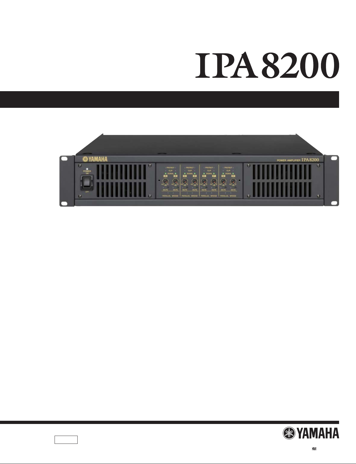
POWER AMPLIFIER
SERVICE MANUAL
011943
PA
200910-265650
■ CONTENTS
SPECIFICATIONS ........................................................................................3
...............................................................................................................4
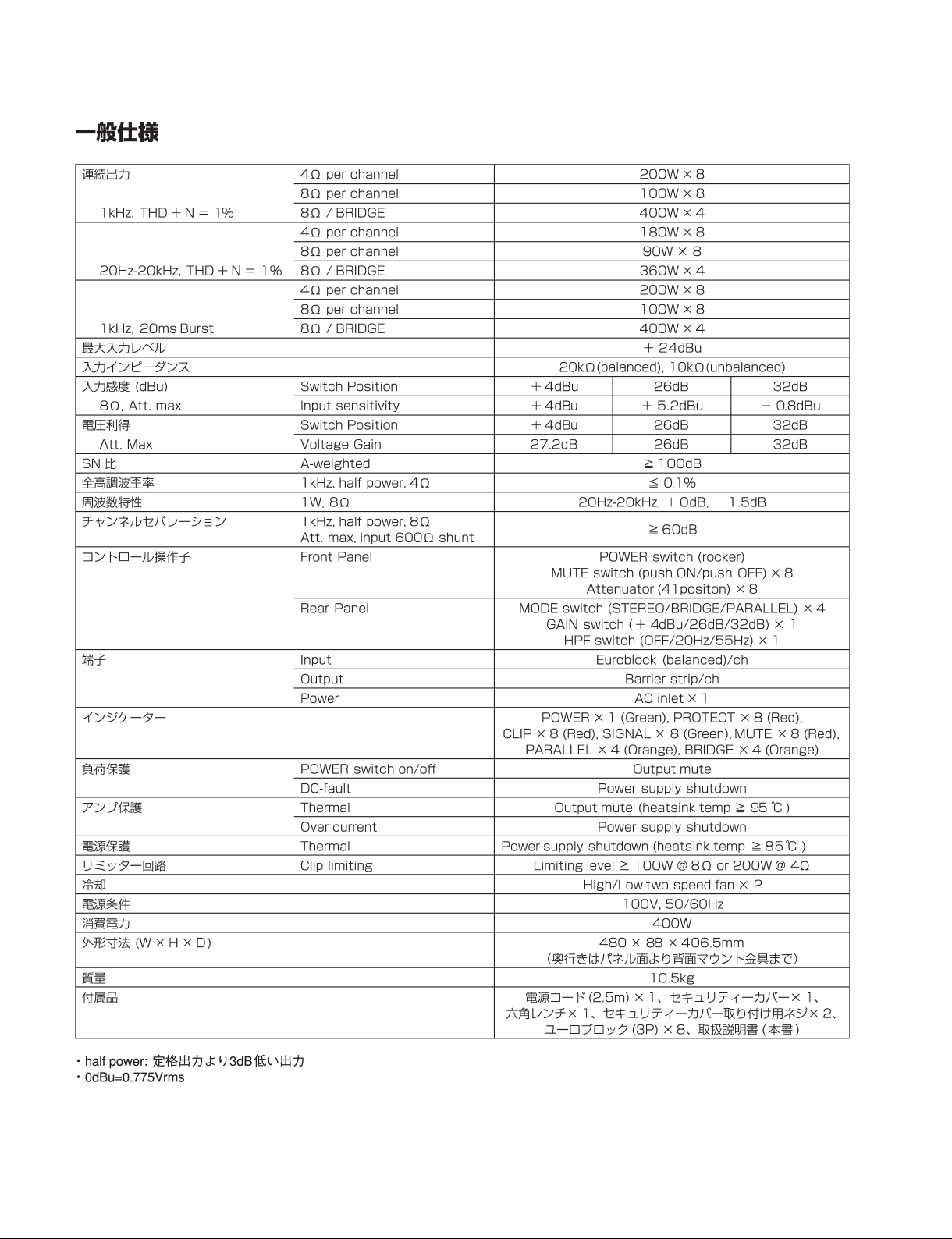
仕様
DIMENSIONS
PANEL LAYOUT
CIRCUIT BOARD LAYOUT
SERVICE PRECAUTIONS
DISASSEMBLY PROCEDURES
IC BLOCK DIAGRAM
CIRCUIT BOARDS
INSPECTIONS ...........................................................................................43
.............................................................................................................45
検査
ADJUSTMENT OF AMP circuit board
PARTS LIST
IC & DIODE FIGURES
WIRING DIAGRAM
BLOCK DIAGRAM
CIRCUIT DIAGRAM
(目次)
(寸法図)
................................................................................5
(パネルレイアウト)
(ユニットレイアウト)
(サービス時の注意)
(IC ブロック図)
(シート基板図)
Copyright (c) Yamaha Corporation. All rights reserved. YMW ´09.11
...........................................................6
........................................7
............................................8
(分解手順)
.............................................................23
............................................... 11
.......................................................22
(AMP シートの調整)
....................46
HAMAMATSU, JAPAN
IPA8200
IMPORTANT NOTICE
This manual has been provided for the use of authorized Yamaha Retailers and their service personnel. It has been assumed that basic service
procedures inherent to the industry, and more specifically Yamaha Products, are already known and understood by the users, and have therefore not been restated.
WARNING: Failure to follow appropriate service and safety procedures when servicing this product may result in personal injury, destruc-
tion of expensive components and failure of the product to perform as specified. For these reasons, we advise all Yamaha
product owners that all service required should be performed by an authorized Yamaha Retailer or the appointed service representative.
IMPORTANT: This presentation or sale of this manual to any individual or firm does not constitute authorization, certification, recognition of
any applicable technical capabilities, or establish a principal-agent relationship of any form.
The data provided is believed to be accurate and applicable to the unit(s) indicated on the cover. The research engineering, and service departments of Yamaha are continually striving to improve Yamaha products. Modifications are, therefore, inevitable and changes in specification are
subject to change without notice or obligation to retrofit. Should any discrepancy appear to exist, please contact the distributor’s Service Division.
WARNING: Static discharges can destroy expensive components. Discharge any static electricity your body may have accumulated by
grounding yourself to the ground bus in the unit (heavy gauge black wires connect to this bus).
IMPORTANT: Turn the unit OFF during disassembly and parts replacement. Recheck all work before you apply power to the unit.
WARNING: This product contains chemicals known to the State of California to cause cancer, or birth defects or other reproductive harm.
DO NOT PLACE SOLDER, ELECTRICAL/ELECTRONIC OR PLASTIC COMPONENTS IN YOUR MOUTH FOR ANY REASON WHAT SO
EVER!
Avoid prolonged, unprotected contact between solder and your skin! When soldering, do not inhale solder fumes or expose eyes to solder/flux
vapor!
If you come in contact with solder or components located inside the enclosure of this product, wash your hands before handling food.
IMPORTANT NOTICE FOR THE UNITED KINGDOM
Connecting the Plug and Cord
WARNING: THIS APPARATUS MUST BE EARTHED
IMPORTANT. The wires in this mains lead are coloured in accordance with the following code:
GREEN-AND-YELLOW: EARTH
BLUE: NEUTRAL
BROWN: LIVE
As the colours of the wires in the mains lead of this apparatus may not correspond with the coloured markings identifying the terminals in your
plug, proceed as follows:
The wire which is coloured GREEN and YELLOW must be connected to the terminal in the plug which is marked by the letter E or by the safety
earth symbol
The wire which is coloured BLUE must be connected to the terminal which is marked with the letter N or coloured BLACK.
The wire which is coloured BROWN must be connected to the terminal which is marked with the letter L or coloured RED.
or colored GREEN or colored GREEN and YELLOW.
WARNING
■
Components having special characteristics are marked and must be replaced with parts having specification equal to those originally
installed.
印の商品は、安全を維持するために重要な部品です。交換する場合は、安全のために必ず指定の部品をご使用ください。
(注意)
2
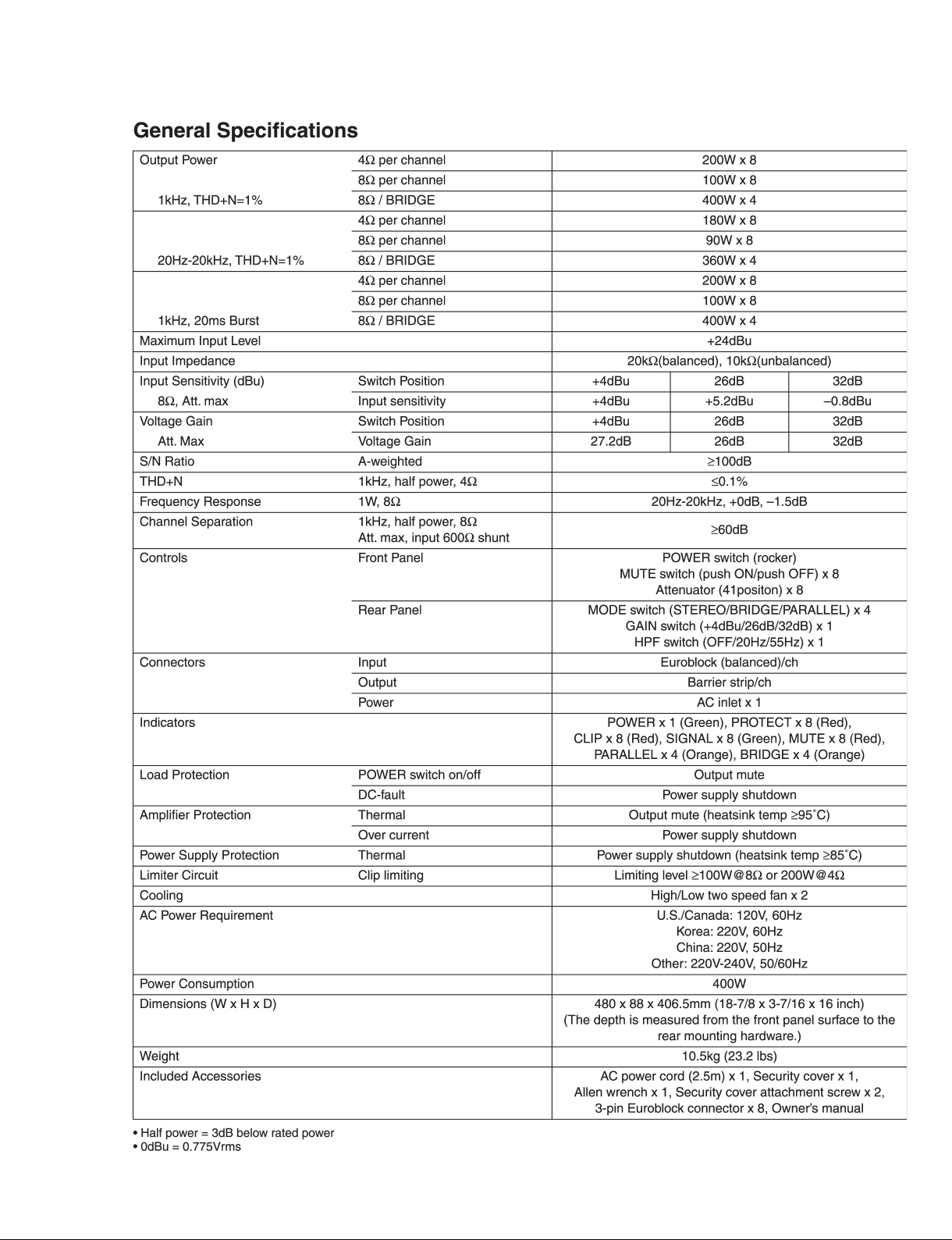
SPECIFICATIONS
■
IPA8200
3
IPA8200
■
仕様
4
IPA8200
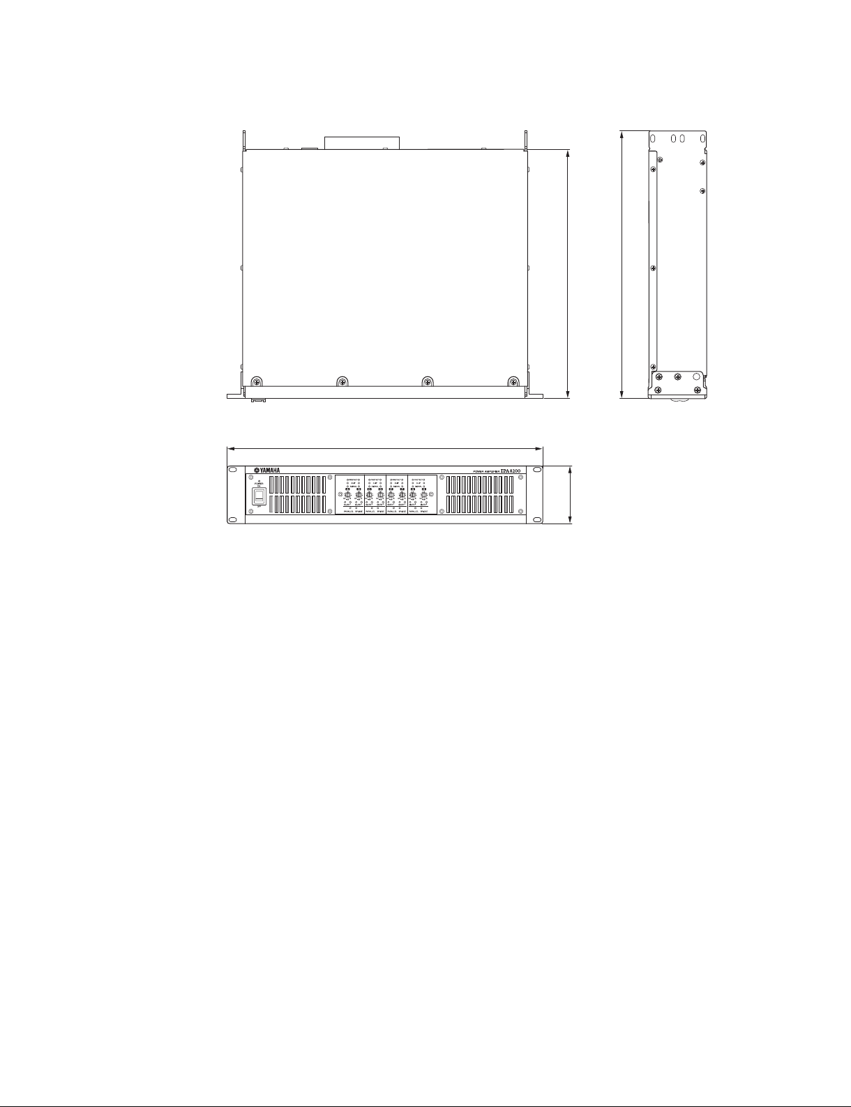
DIMENSIONS
■
(寸法図)
406.5 (16")
377.7 (14-7/8")
480 (18-7/8")
88
(3-7/16")
Unit: mm (inch)
単位 : mm
5
IPA8200
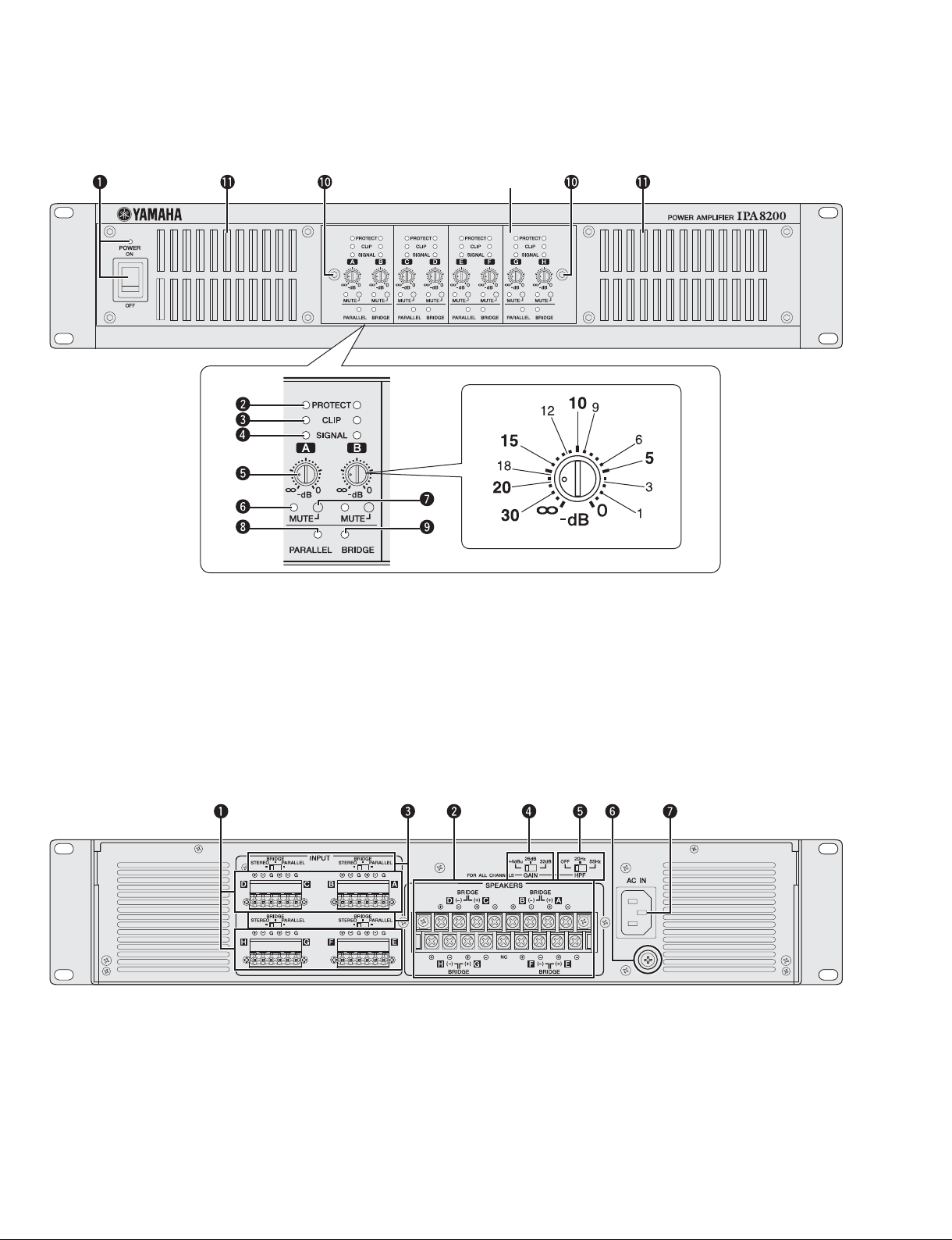
PANEL LAYOUT
■
• Front Panel
(フロントパネル)
(パネルレイアウト)
Security cover
(セキュリティーカバー)
POWER switch and indicator
❶
PROTECT indicator
❷
CLIP indicator
❸
SIGNAL indicator
❹
Attenuator
❺
MUTE indicator
❻
• Rear Panel
INPUT connectors
❶
SPEAKERS connectors
❷
MODE switches
❸
(STEREO mode, BRIDGE mode, PARALLEL mode)
GAIN switch
❹
(+4 dBu, 26 dB, 32 dB)
HPF switch
❺
Ground screw
❻
AC inlet
❼
(リアパネル)
MUTE switch
❼
PARALLEL indicator
❽
BRIDGE indicator
❾
Screw holes for security cover
❿
Air intakes
⓫
POWER スイッチ、インジケーター
❶
❷ PROTECT インジケーター
❸ CLIP インジケーター
❹ SIGNAL インジケーター
❺ アッテネーター
❻ MUTE インジケーター
❶ INPUT 端子
❷ SPEAKERS 端子
❸ MODE スイッチ
(STEREO モード、BRIDGE モード、PARALLEL モード)
❹ GAIN スイッチ
(+4dBu、26dB、32dB)
❺ HPF スイッチ
❻ アース用ネジ
❼ AC インレット
❼ MUTE スイッチ
❽ PARALLEL インジケーター
❾ BRIDGE インジケーター
セキュリティーカバー用ネジ穴
❿
⓫ 吸気口
6
IPA8200
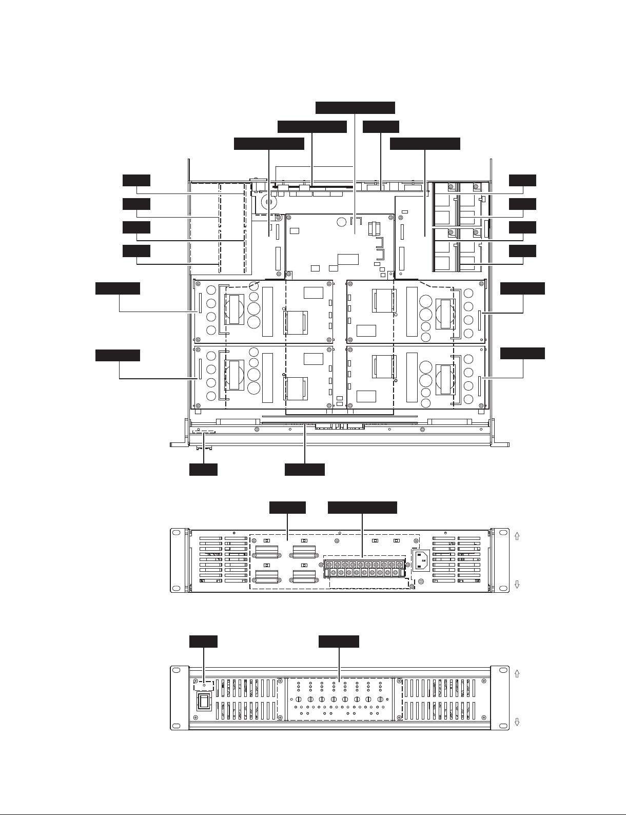
CIRCUIT BOARD LAYOUT
■
MOTHER A–D MOTHER E–H
(CH D)
AMP
(CH C)
AMP
(CH B)
AMP
(CH A)
AMP
POWER
POWER
(CH C–D)
(CH A–B)
(ユニットレイアウト)
INPUT POWER
CONNECTOR
REAR
Rear
AMP
AMP
AMP
AMP
POWER
POWER
(CH H)
(CH G)
(CH F)
(CH E)
(CH G–H)
(CH E–F)
Rear Panel (リアパ ネ ル )
Front Panel (フロントパネ ル)
FRONTLED
REAR
Front
CONNECTOR
Top (上側)
Bottom (下側)
FRONTLED
Top (上側)
Bottom (下側)
7
IPA8200
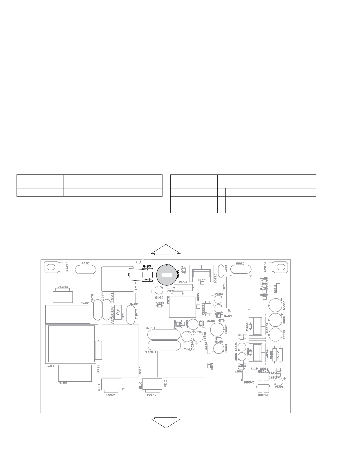
SERVICE PRECAUTIONS
■
(サービス時の注意)
Safety measures
• Some component parts on the INPUT POWER circuit
board and POWER circuit boards maintain a high
voltage even when the power is switched off.
For this reason to avoid an electrical shock, do not touch
the upper metallic part of the following capacitors until
the remaining voltage has discharged.
[Discharging Method]
Before starting the service work, connect discharging
resistors (220 ohms 10W) to the terminals indicated in
the figure below to discharge electricity. (13 points)
The required discharging time is about 10 seconds per
each. Check that the DC voltage between the terminals
measures close to 0 (zero) volts using a multi-meter to
make sure that the discharge is completed.
INPUT POWER circuit board
Capacitors /
コンデンサ
C980
①
Discharging point /
放電箇所
D972: + pin <==> D972: - pin
安全対策
・ INPUT POWER シート、POWER シートの部品の一部
には電源 OFF 状態でも高電圧が残ります。
感電防止のため、残った電圧を放電するまで下記のコ
ンデンサの上部の金属部分に触らないでください。
[放電方法]
修理作業を始める前に、放電抵抗(220 Ω、10 W)を
下図に示す放電用の端子間に接続します。(13 箇所)
放電に必要な時間は各々約 10 秒です。放電完了確認の
ため、端子間電圧がほぼ0(ゼロ)Vであることをテ
スターでチェックします。
POWER circuit board x 4
Capacitors /
コンデンサ
C912, C913
C914
C915
②
③
④
Discharging point /
放電箇所
D904: cathode <==> D901: - pin
Between both terminals of R922
Between both terminals of R923
INPUT POWER cricuit board
220 ohms/10W
1
REAR
D972
C980
FRONT
8
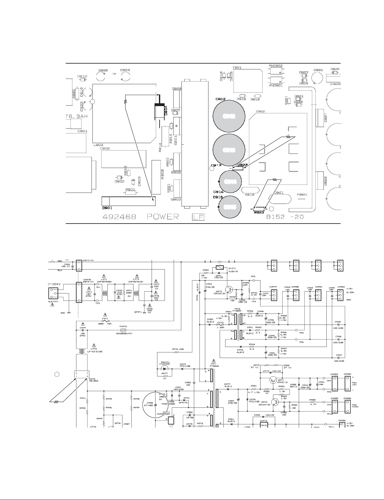
POWER circuit board x 4
220 ohms/10W
2
D904
3
IPA8200
C912
220 ohms/10W
C913
R922
220 ohms/10W
C914
D901
INPUT POWER circuit diagram
1
D972
C915
4
R923
220 ohms/10W
C980
9
IPA8200
POWER circuit diagram x 4
220 ohms/10W
2
D901
D904
3
R922
220 ohms/10W
C912, C913
220 ohms/10W
4
R923
C914
C915
10
IPA8200
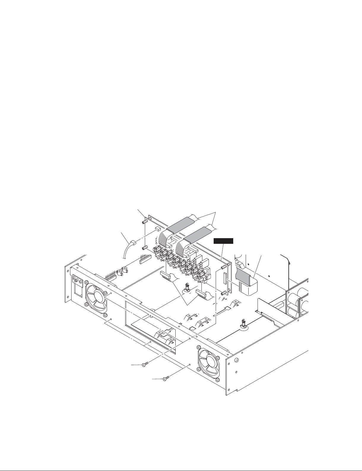
DISASSEMBLY PROCEDURES
■
(分解手順)
1. Top Cover and L Angles (Time required: about 3 minutes)
1-1. Remove the thirteen (13) screws marked [92]. The top
cover can then be removed. (Fig. 1)
1-2. Remove the six (6) screws marked [94]. The two (2) L
angles can then be removed. (Fig. 1)
[92]
[94]
L angle
Lアングル
1. トップカバー、L アングル (所要時間:約 3 分)
1-1. [92]のネジ 13 本を外し、トップカバーを外します。
(図 1)
1-2. [94]のネジ 6 本を外し、L アングル 2 個を外します。
(図 1)
Top cover
トップ カ バ ー
[92]
[94]
[92]
L angle
Lアングル
[92]: BIND HEAD TAPPING SCREW-B 3x8 MFZN2BL (WS522000)
[94]: BIND HEAD TAPPING SCREW-B 4x8 NI-BL (WP183100)
B タイト+ BIND
[92]
[94]
[94]
B タイト+ BIND
Fig. 1
(図 1)
11
IPA8200
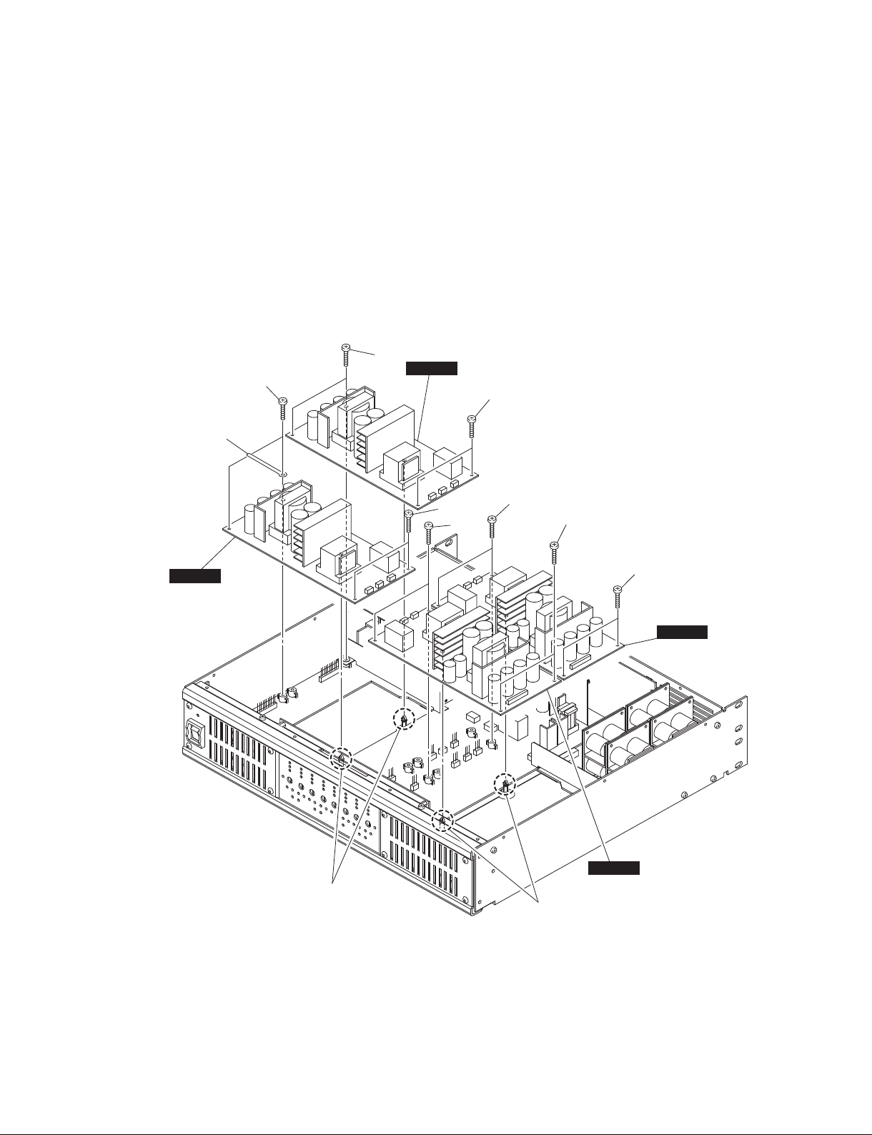
2. AMP Circuit Boards (Time required: about 7 minutes)
2-1. Remove the top cover. (See procedure 1.)
2-2. Remove the two (2) screws marked [62I], the bracket
clip and the shield cover. (Fig. 2)
2-3. Remove the screw marked [62A]. The AMP circuit
board (channel A) can then be removed. (Fig. 2)
2-4. In the same manner, the AMP circuit boards (channel
B, C, D, E, F, G, H) can then be removed. (Fig. 2)
[62I]
[62A]
AMP
(CH B)
[62D]
[62C]
[62B]
AMP
(CH A)
AMP
(CH C)
2. AMP シート (所要時間:約 7 分)
2-1. トップカバーを外します。(1 項参照)
2-2. [62I]のネジ 2 本、ブラケットクリップ、シールド
カバーを外します。(図 2)
2-3. [62A]のネジを外し、AMP シート(チャンネル A)
を外します。(図 2)
2-4. 同様の方法で、AMP シート(チャンネル B、C、D、E、
F、G、H)を外します。(図 2)
Shield cover
シールドカバー
[62I]
Bracket clip
AMP
(CH D)
AMP
[62E]
(CH F)
[62F]
ブラケットクリップ
(CH H)
AMP
[62H]
AMP
(CH G)
[62A]: BIND HEAD TAPPING SCREW-B 3x8 MFZN2BL (WS522000)
[62B]: BIND HEAD TAPPING SCREW-B 3x8 MFZN2BL (WS522000)
[62C]: BIND HEAD TAPPING SCREW-B 3x8 MFZN2BL (WS522000)
[62D]: BIND HEAD TAPPING SCREW-B 3x8 MFZN2BL (WS522000)
[62E]: BIND HEAD TAPPING SCREW-B 3x8 MFZN2BL (WS522000)
[62F]: BIND HEAD TAPPING SCREW-B 3x8 MFZN2BL (WS522000)
[62G]: BIND HEAD TAPPING SCREW-B 3x8 MFZN2BL (WS522000)
[62H]: BIND HEAD TAPPING SCREW-B 3x8 MFZN2BL (WS522000)
[62I]: BIND HEAD TAPPING SCREW-B 3x8 MFZN2BL (WS522000)
(CH E)
AMP
B タイト+ BIND
B タイト+ BIND
B タイト+ BIND
B タイト+ BIND
B タイト+ BIND
B タイト+ BIND
B タイト+ BIND
B タイト+ BIND
B タイト+ BIND
[62G]
12
Fig. 2
(図 2)
IPA8200
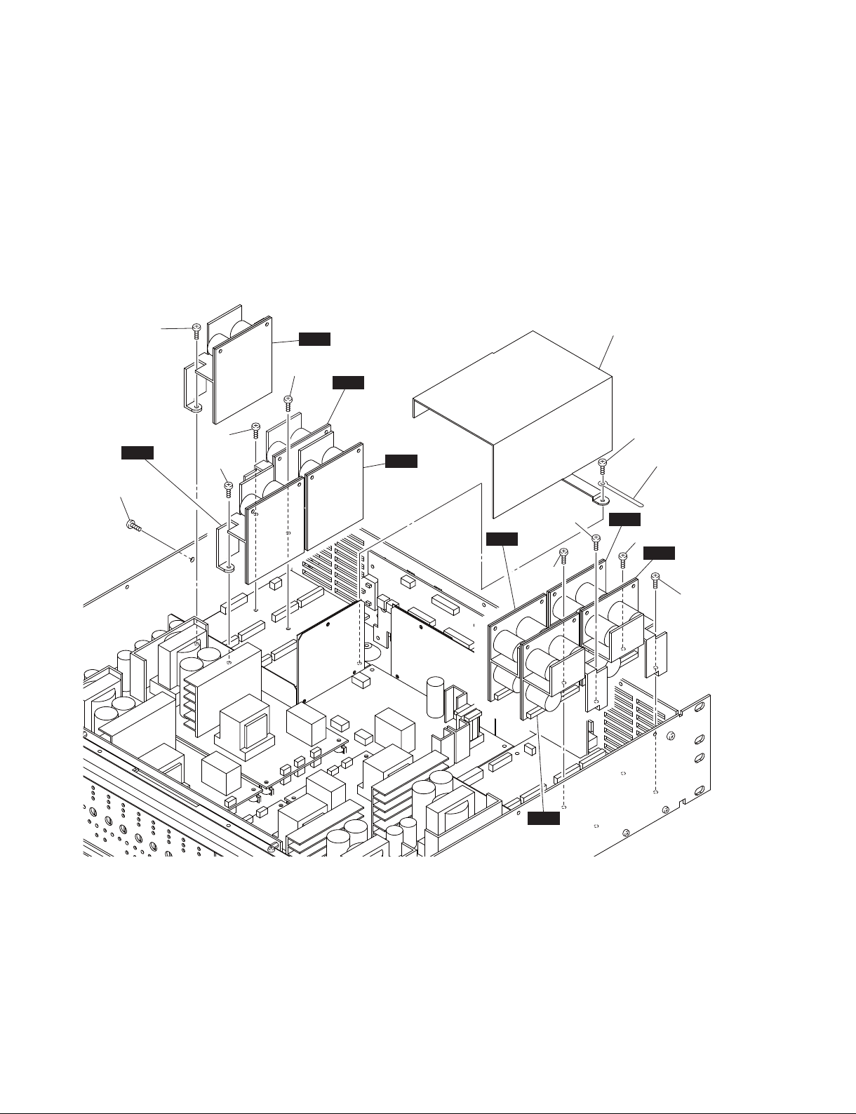
3. POWER Circuit Boards (Time required: about 6 minutes)
3-1. Remove the top cover. (See procedure 1.)
3-2. Remove the four (4) screws marked [76A] and the
bracket clip. Release the spacer. The POWER circuit
board (channel A-B) can then be removed. (Fig. 3)
3-3. Remove the four (4) screws marked [76B]. Release
the spacer. The POWER circuit board (channel C-D)
can then be removed. (Fig. 3)
3-4. In th e same manner, the POWER circuit boards
(channel E-F, G-H) can then be removed. (Fig. 3)
[76B]
[76A]
Bracket clip
ブラケットクリップ
POWER
[76A]
[76C]
3. POWER シート (所要時間:約 6 分)
3-1. トップカバーを外します。(1 項参照)
3-2. [76A]のネジ 4 本、ブラケットクリップを外します。
スペーサーを解除し、POWERシート(チャンネル
A-B)を外します。(図 3)
3-3. [76B]のネジ 4 本を外します。スペーサーを解除し、
POWER シート(チャンネル C-D)を外します。(図 3)
3-4. 同様の方法で、POWER シート(チャンネル E-F、
G-H)を外します。(図 3)
(CH C–D)
[76B]
[76D]
[76C]
POWER
(CH A–B)
Spacers
スペーサー
[76A]: BIND HEAD TAPPING SCREW-B 3.0x16 NI-BL (WT892700)
[76B]: BIND HEAD TAPPING SCREW-B 3.0x16 NI-BL (WT892700)
[76C]: BIND HEAD TAPPING SCREW-B 3.0x16 NI-BL (WT892700)
[76D]: BIND HEAD TAPPING SCREW-B 3.0x16 NI-BL (WT892700)
Spacers
スペーサー
[76D]
POWER
B タイト+ BIND
B タイト+ BIND
B タイト+ BIND
B タイト+ BIND
(CH E–F)
POWER
(CH G–H)
Fig. 3
(図 3)
13
IPA8200
4. MOTHER A-D circuit board (Time required: about 8 minutes)
4-1. Remove the top cover. (See procedure 1.)
4-2. Remove the AMP circuit boards (channel A, B, C, D).
(See procedure 2.)
4-3. Remove the POWER circuit boards (channel A-B,
C-D). (See procedure 3.)
4-4. Remove the screw marked [72A] and the insulation
sheet F. (Fig. 4)
4-5. Remove the screw marked [62B] and the bracket clip.
The MOTHER A-D circuit board can then be removed.
(Fig. 4)
Note: The four (4) PWB spacers are not component
parts of the MOTHER A-D circuit board. When
replacing the MOTHER A-D circuit board, remove
them from old circuit board and install them to
new circuit board.
Connector assembly
束線
Connector assembly
束線
4. MOTHERA-D シート
(所要時間:約 8 分)
4-1. トップカバーを外します。(1 項参照)
4-2. AMP シート(チャンネル A、B、C、D)を外します。
(2 項参照)
4-3. POWER シート(チャンネル A-B、C-D)を外します。
(3 項参照)
4-4. [72A]のネジ、絶縁シート F を外します。(図 4)
4-5. [62B]のネジ、ブラケットクリップを外し、
MOTHERA-D シートを外します。(図 4)
注意:基板スペーサー 4 個は、MOTHERA-D シートの構成
部品ではありません。MOTHERA-D シートを交換す
る際には、基板スペーサー 4 個を古いシートから外
して。新しいシートに取り付けてください。
[62B]
Bracket clip
ブラケットクリップ
Insulation sheet F
絶縁シートF
Connector assembly
束線
[72A]
PWB spacers
基板スペーサー
[62B]: BIND HEAD TAPPING SCREW-B 3x8 MFZN2BL (WS522000)
[72A]: BIND HEAD TAPPING SCREW-B 3x8 MFZN2BL (WS522000)
MOTHER A–D
B タイト+ BIND
B タイト+ BIND
14
Fig. 4
(図 4)
IPA8200
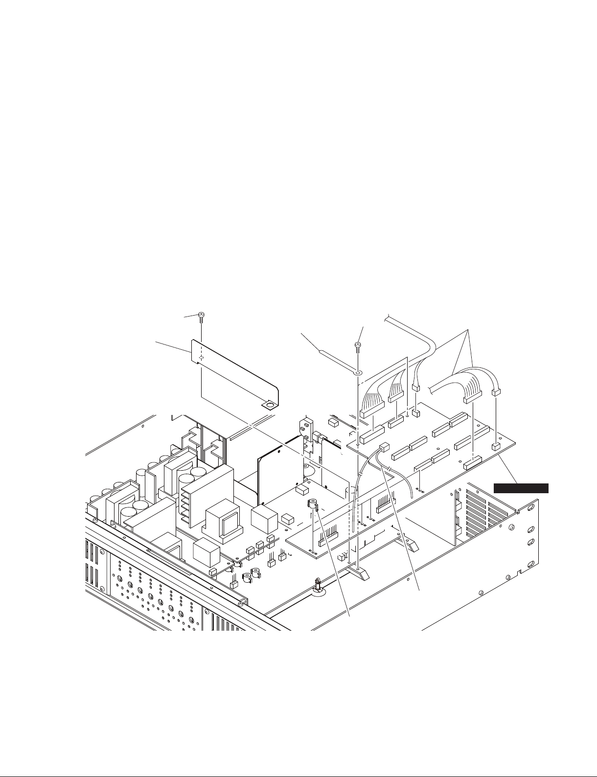
5. MOTHER E-H circuit board (Time required: about 8 minutes)
5-1. Remove the top cover. (See procedure 1.)
5-2. Remove the AMP circuit boards (channel E, F, G, H).
(See procedure 2.)
5-3. Remove the POWER circuit boards (channel E-F,
G-H). (See procedure 3.)
5-4. Remove the screw marked [72B] and the insulation
sheet E. (Fig. 5)
5-5. Remove the two (2) screws marked [62C] and the two
(2) bracket clips. The MOTHER E-H circuit board can
then be removed. (Fig. 5)
Note: The four (4) PWB spacers are not component
parts of the MOTHER E-H circuit board. When
replacing the MOTHER E-H circuit board, remove
them from old circuit board and install them to
new circuit board.
[72B]
Insulation sheet E
絶縁シートE
Bracket clip
ブラケットクリップ
5. MOTHERE-H シート
(所要時間:約 8 分)
5-1. トップカバーを外します。(1 項参照)
5-2. AMP シート(チャンネル E、F、G、H)を外します。
(2 項参照)
5-3. POWER シート(チャンネル E-F、G-H)を外します。
(3 項参照)
5-4. [72B]のネジ、絶縁シート E を外します。(図 5)
5-5. [62C]のネジ 2 本、ブラケットクリップ 2 個を外し、
MOTHERE-H シートを外します。(図 5)
注意:基板スペーサー 4 個は、MOTHERE-H シートの構成
部品ではありません。MOTHERE-H シートを交換す
る際には、基板スペーサー 4 個を古いシートから外
して。新しいシートに取り付けてください。
[62C]
Connector assembly
束線
Connector assembly
束線
PWB spacers
基板スペーサー
[62C]: BIND HEAD TAPPING SCREW-B 3x8 MFZN2BL (WS522000)
[72B]: BIND HEAD TAPPING SCREW-B 3x8 MFZN2BL (WS522000)
Fig. 5
(図 5)
MOTHER E–H
B タイト+ BIND
B タイト+ BIND
15
IPA8200
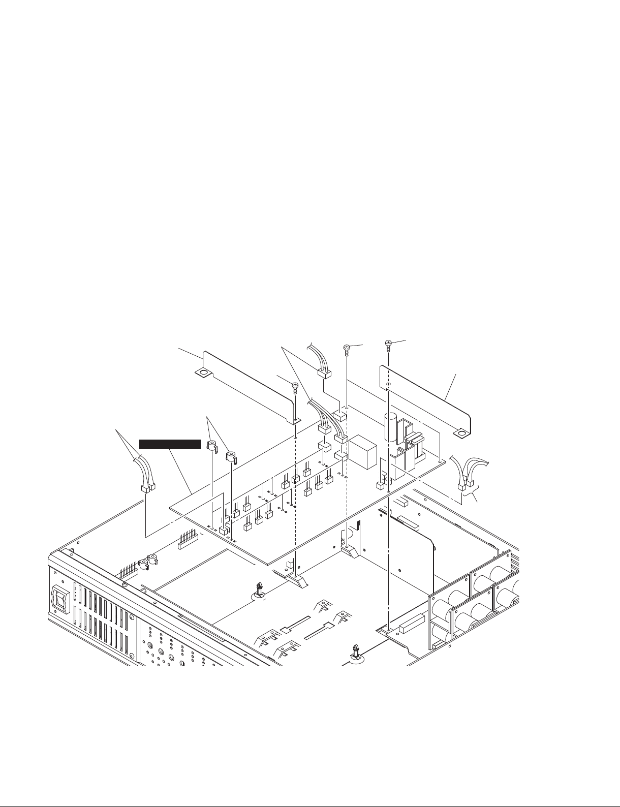
6. INPUT POWER Circuit Board (Time required: about 9 minutes)
6-1. Remove the top cover. (See procedure 1.)
6-2. Remove all the POWER circuit boards.
(See procedure 3.)
6-3. Remove the screw marked [72A] and the insulation
sheet F. (Fig. 6)
6-4. Remove the screw marked [72B] and the insulation
sheet E. (Fig. 6)
6-5. Remove the two (2) screws marked [43]. (Fig. 6)
6-6. Disconnect all the connector assemblies from the
INPUT POWER circuit board. The INPUT POWER
circuit board can then be removed. (Fig. 6)
Note: The eight (8) PWB spacers are not component
parts of the INPUT POWER circuit board. When
replacing the INPUT POWER circuit board, remove
them from old circuit board and install them to
new circuit board.
Insulation sheet F
絶縁シートF
Connector assembly
束線
[72A]
6. INPUTPOWER シート
(所要時間:約 9 分)
6-1. トップカバーを外します。(1 項参照)
6-2. すべての POWER シートを外します。(3 項参照)
6-3. [72A]のネジ、絶縁シート F を外します。(図 6)
6-4. [72B]のネジ、絶縁シート E を外します。(図 6)
6-5. [43]のネジ 2 本を外します。(図 6)
6-6. INPUTPOWER シートからすべての束線を外し、
INPUTPOWER シートを外します。(図 6)
注意:8 個の基板スペーサーは、INPUTPOWER シートの
構成部品ではありません。INPUTPOWER シートを
交換する際には、古いシートから基板スペーサーを
取り外して新しいシートへ取り付けてください。
[43]
[72B]
Insulation sheet E
絶縁シートE
Connector assembly
束線
INPUT POWER
PWB spacers
基板スペーサー
Connector assembly
束線
16
[43]: BIND HEAD TAPPING SCREW-B 3x8 MFZN2BL (WS522000)
[72A]: BIND HEAD TAPPING SCREW-B 3x8 MFZN2BL (WS522000)
[72B]: BIND HEAD TAPPING SCREW-B 3x8 MFZN2BL (WS522000)
Fig. 6
(図 6)
B タイト+ BIND
B タイト+ BIND
B タイト+ BIND
IPA8200
7. REAR Circuit Board (Time required: about 5 minutes)
7-1. Remove the top cover. (See procedure 1.)
7-2. Remove the eight (8) screws marked [25] and the four
(4) screws marked [24]. (Fig. 7)
7-3. Disconnect all the connector assemblies from the
REAR circuit board. The REAR circuit board can
then be removed together with the four (4) hexagonal
spacers and four (4) screws. (Fig. 7)
Note: The four (4) hexagonal spacers and four (4)
screws are not component parts of the REAR
circuit board. When replacing the REAR circuit
board, remove them from old circuit board and
install them to new circuit board.
Hexagonal spacers
六角スペーサー
7. REAR シート (所要時間:約 5 分)
7-1. トップカバーを外します。(1 項参照)
7-2. [25]のネジ8本、[24]のネジ 4 本を外します。(図 7)
7-3. REAR シートからすべての束線を外し、REAR シー
トを六角スペーサー 4 本、ネジ 4 本と共に外します。
(図 7)
注意:六角スペーサー 4 本、ネジ 4 本は、REAR シートの
構成部品ではありません。REAR シートを交換する
際には、古いシートから六角スペーサー 4 本、ネジ 4
本を外して、新しいシートに取り付けてください。
[24]
REAR
Screws
ネジ
Connector assemblies
束線
[24]
[25]
[25]
Screws
ネジ
[24]: BIND HEAD SCREW 3x6 MFZN2B3 (WS522500)
[25]: PAN HEAD SCREW M2.6x6 NI-BL (WS522400)
Fig. 7
(図 7)
小ネジ+ BIND
小ネジ+ PAN
17
IPA8200
8. CONNECTOR Circuit Board (Time required: about 13 minutes)
8-1. Remove the top cover. (See procedure 1.)
8-2. Remove all the POWER circuit boards.
(See procedure 3.)
8-3. Remove the INPUT POWER circuit board.
(See procedure 6.)
8-4. Remove the REAR circuit board. (See procedure 7.)
8-5. Remove the two (2) screws marked [13]. (Fig. 8)
8-6. Disconnect the connector assemblies from the
CONNECTOR circuit board. The CONNECTOR circuit
board can then be removed together with the two (2)
bracket terminals and two (2) screws. (Fig. 8)
Note: The two (2) bracket terminals and two (2) screws
are not component parts of the CONNECTOR
circuit board. When replacing the CONNECTOR
circuit board, remove them from old circuit board
and install them to new circuit board.
9. AC Inlet Assembly
(Time required: about 6 minutes)
9-1. Remove the top cover. (See procedure 1.)
9-2. Remove the AMP circuit board (channel D).
(See procedure 2.)
9-3. Remove the screw marked [15], and remove the lug
terminal of the AC inlet assembly and the toothed lock
washer. (Fig. 8)
9-4. Disconnect the AC inlet connector assembly connector
from the INPUT POWER circuit board. (Fig. 8)
9-5. Release the two (2) hooks of the AC inlet. The AC inlet
assembly can then be removed. (Fig. 8)
8. CONNECTOR シート (所要時間:約 13 分)
8-1. トップカバーを外します。(1 項参照)
8-2. すべての POWER シートを外します。(3 項参照)
8-3. INPUTPOWER シートを外します。(6 項参照)
8-4. REAR シートを外します。(7 項参照)
8-5. [13]のネジ 2 本を外します。(図 8)
8-6. CONNECTOR シートからすべての束線を外し、
CONNECTOR シートをブラケットターミナル 2 個、
ネジ 2 本と共に外します。(図 8)
注意:ブラケットターミナル2個、ネジ2本は、
CONNECTOR シートの構成部品ではありません。
CONNECTOR シートを交換する際には、古いシー
トからブラケットターミナル 2 個、ネジ 2 本を外し、
新しいシートに取り付けます。
9. AC インレット Ass'y
(所要時間:約 6 分)
9-1. トップカバーを外します。(1 項参照)
9-2. AMP シート(チャンネル D)を外します。(2 項参照)
9-3. [15]のネジを外し、AC インレット Ass'y のラグ端
子と歯付ワッシャーを外します。(図 8)
9-4. INPUTPOWER シートから、AC インレット Ass'y
の束線を外します。(図 8)
9-5. AC インレットの 2 ヶ所のフックを解除し、AC イン
レット Ass'y を外します。(図 8)
AC inlet assembly
ACインレットAss'y
Connector assembly
束線
Hook
フック
[15]
Lug terminal
ラグ端 子
18
CONNECTOR
Screws
ネジ
Bracket terminal
ブラケットターミナ ル
[13]: BIND HEAD TAPPING SCREW-B 3x8 MFZN2BL (WS522000)
[15]: BIND HEAD SCREW M4x8 CR3 BLACK (WS522700)
Fig. 8
(図 8)
小ネジ+ BIND
B タイト+ BIND
Toothed lock washer
[13]
歯付ワッシャー
IPA8200
10. Front Panel, Deco Panel Assembly and Power
Switch Assembly
(Time required: about 8 minutes)
10-1. Remove the top cover. (See procedure 1.)
10-2. Disconnect the wires of the power switch assembly
from the INPUT POWER circuit board. (Fig. 9)
10-3. Remove the six (6) screws marked [34]. The front
panel can then be removed together with the deco
panel assembly and power switch assembly. (Fig. 9)
10-4. Remove the eight (8) screws marked [84]. The deco
panel assembly can then be removed together with
the power switch assembly from the front panel. (Fig. 9)
10-5. Release the two (2) hooks of the power switch. The
power switch assembly and the SW escutcheon can
then be removed from the deco panel assembly. (Fig. 9)
Note: When installing the power switch assembly, set
the red/black cables to the left side and the yellow/
white cables to the right side in order to set its
ON/OFF position normal.
Front panel
フロントパネル
[34]
10. フロントパネル、DECO パネル Ass'y、電源ス イッチ Ass'y
(所要時間:約 8 分)
10-1. トップカバーを外します。(1 項参照)
10-2. 電源スイッチの線材を、INPUTPOWER シートから
外します。(図 9)
10-3.[34]のネジ 6 本を外します。フロントパネルを、
DECO パネル Ass'y、電源スイッチ Ass'y と共に外し
ます。(図 9)
10-4.[84]のネジ 8 本を外し、DECO パネル Ass'y を電源
スイッチ Ass'y と共にフロントパネルから外します。
(図 9)
10-5. 電源スイッチのフック 2 個所を解除し、電源スイッ
チ Ass'y と SW エスカッションを DECOパネル
Ass'y から外します。(図 9)
注意:電源スイッチを取り付ける際には、スイッチの ON/
OFF 位置を正しくするために、赤 / 黒の線材を左側に、
黄 / 白の線材を右側に位置させます。
DECO panel assembly
DECOパネルAss'y
[84]
SW escutcheon
S W エ ス カッション
Hook
フック
Hook
フック
Power switch assembly
電源スイッチAss'y
Connector assembly
束線
Black
黒
Red
赤
White
白
Yellow
黄
[84]
[34]
[34]: BIND HEAD TAPPING SCREW-B 3x8 MFZN2BL (WS522000)
[84]: HEXAGONAL TAPPING SCREW-B 3x8 NI-BL (WP927800)
Fig. 9
(図 9)
六角穴付 B タイトネジ
B タイト+ BIND
19
IPA8200
11. Fans (Time required: about 8 minutes)
11-1. Remove the top cover. (See procedure 1.)
11-2. Remove the front panel together with the deco panel
assembly and power switch assembly.
(See procedure 10.)
Left Fan
11-3. Disconnect the left fan connector assembly from the
INPUT POWER circuit board. (Fig. 10)
11-4. Remove the four (4) screws marked [3A] and four (4)
hexagonal nuts marked [4A]. The left fan can then be
removed. (Fig. 10)
Right Fan
11-5. Disconnect the right fan connector assembly from the
INPUT POWER circuit board. (Fig. 10)
11-6. Remove the four (4) screws marked [3B] and four (4)
hexagonal nuts marked [4B]. The right fan can then be
removed. (Fig. 10)
12. LED Circuit Board (Time required: about 5 minutes)
12-1. Remove the top cover. (See procedure 1.)
12-2. Remove the front panel together with the deco panel
assembly and power switch assembly.
(See procedure 10.)
12-3. Remove the two (2) screws marked [6]. (Fig. 10)
12-4. Disconnect the connector assembly from the LED
circuit board. The LED circuit board can then be
removed. (Fig. 10)
11. ファン(所要時間:約 8 分)
11-1. トップカバーを外します。(1 項参照)
11-2. フロントパネルを DECO パネル Ass'y、電源スイッ
チ Ass'y と共に外します。(10 項参照)
左側のファン
11-3. 左側のファンの線材を INPUT シートから外します。
(図 10)
11-4.[3A]のネジ 4 本、[4A]の六角ナット 4 個を外し、
左側のファンを外します。(図 10)
右側のファン
11-5. 右側のファンの束線を INPUT シートから外します。
(図 10)
11-6.[3B]のネジ 4 本、[4B]の六角ナット 4 個を外し、
右側のファンを外します。(図 10)
12. LED シート (所要時間:約 5 分)
12-1. トップカバーを外します。(1 項参照)
12-2. フロントパネルを DECO パネル Ass'y、電源スイッ
チ Ass'y と共に外します。(10 項参照)
12-3.[6]のネジ 2 本を外します。(図 10)
12-4. LED シートから束線を外し、LED シートを外します。
(図 10)
Connector assembly
束線
[6]
LED
[3A]
[3A]
[3A]: PAN HEAD SCREW M4x35 CR3 BLACK (WS522200)
[3B]: PAN HEAD SCREW M4x35 CR3 BLACK (WS522200)
[4A]: HEXAGONAL NUT M4.0 CR3 (AAX61890)
[4B]: HEXAGONAL NUT M4.0 CR3 (AAX61890)
[6]: BIND HEAD TAPPING SCREW-B 3x8 MFZN2BL (WS522000)
Left fan
左側のファン
[3B]
[4A]
Connector assembly
束線
[3B]
小ネジ+ PANSP
小ネジ+ PANSP
フランジ付き六角ナット
フランジ付き六角ナット
[4B]
Right fan
右側のファン
B タイト+ BIND
20
Fig. 10
(図 10)
IPA8200
13. FRONT Circuit Board Assembly
(Time required: about 15 minutes)
13-1. Remove the top cover. (See procedure 1.)
13-2. Remove all the POWER circuit boards.
(See procedure 3.)
13-3. Remove the INPUT POWER circuit board.
(See procedure 6.)
13-4. Remove the front panel together with the deco panel
assembly and the power switch assembly.
(See procedure 10.)
13-5. Disconnect all the connector assemblies from the
FRONT circuit board. (Fig. 11)
13-6. Remove the six (6) screws marked [32]. The FRONT
circuit board assembly can then be removed together
with the . (Fig. 11)
Note: For details of the FRONT circuit board assembly,
see parts list page xx.
FRONT circuit board assembly
FRONTシートAss'y
13. FRONT シート Ass'y
(所要時間:約 15 分)
13-1. トップカバーを外します。(1 項参照)
13-2. すべての POWER シートを外します。(3 項参照)
13-3. INPUTPOWER シートを外します。(6 項参照)
13-4. フロントパネルを DECO パネル Ass'y、電源スイッ
チ Ass'y と共に外します。(10 項参照)
13-5. すべての束線を、FRONT シートから外します。
(図 11)
13-6.[32]のネジ 6 本を外し、FRONT シートAss'y を外
します。(図 11)
注意:FRONT シート Ass'y の詳細については、パーツリス
ト xx ページを参照してください。
Connector assembly
束線
Connector assembly
束線
[32]
FRONT
FFC cable
フラットケーブル
Connector assembly
束線
[32]
[32]: BIND HEAD SCREW 3x6 MFZN2B3 (WS522500)
Fig. 11
(図 11)
小ネジ+ BIND
21
IPA8200
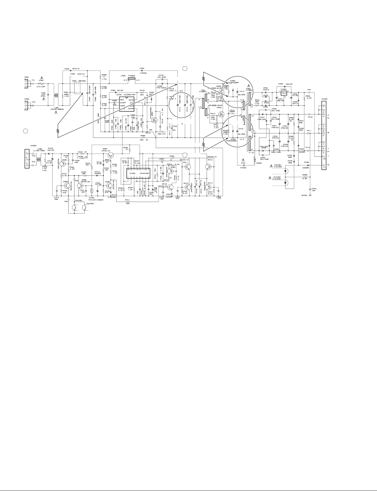
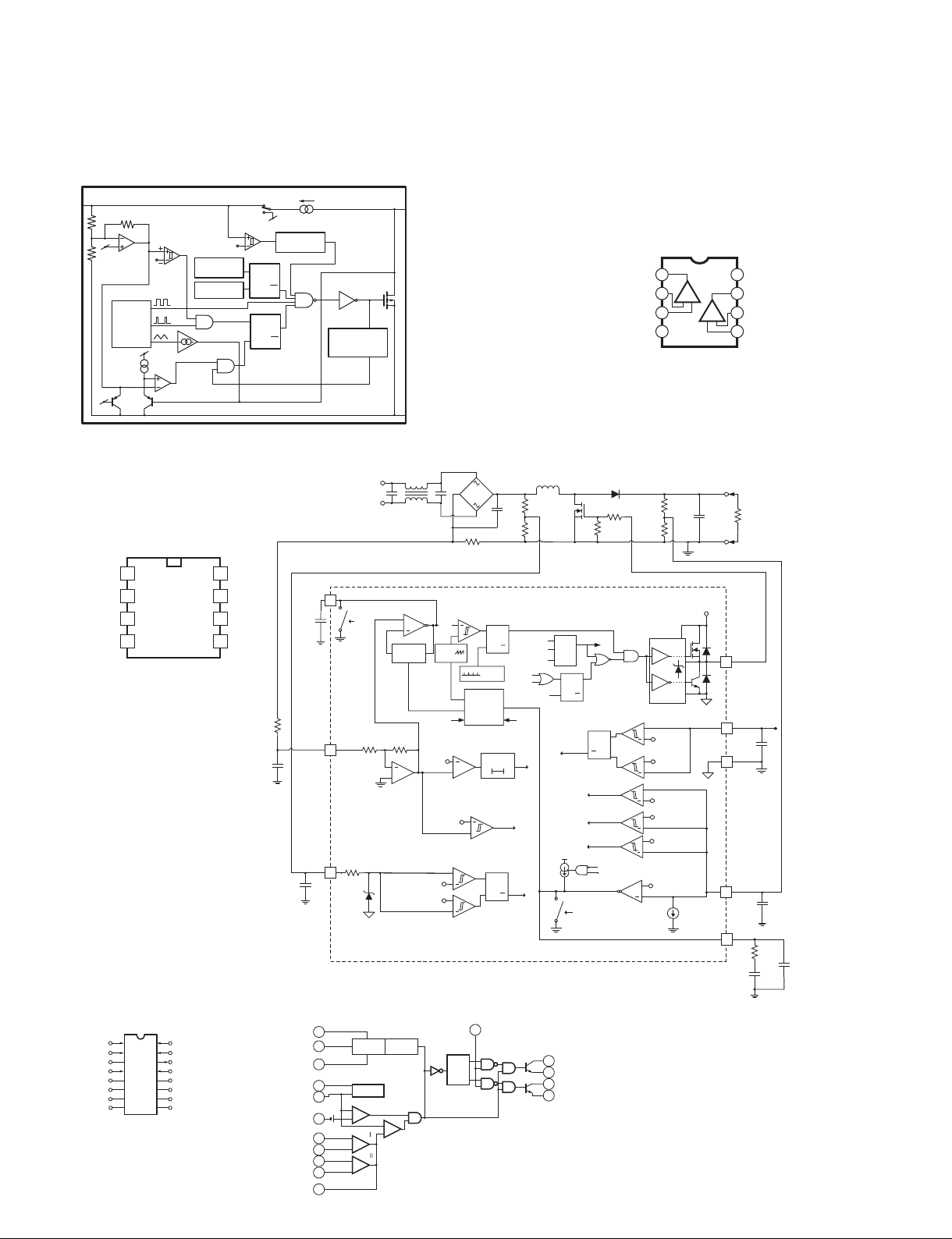
IC BLOCK DIAGRAM
■
rMIP2E4DMY (YA883A0)
IPD
INPUT POWER: IC971
1
Control
For control over
light load detecting
Air lamp
Oscillator
Max Duty
Sawtooth
Overcurrent
protection
Clock
intermittent oscillation
Overheat
protection
V-I converter
Slope
compensation
Drain current
for detection
Restart
trigger
rUCC28019DR (YA885A0)
PFC Controller
POWER: IC901
1
2
3
4
GND
ICOMP
ISENSE
VINS
GATE
VCC
VSENSE
VCOMP
8
7
6
5
r61$(45"5 (X8569A0)
SWR Controller
POWER: IC902
Non-Inv. Input
Feed-Back
Dead-Time
Inv. Input
Control
GND
1
2
3
4
5
CT
6
RT
7
C1
8
16
15
14
13
12
11
10
9
Non-Inv. Input
Inv. Input
Ref Out
Output Control
VCC
C2
E2
E1
22
R
C
SRQ
S
R
ISENSE
ISENSE
Non-Inv. Input
Non-Inv. Input
(IC ブロック図)
Start-up constant current
Internal power supply
Timer intermittent
operation circuit
Q
Q
Q
ICOMP
C
ICOMP
ISENSE
VINS
C
VINS
V
CC
12
Ref Out
14
GND
RT
CT
Dead-Time
Control
Inv. Input
16
Inv. Input
15
Feed-Back
Gate driver
7
6
5
4
1
2
3
Blanking pulse
generation
circuit in on-state
2
3
20k
4
5V
Power
MOSFET
2
LINE
INPUT
Current
Amplifier
FAULT
GAIN
M
40k 40k
+
Input Brown-Out Protection
VIN
VIN
BROWNOUT_th
Reference
Low Voltage
Regulator
Stop
Oscillator
Dead Time
Comparator
+
+
-
EA
PWM
+
Comparator
-
EA
+
-
3
1
-1x
(IBOP)
Drain
Source
EMI Filter
+
gmi
ENABLE_th
ICOMP
+
PWM
RAMP
M
2
Peak Current Limit (PCL)
V
PCL
1.08V
+
Soft Over Current (SOC)
V
0.73V
SOC
+
1.5V
+
0.82V
T /
R
SENSE
M
M
SOC
F
F
Bridge
Rectifier
PWM
Comparator
K
2
1
+
13
+–
R
VINS1
C
IN
R
VINS2
(s)
PC
SQ
QR
Min Off Time
65kHz
Oscillator
VCOMP
EDR
300ns
Leading Edge
Blanking
SOC
SQ
QR
Output Control
r/+..%5& (AAX6275)
Operational Amplifier
REAR: IC11, 31, 51, 71
FRONT: IC101, 102, 202, 301, 302, 402,
IC501, 502, 602, 701, 702, 802
MOTHER A-D: IC1101, 1301
MOTHER E-H: IC1501, 1701
Output A +V
Inverting
Input A
Non-Inverting
Input A
-DC Voltage Supply
L
BST
Q
IBOP
Fault
UVLO
Logic
OLP
PCL
OVP
Clock
PCL
IBOP
C1
8
E1
9
11
C2
10
E2
BST
SQ
UVLO
10k
QR
FAULT
D
R
Fault
SQ
QR
OVP
OLP/STANDBY
EDR
SS
EDR
BST
GATE
Gate Driver
UVLO
Voltage Error
Amplifier
R
FB1
R
FB2
+
+
+
+
+
+
gmv
1
2
3
4-V
C
OUT
Pre-Driveand
Clamp Circuit
VCC
ON
10.5V
VCC
OFF
9.5V
OVERVOLTAGE
5.25V
OLP/STANDBY
0.82V
UNDERVOLTAGE
4.75V
5V
100μA
+-
+-
VCC
V
OUT
8
7
1
6
5
8
7
6
5
GATE
VCC
GND
VSENSE
C
VSENSE
VCOMP
R
VCOMP
C
VCOMP
R
C
+DC Voltage
Supply
Output B
Inverting
Input B
Non-Inverting
Input B
LOAD
Auxilary
Supply
VCC
C
VCOMP-P

IPA8200
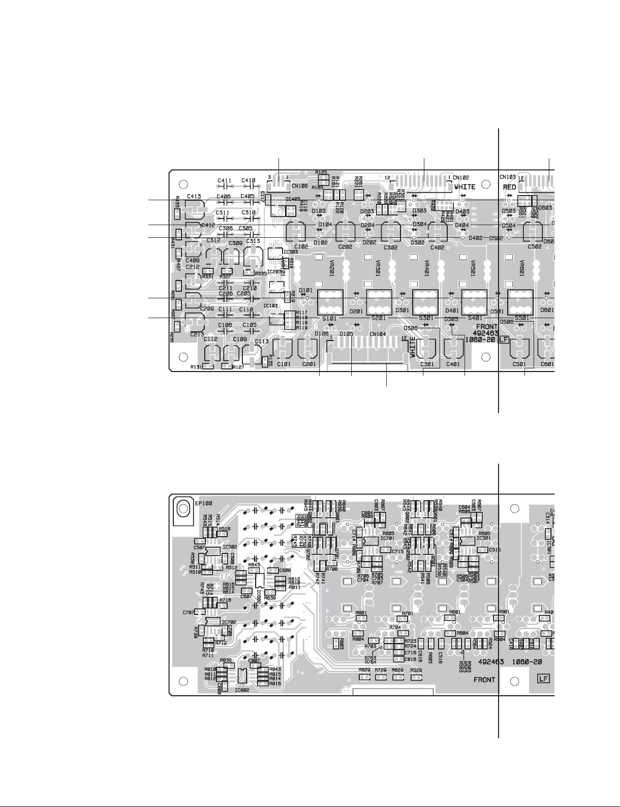
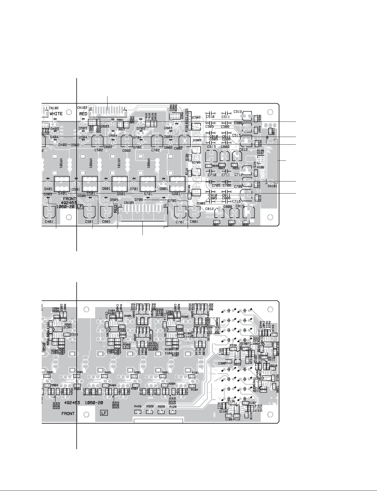
■ CIRCUIT BOARDS
(シート基板図)
CONTENTS
• AMP Circuit Board (4205-20) ..............................42
• CONNECTOR Circuit Board (5258-20) ..............................42
• FRONT Circuit Board (1060-20) ..............................26
• INPUT POWER Circuit Board (9077-20) .............................. 36
• LED Circuit Board (5258-20) .............................. 42
• MOTHER A–D Circuit Board (5258-20) ..............................28
• MOTHER E–H Circuit Board (7483-20) .............................. 32
• POWER Circuit Board (8152-20) ..............................40
• REAR Circuit Board (2029-20) ..............................24
Note: See parts list for details of circuit board component parts.
注: シートの部品詳細はパーツリストをご参照ください。
(目次)
23
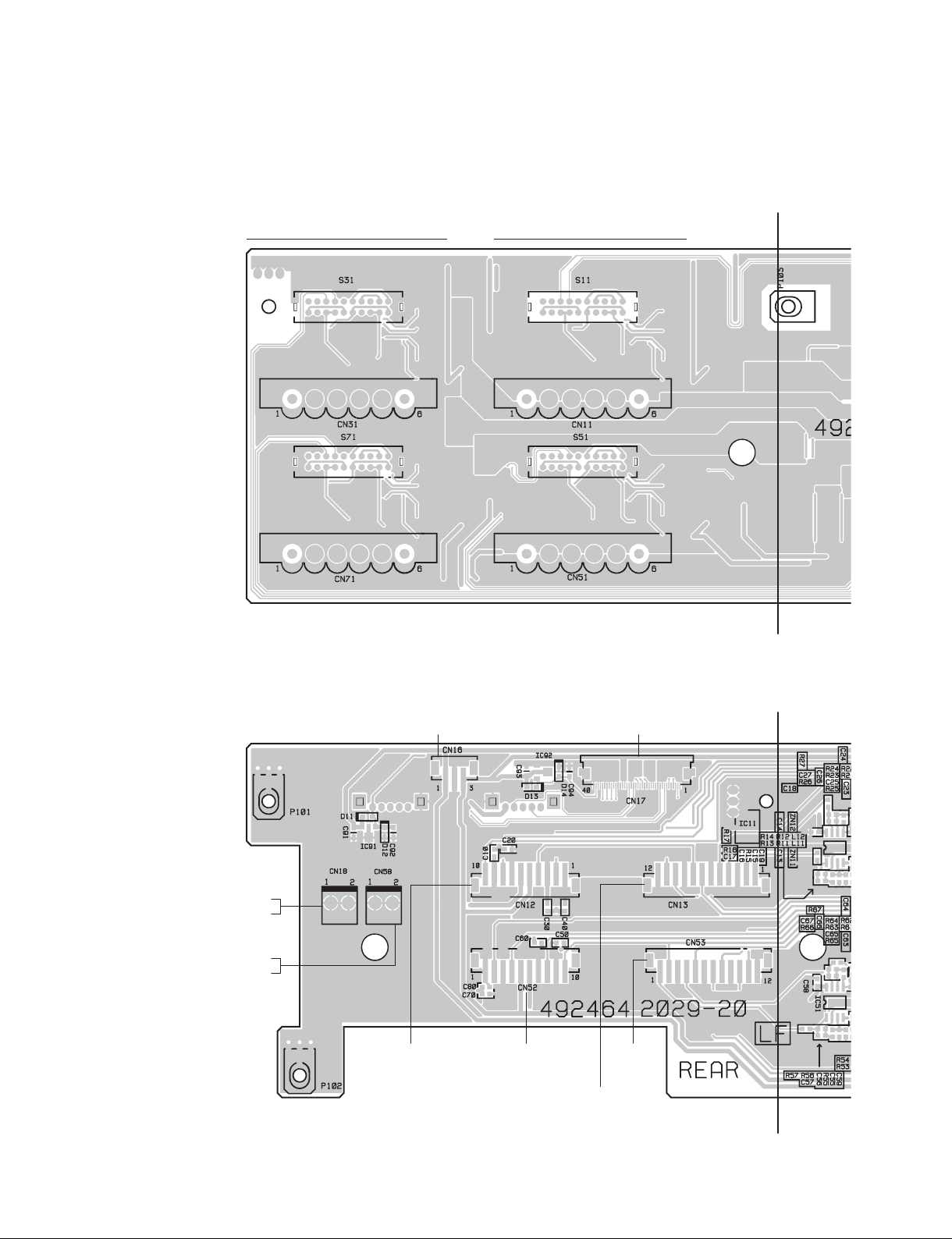
IPA8200
• REAR Circuit Board
STEREO
BRIDGE
PARALLEL
INPUT
STEREO
BRIDGE
A
PARALLEL
+ -G+ -G
STEREO
BRIDGE
+ -G+ -G
Component side
PARALLEL
(部品側)
to INPUT POWER
CD
GH
CN986
+ -G+ -G
STEREO
BRIDGE
+ -G+ -G
PARALLEL
to FRONT
CN101
AB
EF
A'
B
24
to MOTHER A-D PGND1 BLACK
to MOTHER A-D PGND3 WHITE
to MOTHER E-H PGND5 BLACK
to MOTHER E-H PGND7 WHITE
Pattern side
to MOTHER A-D
CN1107
(パターン側)
to MOTHER E-H
CN1507
to FRONT
CN105
to FRONT
CN104
B'
492464
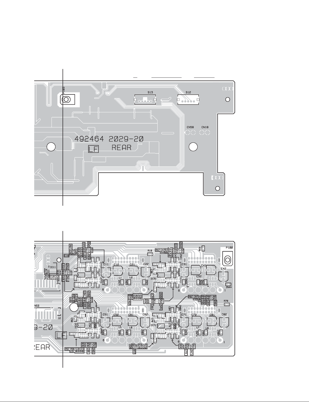
• REAR Circuit Board
A
GAINFOR ALL CHANNELS HPF
26dB
+4dBu 32dB
20Hz
OFF 55Hz
IPA8200
A'
B
Component side
(部品側)
492464
B'
Pattern side
(パターン側)
25
E
B
IPA8200
• FRONT Circuit Board
A
PROTECT
CLIP
SIGNAL
MUTE LED
MUTE
Component side
to LED
CN107
(部品側)
to MOTHER A-D
CN1106
ABCDEF
PARALLEL
BRIDGE
to REAR
PARALLEL BRIDGE PARALLEL
CN13
to MOTH
CN15
A'
Pattern side
(パターン側)
B
B'
26
492463
• FRONT Circuit Board
A
IPA8200
-D
-D
EFGH
BRIDGE PARALLEL BRIDGE PARALLEL BRIDGE
to MOTHER E-H
to MOTHER E-H
CN1506
CN1506
to REAR
to REAR
CN53
CN53
A'
Component side
(部品側)
PROTECT
CLIP
SIGNAL
to REAR
to REAR
CN17
CN17
MUTE LED
MUTE
B
B'
Pattern side
(パターン側)
Pattern side
(パターン側)
492463
27
P
1
IPA8200
• MOTHER A-D Circuit Board
A
to REAR
CN18
to POWER (A-B)
CN904
to REAR
CN18
to POWER (C-D)
CN904
Component side
28
(部品側)
A'
to AM
CN1
492466
)
• MOTHER A-D Circuit Board
A
IPA8200
ER (C-D)
N904
to AMP (A)
CN1100
to AMP (A)
CN1101
to REAR
CN12
to AMP (C)
CN1100
to INPUT POWER
CN988
to AMP (C
CN1101
492466
A'
to AMP (B)
CN1100
to CONNECTOR
CN14
to AMP (B)
CN1101
to FRONT
CN102
to AMP (D)
to MOTHER E-H
CN59
CN1100
Component side
to AMP (D)
CN1101
(部品側)
29
 Loading...